

Page 1

AN2979
Application note
Implementing a simple ADC
using the STM8L101xx comparator
Introduction
This application note gives a simple method for implementing an A/D converter with a
minimum amount of external components: one resistor and one capacitor.
The pratical application example described in this document uses the STM8L101xx
microcontroller comparator.
February 2010 Doc ID 15651 Rev 1 1/12
www.st.com
Page 2

Contents AN2979
Contents
1 Application description . . . . . . . . . . . . . . . . . . . . . . . . . . . . . . . . . . . . . . 3
1.1 Comparator features . . . . . . . . . . . . . . . . . . . . . . . . . . . . . . . . . . . . . . . . . 3
1.2 ADC implementation . . . . . . . . . . . . . . . . . . . . . . . . . . . . . . . . . . . . . . . . . 3
2 Software description . . . . . . . . . . . . . . . . . . . . . . . . . . . . . . . . . . . . . . . . . 5
2.1 Application flowcharts . . . . . . . . . . . . . . . . . . . . . . . . . . . . . . . . . . . . . . . . 6
3 Hardware description . . . . . . . . . . . . . . . . . . . . . . . . . . . . . . . . . . . . . . . . 7
4 Measurements and calibration . . . . . . . . . . . . . . . . . . . . . . . . . . . . . . . . . 8
4.1 Typical measurements . . . . . . . . . . . . . . . . . . . . . . . . . . . . . . . . . . . . . . . . 8
4.2 Precision of the measured value . . . . . . . . . . . . . . . . . . . . . . . . . . . . . . . . 8
4.3 How to get a better accuracy . . . . . . . . . . . . . . . . . . . . . . . . . . . . . . . . . . . 9
4.3.1 Hardware solution . . . . . . . . . . . . . . . . . . . . . . . . . . . . . . . . . . . . . . . . . . 9
4.3.2 Software solution . . . . . . . . . . . . . . . . . . . . . . . . . . . . . . . . . . . . . . . . . . . 9
5 Revision history . . . . . . . . . . . . . . . . . . . . . . . . . . . . . . . . . . . . . . . . . . . 11
2/12 Doc ID 15651 Rev 1
Page 3

AN2979 Application description
V
meas
V
DD
1
t
T
---–
⎝⎠
⎛⎞
exp–
⎝⎠
⎛⎞
×=
1 Application description
1.1 Comparator features
The STM8L101xx microcontroller embeds two zero-crossing comparators sharing the same
current bias and the same voltage reference.
This voltage reference can be:
● internal (comparison to ground)
● or external (comparison to a reference pin voltage)
Each comparator is connected to 4 channels which can be used to generate an interrupt, a
timer input capture or a timer break. Their polarity can be inverted.
Note: For external comparison be aware that the STM8L101xx comparator maximum input value
is V
-1.25 V with V
DD
1.2 ADC implementation
Each comparator can be used to implement an ADC. This technique is based on a simple
principle: the signal to be measured is connected to the non-inverted input and the
reference signal is an external signal connected to the inverting input.
DDmax
= 3.6 V
In the demonstration software, the comparator used is COMP2 and the channel used as the
signal to be measured is the channel 3 (pin PD2).
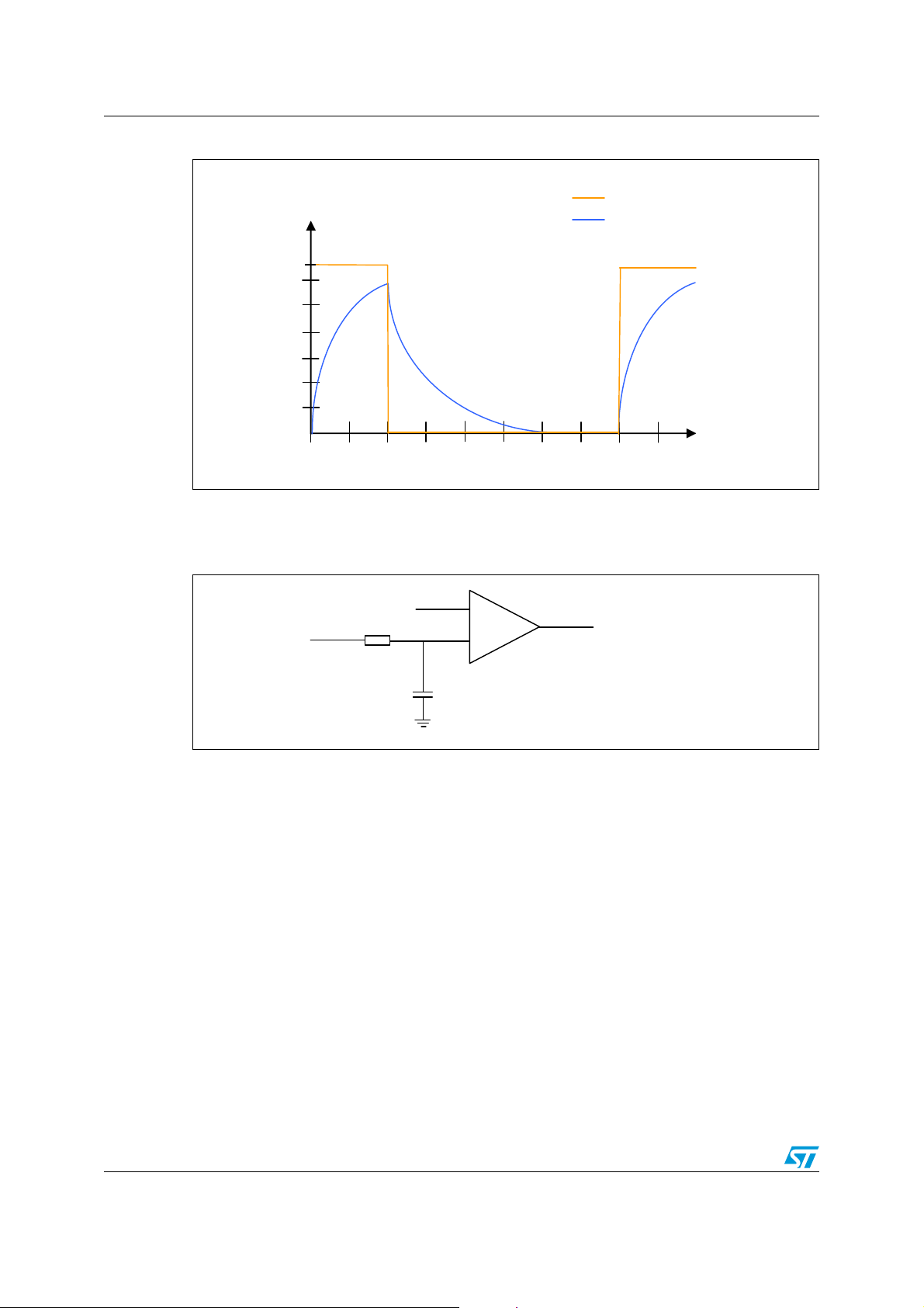
The reference signal is generated by charging a capacitor through a resistor. While the
voltage across the capacitor is being charged, it follows an exponential curve.
This exponential equation has been implemented in the software. The time taken by the
capacitor voltage to rise above the voltage value to be converted is used in the charge
equation to retrieve the digital conversion value.
Charge equation:
Where:
● Vmeas is the value to be mesaured
● V
● t is the time measured by timer2 when the comparator detects that the input voltage is
is the input voltage
DD
above the reference voltage
● T is the RC constant (here R=10 kΩ and C=100 nF so T= 1 ms)
The capacitor is charged and discharged using the timer 2 PWM on channel1/ PB0.
A timer is programmed to generate a 2 ms PWM with a duty cycle of 0.25. This 2-ms period
permits an ADC implementation using the full voltage range that the comparator tolerates.
The capacitor charging curve is shown in the following figure.
Doc ID 15651 Rev 1 3/12
Page 4
Application description AN2979
PWM output
Capacitor charging curve
V
DD
T(ms)
3.3
2.5
2
1.5
1
0.5
123456789
(V)
3
AI
-
+
C=100 nF
PB0/PC4
PA6
PD2
COMP_OUT
R=10 k7
Figure 1. Capacitor charging curve
The figure below shows the connection of the comparator to the required external
components.
Figure 2. Comparator connections
1. Condition: VDD=3.3 V, R=10 kΩ, C=100 nF
Note: When using the STM8L101-EVAL evaluation board you need to connect the PB0 pin to the
PC4 pin. This way you use the resistor and capacitor already present on the board (no
hardware needed). Pin PC4 is configured as input floating to avoid any conflict.
4/12 Doc ID 15651 Rev 1
Page 5

AN2979 Software description
param.h
param.c
ai15372
main.c
stm8l10x.h
stm8l10x.hstm8l10x.h
stm8l10x.h
stm8l10x tim stm8l10x comp
stm8l10x tim stm8l10x.comp
stm8l10x cl stm8l10x api
stm8l10x cl stm8l10x api
Application layer
API layer
Standard
peripheral drivers
STM8L101x
microcontroller
2 Software description
The software provided with this application note describes a way of implementing an A/D
converter (using a timer and analog comparator interrupts).
The application uses four peripherals:
● CLK: the clock enables and provides the correct clock frequency for the peripherals.
● COMP: the comparator detects when the input voltage is above the reference voltage
● TIM2: Timer 2 provides the 2 ms PWM with a duty cycle of 0.25 generating the
capacitor charge and discharge. Timer 2 Capture/compare interrupt routine handles
the conversion.
● GPIO: the general purpose I/O handles the I/O used.
● SPI: used to communicate with the LCD.
A generic file param.h contains the parameter values that can be modified in order to re-use
the application and adapt it easily to other conditions.
At the start, the LCD displays “STM8L ADC using COMP”. Then it continously displays the
measured values.
Figure 3. Application architecture & description
Note: The software can be compiled with Cosmic and Raisonance compilers. It contains projects
for STVD and Raisonance IDE.
A calibration of some parameters can be optionally set if “#define Calibration” is
uncommented in the param.h file.
Doc ID 15651 Rev 1 5/12
Page 6

Software description AN2979
ai15766
Configure the system clock to provide a master
clock frequency f
MASTER
= 16 MHz
Enable TIM2 peripheral clock
Configure PC4 as input floating
Configure PB0 as output push pull for the PWM
Comparator configuration
Enable comparator interface
Configure COMP2 channel3
With external reference and polarity high
Connect Comp2 output to the TIM2 input capture1
TIM configuration
TIM2 to generate the PWM
Enable TIM2 capture / compare interrupt enable
Enable general interrupts
SPI config
uration
Display on LCD
Configure COMP2 channel4
Compare to the reference value
Enable TIM2
Display on LCD
Start
Clock configuration
GPIO configuration
A/D converter
initialization
LCD configuration
Calibration
Optional
Start A/D conversion
End
ai15767
Get timer value
Get the conversion value
Clear TIM2 pending bit
Display on the LCD
Start
End
V
IN
>
V
REF
2.1 Application flowcharts
Figure 4. Main loop flowchart
Figure 5. Get conversion value flowchart
6/12 Doc ID 15651 Rev 1
Page 7

AN2979 Hardware description
AI
(COMP2_CH3)
PA 6
(COMP_REF)
R=10 kΩ
C=100 nF
STM8L10x
PB0
PC4
VSS
PD2
VDD
!$#INPUT
3 Hardware description
Figure 6. Circuit diagram
STM8L101 evaluation board settings:
■ Remove jumper JP2 to connect an external input voltage instead of the potentiometer
input. With the potentiometer RV1, the value is limited to 0.8 V and the signal is noisy (due
to the LCD). So the display on the LCD screen would not be stable.
■ Connect the external ADC voltage input directly to PD2.
■ Ground together the evaluation board and the external ADC signal.
■ An accurate 3.3 V MCU voltage can be tuned on the evaluation board using RV4.
Doc ID 15651 Rev 1 7/12
Page 8

Measurements and calibration AN2979
TRC× 10 10
3
×()100 10
9–
×()× 1 ms== =
T
ACC1
R
ACC1CACC1
× 9.8 10
3
×()90 10
9–
×()× 882 μs== =
T
ACC2
R
ACC2CACC2
× 10.2 10
3
×()110 10
9–
×()× 1.122 ms== =
V
meas
V
DD
1
t
T
---–
⎝⎠
⎛⎞
exp–
⎝⎠
⎛⎞
×=
V
measacc1
V
DD
1
t
T
acc1
-----------------–
⎝⎠
⎜⎟
⎛⎞
exp–
⎝⎠
⎜⎟
⎛⎞
×=
V
measacc2
V
DD
1
t
T
acc2
-----------------–
⎝⎠
⎜⎟
⎛⎞
exp–
⎝⎠
⎜⎟
⎛⎞
×=
4 Measurements and calibration
4.1 Typical measurements
The following values are given for information only.
Table 1. Measured value after conversion and margin error for V
Value to be measured (V) Measured value after conversion (V) Error (%)
0.25 0.204 18.4%
0.5 0.419 16.2%
0.8 0.704 12%
1 0.903 9.7%
1.25 1.14 8.8%
1.5 1.39 7.33%
1.75 1.628 6.97%
4.2 Precision of the measured value
When using the RC charge equation, the precision of the measured value depends on the
accuracy of the capacitor C and the resistor R.
Accuracy example:
if C=100 nF with 10% accuracy: C
if R=10 kΩ with 2% accuracy: R
=90 nF or C
acc1
=9.8 kΩ or R
acc1
acc2
acc2
=110 nF
=10.2 kΩ
DD
=3.3 V
Calculation of the RC constant:
Charge equations:
8/12 Doc ID 15651 Rev 1
Page 9

AN2979 Measurements and calibration
y = 3.3(1-exp(-x/0.882))
y = 3.3(1-exp(-x))
y = 3.3(1-exp(-x/1.122))
0.5
1
1.5
2
2.5
3
0.5
1
1.5 2
2.5
V
ms
Vmeas_max = 2.05
tmaxtacc1max tacc2max
tacc2max = 1.09 ms
tacc1max = 0.856ms
tmax = 0.970ms
The following figure shows the impact of the capacitor and resistor accuracy.
Figure 7. Charge equation depending on RC accuracy
Note: The results are not only impacted by the marging error due to hardware components but
4.3 How to get a better accuracy
4.3.1 Hardware solution
4.3.2 Software solution
1. In blue: V
measacc1
---- In red: V
---- In green: V
meas
measacc2
2. Condition: VDD=3.3 V
also by the accuracy of the MCU clock. In this example, the device works at a HSI frequency
of 16 MHz at 25 °C, that is, with a clock accuracy of 1% (refer to the datasheet).
The temperature variation also impacts the accuracy of the measured value as the
microcontroller, resistors and capacitors are temperature dependent.
The first solution is to choose components with a high accuracy value (this may imply a
higher cost).
The second solution is to calibrate the RC constant in the software using VDD as a
reference.
Implementation description
In order to perform the calibration, you need to uncomment the “#define calibration” in the
“param.h” file.
Doc ID 15651 Rev 1 9/12
Page 10

Measurements and calibration AN2979
AI
K7
K7
2K7
# N &
#ALIBRATIONINPUT
!$#INPUT
0$#/-0?#(
0$#/-0?#(
34- ,X 6
$$
0#
0"
0!
#/-0?2 %&
633
The calibration is then performed by firware and the RC constant is updated. This constant
is used in the charge equation.
On the STM8L101-EVAL evaluation board, the COMP2 channel 4 (PD3) is connected to
V
via a resistor bridge.
DD
Figure 8. Evaluation board calibration schematic
As V
=3.3 V, PD3 is a fixed value equal to 0.4 V
DD
In the file “param.h” you need to define the “expected_value” equal to 0.4 ( this value needs
to be updated if a different resistor bridge is used).
The specific function “Calibration()” configures the COMP2 Channel 4 and compares the
value measured on this channel with the expected value. This function then updates the RC
constant that will be used afterwards.
When the calibration is performed, the COMP2 configuration changes to use the Channel 3
(PD2).
The following table lists a few measurement examples with a calibration performed at
V
=3.3 V, R=10 kΩ and C=100 nF.
DD
Table 2. Accuracy measurement when the calibration is performed
Value to be measured (V) Measured value after conversion (V) Error (%)
0.25 0.233 6.8%
0.5 0.475 5%
0.8 0.792 1.25%
10.991%
1.2 1.211 0.92%
1.5 1.512 0.8%
1.75 1.784 1.9%
10/12 Doc ID 15651 Rev 1
Page 11

AN2979 Revision history
5 Revision history
Table 3. Document revision history
Date Revision Changes
12-Feb-2010 1 Intitial release.
Doc ID 15651 Rev 1 11/12
Page 12

AN2979
Please Read Carefully:
Information in this document is provided solely in connection with ST products. STMicroelectronics NV and its subsidiaries (“ST”) reserve the
right to make changes, corrections, modifications or improvements, to this document, and the products and services described herein at any
time, without notice.
All ST products are sold pursuant to ST’s terms and conditions of sale.
Purchasers are solely responsible for the choice, selection and use of the ST products and services described herein, and ST assumes no
liability whatsoever relating to the choice, selection or use of the ST products and services described herein.
No license, express or implied, by estoppel or otherwise, to any intellectual property rights is granted under this document. If any part of this
document refers to any third party products or services it shall not be deemed a license grant by ST for the use of such third party products
or services, or any intellectual property contained therein or considered as a warranty covering the use in any manner whatsoever of such
third party products or services or any intellectual property contained therein.
UNLESS OTHERWISE SET FORTH IN ST’S TERMS AND CONDITIONS OF SALE ST DISCLAIMS ANY EXPRESS OR IMPLIED
WARRANTY WITH RESPECT TO THE USE AND/OR SALE OF ST PRODUCTS INCLUDING WITHOUT LIMITATION IMPLIED
WARRANTIES OF MERCHANTABILITY, FITNESS FOR A PARTICULAR PURPOSE (AND THEIR EQUIVALENTS UNDER THE LAWS
OF ANY JURISDICTION), OR INFRINGEMENT OF ANY PATENT, COPYRIGHT OR OTHER INTELLECTUAL PROPERTY RIGHT.
UNLESS EXPRESSLY APPROVED IN WRITING BY AN AUTHORIZED ST REPRESENTATIVE, ST PRODUCTS ARE NOT
RECOMMENDED, AUTHORIZED OR WARRANTED FOR USE IN MILITARY, AIR CRAFT, SPACE, LIFE SAVING, OR LIFE SUSTAINING
APPLICATIONS, NOR IN PRODUCTS OR SYSTEMS WHERE FAILURE OR MALFUNCTION MAY RESULT IN PERSONAL INJURY,
DEATH, OR SEVERE PROPERTY OR ENVIRONMENTAL DAMAGE. ST PRODUCTS WHICH ARE NOT SPECIFIED AS "AUTOMOTIVE
GRADE" MAY ONLY BE USED IN AUTOMOTIVE APPLICATIONS AT USER’S OWN RISK.
Resale of ST products with provisions different from the statements and/or technical features set forth in this document shall immediately void
any warranty granted by ST for the ST product or service described herein and shall not create or extend in any manner whatsoever, any
liability of ST.
ST and the ST logo are trademarks or registered trademarks of ST in various countries.
Information in this document supersedes and replaces all information previously supplied.
The ST logo is a registered trademark of STMicroelectronics. All other names are the property of their respective owners.
© 2010 STMicroelectronics - All rights reserved
STMicroelectronics group of companies
Australia - Belgium - Brazil - Canada - China - Czech Republic - Finland - France - Germany - Hong Kong - India - Israel - Italy - Japan -
Malaysia - Malta - Morocco - Philippines - Singapore - Spain - Sweden - Switzerland - United Kingdom - United States of America
www.st.com
12/12 Doc ID 15651 Rev 1
 Loading...