

Page 1

AN2692
Application note
How to program/reprogram the ST10F269Zx Flash memory
Introduction
This application note provides software guidelines and examples to program the
ST10F269Zx. More generally, this application note is applicable to any ST10 variant with an
0.35 µm technology embedded Flash memory.
The first section gives an overview of the ST10F269Zx embedded Flash memory’s key
features. It also shows the differences between the ST10F269Zx and ST10F168.
The second section describes how to develop software for the ST10F269Zx embedded
Flash memory through guidelines, examples and tips.
The last section is dedicated to embedded application aspects. More specifically, it gives
advices for Flash memory field reprogramming.
This application note does not replace the ST10F269Zx product datasheet. It refers to it and
it is necessary to have a copy of it to follow some of the explanations.
March 2008 Rev 1 1/29
www.st.com
Page 2

Contents AN2692
Contents
1 Introduction to ST10F269Zx 0.35 µm embedded Flash memory . . . . . 6
1.1 Differences with ST10F168 . . . . . . . . . . . . . . . . . . . . . . . . . . . . . . . . . . . . 6
1.1.1 Single supply . . . . . . . . . . . . . . . . . . . . . . . . . . . . . . . . . . . . . . . . . . . . . . 6
1.1.2 New Erase/Program Controller . . . . . . . . . . . . . . . . . . . . . . . . . . . . . . . . 6
1.1.3 Improved granularity of block sizes . . . . . . . . . . . . . . . . . . . . . . . . . . . . . 6
1.2 Comparison with Standalone Flash memories . . . . . . . . . . . . . . . . . . . . . . 7
1.2.1 Similar but different erase/program commands . . . . . . . . . . . . . . . . . . . . 7
1.2.2 Description of the commands to the Flash memory Erase/Program
Controller . . . . . . . . . . . . . . . . . . . . . . . . . . . . . . . . . . . . . . . . . . . . . . . . . 7
1.2.3 Same Flash memory Status Register . . . . . . . . . . . . . . . . . . . . . . . . . . . 9
1.2.4 Boot block architecture . . . . . . . . . . . . . . . . . . . . . . . . . . . . . . . . . . . . . 10
1.2.5 Protection . . . . . . . . . . . . . . . . . . . . . . . . . . . . . . . . . . . . . . . . . . . . . . . . 10
1.2.6 Operating modes . . . . . . . . . . . . . . . . . . . . . . . . . . . . . . . . . . . . . . . . . . 11
2 Writing code for the ST10F269Zx with 0.35 µm embedded Flash . . . 12
2.1 ST10 programming constraints . . . . . . . . . . . . . . . . . . . . . . . . . . . . . . . . 12
2.1.1 Programming language . . . . . . . . . . . . . . . . . . . . . . . . . . . . . . . . . . . . . 12
2.2 Polling the Flash memory Erase/Program Controller . . . . . . . . . . . . . . . . 12
2.2.1 Ready/Busy signal . . . . . . . . . . . . . . . . . . . . . . . . . . . . . . . . . . . . . . . . . 12
2.2.2 Flash memory Status Register . . . . . . . . . . . . . . . . . . . . . . . . . . . . . . . 13
2.3 Flash memory mapping in the ST10F269Zx memory space . . . . . . . . . . 14
2.4 Program command . . . . . . . . . . . . . . . . . . . . . . . . . . . . . . . . . . . . . . . . . . 14
2.5 Erase commands . . . . . . . . . . . . . . . . . . . . . . . . . . . . . . . . . . . . . . . . . . . 16
2.6 Flash protection commands . . . . . . . . . . . . . . . . . . . . . . . . . . . . . . . . . . . 17
2.6.1 Set Block Protection . . . . . . . . . . . . . . . . . . . . . . . . . . . . . . . . . . . . . . . 17
2.6.2 Set Code Protection . . . . . . . . . . . . . . . . . . . . . . . . . . . . . . . . . . . . . . . . 17
2.7 Other Flash memory commands . . . . . . . . . . . . . . . . . . . . . . . . . . . . . . . 19
2.8 Tips to reduce Flash memory programming and erase times . . . . . . . . . 19
2.8.1 Reducing the programming time . . . . . . . . . . . . . . . . . . . . . . . . . . . . . . 19
2.8.2 Reducing erase times . . . . . . . . . . . . . . . . . . . . . . . . . . . . . . . . . . . . . . 19
3 Embedded application aspects . . . . . . . . . . . . . . . . . . . . . . . . . . . . . . . 21
3.1 Reading the Flash memory while erasing or programming . . . . . . . . . . . 21
2/29
Page 3

AN2692 Contents
3.1.1 Minimum software to be copied into the on-chip RAM . . . . . . . . . . . . . . 21
3.1.2 Maximizing programming performance at system level . . . . . . . . . . . . . 21
3.1.3 Erase Suspend and Resume commands . . . . . . . . . . . . . . . . . . . . . . . 22
3.2 Field reprogramming with ST10F269Zx . . . . . . . . . . . . . . . . . . . . . . . . . . 22
3.2.1 Field events and Flash memory reliability . . . . . . . . . . . . . . . . . . . . . . . 22
3.2.2 Reset . . . . . . . . . . . . . . . . . . . . . . . . . . . . . . . . . . . . . . . . . . . . . . . . . . . 22
3.2.3 List of events and suggested handling methods . . . . . . . . . . . . . . . . . . 23
3.2.4 Generic aspects of Flash field reprogramming . . . . . . . . . . . . . . . . . . . 24
3.3 Ruggedized aspects . . . . . . . . . . . . . . . . . . . . . . . . . . . . . . . . . . . . . . . . . 25
3.3.1 Checksum . . . . . . . . . . . . . . . . . . . . . . . . . . . . . . . . . . . . . . . . . . . . . . . 25
3.3.2 Initialization of unused memory locations . . . . . . . . . . . . . . . . . . . . . . . 25
4 Quick summary . . . . . . . . . . . . . . . . . . . . . . . . . . . . . . . . . . . . . . . . . . . . 26
5 Conclusion . . . . . . . . . . . . . . . . . . . . . . . . . . . . . . . . . . . . . . . . . . . . . . . . 27
6 Revision history . . . . . . . . . . . . . . . . . . . . . . . . . . . . . . . . . . . . . . . . . . . 28
3/29
Page 4

List of tables AN2692
List of tables
Table 1. Commands for ST10 with 0.35 µm embedded Flash memory . . . . . . . . . . . . . . . . . . . . . . . 7
Table 2. Flash memory block mapping (lower 32 Kbytes of memory) . . . . . . . . . . . . . . . . . . . . . . . 14
Table 3. Document revision history . . . . . . . . . . . . . . . . . . . . . . . . . . . . . . . . . . . . . . . . . . . . . . . . . 28
4/29
Page 5

AN2692 List of figures
List of figures
Figure 1. Data polling flow . . . . . . . . . . . . . . . . . . . . . . . . . . . . . . . . . . . . . . . . . . . . . . . . . . . . . . . . . 13
Figure 2. Verification algorithm for word programming . . . . . . . . . . . . . . . . . . . . . . . . . . . . . . . . . . . 14
Figure 3. Verification algorithm for erasing . . . . . . . . . . . . . . . . . . . . . . . . . . . . . . . . . . . . . . . . . . . . 16
5/29
Page 6

Introduction to ST10F269Zx 0.35 µm embedded Flash memory AN2692
1 Introduction to ST10F269Zx 0.35 µm embedded Flash
memory
This section describes the improvements made from the ST10F168 and the differences with
standalone Flash memories.
1.1 Differences with ST10F168
1.1.1 Single supply
ST10 variants with 0.35 µm embedded Flash memories do not require specific a supply for
programming. On-chip charge pumps provide the necessary supply from the external single
5 V supply.
1.1.2 New Erase/Program Controller
The 0.35 µm Erase/Program Controller was changed to be more similar to the one of
standalone Flash memories: erasing and programming of Flash memory cells is no more
done by the ST10. This allows:
● Savings on system stack: Space no longer needs allocated on the ST10 system
stack for erasing and programming,
● Improved efficiency during programming: ST10 CPU can be used to handle
communication during the time where the Erase/Program Controller is dealing with the
Flash memory
● Improved clock scheme: the Flash Erase/Program Controller has its own clock; there
is no more need to specify it to the CPU clock. This also simplifies the handling of
special events (like PLL unlock) during erasing/programming.
1.1.3 Improved granularity of block sizes
The ST10F269Zx 0.35 µm embedded Flash memory has an improved block granularity
(smaller blocks) and also features a boot block organization:
● Block size is 64 Kbytes for standard blocks,
● Small blocks for the 4 boot blocks (16 Kbyte, then 8 Kbyte, 8 Kbyte, 32 Kbyte).
6/29
Page 7
AN2692 Introduction to ST10F269Zx 0.35 µm embedded Flash memory
1.2 Comparison with Standalone Flash memories
1.2.1 Similar but different erase/program commands
The Erase/Program Controller of ST10F269Zx is derived from the Common Flash memory
Interface:
● To keep the same level of proven safety, the special sequence of commands of
standalone Flash memories has been kept,
● To differentiate embedded Flash memories from external Flash memories, the value of
the commands (addresses and data) have been slightly modified.
1.2.2 Description of the commands to the Flash memory Erase/Program Controller
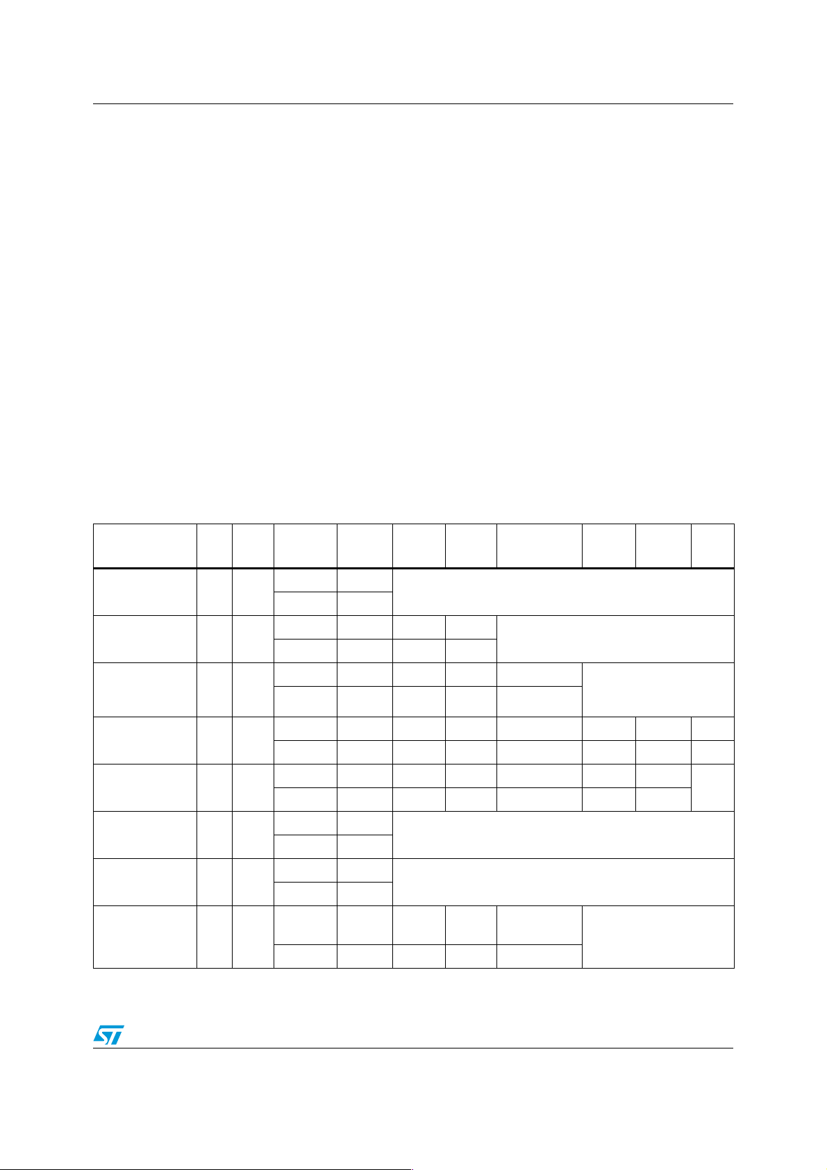
Ta bl e 1 describes the commands allowed with the ST10F269Zx Erase/Program Controller.
Commands to the Flash memory are defined by a sequence of ST10F269Zx write cycles
with specific addresses and data within the Flash memory address range. The length of the
sequence varies from 1 cycle (e.g.: Read/Reset) to 6 cycles (Chip Erase).
The Block Erase command can be extended by 1 cycle per additional block to erase. This
translates in a maximum of 12 cycles for the ST10F269Zx.
Table 1. Commands for ST10 with 0.35 µm embedded Flash memory
Instruction Mne Cycle
Read/Reset RD 1+
Address/
Data
(2)
Addr.
st
1
cycle
X
2nd
cycle
3rd
cycle
th
4
Read Memory Array until a new write cycle is initiated
Data xxF0h
(2)
Read/Reset RD 3+
Addr.
Data xxA8h xx54h xxF0h
Addr.
x1554h x2AA8h xxxxxh
Read Memory Array until a new write
cycle is initiated
(2)
x1554h x2AA8h x1554h WA Read Data Polling or
Program Word PW 4
Data xxA8h xx54h xxA0h WD
(2)
Addr.
x1554h x2AA8h x1554h x1554h x2AA8h BA BA’
Block Erase BE 6
Data xxA8h xx54h xx80h xxA8h xx54h xx30h xx30h
(2)
Addr.
x1554h x2AA8h x1554h x1554h x2AA8h x1554h
Chip Erase CE 6
Data xxA8h xx54h xx80h xxA8h xx54h xx10h
(2)
Erase Suspend ES 1
Erase Resume ER 1
Addr.
Data xxB0h
(2)
Addr.
Data xx30h
X
Read until Toggle stops, then read or program all data
needed from block(s) not being erased then Resume Erase.
X
Read Data Polling or Toggle bit until Erase completes or
Erase is suspended another time.
cycle
(1)
th
5
6th
cycle
cycle
Toggle bit until program
completes.
7th
cycle
(3)
Note
(4)
Set Block/Code
Protection
SP 4
Addr.
(2)
x2A54h x15A8h x2A54h
Any odd word
address
Data xxA8h xx54h xxC0h WPR
7/29
(5)
(6)
Page 8
Introduction to ST10F269Zx 0.35 µm embedded Flash memory AN2692
cycle
(1)
(continued)
th
5
6th
cycle
Read Protection Register
(5)
until a new write cycle is
cycle
initiated.
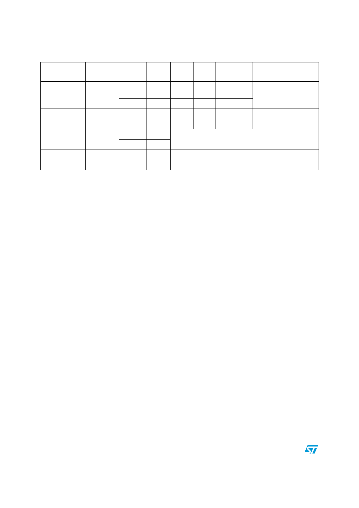
Table 1. Commands for ST10 with 0.35 µm embedded Flash memory
Instruction Mne Cycle
Read Protection
Status
RP 4
Address/
Data
(2)
Addr.
Data xxA8h xx54h xx90h Read PR
(2)
Block Temporary
Unprotection
Code Temporary
Unprotection
Code Temporary
Protection
1. Mne = mnemonic, X = Don’t Care.
WA = Write Address: address of memory location to be programmed.
WD = Write Data: 16-bit data to be programmed.
BA = Block address.
2. Address bit A14, A15 and above are don’t care for coded address inputs.
3. Optional, additional blocks addresses must be entered within a timeout delay (96 µs) after last write entry, timeout status
can be verified through FSB.3 value. When full command is entered, read Data Polling or Toggle bit until Erase is
completed or suspended.
4. Read data polling or toggle bit until erase completes.
5. Odd word address = 4n-2 where n = 0, 1, 2, 3..., e.g. 0002h, 0006h, etc.
6. WPR = Write protection register. To protect code, bit 15 of WPR must be ‘0’. To protect block N (N=0,1,...), bit N of WPR
must be ‘0’. Bit that are already at ‘0’ in protection register must also be ‘0’ in WPR, else a writing error will occurs (it is not
possible to write a ‘1’ in a bit already programmed at ‘0’).
7. MEM = any address inside the Flash memory space. Absolute addressing mode must be used (MOV MEM, Rn), and
instruction must be executed from Flash memory space.
BTU 4
CTU 1
CTP 1
Addr.
Data xxA8h xx54h xxC1h xxF0h
(2)
Addr.
Data FFFFh
(2)
Addr.
Data FFFBh
st
1
cycle
x2A54h x15A8h x2A54h
2nd
cycle
3rd
cycle
th
4
Any odd word
address
x2A54h x15A8h x2A54h X
(7)
MEM
Write cycles must be executed from Flash.
(7)
MEM
Write cycles must be executed from Flash.
7th
cycle
Flash commands and ST10 pipeline effect
Due to the ST10F269Zx pipeline effect, all erase and program commands must not be
immediately followed by a JMPx, CALLx or RETx instruction.
For any erase or program command, a NOP instruction must be inserted after sending the
last command to the Flash memory Erase/Program Controller.
When not implemented, and when the ST10F269Zx is in bootstrap mode with the code
running from the XRAM or an external memory, the TestFlash may be selected instead of
the user Flash memory (for details, please refer to ST10F269Zx errata sheet).
8/29
Page 9

AN2692 Introduction to ST10F269Zx 0.35 µm embedded Flash memory
1.2.3 Same Flash memory Status Register
The Flash memory Status Register is used to flag the status of the Flash memory and the
result of an operation.
To maximize the reuse of Flash memory programming software, the Flash memory Status
Register of standalone Flash memories has been kept.
This register can be accessed by read cycles during Program/Erase Controller (P/E.C.)
operations. Erase/program operations can be controlled by data polling on the FSB7 bit of
the Status Register. Toggle detection is indicated on FSB6 and FSB2, error on FSB5 and
erase timeout on the FSB3 bit. Any read attempt from the Flash memory during an erase or
a program operation will automatically output these five bits. The P/E.C. sets bits FSB2,
FSB3, FSB5, FSB6 and FSB7. Other bits are reserved for future use and should be
masked.
Flash memory Status
Note: The address of the Flash memory Status Register is the address of the word being
programmed when a programming operation is in progress, or an address within the block
being erased when an erasing operation is in progress.
15 14 13 12 11 10 9 8 7 6 5 4 3 2 1 0
--------FSB.7FSB.6FSB.5-FSB.3FSB.2--
FSB.7 bit Flash Status Bit 7: Data Polling bit
FSB.6 bit Flash Status Bit 6: Toggle bit
FSB.5 bit Flash Status Bit 5: Error bit
FSB.3 bit Flash Status Bit 3: Erase Timeout bit
RRR RR
Programming operation: this bit outputs the complement of the bit 7 of the word being programmed,
and after completion, will output the bit 7 of the programmed word.
Erasing operation: outputs a ‘0’ during erasing, and ‘1’ after erasing completion.
If the block(s) selected for erasure is (are) protected, FSB.7 is set to ‘0’ for about 100 µs, and then
returns to the previous addressed memory data value.
FSB.7 also flags the Erase Suspend mode by switching from ‘0’ to ‘1’ at the start of Erase Suspend.
During program operation in Erase Suspend mode, FSB.7 has the same behavior as in normal
program execution outside the Erase Suspend mode.
Programming or erasing operations: successive read operations of Flash Status register deliver
complementary values. FSB.6 toggles each time the Flash Status Register is read. The program
operation is completed when two successive reads yield the same value. The next read will output
the last programmed bit, or a ‘1’ after an erase operation
FSB.6 is set to‘1’ if a read operation is attempted on an Erase Suspended block. In addition, an
Erase Suspend/Resume command will cause FSB.6 to toggle.
This bit is set to ‘1’ when there is a failure of a program, Block or Chip Erase operation.This bit is
also set if a user tries to program a bit to ‘1’ to a Flash memory location that is currently
programmed with ‘0’.
The error bit is reset after a Read/Reset command.
In case of success, the Error bit is set to ‘0’ during Program or Erase and then outputs the last
programmed bit or a ‘1’ after erasing
This bit is set to ‘1’ by the P/E.C. when the last Block Erase command has been entered to the
Command Interface and is awaiting the erase start. When the timeout period is finished, after
96 µs, FSB.3 returns to ‘1’.
9/29
Page 10

Introduction to ST10F269Zx 0.35 µm embedded Flash memory AN2692
FSB.2 bit Flash Status Bit 2: Toggle bit
This toggle bit, together with FSB.6, can be used to determine the chip status during the Erase or
Erase Suspend mode. It can also be used to identify the block being Erase-Suspended. A Read
operation will cause FSB.2 to Toggle during the Erase mode. If the Flash memory is in Erase
Suspend mode, a read operation from the Erase-Suspended block or a program operation into the
Erase-Suspended block will cause FSB.2 to toggle.
When the Flash memory is in program mode during Erase Suspend, FSB.2 will be read as ‘1’ if
address used is the address of the word being programmed.
After Erase completion with an error status, FSB.2 will toggle when reading the faulty sector.
1.2.4 Boot block architecture
The ST10F269Zx with a 0.35 µm embedded Flash memory has the same boot blocks as
the M29F400 standalone Flash memory: 4 boot blocks (16 Kbyte, then 8 Kbyte, 8 Kbyte and
32 Kbyte).
1.2.5 Protection
Compared to standalone Flash memories, the ST10F269Zx with an embedded Flash
memory provides 2 different protections:
● Block protection, as already implemented on ST standalone Flash memories, protects
each block against inadvertent erasing,
● Code protection, is a set of new commands to protect the proprietary code written in
the Flash memory: code protection disables data operand accesses and program
branches from any location outside the embedded Flash memory.
The different protections are controlled through the Flash memory Protection Register. It is
identical to the one of standalone Flash memories except for the code protection.
The Flash memory Protection Register is a non-volatile register that contains the protection
status. This register can be read by using the Read Protection Status (RP) command, and
programmed by using the dedicated Set Block/Code Protection commands.
Flash memory Protection Register (PR)
1514131211109876543210
CP BP6 BP5 BP4 BP3.3 BP2.2 BP1 BP0
BPx bits Block x Protection bit (x = 0...10)
‘0’: block protection is enabled for block x. Programming or erasing the block is not possible, unless
a Block Temporary Unprotection command is issued.
1’: block protection is disabled for block x.
Bit is ‘1’ by default, and can be permanently programmed to ‘0’ using the Set Block Protection
command but then cannot be set to ‘1’ again. It is therefore possible to temporarily disable the block
protection using the Block Temporary Unprotection command.
10/29
Page 11

AN2692 Introduction to ST10F269Zx 0.35 µm embedded Flash memory
CP bit Code Protection bit
‘0’: Flash code protection is enabled. Read accesses to the Flash memory or execution not
performed in the Flash memory itself are not allowed, the returned value will be 009Bh, whatever
the contents of the Flash memory.
1’: Flash code protection is disabled: read accesses to the Flash memory from external or internal
RAM are allowed
Bit is ‘1’ by default, and can be programmed permanently to ‘0’ using the Set Code Protection
command but then cannot be set to ‘1’ again. It is therefore possible to temporally disable the code
protection using the Code Temporary Unprotection command.
1.2.6 Operating modes
Unlike the standalone Flash memory, the ST10F269Zx embedded Flash memory has three
different operating modes:
● User mode
● Bootstrap mode
● Te s t m o d e
These modes are selected upon reset by pulling down some specific lines of Port0. Since
these modes do not exist in the standalone Flash memory, it is recommended to verify that
the embedded Flash memory is in the right mode before erasing or programming it.
The EMUCON register shows which operating mode is active.
EMUCON(FE0Ah/ 05h)
15 14 13 12 11 10 9 8 7 6 5 4 3 2 1 0
--------TMOD1TMOD2TMOD3xxxxx
RRR
TMOD1 bit
(EMUCON.7
TMOD2 bit
(EMUCON.6
TMOD3 bit
(EMUCON.5
Note: Only 1 of these bits can be active at a time. The three bits are read-only.
TESTMODE1 Control bit
’0’: TESTMODE1 is not active
)
’1’: TESTMODE1 is active
This bit is set if P0L.2 = 0 during hardware reset.
TESTMODE2 Control bit
’0’: Bootstrap Loader is not active
)
’1’: Bootstrap Loader is active
This bit is set if P0L.[5..3] = 101 during hardware reset.
TESTMODE3 Control bit
’0’: TESTMODE3 is not active
)
’1’: TESTMODE3 is active
This bit is set if P0L.2[5..3] = 100 or 011 during hardware reset.
Before performing any operation on the Flash memory, the user must verify that the
Flash memory is really in the desired operating mode:
● To program the Flash memory in the Bootstrap mode, check that the TMOD2 bit is set
● To program the Flash memory in the User mode, check that all TMODx bits are cleared.
11/29
Page 12

Writing code for the ST10F269Zx with 0.35 µm embedded Flash AN2692
2 Writing code for the ST10F269Zx with 0.35 µm
embedded Flash
2.1 ST10 programming constraints
2.1.1 Programming language
Direct addressing is not allowed for command sequences. All addresses of command cycles
shall be defined only with register-indirect addressing mode.
As the compiler may generate indirect addressing, the part of the software that generates
the commands to the Flash memory should be written in assembly. Still, the part of the
software that is not generating the commands can be in higher-level language (e.g.: C).
Indirect addressing
For command instructions, address bits A14, A15, A16 and A17 are don’t care, provided
that the generated address falls within the Flash memory space.
This is used to simplify the use of DPP registers when generating commands to the Flash
memory: any DPP already pointing to data in the Flash memory space can be used to write
commands to the Flash memory.
● Tip: It is also possible to use the extended segment or extended page instructions for
addressing the Flash memory.
2.2 Polling the Flash memory Erase/Program Controller
As soon as the Erase/Program Controller (E./P.C.) receives the last command of a
command sequence, it starts executing the command. During command execution, the
E./P.C. status is indicated by 2 sources:
● The Flash memory Status Register
● The Ready/Busy signal
The Flash memory automatically resumes the read mode after the completion of the
command.
2.2.1 Ready/Busy signal
The Ready/Busy (R/B) signal is connected to the XPER2 interrupt node (XP2IC). When R/B
is high, the Flash memory is busy with a program or erase operation and will not accept any
additional program or erase instruction. When R
read/write or erase operation. The R
Suspend mode.
This signal can be polled by reading the XP2IC register, or can be used to trigger an
interrupt when the Flash memory goes from Busy to Ready.
This feature may not be available for all ST10 variants in 0.35 µm Flash memory technology.
Please, check the product datasheet.
/B is also low when the memory is put in Erase
/B is low, the Flash is ready for any
12/29
Page 13

AN2692 Writing code for the ST10F269Zx with 0.35 µm embedded Flash
2.2.2 Flash memory Status Register
The Flash memory Status Register is described in Section 1.2.3: Same Flash memory
Status Register.
This method of polling the ST10F269Zx embedded Flash memory is recommended and
used in the code examples in this document. There is another method to verify the
completion of a Flash memory operation, it is called the “data polling flow”. It uses the
Toggle bit of the Flash Status Register. The algorithm is described in the figure below.
Figure 1. Data polling flow
Start
Read FSB.2, FSB.5, FSB.6 bits
No
No
Pass
ai14876
No
FSB.2, FSB.6
toggle?
Yes
FSB.5 = 1?
Yes
Read FSB.2, FSB.5, FSB.6 bits
FSB.2, FSB.6
toggle?
Yes
Fail
The two read accesses to the Flash memory Status Register must be made consecutively.
The following sequence must be executed:
EXTS Ra, #1 ;use EXTended addressing for next MOV instruction
MOV Ry, [Rx] ;read Flash Status register (FSB) in Ry
EXTS Ra, #1 ;use EXTended addressing mode for next MOV instruction
MOV Rz, [Rx] ;read Flash Status register (FSB) in Rz
Then, the Rz and Ry registers are compared to check the toggling of
the bit.
13/29
Page 14

Writing code for the ST10F269Zx with 0.35 µm embedded Flash AN2692
2.3 Flash memory mapping in the ST10F269Zx memory space
As defined for all ST10 derivatives, the lower 32 Kbyte part of the embedded Flash memory
can be mapped to two different segments.
The Flash memory mapping is controlled by the ROMS1 bit in the SYSCON register.
Table 2. Flash memory block mapping (lower 32 Kbytes of memory)
(1)
Block
Addresses (Segment 0) Addresses (Segment 1) Size (Kbytes)
0
1
2
1. The memory mapping of the other block is independent of the ROMS1 bit.
00 0000h to 00 3FFFh
00 4000h to 00 5FFFh
00 6000h to 00 7FFFh
01 0000h to 01 3FFFh
01 4000h to 01 5FFFh
01 6000h to 01 7FFFh
16
8
8
2.4 Program command
In the examples hereafter, the 16-bit registers R11 and R12 are used as auxiliary registers
for indirect addressing.
The following examples use DPP0. All that is needed is to make sure that DPP0 points to
the active Flash memory area.
To be independent of the mapping of sector 0, DPP is set to point to segment 2 (that is:
DPP0 = 08h).
Note: The NOP instruction must be added after the last erase or program command to avoid the
ST10 pipeline effect (see Flash commands and ST10 pipeline effect on page 8).
Figure 2 shows the algorithm for word programming verification.
Figure 2. Verification algorithm for word programming
Program Word command
Yes
FSB.7, DATA.7
FSB.5 = 0?
FSB.7, DATA.7
14/29
Data polling
Yes
No
No
Yes
No
Programming OKProgramming error
ai14877
Page 15

AN2692 Writing code for the ST10F269Zx with 0.35 µm embedded Flash
Example: Performing a Program Word command
Let us assume that in the initialization phase the lowest 32 Kbytes of Flash memory (sector
0) have been mapped to segment 1. The data to be written is loaded into register R13, the
address to be programmed is loaded into registers R11/R12 (segment number into R11,
segment offset into R12).
; sending of the programming command to the Flash
MOV R5, #01554h ;load auxilary register R5 with command address
;(used in command cycle 1)
MOV R6, #02AA8h ;load auxilary register R6 with command address
SXCT DPPO, #08h ;push data page pointer 0 and load it to point
MOV R7, #0A8h ;load register R7 with 1st CI enable command
MOV [R5], R7 ;command cycle 1
MOV R13, #054h ;load register R7 with 2nd CI enable command
MOV [R6], R7 ;command cycle 2
MOV R13, #0A0h ;load register R7 with Program Word command
MOV [R5], R7 ;command cycle 3
POP DPP0 ;restore DPP0: following addressing to the Flash
EXTS R11, #1 ;use EXTended addressing for next MOV instruction
MOV [R12], R13 ;command cycle 4: the E/P.C. starts execution of
NOP ;pipeline effect: make sure there is no JMPx, no
;no JMPx, no RETx or no CALLx instruction here
; Data_Polling after word programming:
data_polling:
EXTS R11, #1 ;use EXTended addressing for next MOV instruction
MOV R7, [R12] ;read Flash Status register (FSB) in R7
MOV R6, R7 ;save it in R6 register
XOR R7, R13
JNB R7.7, Prog_OK
;(used in command cycle 2)
;to segment 2
;will use EXTended instructions
;R11 contains the segment to be programmed
;R12 contains the segment offset address to be programmed
;R13 contains the data to be programmed
;program command
;Check if FSB.7 = Data.7 (i.e. R7.7 = R13.7)
;Check if FSB.5 = 1 (Programming Error)
JNB R6.5, Data_Polling
EXTS R11, #1 ;use EXTended addressing for next MOV instruction
MOV R7, [R12] ;read Flash Status register (FSB) in R7
XOR R7, R13
JNB R7.7, Prog_OK
Prog_Error:
MOV R7, #0F0h ;load register R7 with Read/Reset command
EXTS R11, #1 ;use EXTended addressing for next MOV instruction
MOV R12], R7 ;address is don’t care for Read/Reset command
... ;here place specific Error handling code
...
...
Prog_OK:
....
....
;Programming Error: verify is Flash programmed data is OK
;Check if FSB.7 = Data.7
;Programming failed: Flash remains in Write Operation.
;To go back to normal Read operations, a Read/Reset
;command must be performed
;When programming operation finshed succesfully, Flash is set
;back automatically to normal Read Mode
15/29
Page 16

Writing code for the ST10F269Zx with 0.35 µm embedded Flash AN2692
2.5 Erase commands
Figure 3 shows the algorithm for erasing verification.
Figure 3. Verification algorithm for erasing
Erase command
Data polling
Yes
FSB.7 = 0
No
FSB.5 = 0?
No
FSB.7 = 1
No
Yes
Yes
Erase OKErase error
ai14878
Example: Performing the Block Erase command.
Let us assume that in the initialization phase the lowest 32 Kbytes of Flash memory (sector
0) have been mapped to segment 1. The R11/R12 registers contain an address related to
the block to be erased (segment number in R11, segment offset in R12, e.g.: R11 = 01h,
R12= 4000h will erase block 1 - first 8 Kbyte block).
; sending of the erasing command to the Flash
MOV R5, #01554h ;load auxilary register R5 with command address
MOV R6, #02AA8h ;load auxilary register R6 with command address
SXCT DPPO, #08h ;push data page pointer 0 and load it to point
MOV R7, #0A8h ;load register R7 with 1st CI enable command
MOV [R5], R7 ;command cycle 1
MOV R13, #054h ;load register R7 with 2nd CI enable command
MOV [R6], R7 ;command cycle 2
MOV R13, #080h ;load register R7 with Block Erase command
MOV [R5], R7 ;command cycle 3
MOV R7, #0A8h ;load register R7 with 1st CI enable command
MOV [R5], R7 ;command cycle 4
MOV R13, #054h ;load register R7 with 2nd CI enable command
MOV [R6], R7 ;command cycle 5
POP DPP0 ;restore DPP0: following addressing to the Flash
MOV R7, #030h ;load register R7 with erase confirm code
EXTS R11, #1 ;use EXTended addressing for next MOV instruction
MOV [R12], R7 ;command cycle 6: the E/P.C. starts execution of ;Erase
;(used in command cycle 1)
;(used in command cycle 2)
;to segment 2
;will use EXTended instructions
;R11 contains the segment of the block to be erased
;R12 contains the segment offset address of the block
Command after 96us timeout delay
16/29
Page 17

AN2692 Writing code for the ST10F269Zx with 0.35 µm embedded Flash
;additional block commands may be sent here before the ;96 µs
timeout expires.
; erase polling during block erase
Erase_Polling:
EXTS R11, #1 ;use EXTended addressing for next MOV instruction
MOV R7, [R12] ;read Flash Status register (FSB) in R7
JB R7.7, Erase_OK
;Check if FSB.7 = ‘1’ (i.e. R7.7 = ‘1’)
JNB R7.5, Erase_Polling
Erase_Error:
MOV R7, #0F0h ;load register R7 with Read/Reset command
EXTS R11, #1 ;use EXTended addressing for next MOV instruction
MOV [R12], R7 ;address is don’t care for Read/Reset command
... ;here place specific Error handling code
...
...
Erase_OK:
....
....
;Check if FSB.5 = 1 (Erasing Error)
;Programming failed: Flash remains in Write Operation.
;To go back to normal Read operations, a Read/Reset ;command
must be performed
;When erasing operation finshed succesfully, Flash is ;set back
automatically to normal Read Mode
2.6 Flash protection commands
2.6.1 Set Block Protection
The Set Block Protection command is used to protect the internal Flash memory blocks
against inadvertent erasing and/or programming.
For security reasons, once set, the protection cannot be removed, even after erasing the
Flash memory. It can only be temporarily disabled using the Block Temporary Unprotection
command.
2.6.2 Set Code Protection
the Set Code Protection command is used to disable any read or jump to the ST10
embedded Flash memory from another memory (like internal RAM, external memory).
For security reasons, once set, the code protection is permanent and cannot be cleared,
even after erasing the Flash memory. Code protection can only be temporarily disabled
using the Code Temporary Unprotection command.
Code Temporary Unprotection remains active until a Code Temporary Protection command
is executed or until reset (reset via the Flash Command Interface, hardware, software,
watchdog).
Using code protection with ST10
When code protection is set, and when code may be executed from another memory before
resuming code execution from the on-chip-Flash memory, the code protection should be
disabled before calling the routine in the other memory. If not, a Trap #00 illegal instruction
will be generated when jumping back to the on-chip Flash memory.
17/29
Page 18

Writing code for the ST10F269Zx with 0.35 µm embedded Flash AN2692
Code protection and bootstrap loader
The code protection also applies in bootstrap mode: in ST10 bootstrap loader mode, it is not
possible to read the Flash memory or to jump to any address within the embedded Flash
memory.
Code protection and block 0 protection
When code protection is set, it is no longer possible to dump the Flash memory contents. In
addition, code protection also protects all blocks against erroneous erase or program.
When code protection is set, the Code Temporary Unprotection command should be
executed prior to any erase or program command. As explained before, this command
should be executed with the code running from the Flash memory.
Example: Performing the Read Protection Status command
;********************************************************************************
;Read_Block_Protection
;INPUT : NONE
;OUTPUT: R0 contain the status of each block (if bit x is set, block x is protected)
;********************************************************************************
Read_Block_Protection proc near
; R0 = segment of Flash
push R1 ; R1 = First addr to write
push R2 ; R2 = Second addr to write
push R3 ; R3 = Data
push R4 ; R3 = Data
push R5 ; R5 = pointer to data status
movR0, dpp2:Flash_Seg
mov R1, #Even_comm ; Retreive the even command addr
mov R2, #Odd_comm; Retreive the odd command addr
mov R3, #Val1
exts R0, #1
mov[R1],R3; First write
mov R3, #Val2
exts R0, #1
mov[R2],R3; second write
mov R3, #090h
exts R0, #1
mov[R1],R3; third write
MOV R2,#8; R2 contain the number of block that remain to read
MOV R3,#0; R3 will contain the status
MOV R4,#1; R4 Mask for status
MOV R1, R0
EXTS #MONITOR_SEG,#1
MOVR5, #flash_status
POP R5 ; R5 = pointer to data status
POP R4
POP R3
POP R2
POP R1
RET
Read_Block_Protection ENDP
Code protection and Read Protection Status command
The Read Protection Status command clears the effect of a previous Code Temporary
Unprotection command.
18/29
Page 19

AN2692 Writing code for the ST10F269Zx with 0.35 µm embedded Flash
2.7 Other Flash memory commands
Example: Performing the Read/Reset command
Let us assume that in the initialization phase the lowest 32 Kbytes of Flash memory (sector
0) have been mapped to segment 1.
According to the usual way of ST10 data addressing with data page pointers, address bits
A15 and A14 of a 16-bit command write address select the data page pointer (DPP) which
contains the upper 10 bits to build the 24-bit physical data address. Address bits A13...A0
represent the address offset. As the bits A14...A17 are don’t care when writing a Flash
memory command in the Command Interface (CI), we can choose the most convenient
DPPx register for address handling.
The following examples are making use of DPP0. All that is needed is to make sure that
DPP0 points to the active Flash memory space.
To be independent of the mapping of sector 0, all the DPPs used for Flash memory address
handling are set to point to segment 2.
For this reason DPP0 is loaded with value 08h (00 0000 1000b).
MOV R5, #01554h ;load auxilary register R5 with command address
MOV R6, #02AA8h ;load auxilary register R6 with command address
SCXT DPPO, #08h ;push data page pointer 0 and load it to point
MOV R7, #0A8h ;load register R7 with 1st CI enable command
MOV [R5], R7 ;command cycle 1
MOV R7, #054h ;load register R7 with 2cd CI enable command
MOV [R6], R7 ;command cycle 2
MOV R7, #0F0h ;load register R7 with Read/Reset command
MOV [R5], R7 ;command cycle 3. Address is don’t care
POP DPP0 ;restore DPP0 value
;(used in command cycle 1)
;(used in command cycle 2)
;to segment 2
2.8 Tips to reduce Flash memory programming and erase times
2.8.1 Reducing the programming time
When block protection is enabled, Block Temporary Unprotection commands shall be sent
before any erase or program command.
As block unprotection remains active till the next reset, this means it is not necessary to
repeat the command for each word to program.
2.8.2 Reducing erase times
Reducing the erase time is simple with ST10F269Zx 0.35 µm embedded Flash memory.
Several charge pumps are provided for each block, so erasing two blocks does not take
twice as long as erasing one block (erasing 2 blocks still takes longer than erasing one block
however). To benefit from the parallel erase, it is important to issue all the blocks you want
with one Block Erase command. The Chip Erase command also erases the blocks in
parallel.
19/29
Page 20

Writing code for the ST10F269Zx with 0.35 µm embedded Flash AN2692
Erasing a block of data
Erase commands perform two operations: first, they individually program each word to
0000h, then they use the tunnelling to set all bits to "1" at the same time. The time taken to
erase a block can be reduced by more than 50% if all word are already programmed to
0000h.
This specificity can be used in applications where blocks of data are copied from 1 block to
another and the old block is marked as "dirty". Writing all data to 0000h in a "dirty" block will
save time when this block will be erased.
20/29
Page 21

AN2692 Embedded application aspects
3 Embedded application aspects
This section advises for embedded applications where the ST10F269Zx embedded Flash
memory may be the only non-volatile memory available.
Reading the Flash memory while programming and field reprogramming are the two specific
points raised by single-chip embedded applications.
3.1 Reading the Flash memory while erasing or programming
During erasing or programming, the entire Flash memory is not visible to the CPU, whatever
the Flash memory block being erased or programmed. As a consequence on ST10F269Zx
software:
● During erasing and programming, it is not possible to have access to the interrupt
vector table and so all interrupts shall be disabled.
● Before erasing and programming, a small software loop shall be copied from the Flash
memory to the on-chip RAM to run the minimum code needed to wait for the end of
erasing or programming.
● If code protection is activated, it should be temporarily disabled before executing the
code copied into the on-chip RAM.
There are two ways of dealing with this constraint: one consists in minimizing the
requirements in RAM space during erasing/programming, and the other consists in
maximizing the programming speed by duplicating all needed software into the on-chip
RAM.
3.1.1 Minimum software to be copied into the on-chip RAM
The minimum software to be copied into the on-chip RAM is:
● Functions sending the erasing and/or programming commands to the ST10F269Zx
embedded Flash memory,
● Functions polling the Flash memory Status Register for completion of the command
and for error (see detailed specification).
Example of use: This method can be implemented when it is necessary to program and/or
erase some data in the ST10F269Zx embedded Flash memory during normal operation.
3.1.2 Maximizing programming performance at system level
When the minimum software is copied into the on-chip RAM, during erasing and/or
programming, the CPU cannot run any other software (like communication).
To maximize the programming performance, the user could handle the whole part or only
part of the communication handler. This requires:
● That more software is copied into the on-chip RAM,
● The communication handler is not using interrupts,
● The software loop polling the Flash memory Status Register is modified to handle the
Communication process.
Example of use: This method can be implemented when it is necessary to erase and
program (reprogram) the whole ST10F269Zx Flash memory.
21/29
Page 22

Embedded application aspects AN2692
3.1.3 Erase Suspend and Resume commands
Like in standalone Flash memories, the 0.35 µm embedded Flash memory controller
features suspend and resume commands. These commands are used to suspend the
erasing or programming process at any time, and resume it later on.
Once the suspend command is complete, the ST10F269Zx can access a needed software
routine (the communication driver) which has not been relocated in the on-chip RAM.
Example of use: the error handler of the communication driver.
Note: The time during which the Flash memory is not available is unchanged but this gives the
possibility of suspending the process to run specific routines during Flash memory erasing
or programming (e.g.: communication protocol).
3.2 Field reprogramming with ST10F269Zx
Reprogramming in the field part or the whole application requires to be able to deal safely
with all the events that may occur in the field while the Flash memory is being
reprogrammed.
This analysis is application-dependent and has to be carefully conducted by the user. This
section assumes that users are experienced with all the generic aspects of field
reprogramming and will focus only on the ST10F269Zx specific events.
3.2.1 Field events and Flash memory reliability
The user applications must meet ST’s recommendations for Flash memory programming
and erasing. Failure to do so could result in lower data retention and/or altered Flash
memory reliability. The conditions leading to an altered data retention or to an altered
reliability depend on the command issued to the Flash memory and the event that occurred
during this command (supply out of range, reset).
From the FMEA (failure modes and effects analysis) perspective, customers should
consider that when ST’s advice is not implemented, the Flash memory reliability can be
altered. When ST’s advice is implemented, and provided that all field-specific events are
within ST recommendations (see hereafter), the Flash memory will meet ST’s published
specification.
3.2.2 Reset
Whatever the possible causes of reset (spurious reset, external hardware reset, reset due to
power shutdown), Reset is one of the events that may happen during field reprogramming.
Reset and boot block
Reset may occur at any time and there is no way of preventing this. Reset may occur during
the reprogramming of the boot block (block 0) and thus leave invalid data/code inside this
block.
Suggested method of handling: as reset may occur during the erasing of the on-chip Flash
memory before it is reprogrammed, the ST10F269Zx should be able to read a valid code
from the Flash memory at the next startup.
22/29
Page 23

AN2692 Embedded application aspects
As a consequence:
● Block 0 (that starts at physical address: 00 0000h) should never be erased during field
reprogramming.
● Block 0 should contain all the routines that make it possible to restart the
reprogramming routines (if those routines are in another block, this block also should
never be erased).
Note: This restriction on block 0 does not apply if the ST10F269Zx Bootstrap Loader mode is used
for field reprogramming (see Code protection and bootstrap loader on page 18 paragraph if
code protection is used).
Flash bock write protection
It is recommended to use the Flash memory Set Block Protection command to protect the
block(s) which contains all the needed software to restart the reprogramming routines. Any
inadvertent Chip Erase command will not affect those protected blocks.
Reset and other blocks
Suggested method of handling: reset during erase and/or program should be detected
externally. In such a case, the entire "erasing" or "erasing + programming" process should
be restarted. Detection of reset during erasing or reprogramming should be done by
external resources (hardware, protocol between ST10 and the programming station).
3.2.3 List of events and suggested handling methods
Supply variations
The ST10F269Zx supply must remain within the supply voltage range specified in the
published datasheet during any erase or program command.
Detection method
Specific hardware should be added to monitor the supply, and reset the device when the
ST10F269Zx supply is going out of the functional specification (see datasheet).
Suggested handling method
Restart the whole reprogramming sequence at module level (i.e.: erasing + programing).
Note: As for any other parameter, the ST10F269Zx supply should stay within the maximum
absolute ratings defined in the published datasheet.
Temperature out of specification
Temperature during erase, program and operation has an influence on the reliability of
ST10F269Zx devices.
The embedded Flash memory may be programmed and erased only while the junction
temperature is within the range specified in the ST published datasheet (see ST10F269Zx
datasheet).
Failure to keep the device within the temperature ranges specified in the product datasheet
could result in degraded reliability (lower number of erase cycles, lower data retention).
23/29
Page 24

Embedded application aspects AN2692
ST10 PLL unlock
As the Flash memory programming/erasing timings are not defined by the ST10F269Zx,
PLL unlock has no effect on Flash memory erasing and programming. Usually, PLL unlock
stops communication because of the change in bit/baud rate.
Detection method
Not necessary from the ST10F269Zx point of view (to be checked with application specific
constraints).
Suggested handling method
Restart the whole programming sequence (that is, at module level).
3.2.4 Generic aspects of Flash field reprogramming
This section gives some advice for field reprogramming. This advice is not specific to the
ST10F269Zx, they are generic to any embedded application that reprograms itself using a
communication medium with a programming station.
The main points to control during Flash reprogramming are:
● Completion of the reprogramming process itself,
● Events that may interrupt the reprogramming process.
Completion of the reprogramming process
The programming process is completed when the last word to be programmed has been
programmed correctly (that is: status returned by the Flash memory is OK). If, for any
reason, the programming process is interrupted during the programming of the last word,
the value written may be logically good at the next restart, but as the programming was
interrupted before completion, the data retention for this last word will be reduced.
For this reason, it is recommended that users consider the reprogramming as "OK" only
after the completion of the programming of the last word (e.g.: sending of an acknowledge to
the programming station after the last word has been successfully programmed).
Evidence of the successful completion of the programming process
For traceability reasons, some users may want to record an evidence of the successful
completion of the reprogramming process.
This can be done by programming a variable into the Flash memory after the last valid word
to be programmed has been successfully programmed.
Events that may interrupt the reprogramming process
The previous paragraphs have given advice on events that may interrupt the reprogramming
process. Some other events, not described above, may occur.
The handling of those events, at module level and at ST10F269Zx level, should be such that
the events are detected as soon as possible and that the ST10F269Zx is able to restart the
programming process.
On the ST10F269Zx side, as bank 0 is never erased, it is possible to restart the
programming process (assuming that all banks that have the code needed for
reprogramming are never erased).
24/29
Page 25

AN2692 Embedded application aspects
Restarting reprogramming
When interrupted, it is recommended to restart the reprogramming process from the
beginning (that is erasing and programming).
3.3 Ruggedized aspects
Some embedded applications need to be ruggedized to cope with some market specificities.
Application ruggedization is usually done by following a set of rules defined for each project
(e.g.: power-on self tests).
This section describes hints that are suggested when designing a ruggedized application.
3.3.1 Checksum
Some applications may have routines that are used to reprogram the Flash memory in the
field. For such applications, if the software goes out of control and jumps by mistake to those
routines, there is, theoretically, a possibility that the Flash memory is modified by mistake
during this time. Ruggedization could be done by having a checksum computed over the
entire Flash memory content.
3.3.2 Initialization of unused memory locations
In the unlikely event that the application software is going out of control, unused memory
locations could be initialized to an illegal ST10 opcode. In this event, the processor is
stopped by an illegal opcode trap as soon as the execution code jumps by mistake to an
unused memory location.
25/29
Page 26

Quick summary AN2692
4 Quick summary
This section gives a quick summary on ST10F269Zx programming for 0.35 µm embedded
Flash memory:
Addressing: indirect register addressing needed to send commands to the embedded
Flash memory.
Programming language: can be high-level (e.g.: C) except for the writing of the
commands: must be assembly to ensure that indirect register addressing is used.
Polling the Flash memory Erase/Program Controller: preferred solution is via the Flash
memory Status Register. For increased software reuse for coming ST10 variants, check that
reserved bits are masked by software.
Code run from RAM: the commands for erasing, programming and polling the completion
of the commands should be run from the on-chip RAM.
Interrupt disabled: no interrupt enabled during the execution of commands in the Flash
memory.
Code protection: once set, it is no more possible to dump the Flash memory contents
using code executed from another memory (external Flash, on-chip RAM during bootstrap
mode).
26/29
Page 27

AN2692 Conclusion
5 Conclusion
This application note has shown how easy it is to erase and program the ST10F269Zx.
ST10F269Zx microprocessors with 0.35 µm single voltage embedded Flash memories are
ideal for embedded applications where performance, security and reprogrammability are
needed.
27/29
Page 28

Revision history AN2692
6 Revision history
Table 3. Document revision history
Date Revision Changes
06-Mar-2008 1 Initial release.
28/29
Page 29

AN2692
Please Read Carefully:
Information in this document is provided solely in connection with ST products. STMicroelectronics NV and its subsidiaries (“ST”) reserve the
right to make changes, corrections, modifications or improvements, to this document, and the products and services described herein at any
time, without notice.
All ST products are sold pursuant to ST’s terms and conditions of sale.
Purchasers are solely responsible for the choice, selection and use of the ST products and services described herein, and ST assumes no
liability whatsoever relating to the choice, selection or use of the ST products and services described herein.
No license, express or implied, by estoppel or otherwise, to any intellectual property rights is granted under this document. If any part of this
document refers to any third party products or services it shall not be deemed a license grant by ST for the use of such third party products
or services, or any intellectual property contained therein or considered as a warranty covering the use in any manner whatsoever of such
third party products or services or any intellectual property contained therein.
UNLESS OTHERWISE SET FORTH IN ST’S TERMS AND CONDITIONS OF SALE ST DISCLAIMS ANY EXPRESS OR IMPLIED
WARRANTY WITH RESPECT TO THE USE AND/OR SALE OF ST PRODUCTS INCLUDING WITHOUT LIMITATION IMPLIED
WARRANTIES OF MERCHANTABILITY, FITNESS FOR A PARTICULAR PURPOSE (AND THEIR EQUIVALENTS UNDER THE LAWS
OF ANY JURISDICTION), OR INFRINGEMENT OF ANY PATENT, COPYRIGHT OR OTHER INTELLECTUAL PROPERTY RIGHT.
UNLESS EXPRESSLY APPROVED IN WRITING BY AN AUTHORIZED ST REPRESENTATIVE, ST PRODUCTS ARE NOT
RECOMMENDED, AUTHORIZED OR WARRANTED FOR USE IN MILITARY, AIR CRAFT, SPACE, LIFE SAVING, OR LIFE SUSTAINING
APPLICATIONS, NOR IN PRODUCTS OR SYSTEMS WHERE FAILURE OR MALFUNCTION MAY RESULT IN PERSONAL INJURY,
DEATH, OR SEVERE PROPERTY OR ENVIRONMENTAL DAMAGE. ST PRODUCTS WHICH ARE NOT SPECIFIED AS "AUTOMOTIVE
GRADE" MAY ONLY BE USED IN AUTOMOTIVE APPLICATIONS AT USER’S OWN RISK.
Resale of ST products with provisions different from the statements and/or technical features set forth in this document shall immediately void
any warranty granted by ST for the ST product or service described herein and shall not create or extend in any manner whatsoever, any
liability of ST.
ST and the ST logo are trademarks or registered trademarks of ST in various countries.
Information in this document supersedes and replaces all information previously supplied.
The ST logo is a registered trademark of STMicroelectronics. All other names are the property of their respective owners.
© 2008 STMicroelectronics - All rights reserved
STMicroelectronics group of companies
Australia - Belgium - Brazil - Canada - China - Czech Republic - Finland - France - Germany - Hong Kong - India - Israel - Italy - Japan -
Malaysia - Malta - Morocco - Singapore - Spain - Sweden - Switzerland - United Kingdom - United States of America
www.st.com
29/29
 Loading...