

Page 1
AN2050FB
CCD Monochrome Video Camera Signal Processor IC
■ Overview
The AN2050FB is an integrated circuit specified to
the monochrome CCD image element which is employed in the monitoring video cameras, door phones,
TV telephone sets, etc. The high frequency block and
power block that are composed of 3-chip of DS signal
processing, AGC. Γ compensating and NTSC output
so far, are integrated into one chip to offer low cost.
■ Features
• Frequency characteristics:10MHz (icompatible with
the CCD image element of 330,000 pixels)
• AGC range:18dB (improved SN ratio)
• Operating supply voltage range:4.5V to 5.3V (typ.
5V)
• Power consumption:typ. 225mW
10.0±0.3
33 23
34
10.0±0.3
44
111
0.1±0.1
(0.55)
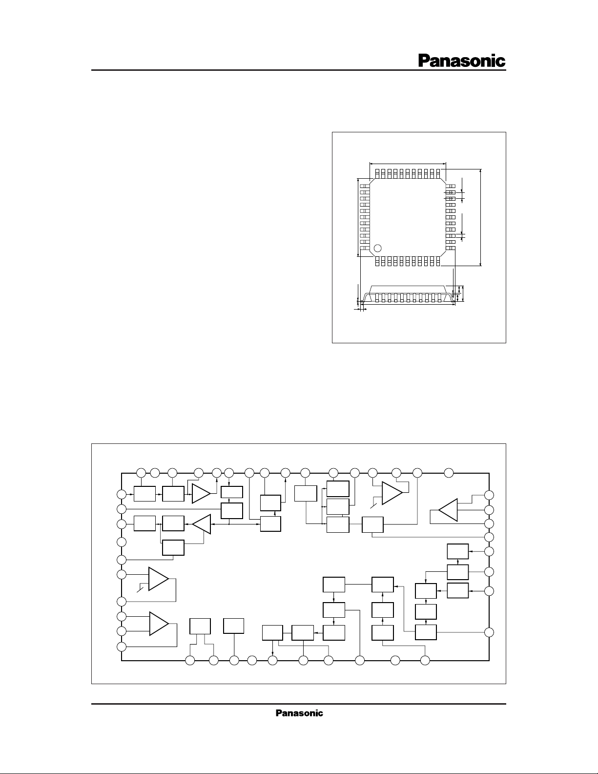
44-Pin QUADFLAT Package (QFP044-P-1010)
12.3±0.4
22
12
– 0.05
+0.1
0.15
0.8
0.35±0.1
0.9±0.25
0.9±0.25
Unit:mm
12.3±0.4
2.0±0.2
■ Block Diagram
V
CC
(DS)
34 33 35 32 31 29 26 28 27 24 4 21 5 6 22 25
Clamp S.H
37
30
ALC
38
DET
GND
36
(DS)
39
41
40
42
43
44
–
+
–
+
ALC
DC
F··B
DC
F·B
–
+
Vref
Chara.
Mix
Chara.
SW
Chara.
Clamp
AGC
OP
CC
(Video)
Mix
Amp
DC
F·B
1114910121331521
AP
Amp
AP
Clamp
Y.
Clamp
AP
Clip
20
19
17
23
16
18
Γ
8
7
AGC
Det.
Y·
Cont
Y·
H.Clip
C.BLK
Mix
Low
Clip
Γ
Γ
ALC
Amp
Clamp
WHD
MIX
Vref
AGC
Flicker
Video
out
Clamp
V.Sync
Mix
Amp
G
Pulse
Sep.
GND GND V
Page 2
■ Absolute Maximum Ratings (Ta=25˚C)
Parameter Symbol Rating Unit
Supply voltage
Supply current
Power dissipation
Operating ambient temperature
Storage temperature
V
CC
I
CC
P
D
T
opr
T
stg
■ Recommended Operating Range (Ta=25˚C)
Parameter Symbol Range
Operating supply voltage range
V
CC
■ Electrical Characteristics (Ta=25˚C)
Parameter minCondition typ max UnitSymbol
OB control (1)
OB control (2)
AGC amp gain (1)
AGC amp gain (2)
ALC DET output
Γ circuit gain (1)
Γ circuit gain (2)
AGC DET output
AP clip (1)
AP clip (2)
YΓ amp gain
Supply current (1)
Supply current (2)
CP1 pulse separation level
WHD pulse separation level
WBL pulse separation level
CP2 pulse separation level
BLK pulse separation level
V
V
G
G
V
GΓ
GΓ
V
AGC/DET
G
G
GYΓ
V
V
V
V
V
OB1
OB2
AGC1
AGC2
ALC
CL1
CL2
I
25
I
33
CP1
WHD
WBL
CP2
BLK
1
2
=5V
V
CC
VCC=5V
V
=5V
CC
V
=5V
CC
V
=5V
CC
V
=5V
CC
=5V
V
CC
V
=5V
CC
V
=5V
CC
V
=5V
CC
V
=5V
CC
V
=5V
CC
V
=5V
CC
V
=5V
CC
V
=5V
CC
V
=5V
CC
V
=5V
CC
V
=5V
CC
5.5
54
280
–20 to +75
–55 to +125
4.5V to 5.3V
35 55 75 mV
–85
130
–65
170
16 19 22 dB
500 600 700 mV
660 800 940 mV
550 mV
400 480 560 mV
0.9 1.1 1.4 V
–10 dB
1.1 1.3 1.5 V
26.5 31 35.5 mA
9.5 14 18.5 mA
3.4 3.8 4.2 V
2.15 2.55 2.95 V
0.4 0.8 1.2 V
3.1 3.5 3.9 V
0.6 1 1.4 V
–45
210
mA
mW
V
˚C
˚C
PP
mV
PP
mV
PP
PP
PP
PP
PP
PP
PP
Page 3

■ Applica tion Circuit
Sig IN
5V
PED Setting
0.047µF
For Iris Driving
Buffer
–
100pF
DS
10kΩ
1kΩ
1kB
10kB
DC
F·B
AP
Clamp
AP Clip
Y·
Γ
Clamp
Vref (–1.8V)
–
+
3kΩ
to
6kΩ
5V
DL
23
0.047µF
Vref
5V
20
DL
19
0.047µF
17
16
0.1µF
5V
18
8
0.047µF
9V
2.4kΩ
22kΩ
4.7kΩ
Vcc
CP (DS) SP3
34
33 35 32 29 27 21
Clamp
37
S.H
R Amp
30
+
ALC
38
DET
36
ALCT
DC
F·B
390kΩ
ALC
Amp
–
+
1kΩ LPF
4.7kΩ
31
Clamp
WHD
MIX
39
5V
41
ALC Op-amp.
–
47µF
Vref
1kΩ
1.2kΩ
26
–
+
5V
AGC
Flicker
47µF
–
+
AGC
5V
30kΩ
24 4
Clamp
Auto
0.047µF
Manual
10kB
33kΩ
4.7µF
AGC
Det
Y·
Cont
Y·
–
+
Γ
Γ
12kΩ
1.6MΩ
528 6 22
AGC
Ope-amp.
–
+
AP Amp.
+
40
42
43
44
Vref
–
+
ALC Op-amp.
H Clip
C. BLK
MIX
Chara.
MIX
Chara.
SW
MIX
Amp
CP2
BLK
CP1
WHD
WBLK
10kΩ
10kΩ
10kΩ
Pulse
Sep.
1 2 15 3
CP2
BLK
WBLK
Vref
+
–
CP1
47µF
WHD
Video
Out
Sig out
V SYNC
MIX
10 9 14 25
13
12
Sync
4kΩ
0V
12kΩ
5V
5V
Low
Clip
PED
5V
Chara.
Clamp
11
V
DC F·B
(Video)
CC
7
V
CC
5V
0.047µF
5V
Page 4

■ Pin Descriptions
Pin No.
1
2
Pin name Typ. waveform
Pulse input 1
Pulse input 2
3.3V
1.6V
5V
2.5V
Pin No.
CP2
5V
BLK
CP1
WHD
WBL
23
24
Pin name Typ. waveform
DC control
γ input
800mV
1.8V
PP
3
GND
4
AGC DET
5
AGC op. amp. input
6
AGC op. amp. output
7
DC control
8
Yγ input
9
PED
10
GND
11
Character input
12
SYNC input
13
Video output
14
V
CC
15
V
ref
(Video)
25
V
CC
480mV
PP
–
320mV
PP
1.8V
2V
DC
1.8V
2.5V
Clamp
PP
IN
Flicker control
26
AGC output
27
AGC control
28
AGC input
29
PED setting
30
DS amp. output
31
DC output
32
V
33
34
35
36
37
(DS)
CC
Clamp pulse input
Sample hold pulse input
GND (DS)
DS input
Open 1.8V
1.8V
1.8V
0V
0V
Reset pulse
800mV
PP
250mV
PP
250mV
PP
100ns
5V
100ns
5V
Signal
16
Aperture input
17
Aperture amp. output
18
Aperture clip
19
Aperture amp. input +
20
Aperture amp. input –
21
γ control
22
γ output
2.5V
350mV
1.8V
580mV
ALC DET
38
DC control
39
ALC op. amp. output
40
ALC op. amp. input –
41
ALC op. amp. input –
42
ALC op. amp. input +
43
PP
ALC op. amp. output
44
PP
 Loading...