

Page 1
AN2018S
p
Unit
Correlated Double Sampling IC
■ Overview
The AN2018S is used to reduce noise in CCD image sensor output signal. It performs correlated doublesampling on image signal sent from a CCD sensor to
output clearer image signal.
■ Features
• Operating on low voltage (VCC=4.8V), consuming
little current (ICC=12.7mA typ.)
• Including a high-speed sampling circuit responding
to 510-830H CCD
• 6dB or 9dB fixed gain
• 83-dB high S/N-ratio (at 6dB output)
0.41.27
0.4±0.25
0.1±0.1
0.3
4.2±0.3
6.5±0.3
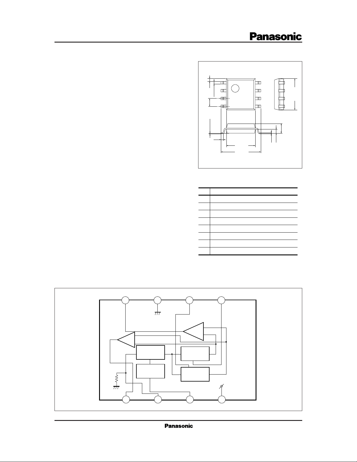
8-Pin SOP Package (SOP008-P-0225)
■ Pin Descriptions
Pin No.
CDS output (9dB)
1
2
Blanking pulse input
CCD signal input
3
4
V
CC
5
Sampling pulse input (2)
6
Sampling pulse input (1)
7
GND
8
CDS output (6dB)
Pin name
0.15
:mm
5.0±0.3
1.5±0.2
0.65
■ Block Diagram
6dB OUT GND SP1 SP2
8765
+
+
9dB
–
BLK
50kΩ
BIAS
1234
9dB OUT BLK SIG.IN V
6dB
–
S / H
S / H
CC
Page 2
■ Absolute Maximum Ratings
Parameter Symbol Rating Unit
Supply voltage
Supply current
Power dissipation
Operating ambient temperature
Storage temperature
Note 1)
Note 1)
V
CC
I
CC
P
D
T
opr
T
stg
5.5
18
99
–20 to +70
–55 to +125
Note 1) Ta=25˚C except operating ambient temperature and storage temperature.
■Recommended Operating Range (Ta=25˚C)
Parameter Symbol Range
Operating supply voltage range
V
CC
4.5V to 5.1V
■ Electrical Characteristics (VCC=4.8V, Ta=25±2˚C)
Parameter minCondition typ max UnitSymbol
Supply current
Terminal voltage pin (3)
Terminal voltage pin (8)
Terminal voltage pin (1)
6dB amp. gain
9dB amp. gain
AMP frequency characteristics
AMP common mode
rejection ratio
*
Sampling pulse threshold (1)
Sampling pulse threshold (2)
Blanking pulse high level
I
CC
V
3
V
8
V
1
G
1
G
2
*
f
C
CMR
V
TH1
V
TH2
V
THB
Note) The value in the above characteristics is not a guaranteed value, but reference one on design.
*
The characteristics are of the amplifier itself.
4.8V
V
CC
=
4.8V
V
CC
=
Pint, y=4.8V
4.8V
V
CC
=
Pint, y=4.8V
4.8V
V
CC
=
Pint, y=4.8V
Input level=300mV
Input level=300mV
4.8V
V
CC
V
V
V
V
V
V
V
=
100mV
3
=
CC
=
100mV
3
=
CC
=
CC
=
CC
=
300mV
3
=
4.8V
4.8V
4.8V
4.8V
P–P
P–P
P–P
10MHz
10MHz
P–P
P–P
9.2
2.48
1.30
1.25
5.0
7.8
0.8
0.8
3.5
12.7
2.63
1.60
1.55
6.0
9.0
3.0
–
35
–
1.5
1.5 2.2
V
mA
mW
˚C
˚C
16.2 mA
1.90
1.85
7.0
10.2
dB
dB
dB
dB
2.2
V2.78
V
V
V
V
V
Page 3

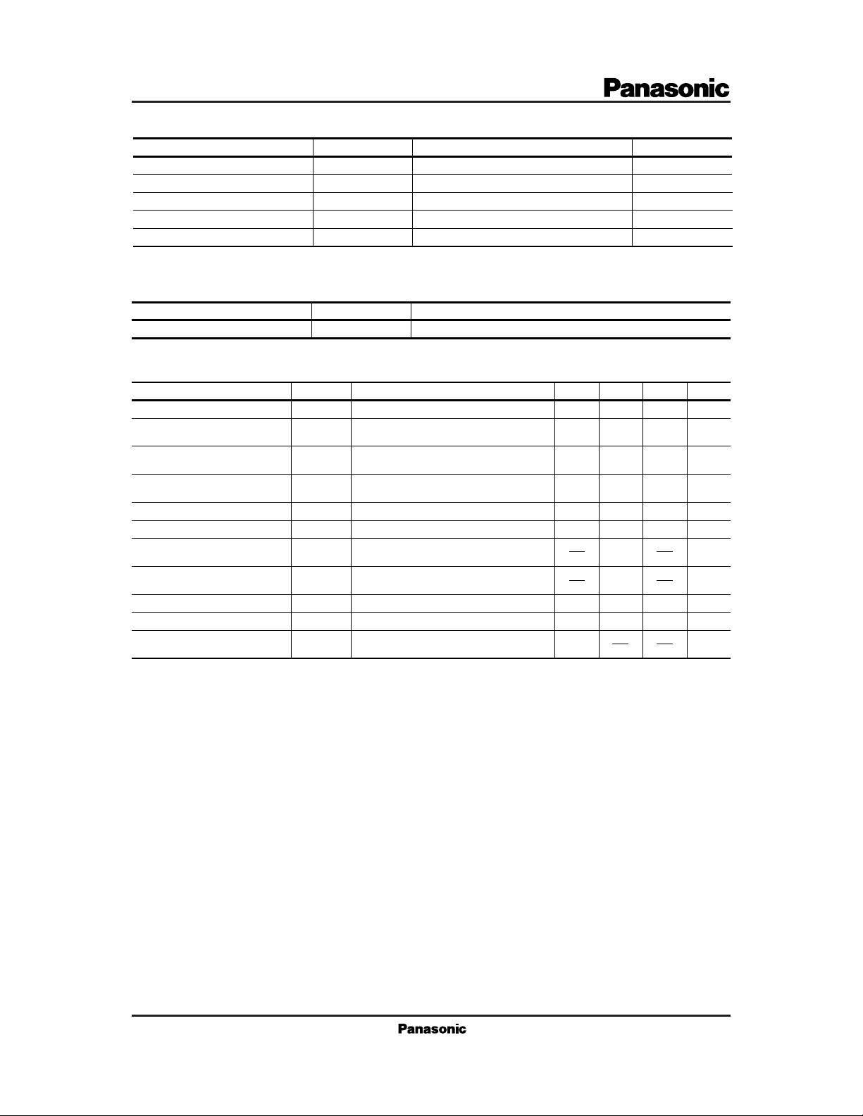
■ Pin Descriptions
Pin No.
Pin name Equivalent circuit
DC voltage (V
CC=
5V)
Description
V
(4)
CC
1 9dB OUT
2
BLK
SIG.IN
3
4
V
CC
Black level:
1.55V
H 3.5V
L 0.5V
Black level:
2.6V
4.8V
8
1
50kΩ
3
50µA
1kΩ
1kΩ
75
µA
Ω
200
1kΩ 58kΩ
GND (7)
33kΩ
63kΩ
38kΩ
500Ω
(4)
V
CC
GND (7)
(4)
V
CC
GND (7)
•9-dB-amp. output CDS signal
•Typical 1.55V DC output
•90-Ω output impedance
•Blanking (Hclear) pulse input (from
an AN2145 series only)
•Active high
•3.0V threshold voltage
•50kΩ input impedance
•Grounded or left open when not
used
•CCD signal input
•CCD signal must be input through
a capacitor.
•The capacitor should preferably be
0.022µF.
•2.6V typ. bias voltage
•Supply voltage
5
6
7
8
SP2
SP1
GND
6dB OUT
H 2.2V
L 0.8V
H 2.2V
L 0.8V
Black level:
1.6V
5
6
Same as for Pinq.
300µA
Ω
1k
300µA
1kΩ
28kΩ
20kΩ
28kΩ
20kΩ
(4)
V
CC
GND (7)
(4)
V
CC
GND (7)
•Sample-hold pulse input
•Active high
•1.5V threshold voltage
•Sampling pulses are input in synchronization with the video timing
of CCD signal at Pine.
•Sample-hold pulse input
•Active high
•1.5V threshold voltage
•Sampling pulses are input in synchronization with the feed-through
timing of CCD signal at Pine.
•Ground
•6-dB-amp. output CDS signal
Note) The above characteristics value, measured at VCC=5V, is not a guaranteed value, but reference one on design.
 Loading...