Page 1

AN-1149
APPLICATION NOTE
MEMORY
V
DD
MICROPROCESSOR
LCD DISPLAY
BUCK
REGULATOR
ADP2139
SENSOR
BATTERY
Li-Ion
1.8V
3.6V
3.3V
RF PA
BUCK-BOOST
REGULATOR
ADP2503
BUCK-BOOST
REGULATOR
ADP2504
3.0V TO 4.2V
10542-001
One Technology Way • P. O. Box 9106 • Norwood, MA 02062-9106, U.S.A. • Tel: 781.329.4700 • Fax: 781.461.3113 • www.analog.com
How to Apply DC-to-DC Step-Down/Step-Up (Buck/Boost) Regulators
by Ken Marasco
INTRODUCTION
DC-to-DC switching converters are used to change one dc
voltage to another efficiently. High efficiency dc-to-dc
converters come in three basic topologies: step-down (buck),
step-up (boost), and step-down/step-up (buck/boost).
The buck converter is used to generate a lower dc output
voltage, the boost converter is used to generate a higher dc
output voltage, and the buck/boost converter is used to generate
an output voltage less than, greater than, or equal to the input
voltage.
This application note focuses on how to successfully apply
buck/boost dc-to-dc converters. Buck and boost converters are
described individually in the AN-1125 Application Note, How
to Apply DC-to-DC Step-Down (Buck) Regulators, and the
AN-1132 Application Note, How to Apply DC-to-DC Step-Up
(Boost) Regulators.
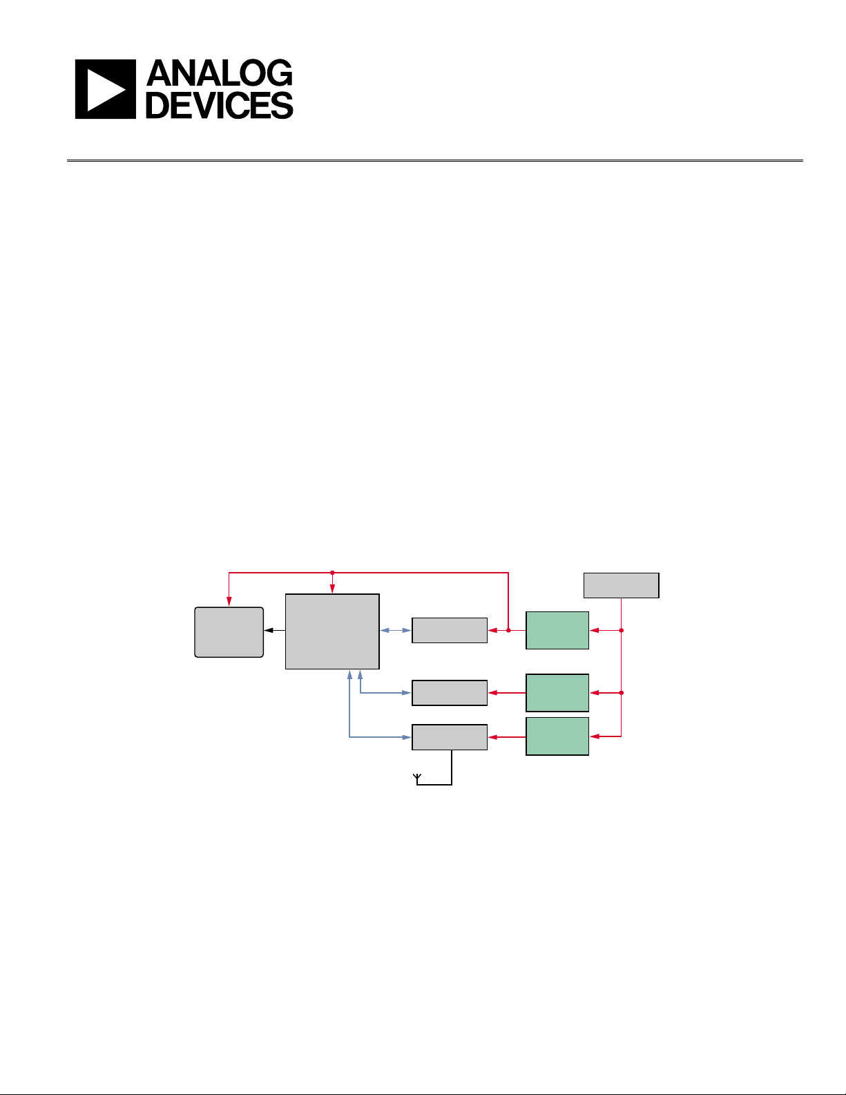
Figure 1 shows a typical low power system powered from a
single-cell lithium ion (Li-Ion) battery. The battery’s usable
output varies from about 3.0 V when discharged to 4.2 V when
fully charged. The system ICs require 1.8 V, 3.3 V, and 3.6 V for
optimum operation. Whereas the lithium ion battery starts at
4.2 V and ends at 3.0 V, a buck/boost regulator can supply a
constant 3.3 V, and a buck regulator or low dropout (LDO)
regulator can supply 1.8 V, as the battery discharges. A buck
regulator or LDO can conceivably be used for the 3.3 V while
the battery voltage is above 3.5 V, but the system would cease to
operate when the battery voltage drops below 3.5 V. Allowing
the system to be turned off prematurely reduces the system’s
operating time before the battery must be recharged.
Figure 1. Typical Low Power Portable System
Rev. 0 | Page 1 of 8
Page 2

AN-1149 Application Note
TABLE OF CONTENTS
Introduction ...................................................................................... 1
Revision History ............................................................................... 2
Buck/Boost Regulators ..................................................................... 3
Buck/Boost Regulators Improve System Efficiency ..................... 5
Buck/Boost Regulator Key Specifications and Definitions ......... 6
Output Voltage Range Options ................................................... 6
Ground or Quiescent Current .................................................... 6
Shutdown Current ........................................................................ 6
REVISION HISTORY
4/12—Revision 0: Initial Version
Soft Start .........................................................................................6
Switching Frequency .....................................................................6
Thermal Shutdown (TSD) ...........................................................6
Buck/Boost DC-to-DC Switching Converters Operate at
MHz ................................................................................................7
Conclusion..........................................................................................8
References .......................................................................................8
Rev. 0 | Page 2 of 8
Page 3

Application Note AN-1149
V
V
V
BUCK/BOOST REGULATORS
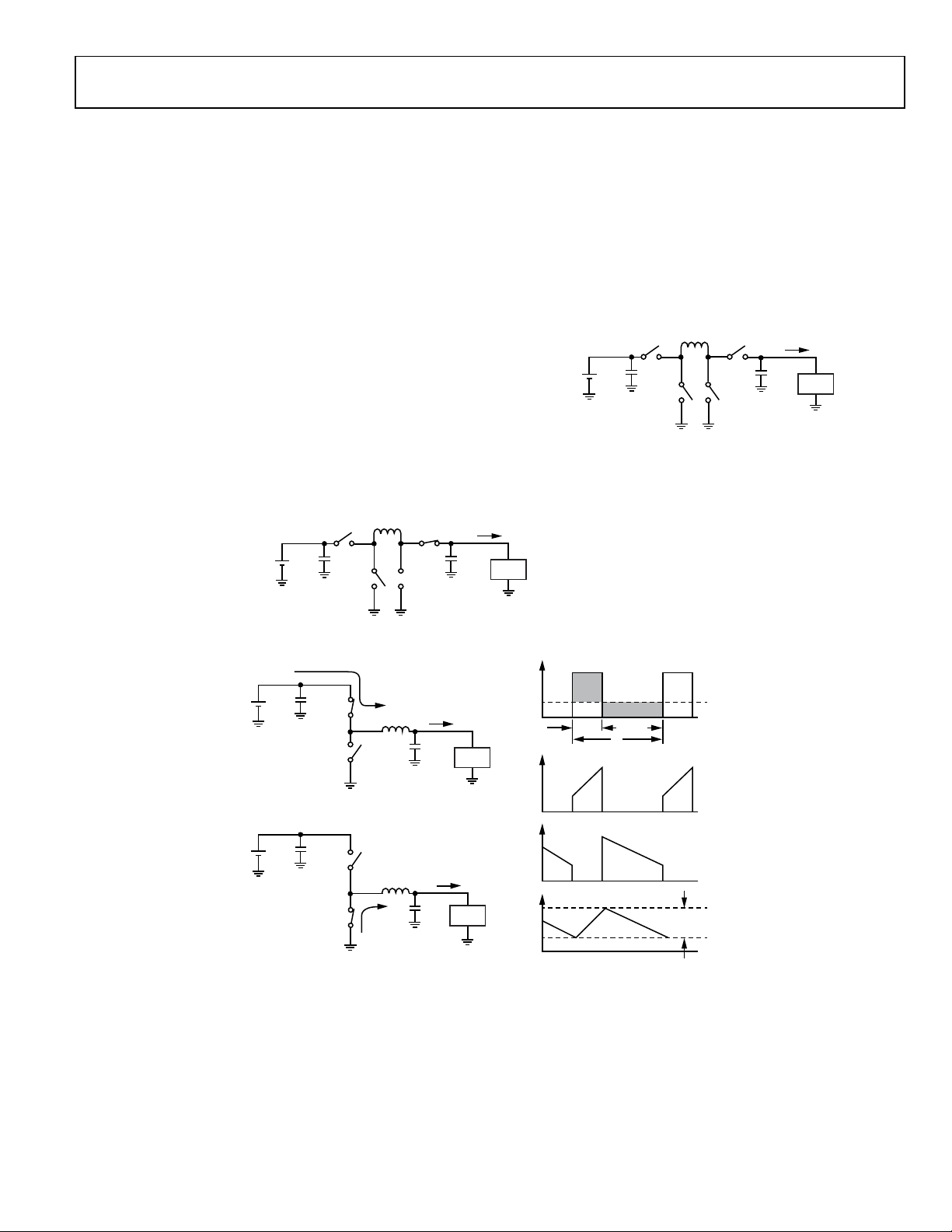
Buck/boost regulators contain four switches, two capacitors,
and an inductor, as shown in Figure 2. Current low power, high
efficiency buck/boost regulators reduce losses and improve
efficiency by actively operating only two of the four switches
when operating in buck or boost mode.
When V
is greater than V
IN
, Switch C is open and Switch D
OUT
is closed. Switch A and Switch B operate as in a standard buck
regulator, as shown in Figure 3.
When V
is less than V
IN
, Switch B is open and Switch A is
OUT
closed. Switch C and Switch D operate as in a boost regulator,
as shown in Figure 4. The most difficult operating mode is
when V
is in the range of V
IN
± 10% and the regulator enters
OUT
the buck/boost mode. In buck/boost mode, the two operations,
buck and boost, take place during a switching cycle. Care must
be taken to reduce losses, optimize efficiency, and eliminate
instability due to mode switching. The objective is to maintain
voltage regulation with minimal current ripple in the inductor
to guarantee good transient performance.
L
+
V
IN
–
A
C
IN
BC
D
I
C
OUT
At high load currents, the buck/boost uses voltage or currentmode, fixed frequency pulse-width modulation (PWM) control
for optimal stability and transient response. To ensure the
longest battery life in portable applications, a power save mode
reduces the switching frequency under light load conditions.
For wireless and other low noise applications where variablefrequency power save mode may cause interference, the
addition of a logic control input to force fixed frequency PWM
operation under all load conditions is included.
L
+
IN
–
A
C
IN
BC
Figure 2. Buck/Boost Converter Topology
I
LOAD
D
C
OUT
LOAD
V
OUT
LOAD
LOAD
V
OUT
10542-002
IN BUCK MODE SWITCH C IS O PEN AND SWIT CH D IS CLOSED.
I
+
IN
–
TYPICAL BUCK
OPERATION
+
IN
–
C
IN
PWM ON
C
IN
PWM OFF
A
A
V
SW
B
A
V
SW
B
I
B
I
LOAD
L
C
I
L
C
OUT
LOAD
OUT
LOAD
LOAD
V
OUT
V
OUT
Figure 3. Buck Mode When V
V
I
LOAD
PWM
OUT
MODULATIO N
t
OFF
T
∆I
LOAD
V
OUT
10542-003
SW
t
ON
I
A
I
B
> V
IN
Rev. 0 | Page 3 of 8
Page 4

AN-1149 Application Note
V
V
+
C
V
IN
IN
–
L
A
BC
I
LOAD
V
D
C
OUT
OUT
LOAD
IN BOOST MODE SWIT CH B IS OPEN AND SWITCH A IS CLOSE D.
PWM
MODULATION
t
ON
T
V
OUT
V
IN
t
OFF
+
C
IN
IN
–
PWM ON
TYPICAL BOOST
OPERATION
+
C
IN
–
PWM OFF
V
SW
I
ON
L
D
V
SW
C
I
IN
OFF
L
V
SW
C
I
LOAD
C
OUT
I
D
C
LOAD
OUT
LOAD
LOAD
V
OUT
I
ON
I
OFF
V
OUT
I
LOAD
∆I
Figure 4. Boost Mode When V
LOAD
< V
IN
OUT
10542-004
Rev. 0 | Page 4 of 8
Page 5

Application Note AN-1149
BUCK/BOOST REGULATORS IMPROVE SYSTEM EFFICIENCY
A large number of the portable systems in use today are powered by a single-cell rechargeable Li-Ion batte r y. The battery
starts from a fully charged 4.2 V and slowly discharges down to
3.0 V. When the battery output drops below 3.0 V, the system
turns off to protect the battery from damage due to extreme
discharging. When a low dropout regulator is used to generate a
3.3 V rail, the system shuts down at
V
= V
IN MIN
OUT
+ V
= 3.3 V + 0.2 V = 3.5 V
DROPOUT
using only 70% of the battery’s stored energy. However, using a
buck/boost regulator such as the ADP2503 or ADP2504 enables
the system to continue operating down to the minimum practical battery voltage. The ADP2503 and ADP2504 (see the
Buck/Boost DC-to-DC Switching Converters Operate at 2.5 MHz
section) are high efficiency, low quiescent current, 600 mA and
1000 mA, step-down/step-up (buck/boost) dc-to-dc converters
that operate with input voltages greater than, less than, or equal
to the regulated output voltage. The power switches are internal,
minimizing the number of external components and thus
reducing printed circuit board (PCB) area. This approach
allows the system to operate all the way down to 3.0 V, using
most of the battery’s stored energy and increasing the system’s
operating time before a battery recharge is required.
To save energy in portable systems, various subsystems, such as
the microprocessor, display backlighting, and power amplifiers,
when not in use, are frequently switched between full power-on
and sleep mode, which can induce large voltage transients on
the battery supply line. These transients can cause the battery’s
output voltage to briefly drop below 3.0 V and trigger the low
battery warning, causing the system to turn off before the battery is completely discharged. The buck/boost solution tolerates
voltage swings as low as 2.3 V, helping to maintain the system’s
potential operating time.
Rev. 0 | Page 5 of 8
Page 6

AN-1149 Application Note
BUCK/BOOST REGULATOR KEY SPECIFICATIONS AND DEFINITIONS
OUTPUT VOLTAGE RANGE OPTIONS
Buck/boost regulators are available with specified fixed output
voltages or in an option that allows the output voltage to be
programmed via an external resistance divider.
SOFT START
It is important to have a soft start function that ramps the
output voltage in a controlled manner to prevent excessive
output voltage overshoot at startup.
GROUND OR QUIESCENT CURRENT
Ground current is the dc bias current not available for the load
(I
). The lower the IQ is, the better the efficiency, but IQ can be
Q
specified under many conditions, including switched off, zero
load, pulse frequency modulation (PFM), and pulse-width
modulation (PWM) operation. It is, therefore, best to examine
operating efficiency at specific operating voltages and load
currents when determining the best boost regulator for the
application.
SHUTDOWN CURRENT
Shutdown current is the input current consumed when the
enable pin has been set to off. Low I
standby times when a battery-powered device is in sleep mode.
During logic controlled shutdown, the input is disconnected
from the output and draws less than 1 μA from the input source.
is important for long
Q
SWITCHING FREQUENCY
Low power buck/boost converters generally operate between
500 kHz and 3 MHz. Higher switching frequencies allow the
use of smaller inductors and reduce the required PCB area, but
efficiency is decreased by approximately 2% for every doubling
of the switching frequency.
THERMAL SHUTDOWN (TSD)
If the junction temperature rises above the specified limit,
the thermal shutdown circuit turns the regulator off. Consistently high junction temperatures can be the result of high
current operation, poor circuit board cooling, and/or high
ambient temperature. The protection circuit includes hysteresis
so that, after thermal shutdown, the device does not return to
normal operation until the on-chip temperature drops below
the preset limit.
Rev. 0 | Page 6 of 8
Page 7

Application Note AN-1149
BUCK/BOOST DC-TO-DC SWITCHING CONVERTERS OPERATE AT 2.5 MHZ
The ADP2503 and ADP2504 are high efficiency, low quiescent
current step-up/step-down dc-to-dc converters that can operate
at input voltages greater than, less than, or equal to the regulated output voltage. The power switches and synchronous
rectifiers are internal to minimize external part count. At high
load currents, they use a current-mode, fixed frequency pulsewidth modulation (PWM) control scheme for optimal stability
and transient response. To ensure the longest battery life in
portable applications, the devices have an optional power save
mode that reduces the switching frequency under light load
conditions. For wireless and other low noise applications where
a variable frequency power save mode may cause interference,
the logic control input sync forces fixed frequency PWM
operation under all load conditions.
The ADP2503 and ADP2504 can run from input voltages
between 2.3 V and 5.5 V, allowing a single lithium or lithium
polymer cell, multiple alkaline or NiMH cells, PCMCIA, USB,
and other standard power sources. Various fixed output options
are available, or, using the adjustable model, the output voltage
can be programmed through an external resistor divider.
Compensation is internal to minimize the number of external
components.
Rev. 0 | Page 7 of 8
Page 8

AN-1149 Application Note
©2012 Analog Devices, Inc. All rights reserved. Trademarks and
CONCLUSION
Low power buck/boost regulators with proven performance and
in-depth support take the worry out of designs using switching
dc-to-dc converters. In addition to a comprehensive ADP2503/
ADP2504 data sheet with design calculations available, the
ADIsimPower™ design tool simplifies the task for the end user.
Regulator selection guides, data sheets, and application notes
can be found at www.analog.com/power-management.
For help, visit EngineerZone™ at http://ez.analog.com, or phone
or email an application engineer at Analog Devices.
REFERENCES
Marasco, Ken. AN-1125 Application Note. How to Apply DC-to-
DC Step-Down (Buck) Regulators. Analog Devices, Inc., 2011.
Marasco, Ken. AN-1132 Application Note. How to Apply DC-to-
DC Step-Up (Boost) Regulators. Analog Devices, Inc., 2011.
Marasco, Ken. AN-1072 Application Note. How to Successfully
Apply Low-Dropout Regulators. Analog Devices, Inc., 2010.
http://www.analog.com/ADIsimPower
http://www.analog.com/power-management
http://www.analog.com/switching_controllers
http://www.analog.com/switching-regulators
registered trademarks are the property of their respective owners.
AN10542-0-4/12(0)
Rev. 0 | Page 8 of 8
 Loading...