

Page 1
AN-1006
APPLICATION NOTE
One Technology Way • P. O . Box 9106 • Norwood, MA 02062-9106, U.S.A. • Tel : 781.329.4700 • Fax: 781.461.3113 • www.analog.com
Using the EVAL-ADUSB2EBZ
by Brett Gildersleeve
INTRODUCTION
The EVAL-ADUSB2EBZ features USB-to-I2C and SPI conversion.
It is compatible with 1.8 V and 3.3 V target devices and allows
for SigmaStudio™ integration for most SigmaDSP® processors.
Its on-board power regulators are capable of supplying the
target board, and it features a standard Aardvark-compatible
programming header. The EVAL-UDSUB2EBZ provides SPI
control of up to five slave devices with a low profile surfacemount USB miniature Type B connector, and it allows for plugand-play operation.
The EVAL-ADUSB2EBZ is ideal for downloading code
and register settings to SigmaDSP processors and codecs
with SigmaStudio. It can also be used for real-time tuning
of SigmaDSP production units with SigmaStudio.
GENERAL DESCRIPTION
The EVAL-ADUSB2EBZ, also known as the USBi, is a standalone
communications interface and programmer for SigmaDSPsystems.
It translates USB control commands from SigmaStudio to the I
and SPI communications protocols. The USBi is powered over
the USB cable; therefore, no external power supply is required.
2
C
The ribbon cable and 10-pin header form a bridge to the target
board to connect the communications signals to the target IC.
The ribbon cable also carries 5 V power from the USB hub, which
can be used to power the target board if desired.
The on-board regulators enable both 1.8 V and 3.3 V IOVDD
operation, allowing for increased compatibility with target
devices.
Up to five slave devices can be controlled by the USBi simultaneously. To control multiple SPI devices, additional latch signals
are provided, although they are not connected to the ribbon cable.
The USBi can be used to control SigmaDSP systems in real time
via SigmaStudio, and is capable of programming an EEPROM
in self-boot systems. It is an ideal solution for in-circuit programming and tuning of prototype systems.
The USBi only supports USB 2.0 interfaces; the USBi will not
work with PCs that only support USB Version 1.0 and USB
Version 1.1.
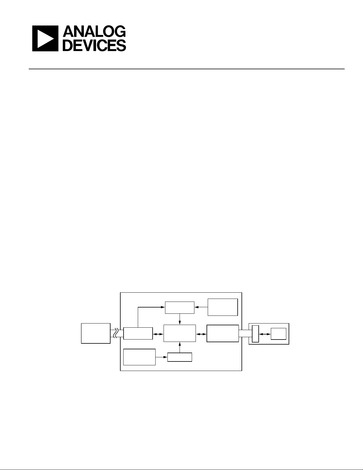
FUNCTIONAL BLOCK DIAGRAM
EVAL-ADUSB2 (USBi)
POWER
REGULATOR
HOST PC
SigmaStudio
USB
CONNECTOR
EEPROM
PROGRAMMING
HEADER
CYPRESS
USB INTERFACE
EEPROM
Figure 1.
Rev. A | Page 1 of 16
1.8V/3.3V
SELECTOR
SWITCH
PROGRAMMING
HEADER
TARGET
BOARD
SIGMA
DSP
08093-001
Page 2

AN-1006 Application Note
TABLE OF CONTENTS
Introduction ...................................................................................... 1
USB Connector ..............................................................................7
General Description ......................................................................... 1
Functional Block Diagram .............................................................. 1
Using the USB Interface with SigmaStudio ................................... 3
Installing the Drivers ................................................................... 3
Adding the USBi to a SigmaStudio Project ............................... 4
Configuring the USBi to Communicate with an IC ................ 4
Configuring the USBi to Communicate with Multiple ICs .... 4
Controlling the USBi .................................................................... 5
Monitoring the USBi .................................................................... 6
Using the USBi to Program a Self-Boot EEPROM .................. 6
Warning ......................................................................................... 6
Circuit Schematics ............................................................................ 7
REVISION HISTORY
4/10—Rev. 0 to Rev. A
Changes to General Description Section .......................................1
Added Warning Section ................................................................... 6
5/09—Revision 0: Initial Version
Power Regulator ............................................................................7
Cypress USB Interface ..................................................................8
Crystal Oscillator Schematic ........................................................8
LEDs ................................................................................................9
EEPROM ........................................................................................9
Target Board Power Switch ..........................................................9
Target Board Programming Header ...........................................9
Evaluation Board Schematics and Artwork ................................ 10
Schematics ................................................................................... 10
Board Layout ............................................................................... 12
Bill of Materials ............................................................................... 13
Rev. A | Page 2 of 16
Page 3
Application Note AN-1006
USING THE USB INTERFACE WITH SIGMASTUDIO
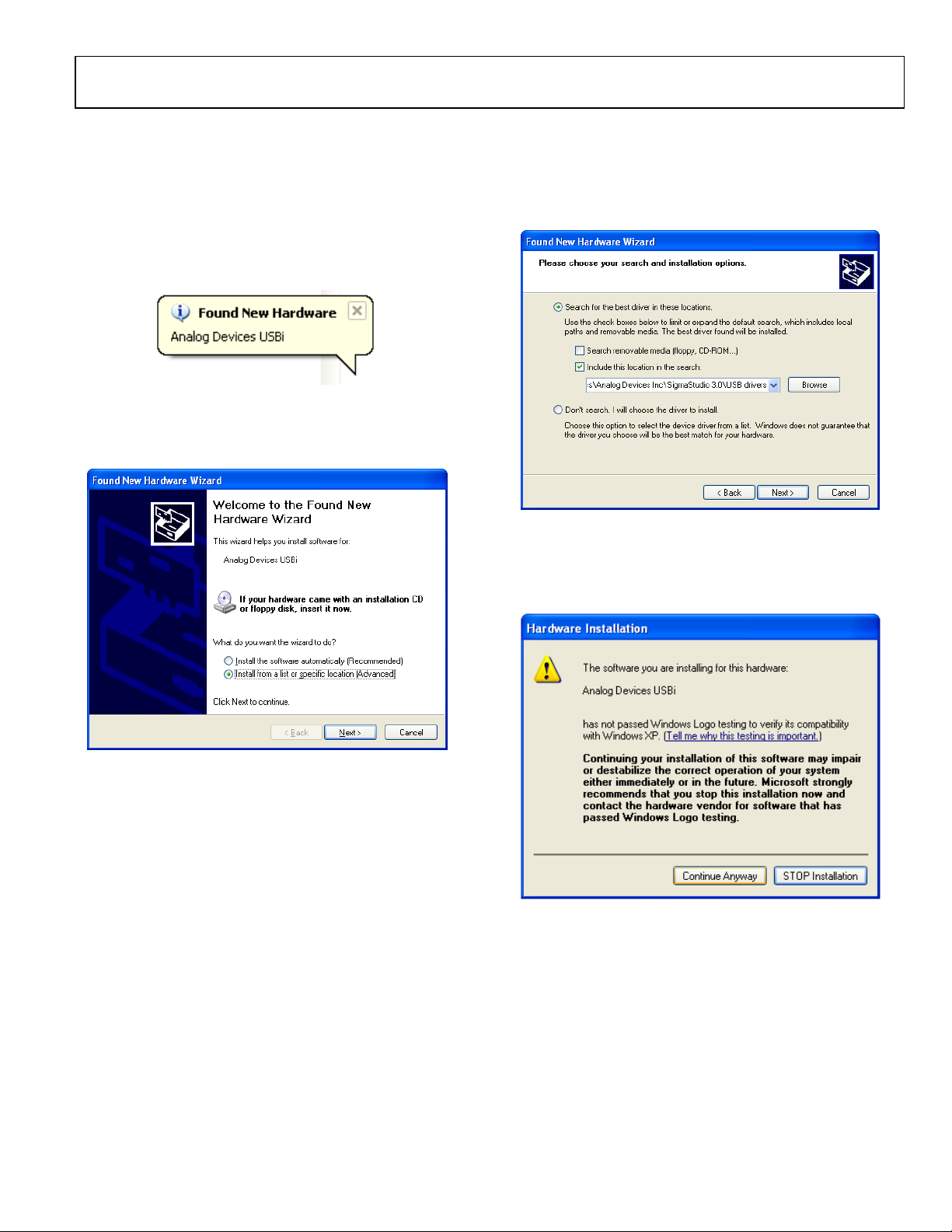
INSTALLING THE DRIVERS
SigmaStudio must be installed to use the USBi. Once
SigmaStudio has been properly installed, connect the USBi to
an available USB port with the included USB cable. At this
point, Windows® XP recognizes the device and prompts the
user to install drivers.
08093-002
Figure 2. Found New Hardware Notification
Select the Install from a list or specific location (Advanced)
option and click Next >.
Click Search for the best driver in these locations, then select
Include this location in the search. Click Browse to find the
SigmaStudio 3.0\USB drivers directory.
Figure 4. Windows Found New Hardware Wizard—Search and
Installation Options
08093-004
Figure 3. Found New Hardware Wizard—Installation
When the warning about Windows Logo testing appears on the
screen, click Continue Anyway.
8093-003
Figure 5. Windows Logo Testing Warning
08093-005
Rev. A | Page 3 of 16
Page 4
AN-1006 Application Note
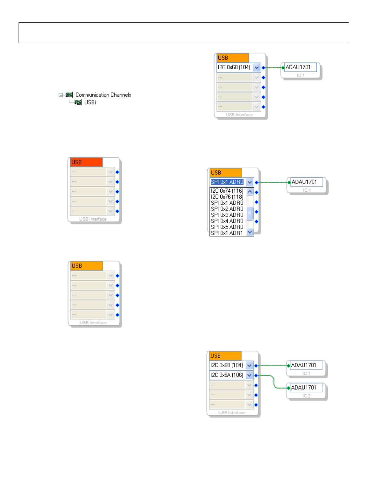
ADDING THE USBi TO A SIGMASTUDIO PROJECT
To use the USBi in conjunction with SigmaStudio, first select it
in the Communication Channels subsection of the toolbox in
the Hardware Configuration tab, and add it to the project space.
8093-006
Figure 6. Adding the USBi Communication Channel
If SigmaStudio cannot detect the USBi on the USB port of the
computer, then the background of the USB label will be red.
This may happen when the USBi is not connected or when the
drivers are incorrectly installed.
08093-009
Figure 9. Connecting the USBi to an IC
To change the communication mode and channel, click the
drop-down box and select the appropriate mode and channel
from the list.
08093-007
Figure 7. USBi Not Detected by SigmaStudio
If SigmaStudio detects the USBi on the USB port of the computer,
the background of the USB label changes to orange.
08093-008
Figure 8. USBi Detected by SigmaStudio
CONFIGURING THE USBi TO COMMUNICATE WITH AN IC
To use the USBi to communicate with the target IC, connect it
by click-dragging a wire between the blue pin of the USBi and
the green pin of the IC. The corresponding drop-down box of
the USBi automatically fills with the default mode and channel
for that IC.
08093-010
Figure 10. Selecting the Communications Mode and Channel
CONFIGURING THE USBi TO COMMUNICATE WITH MULTIPLE ICS
The USBi can communicate with up to five ICs simultaneously.
To communicate with more than one IC, add another IC to the
project and connect it to the next available pin of the USBi.
Multiple Address Operation with I2C
The USBi can support up to four identical devices on the same
bus if the I
dently set to four different addresses, matching the addresses in
the drop-down box in the Hardware Configuration tab of
SigmaStudio.
2
C address pins of the target devices are indepen-
Rev. A | Page 4 of 16
Figure 11. Multiple Address Operation with I
08093-011
2
C
Page 5
Application Note AN-1006
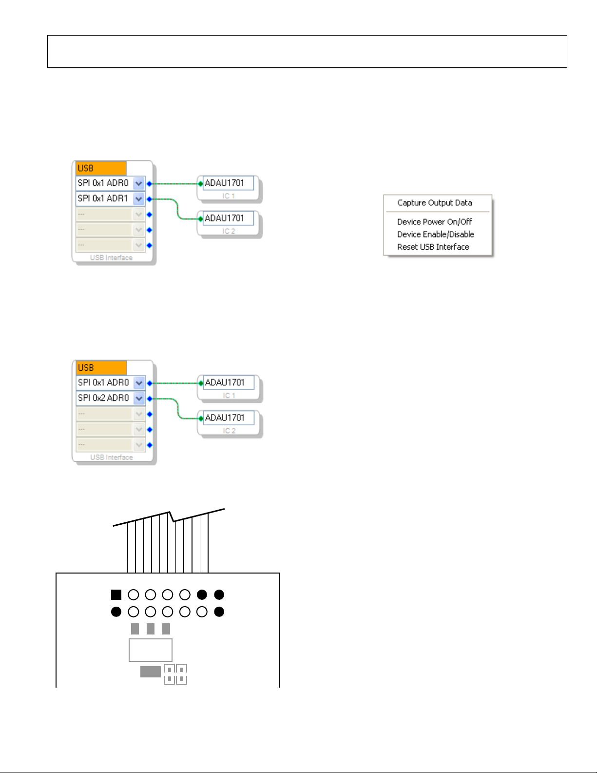
Multiple Address Operation with SPI Combined Multiple Latch and Multiple Address
The USBi can support up to two identical devices on the same
SPI latch if the SPI address pins of the target devices are independently set to two different addresses, matching the addresses in
the drop-down box in the Hardware Configuration tab of
SigmaStudio.
08093-012
Figure 12. Multiple Address Operation with SPI
Multiple Latch Operation with SPI
The USBi can support devices on five different SPI latches.
When multiple latches are used, the additional SPI latch signals
from the USBi that are not connected to the ribbon cable need
to be manually wired to the target.
Operation with SPI
A combination of multiple latch and multiple address schemes
can be used, but the total number of devices cannot exceed five.
CONTROLLING THE USBi
The USBi has several functions for controlling the target hardware.
The control options are accessed in SigmaStudio by right-clicking
on the USB Interface in the Hardware Configuration tab.
8093-015
Figure 15. USBi Control Menu
Capture Output Data
This option accesses the Capture Window, which displays a log
of all communication between the PC and the target IC
(see Figure 1
7).
Device Power On/Off
This option switches the line that supplies power to the target
board. By default, the device power is on.
08093-013
Figure 13. Multiple Latch Operation with SPI
The locations of extended SPI latch signals are shown in Figure 14.
0x02 0x04
0x03
Q1
0x01
0x05
Device Enable/Disable
For supported ICs, selecting this option switches the device to
low power mode.
Reset USB Interface
This function performs a software reset of the USB driver, and
causes the Cypress USB microcontroller to reload its firmware.
R12
Figure 14. Extended SPI Latch Signal Pinout (Bottom View of Board)
R11
08093-014
Rev. A | Page 5 of 16
Page 6

AN-1006 Application Note
MONITORING THE USBi
Using the Capture Window, it is possible to view all outgoing
communications transfers from the PC to the target IC. For
each write, the write mode, time of write, cell name (if applicable), parameter name, address, value, data (in decimal and
hexadecimal), and byte length are shown.
For block writes where more than one memory location is
written, only the first location is shown. The expand/collapse
button in the leftmost column allows the user to view the full
data write.
WARNING
The USBi has an EEPROM on the I2C bus at Address 0x51, which
it uses to indicate its Vendor ID and Product ID to the PC, as
well as boot its internal program. You should avoid having any
other EEPROMs in your system design at this address. This
EEPROM is not write-protected; therefore, if you attempt to
write to Address 0x51, you will overwrite the USBi's onboard
EEPROM, and the USBi will cease to function. The USBi cannot be
reprogrammed without returning the board to Analog Devices.
Most EEPROMs are set to Address 0x51 by setting its pins A0 = 1
and A1 = A2 = 0.
USING THE USBi TO PROGRAM A SELF-BOOT EEPROM
After compiling a project, the registers and RAM contents
can be written to a target EEPROM for self-boot. To use this
functionality, an EEPROM IC must be connected to the USBi
in the Hardware Configuration window. After verifying that
the EEPROM write protect pin is disabled on the target board,
right-click the target IC (SigmaDSP), and select Write L a t e st
Compilation to E2PROM.
Figure 16. Writing to the Self-Boot EEPROM
08093-017
08093-016
Figure 17. Output Capture Window
Rev. A | Page 6 of 16
Page 7

Application Note AN-1006
CIRCUIT SCHEMATICS
USB CONNECTOR
The connection between the host PC and the Cypress USB
interface device is via a standard USB cable that carries D+ and
D− signals for data communications, a 5 V power supply, and
ground. The D+ and D− lines are a one-wire communication
interface carried by half-duplex differential signals on a twisted
pair. The clock is embedded in the data using the nonreturn-tozero inverted (NRZI) line code. These signal lines connect
directly to pins on the Cypress USB interface.
POWER REGULATOR
The Cypress USB Interface I/O ports are capable of operating in
both 1.8 V and 3.3 V modes, depending on the target device in
the system. Two regulators, one for 5 V to 3.3 V regulation and
the other for 5 V to 1.8 V regulation, run simultaneously when
the board is powered. A switch (S1) is provided to easily switch
the IOVDD supply between the two regulators. LED D4 provides
visual feedback that the board is being supplied with 5 V power
from the PC USB port.
A surface-mounted USB miniature Type B jack was selected for
its low profile and increasing ubiquity in consumer electronics.
5V0DD
1
VCC
2
J3
D–
USB-MINI-B-SMD
GND
3
D+
4
Figure 18. USB Connector Schematic
5V0DD
D4
Red Diffused
R10
475R
+
C22
15uF
DMINUS
DPLUS
C21
1.0uF
C20
1.0uF
08093-018
ADP1711AUJZ-3.3-R7
1
IN5OUT
3
EN
BYP
GND
2
U8
ADP1711AUJZ-1.8-R7
1
IN5OUT
3
EN
BYP
GND
2
U7
10nF
4
4
C16
C18
10nF
The position of switch S1 should not be changed when the
board is connected to the USB bus.
3V3DD
+
C19
C14
1.0uF
10uF
IOVDD
C17
1.0uF
1V8DD
+
C13
10uF
3V3DD1V8DD
S1
3
2
1
SPDT
TP1
08093-019
Figure 19. Power Regulator Schematic
Rev. A | Page 7 of 16
Page 8

AN-1006 Application Note
CYPRESS USB INTERFACE
The Cypress USB interface is the core of the system, including
all of the necessary functionality to convert USB commands
into corresponding I
2
C or SPI read/write transfers, and acts as a
FIFO to route data between the host PC and the target device.
CRYSTAL OSCILLATOR SCHEMATIC
The Cypress USB interface is its own clock master, and the board
includes a crystal oscillator circuit with a 24 MHz piezoelectric
crystal resonator to provide stability to the oscillator circuit.
The crystal resonator is driven in parallel by the XTALOUT
and XTALIN pins of the Cypress USB interface.
IOVDD
1DD8V3DD3V
Figure 20. Crystal Oscillator Schematic
IOVDD
Local to 68053
C11
22pF
24.000MHz
C27
22pF
Y1
08093-021
C11
22pF
24.000MHz
C27
22pF
Y1
DMINUS
USB_CLK
DPLUS
SCL
SDA
IOVDD
100k
+
C9
0.10uF
VCC_IO
VCC_IO
VCC_D
PA0/INT0
PA1/INT1
PA2/SLOE
PA3/WU2
PA4/FIFOADR0
PA5/FIFOADR1
PA6/PKTEND
PA7/FLAGD/SLCS
PB0/FD[0]
PB1/FD[1]
PB2/FD[2]
PB3/FD[3]
PB4/FD[4]
PB5/FD[5]
PB6/FD[6]
PB7/FD[7]
PD0/FD[8]
PD1/FD[9]
PD2/FD[10]
PD3/FD[11]
PD4/FD[12]
PD5/FD[13]
PD6/FD[14]
PD7/FD[15]
GND
GND
GND
4A4B4C
7D
G
1
U3
VCC_A
8G
6G
8F
7F
6F
8C
7C
6C
3H
4F
4H
4G
5H
5G
5F
6H
8A
7A
6B
6A
3B
3A
3C
2A
GND
GND
8D
C6
0.10uF
2D
5A
5B7E8E5C
AVCC1DAVCC
VCC_IO
2E
DPLUS
1E
DMINUS
3F
SCL
3G
SDA
1A
RDY0/SLRD
1B
RDY1/SLWR
7H
CTL0/FLAGA
7G
CTL1/FLAGB
8H
CTL2/FLAGC
R15
2B
CLKOUT
2G
C1
1.0uF
2C
1C
7B
8B
IFCLK
XTALOUT
XTALIN
WAKEUP
RESET
49R9
R5
VCC_IO
CYPRESS_CY7C68053_56BAXI
AGND
AGND
GND
GND
2F
1F
1H
2H
GND
3V3DDIOVDD
475R
R6
USB_PWR_ON
C8
0.10uF
C10
0.10uF
CDATA
COUT
CLATCH2
CLATCH3
CLATCH4
CLATCH5
CCLK
C12
0.10uF
C15
15uF
10k0
R1
C4
0.10uF
C5
0.10uF
CLATCH1
IOVDD
IOVDD
IOVDD
2
2
A
2
A
1
A
VCCA
FXLP34P5X
1
GND
VCCA
3
1
5
GND
VCCA
3
FXLP34P5X
IOVDD
5
GND
3
5
VCCY
U5
Y
VCCY
U6
VCCY
U4
Y
3V3DD
4
10k0
R2
3V3DD
4
Y
3V3DD
4
FXLP34P5X
BRD_RESET
D1
YELLOW DIFFUSED
R7
475R
3V3DD
D2
D3
BLUE CLEAR
YELLOW DIFFUSED
R8
R9
475R
475R
8093-020
Figure 21. Cypress USB Interface Schematic
Rev. A | Page 8 of 16
Page 9

Application Note AN-1006
U
LEDS
The LEDs provide feedback to the user about the status of the
Cypress USB microcontroller.
3V3DD
D2
TO U3
IOVDD
IOVDD
IOVDD
2
A
2
A
1
2
A
1
VCCA
1
A
VCC
3
FXLP34P5X
GND
VCCA
3
5
GND
3
5
D
GN
VCCY
5
VCCY
Y
VCCY
U5
Y
U6
3V3DD
4
Y
U4
FXLP34P5X
3V3DD
4
FXLP34P5X
3V3DD
4
D1
YELLOW CLEAR
R7
475R
BLUE CLEAR
D3
YELLOW CLEAR
R8
R9
475R
475R
RED DIFFUSED
R10
475R
5V0DD
D4
8093-022
Figure 22. LEDs Schematic
Table 1. LED Functions
Reference
Designator Color Functionality
D1 Yellow I2C mode is active
D2 Blue GPIO LED, for firmware debug purposes
D3 Yellow SPI mode is active
D4 Red 5 V power being is supplied over the USB bus
EEPROM
The EEPROM is an important system element that identifies
the board to the host PC and stores the firmware for the
Cypress USB Interface. The EEPROM is programmed during
manufacturing via the J2 connector.
IOVDD
C3
1
A0
2
A1
3
A2
4
GND
24AA256-I/ST
0.10uF
U1
8
VCC
7
WP
6
SCL
5
SDA
10k0R410k0
R3
J2
1
2
3
SCL
SDA
8093-023
Figure 23. EEPROM Schematic
TARGET BOARD POWER SWITCH
The USBi is capable of supplying power to the target board after
the Cypress USB microcontroller has finished its boot up process.
The USB_PWR_ON signal connects to the base of Q2 and turns
on both transistors when driven high.
This circuit also enables a software-controlled target reset from
SigmaStudio.
C
4
3
USB_PWR_ON
5V0DD
10k0
R14
R13
1k50
FZT705TA
R12
100k
E
2k00
1
B
2
C
Q1
1
B
R11
C
3
Q2
MMBT3904LT1G
2
E
Figure 24. Target Power Switch Schematic
5V0DD_USB
8093-024
TARGET BOARD PROGRAMMING HEADER
To properly boot the Cypress USB microcontroller from the
EEPROM, it is necessary to remove all other devices from the
2
I
C bus. The ADG721BRMZ analog switch remains open,
isolating the I
completed.
2
C bus from the target, until the boot process has
5V0DD_USB
SCL
SB_PWR_ON
ADG721BRMZ
U2-A
S1
D1
CTRL
IN1
USB_PWR_ON
ADG721BRMZ
SDA
LOCAL FOR ADG721
S2
IN2
U2-B
CTRL
D2
3V3DD
CLATCH2
CLATCH1
CLATCH4
C2
0.10uF
COUT
CCLK
J1
2
1
4
3
6
5
8
7
10
9
111312
14
2X5 CUSTOM RIBBON
CLATCH3
USB_CLK
BRD_RESET
CDATA
CLATCH5
8093-025
Figure 25. Target Board Programming Header Schematic
Rev. A | Page 9 of 16
Page 10

AN-1006 Application Note
0
EVALUATION BOARD SCHEMATICS AND ARTWORK
SCHEMATICS
SCL
SDA
J2
123
R4
10k0
R3
10k0
IOVDD
8
7WP6
5
SCL
VCC
U1
1A02A13A24
SDA
24AA256-I/ST
GND
0.10uF
C3
5V0DD_USB
C
2
Q1
4
C
1
B
E
3
R12
FZT705TA
100k
5V0DD
Q2
MMBT3904LT1G
2
3
E
C
R11
2k00
1
B
R13
1k50
R14
10k0
C8
0.10uF
3V3DDIOVDD
C6
USB_PWR_ON
0.10uF
8093-028
LOCAL FOR FXLP34
3V3DD
BRD_RESET
R2
10k0
IOVDD
C5
0.10uF
C4
0.10uF
LOCAL TO 68053
C15
15uF
IOVDD
1DD8V3DD3V
IOVDD
+
C12
0.10uF
C10
0.10uF
C9
0.10uF
CLATCH1
R1
10k0
CLATCH3
CCLK
CLATCH4
CLATCH5
CLATCH2
COUT
CDATA
475R
USB_PWR_ON
R6
U3
8G
6G
8F
7F
6F
7C
6C
3H
VCC_A
1G
PA0/INT0
PA1/INT1
PA3/WU2
PA6/PKTEND
PA4/FI FOADR08CPA5/FI FOADR1
PA7/FLAGD/SLCS
RDY0/SLRD1BRDY1/SLWR7HCTL0/FLAGA7GCTL1/FLAGB8HCTL2/FLAGC2GIFCLK
SCL3GSDA
3F
1A
SCL
SDA
PB0/FD[0]4FPB1/FD[1]4HPB2/FD[2]4GPB3/FD[3]5HPB4/FD[4]5GPB5/FD[5]5FPB6/FD[6]6HPB7/FD[7]
PA2/SLOE
VCC_D
5C
VCC_IO
8E
VCC_IO
7E
VCC_IO
5B
VCC_IO
5A
AVCC
1D
AVCC
2D
DMINUS2EDPLUS
1E
DPLUS
DMINUS
8A
PD0/FD[8]7APD1/FD[9]
R15
49R9
USB_CLK
22pF
C11
6B
PD2/FD[10]6APD3/FD[11]3BPD4/FD[12]3APD5/FD[13]3CPD6/FD[14]2APD7/FD[15]
XTALIN2CXTALOUT2BCLKOUT
1C
IOVDD
24.000MHz
D3
D2
D1
CYPRESS_CY7C68053_56BAXI
WAKEUP
RESET
7B
8B
R5
100k
Y1
R9
475R
YELLOW CLEAR
R8
BLUE CLEAR
GND
GND
GND
GND
GND
GND
GND
AGND
AGND
C1
22pF
C7
475R
R7
475R
YELLOW CLEAR
4
3V3DD
1
IOVDD
8D
7D
4C
4B
4A
2H
1H
2F
1F
1.0uF
3V3DD
4
3V3DD
U4
VCCY
Y
5
GND
VCCA
A
2
GND
Y
5
3
FXLP34P5X
GND
VCCA
1
A
2
IOVDD
4
U5
FXLP34P5X
VCCY
3
U6
VCCY
Y
5
GND
3
FXLP34P 5X
VCCA
1
A
2
IOVDD
Figure 26. Board Schematics Page 1
Rev. A | Page 10 of 16
Page 11

Application Note AN-1006
5V0DD_USB
TESER_DRBTUOC
USB_CLK
CLATCH3
CDATA
246810
12
14
J1
13579
11
13
2X5 CUSTOM RIBBO N
CCLK
CLATCH2
CLATCH4 CLATCH5
CLATCH1
D2
CTRL
U2-B
S2
IN2
ADG721BRMZ
SDA
USB_PWR_ON
D1
CTRL
U2-A
S1
IN1
ADG721BRMZ
C2
0.10uF
3V3DD
LOCAL FOR ADG721
IOVDD
S1
SPDT
123
08093-029
SCL
USB_PWR_ON
3V3DD
5
OUT
IN
1
DMINUS
DPLUS
5V0DD
1
VCC
2D-3D+4
GND
J3
USB-MINI-B-SMD
5V0DD
ADP1711AUJZ-3.3-R7
3V3DD1V8DD
TP1
C14
10uF
+
C19
1.0uF
C18
10nF
4
U8
BYP
2
GND
EN
3
C21
1.0uF
D4
C13
10uF
+
1V8DD
C17
1.0uF
C16
10nF
4
5
U7
BYP
OUT
2
GND
EN
IN
3
1
ADP1711AUJZ-1.8-R7
C20
1.0uF
C22
15uF
+
R10
475R
RED DIFF U S E D
Figure 27. Board Schematics Page 2
Rev. A | Page 11 of 16
Page 12

AN-1006 Application Note
BOARD LAYOUT
08093-026
Figure 28. Board Layout—Top View
08093-027
Figure 29. Board Layout—Bottom View
Rev. A | Page 12 of 16
Page 13

Application Note AN-1006
BILL OF MATERIALS
Table 2.
Reference
Qty
Designator
5 C1, C17, C19
to C21
9 C2 to C6, C8
to C10, C12
2 C7, C11 22 pF, 5%, multilayer ceramic, 50 V, NP0 (0402) GRM1555C1H220JZ01D Digi-Key 490-1283-1-ND
2 C13, C14 10 μF, 20%, SMD tantalum capacitor, 0805, 6.3 V TCP0J106M8R Digi-Key 511-1447-1-ND
2 C15, C22 15 μF, 20%, SMD tantalum capacitor 0805 6.3 V TCP0J156M8R Digi-Key 511-1448-1-ND
2 C16, C18 10 nF, 5%, multilayer ceramic, 25 V, NP0 (0603) C1608C0G1E103J Digi-Key 445-2664-1-ND
2 D1, D3 LED, yellow clear, 6.0 mcd, 585 nm, 1206 SML-LX1206YC-TR Digi-Key 67-1358-1-ND
1 D2 LED, blue clear, 25 mcd, 470 nm, 1206 SML-LX1206USBC-TR Digi-Key 67-1701-1-ND
1 D4 LED, red diffused, 6.0 mcd, 635 nm, 1206 SML-LX1206IW-TR Digi-Key 67-1003-1-ND
1 J1 Header, 10-way, custom ribbon cable, install
1 J2 3-way socket, 2 mm, single row, 1 × 3 25630301RP2 Digi-Key 2563S-03-ND
1 J3 USB, mini Type B receptacle SMD 54819-0572 Digi-Key WM17116CT-ND
1 Q1 PNP Darlington transistor, SOT223 FZT705TA Digi-Key FZT705CT-ND
1 Q2 NPN general-purpose transistor MMBT3904LT1G Digi-Key MMBT3904LT1GOSCT-ND
4 R1 to R4 10.0 kΩ chip resistor, 1%, 63mW, thick film, 0402 MCR01MZPF1002 Digi-Key RHM10.0KLCT-ND
2 R5, R12 100 kΩ chip resistor, 1%, 63 mW, thick film, 0402 MCR01MZPF1003 Digi-Key RHM100KLCT-ND
5 R6 to R10 475 Ω chip resistor, 1%, 63 mW, thick film, 0402 CRCW0402475RFKED Digi-Key 541-475LCT-ND
1 R11 2.00 kΩ chip resistor, 1%, 63 mW, thick film, 0402 ERJ-2RKF2001X Digi-Key P2.00KLCT-ND
1 R13 1.50 kΩ chip resistor, 1%, 63 mW, thick film, 0402 ERJ-2RKF1501X Digi-Key P1.50KLCT-ND
1 R14 10.0 kΩ chip resistor, 1%, 63 mW, thick film, 0402 MCR01MZPF1002 Digi-Key RHM10.0KLCT-ND
1 R15 49.9 Ω chip resistor, 1%, 63 mW, thick film, 0402 MCR01MZPF49R9 Digi-Key RHM49.9LCT-ND
1 S1 SPDT slide switch SMD J hook CAS-120TA Digi-Key CAS120JCT-ND
1 TP1 Mini test point white 0.040 inch hole diameter,
1 U1 256 kb I2C, CMOS serial EEPROM 24AA256-I/ST Digi-Key 24AA256-I/ST-ND
1 U2 CMOS, low voltage, 4 Ω dual SPST switch ADG721BRMZ Analog
1 U3 USB microcontroller, I2C (3) 8-bit ports CY7C68053-56BAXI Arrow
3 U4 to U6 Translator, 1-bit, unidirect SC70-5 FXLP34P5X Digi-Key FXLP34P5XCT-ND
1 U7 Adjustable, low dropout voltage regulator, 1.0% ADP1711AUJZ-1.8-R7 Analog
1 U8 Adjustable, low dropout voltage regulator, 1.0% ADP1711AUJZ-3.3-R7 Analog
1 Y1 Crystal, 24.000 MHz, SMT 18 pF, 3.2 mm × 2.5 mm ABM8-24.000MHZ-B2-T Digi-Key 535-9138-1-ND
Description
1.0 μF, 10%, multilayer ceramic, 16 V, X7R (0603) EMK107B7105KA-T Digi-Key 587-1241-1-ND
0.10 μF, 10%, multilayer ceramic, 16 V, X7R (0402) ECJ-0EX1C104K Digi-Key PCC13490CT-ND
centered on 14-way footprint
0.10 inch × 0.020 inch
Manufacturer
Part Number
RCC-2184-ND Digi-Key RCC-2184-ND
5002 Digi-Key 5002K-ND
Vendor Vendor Order No.
ADG721BRMZ
Devices
CY7C68053-56BAXI
Electronics
ADP1711AUJZ-1.8-R7
Devices
ADP1711AUJZ-3.3-R7
Devices
Rev. A | Page 13 of 16
Page 14

AN-1006 Application Note
NOTES
Rev. A | Page 14 of 16
Page 15

Application Note AN-1006
NOTES
Rev. A | Page 15 of 16
Page 16

AN-1006 Application Note
NOTES
I2C refers to a communications protocol originally developed by Philips Semiconductors (now NXP Semiconductors).
©2009–2010 Analog Devices, Inc. All rights reserved. Trademarks and
registered trademarks are the property of their respective owners.
AN08093-0-4/10(A)
Rev. A | Page 16 of 16
 Loading...