

Page 1
Advanced AMSOP-77
Monolithic ULTRA LOW OFFSET VOLTAGE OPERATIONAL AMPLIFIER
Systems
FEATURES APPLICATIONS
•• Outstanding Linearity •• High-Gain Instrumentation
•• Low V
•• Excellent V
•• Ultra High Gain………………………….5000V/mV Min •• Precision Threshold Detectors
•• High PSRR……………………………………3µµV/V Max •• Biomedical Amplifiers
•• Low Power Consumption…………………….60mW Max
GENERAL DESCRIPTION
The AMSOP-77 is a precision operational amplifier with an ultra low input offset voltage. This device features a wide input
voltage range of ±13V minimum, low input bias current, high impedance, high PSRR, high CMRR, excellent stability of
offsets and gain over time and temperature. Exceptional gain linearity eliminates incorrectable system nonlinearities common
in previous monolithic op amps, and provides superior performance in high closed-loop gain applications.
Low cost, low noise, low offsets and high open-loop gain make the AMSOP-77 an excellent choice particularly for high-gain
instrumentation applications. Other applications include precision data acquisition, precision integrators, threshold detectors
and medical instrumentation.
overTemperature.…………………. 55µµV Max •• Precision Data Acquisition
OS
Drift………………………. 0.6µµV/°°C Max •• Precision Integrators
OS
The AMSOP-77 is operational in the commercial temperature range of 0°C to 70°C and is available in the 8 lead SOIC and
plastic dip (PDIP) packages.
ORDERING INFORMATION:
TOL. PACKAGE TYPE OPERATING
TEMPERATURE RANGE
0 to 70° C
0 to 70° C
0 to 70° C
±25µV
±60µV
±100µV
8 LEAD SOIC 8 LEAD PDIP
AMSOP-77ES AMSOP-77EP
AMSOP-77FS AMSOP-77FP
AMSOP-77GS AMSOP-77GP
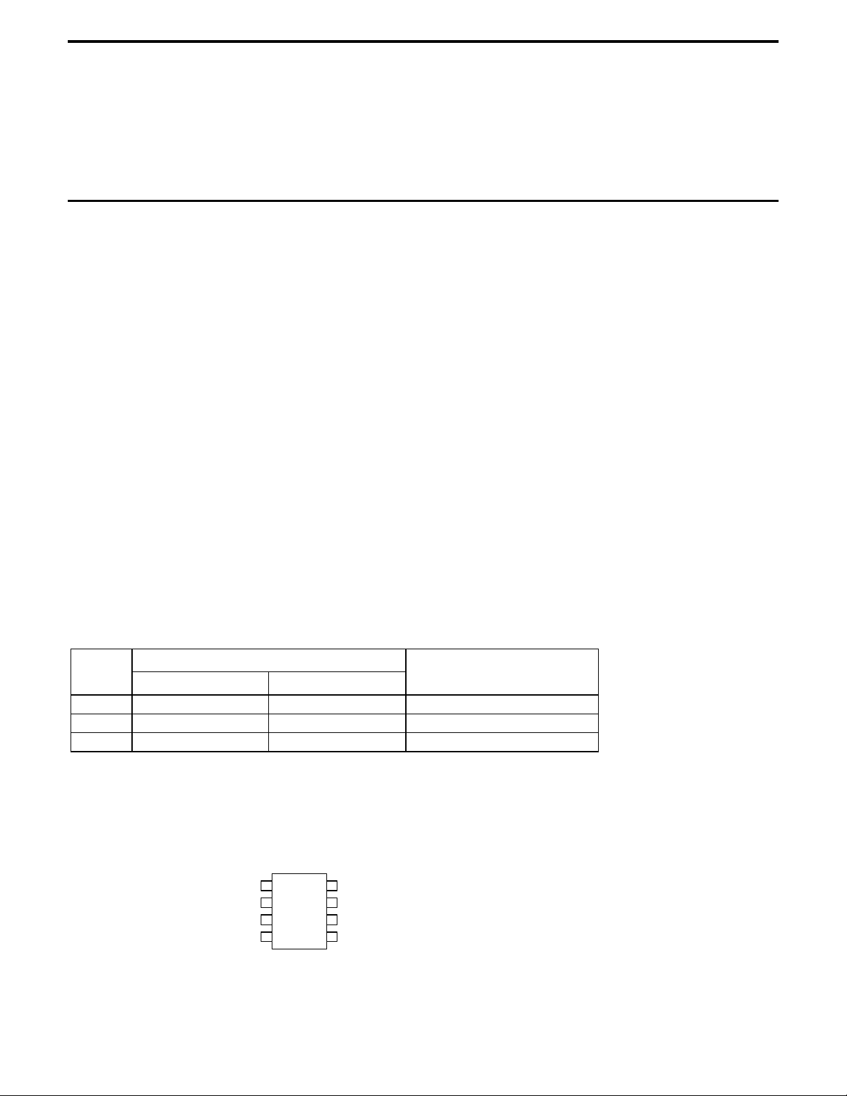
PIN CONNECTIONS
8 Lead SOIC/ 8Lead PDIP
VOS TRIM
+IN
-IN
1
2
3
4
V-
8
VOS TRIM
7
V+
6 OUT
5
N/C
Top View
Advanced Monolithic Systems, Inc. 6680B Sierra Lane, Dublin, CA 94568 Phone (925) 556-9090 Fax (925) 556-9140
Page 2
AMSOP-77
ABSOLUTE MAXIMUM RATINGS (Note1)
Supply Voltage
Differential Input Voltage
Input Voltage
±22V
±30V
±22V
Output Short Circuit Duration Indefinite Thermal Resistance
Operating Temperature Range
0°C to70°C
Storage temperature
Junction Temperature
Soldering information (60 sec)
8 L SOIC
8 L PDIP
-65°C to +125°C
+150°C
300°C
158°C/W
103°C/W
ELECTRICAL CHARACTERISTICS
Electrical Characteristics at VIN =±15V and TA = +25°C unless otherwise specified.
Parameter Conditions AMSOP-77E AMSOP-77F AMSOP-77G Units
Min Typ Max Min Typ Max Min Typ Max
Input Offset Voltage 10 25 20 60 50 100
Long Term V
Stability
Input Offset Current 0.3 1.5 0.3 2.8 0.3 2.8 nA
Input Bias Current -0.2 1.2 2.0 -0.2 1.2 2.8 -0.2 1.2 2.8 nA
Input Noise Voltage
Input Noise Voltage
Density
Input Noise Current 0.1Hz to 10Hz 14 30 15 35 15 35 pA
Input Noise Current
Density
Input Resistance
Differential-Mode
Input Resistance
Common-Mode
Input Voltage Range
OS
(Note 2) 0.3 0.4 0.4
0.1Hz to 10Hz 0.35 0.6 0.38 0.65 0.38 0.65
fO = 10Hz
fO = 100Hz (Note 3)
fO = 1000Hz
fO = 10Hz
fO = 100Hz (Note 3)
fO = 1000Hz
(Note 4) 26 45 18.5 45 18.5 45
± 13 ± 14 ± 13 ± 14 ± 13 ± 14
10.3
10.0
9.6
0.32
0.14
0.12
200 200 200
18.0
13.0
11.0
0.80
0.23
0.17
10.5
10.2
9.8
0.35
0.15
0.13
20.0
13.5
11.5
0.90
0.27
0.18
10.5
10.3
9.8
0.35
0.15
0.13
20.0
13.5
11.5
0.90
0.27
0.18
µV
µV/Mo
µV
nV/√Hz
pA/√Hz
MΩ
GΩ
V
P-P
P-P
Common-Mode
Rejection Ratio
Power Supply
Rejection Ratio
Large-Signal
Voltage Gain
Output Voltage
Swing
Slew Rate
Closed-Loop
Bandwidth
Open-Loop Output
Resistance
Power Consumption
Offset Adjustment
Range
VCM = ± 13
VS = ± 13 to ± 18
RL≥2kΩ, VO =± 10V
RL ≥10kΩ
RL ≥2kΩ
RL ≥1kΩ
RL ≥2kΩ (Note 3)
A
=+1
VCL
(Note 3)
VO = 0, IO= 0 60 60 60
VS =± 15V, No Load
VS =± 3V, No Load
RP =20kΩ ± 3 ± 3 ± 3
5000 12000 2000 6000 2000 6000 V/mV
± 13.5
± 12.5
± 12.0
0.1 0.3 0.1 0.3 0.1 0.3
0.4 0.6 0.4 0.6 0.4 0.6 MHz
0.1 1.0 0.1 1.6 0.1 1.6
0.7 3.0 0.7 3.0 0.7 3.0
± 14.0
± 13.0
± 12.5
50
3.5
60
4.5
± 13.5
± 12.5
± 12.0
± 14.0
± 13.0
± 12.5
50
3.5
60
4.5
± 13.5
± 12.5
± 12.0
± 14.0
± 13.0
± 12.5
50
3.5
60
4.5
Advanced Monolithic Systems, Inc. 6680B Sierra Lane, Dublin, CA 94568 Phone (925) 556-9090 Fax (925) 556-9140
µV/V
µV/V
V
V/µs
Ω
mW
mV
Page 3
AMSOP-77
INVERTING INPUT BIAS
ELECTRICAL CHARACTERISTICS
Electrical Characteristics at VIN= ±15, 0°C ≤ TA ≤ +70°C unless otherwise specified.
Parameter Conditions AMSOP-77E AMSOP-77F AMSOP-77G Units
Min Typ Max Min Typ Max Min Typ Max
Input Offset Voltage 10 55 20 100 80 150
Average Input Offset
Voltage Drift
Input Offset Current 0.5 2.2 0.5 4.5 0.5 4.5 nA
Average Input Offset
Current Drift
Input Bias Current -0.2 2.4 4.0 -0.2 2.4 6.0 -0.2 2.4 6.0 nA
Average Input Bias
Current Drift
Input Voltage Range
Common-Mode
Rejection Ratio
Power Supply
Rejection Ratio
Large-Signal
Voltage Gain
(Note 3) 0.3 0.6 0.4 1.0 0.7 1.2
(Note 5) 1.5 40 1.5 85 1.5 85
(Note 5) 8 40 15 60 15 60
± 13.0 ± 13.5 ± 13.0 ± 13.5 ± 13.0 ± 13.5
VCM = ± 13
VS = ± 13 to ± 18
RL≥2kΩ, VO =± 10V
2000 6000 1000 4000 1000 4000 V/mV
0.1 1.0 0.1 3.0 0.1 3.0
1.0 3.0 1.0 5.0 1.0 5.0
µV
µV/°C
pA/°C
pA/°C
V
µV/V
µV/V
Output Voltage
Swing
Power Consumption
RL ≥2kΩ ± 12.0 ± 13.0 ± 12.0 ± 13.0 ± 12.0 ± 13.0
VS = ± 15V, No Load
60 75 60 75 60 75 mW
Note 1: Absolute Maximum Ratings indicate limits beyond which damage to the device may occur. Operating Ratings indicate conditions for which the device is
intended to be functional, but do not guarantee specific performance limits. For guaranteed specifications and test conditions, see the Electrical Characteristics. The
guaranteed specifications apply only for the test conditions listed.
Note 2: Long-Term Input Offset Voltage Stability refers to the averaged trend line of VOS vs. Time over extended periods after the first 30 days of operation.
Excluding the initial hour of operation, changes in V
during the first 30 operating days are typically 2.5µV. Parameter is sample tested.
OS
Note 3: Sample tested
Note 4: Guaranteed by design.
Note 5: Guaranteed by end-point limits.
TYPICAL PERFORMANCE CHARACTERISTICS
Open-Loop Gain vs Temperature
25
VS = ±15V
20
15
10
5
OPEN-LOOP GAIN (V/µV)
0
-40
0 40
TEMPERATURE (° C)
Warm-UpDrift
4
3
2
1
0
-1
-2
OFFSET VOLTAGE (µV)
-3
ABSOLUTE CHANGE IN INPUT
-4
0.5
85
TIME AFTER POWER SUPPLY TURN-ON (minutes)
0 2.5
1.5 2
1 3
TA = 25° C
VS = ±15V
NONINVERTING INPUT BIAS
3.5
Input Bias Current vs
Differrential Input Voltage
30
AT | V
| ≤ 1.0V, | IB | ≤ 7nA (OP-07C)
DIFF
20
10
0
CURRENT (mA)
-10
-20
-30
-30 -20 -10 0 10 20 30
DIFFERENTIAL INPUT VALUE (V)
VS = ±15V
TA = 25° C
V
-30
-20
-10
0
10
20
30
Advanced Monolithic Systems, Inc. 6680B Sierra Lane, Dublin, CA 94568 Phone (925) 556-9090 Fax (925) 556-9140
Page 4

TYPICAL PERFORMANCE CHARACTERISTICS (Continued)
AMSOP-77
Input Bias Current vs Temperature
4
VS = ±15V VS = ±15V
3
2
1
INPUT BIAS CURRENT (nA)
0
-50 0 50 100
TEMPERATURE (° C)
Open-Loop Frequency Response
120
80
40
0
OPEN-LOOP GAIN (dB)
-40
0 1 10 100 1k 10k 100k 1M 10M
FREQUENCY (Hz)
VS = ±15V
TA = 25° C
Input Offset Current vs Temperature
2.0
1.5
1.0
0.5
INPUT OFFSET CURRENT (nA)
-50 0 50 100
TEMPERATURE (° C)
Maximum Output Swing vs
Frequency
32
28
VS = ±15V
TA = 25° C
24
20
16
12
8
4
PEAK-TO-PEAK AMPLITUEDE (V)
0
1k 10k
100k
FREQUENCY (Hz)
1M
Open-Loop Gain vs Power
Supply Voltage
16
TA = 25° C
RL = 2kΩ
12
8
4
OPEN-LOOP GAIN (V/µV)
00
0 ±10 ±15
±5
POWER SUPPLY VOLTAGE (V)
Maximum Output Voltage vs
Load Resistance
20
VS = ±15V
TA = 25° C
15
10
VIN = ±10mV
POSITIVE SWING
NEGATIVE SWING
5
MAXIMUM OUTPUT VOLTAGE (V)
0
100 1k 10k
LOAD RESISTANCE TO GROUND (Ω)
±20
Output Short-Circuit Current vs
Time
40
VS = ±15V
TA = 25° C
35
30
25
CURRENT (mA)
+I
SC
- I
SC
20
OUTPUT SHORT-CIRCUIT
15
0 1 2 3 4
TIME FROM OUTPUT BEING SHORTED (minutes)
ABSOLUTE VALUE OF OFFSET
Untrimmed Offset Voltage vs
Temperature
85
VS = ±15V
75
RS = 100Ω
50
VOLTAGE (µV)
25
0
-50
TEMPERATURE (° C)
OP-77E
0 50
OP-77G
OP-77F
100
Advanced Monolithic Systems, Inc. 6680B Sierra Lane, Dublin, CA 94568 Phone (925) 556-9090 Fax (925) 556-9140
Page 5

TYPICAL APPLICATIONS
Precision High-Gain Differential Amplifier
+15V
R1
1kΩ
R3
1kΩ
R4
1MΩ
2
3
OP-77E
+
7
4
-15V
0.1µF
0.1µF
AMSOP-77
R2
1MΩ
The high gain, gain linearity, CMRR, low TCVOS of the OP-77 make
it possible to obtain performance not previously available in single
6
stage very high-gain amplifier applications.
For the best CMR,
1R
R2
R3
equalmust
. In this example, with a
R4
10mV differential signal, the maximum errors are as listed.
TYPE AMOUNT
COMMON-MODE VOLTAGE 0.01%/V
GAIN LINEARITY, WORST CASE 0.02%
TCV
TCI
OS
OS
0.008%/°C
0.008%/°C
Basic Current Source 100mA current Source
Bilateral Current Source
R3
1kΩ
V
IN
R1
100kΩ
R2
100kΩ
2
OP-77
3
+
R4
990Ω
6
R5
10Ω
I
≤ 15mA
OUT
V
These current sources will supply both positive and negative current into a grounded load.
R4
1
R5
+
Note that
R2
ZO
= and that for ZO to be indefinite,
R2
R3
R4R5
+
−
R1
R4R5=+
R2
R3
must
.
R1
R3
+15V
IN
R1
R2
2
OP-77
3
+
R4
50Ω
6
2N2222
2N2907
R5
-15V
GIVEN R3= R4+R5, R1=R2
I
OUT
R3
V I INOUT =
R5*R1
≤ 100mA
Advanced Monolithic Systems, Inc. 6680B Sierra Lane, Dublin, CA 94568 Phone (925) 556-9090 Fax (925) 556-9140
Page 6

TYPICAL APPLICATIONS (Continued)
AMSOP-77
Positive Current Sink Positive current Source
Precision Current Sinks
V+
R
L
I
V
IN
+
OP-77
-
200Ω
O
IRF520
R1
1Ω
V
IN
I
O =
R1
0V VIN ≥
FULL SCALE OF 1V,
IO = 1A/V
These simple high current sinks require that the load float between the power
supply and the sink. In these circuits, OP-77’s high gain, high CMRR, and low
TCVOS assure high accuracy.
Precision Absolute Value Amplifier
1kΩ
+15V
2
3
OP-77E
+
-15V
0.1µF
7
6
4
0.1µF
C1
30pFD11N4148
2N4393
D2
R3
2kΩ
The high gain and low TCVOS assure accurate operation with inputs from microvolts
to volts. In this circuit, this signal always appears as a common-mode signal to the op
amps. The OP-77E CMRR of 1µV/V assures errors of less than 2ppm.
2
3
V
IN
OP-77E
+
+15V
-15V
R1
+
OP-77
-
1kΩ
0.1µF
7
6
4
0.1µF
200Ω
V
0< V
IRF520
I
O
R
L
V-
OUT
<10V
OUT
V
IN
I
O =
R1
0V VIN ≤
Low Noise Precision Reference
+15V
+
10µF
REF-01
2
6
V
O
4
REF-01
2
6
V
O
4
REF-01
2
6
V
O
4
100kΩ
100kΩ
100kΩ
0.1µF
OP-77
+
V
OUT
This circuit relies upon OP-77’s low TCVOS and noise combined with very high CMRR,
to provide precision buffering of the averaged REF-01 voltage outputs.
Advanced Monolithic Systems, Inc. 6680B Sierra Lane, Dublin, CA 94568 Phone (925) 556-9090 Fax (925) 556-9140
Page 7

PACKAGE DIMENSIONS inches (millimeters) unless otherwise noted.
8 LEAD SOIC PLASTIC PACKAGE (S)
0.189-0.197*
(4.801-5.004)
8 7 6 5
AMSOP-77
0.050
(1.270)
TYP
0.150-0.157**
(3.810-3.988)
0.004-0.010
(0.101-0.254)
0.228-0.244
(5.791-6.197)
1 2 3 4
0.053-0.069
(1.346-1.752)
0.014-0.019
(0.355-0.483)
*DIMENSION DOES NOT INCLUDE MOLD FLASH. MOLD FLASH
SHALL NOT EXCEED 0.006" (0.152mm) PER SIDE
**DIMENSION DOES NOT INCLUDE INTERLEAD FLASH. INTERLEAD
FLASH SHALL NOT EXCEED 0.010" (0.254mm) PER SIDE
8 LEAD PLASTIC DIP PACKAGE (P)
0.400*
(10.160)
MAX
8 7 6 5
0.008-0.010
(0.203-0.254)
0.010-0.020
(0.254-0.508)
0.016-0.050
(0.406-1.270)
x 45°
0°-8° TYP
S (SO-8 ) AMS DRW# 042293
0.255±0.015*
(6.477±0.381)
1 2 3 4
0.045-0.065
(1.143-1.651)
0.065
(1.651)
TYP
0.005
(0.127)
MIN
0.100±0.010
(2.540±0.254)
*DIMENSIONS DO NOT INCLUDE MOLD FLASH OR PROTUSIONS.
MOLD FLASH OR PROTUSIONS SHALL NOT EXCEED 0.010" (0.254mm)
0.130±0.005
(3.302±0.127)
(3.175)
0.018±0.003
(0.457±0.076)
0.125
MIN
0.015
(0.380)
MIN
0.300-0.325
(7.620-8.255)
0.009-0.015
(0.229-0.381)
+0.025
0.325
-0.015
+0.635
(8.255 )
-0.381
P (8L PDIP ) AMS DRW# 042294
Advanced Monolithic Systems, Inc. 6680B Sierra Lane, Dublin, CA 94568 Phone (925) 556-9090 Fax (925) 556-9140
 Loading...