

Page 1
Advanced AMS682
Monolithic INVERTING VOLTAGE DOUBLER
Systems
FEATURES APPLICATIONS
•• 99.9% Voltage Conversion Efficiency •• Portable Handheld Instrumentation
•• 92% Power Conversion Efficiency •• Cellular Phones
•• Wide Input Voltage Range +2.4V to 5.5V •• Panel Meters
•• 185µµA Supply Current •• -10V from +5V logic Supply
•• Available in SO-8 and PDIP Packages •• -6V from a Single 3V Lithium Cell
•• Only 3 external Capacitors Required •• LCD Display Bias Generator
•• Operational Amplifiers Power Supplies
GENERAL DESCRIPTION
The AMS682 is a CMOS charge pump converter that provides an inverted doubled output from a single positive supply.
Requiring only three external capacitors for full circuit implementation the device has an on -board 12kHz (typical) oscillator
which provides the clock.
Low output source impedance (typically 140Ω), provides output current up to 10mA. The AMS682 features low quiescent
current and high efficiency, making it the ideal choice for a wide variety of applications that require a negative voltage
derived from a single positive supply. The compact size and minimum external parts count of the AMS682 makes it useful in
many medium current, dual voltage analog power supplies.
The AMS682E is operational in the full industrial temperature range of -40°C to 85°C while AMS682C is operating over a
0°C to 70°C temperature range. The AMS682E/AMS682C are available in surface mount 8-Pin SOIC (SO-8) and 8-Pin
Plastic DIP (PDIP) packages.
ORDERING INFORMATION:
PACKAGE TYPE OPERATING
8 LEAD SOIC 8 LEAD PDIP
AMS682ES AMS682EP
AMS682CS AMS682CP
TEMPERATURE RANGE
-40 to 85° C
0 to 70° C
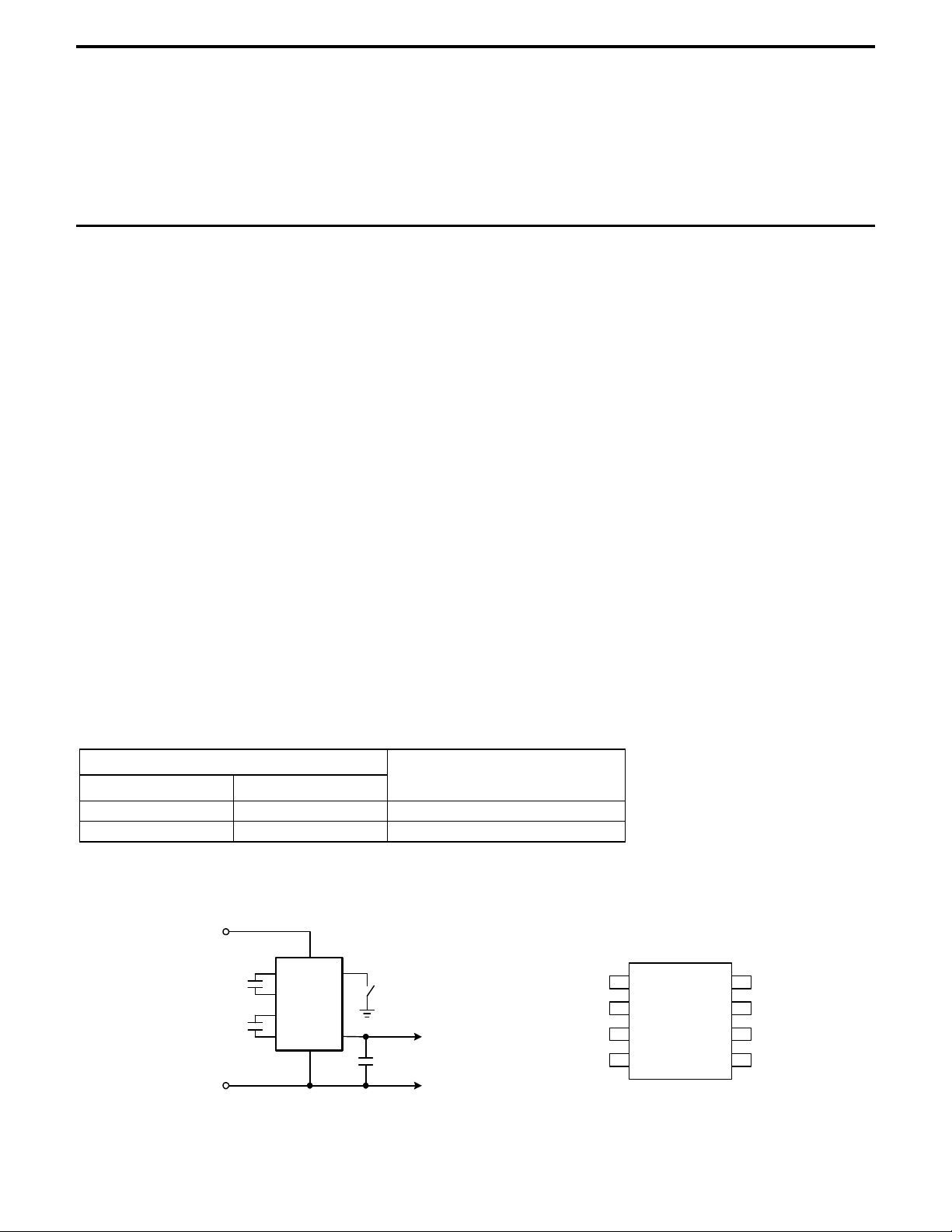
TYPICAL OPERATING CIRCUIT PIN CONFIGURATIONS
+2.4V < V
V
IN
C
1
C
2
GND
All Caps = 3.3µF
< +5.5V
IN
V
IN
+
C
+
-
+
-
ON/OFF
1
-
C
1
+
C
2
-
V
OUT
C
2
GND
C
+
V
OUT
OUT
= -(2 X VIN)
V
OUT
8-LEAD DIP/ 8-LEAD SOIC
-
C
1
2
+
2
C
2
-
C
2
V
OUT
3
4
AMS682
8
7
C
6
5
ON/OFF
+
1
V
IN
GND
Advanced Monolithic Systems, Inc. 6680B Sierra Lane, Dublin, CA 94568 Phone (925) 556-9090 Fax (925) 556-9140
Page 2
AMS682
2
+
ABSOLUTE MAXIMUM RATINGS
V
IN
VIN ∆V/∆T 1V/µsec
V
OUT
V
Short Circuit Duration Continuous Storage temperature
OUT
Power Dissipation (TA 70°C)
Plastic DIP 730mW Lead Temperature (Soldering 10sec)
SOIC 470mW
+5.8V Operating Temperature Range
AMS682E
-11.6V AMS682C
Soldering information
-40°C to 85°C
0°C to 70°C
-85°C to +150°C
+300°C
ELECTRICAL CHARACTERISTICS
Electrical Characteristics at VIN =+5V and TA = +25°C test circuit figure 1, unless otherwise specified.
Parameter
Supply Voltage Range
Supply Current
V
IN
I
IN
Conditions
RL=2kΩ
RL = ∞
RL = ∞
V
Source Resistance
OUT
Source Resistance
Oscillator Frequency F
Power Efficiency P
Voltage Conversion Efficiency V
R
OUT
OSC
EFF
OUTEFF
I
I
-
I
= 5mA , V
L
RL = 2kΩ
V
L =
-
=10mA
L
OUT RL
10mA
IN
= ∞
= 2.8V
PIN DESCRIPTION
PIN NO
8-PIN DIP/SOIC SYMBOL DESCRIPTION
1 C
2 C
3 C
4 V
5 GND Input. Device ground.
6 V
7 C
8 ON/OFF ON/OFF Oscilator.
-
1
-
2
OUT
IN
+
1
Input. Capacitor C1 negative
terminal.
Input. Capacitor C2 positive
terminal.
Input. Capacitor C2 negative
terminal
Output. Negative output voltage
(-2VIN)
Input. Power supply voltage.
Input. Capacitor C1 positive
terminal.
AMS682
Min Typ Max
2.4
90 92
99 99.9
185
140
170
12
Units
5.5 V
300
400
180
230
320
V
IN
(+5V)
GND
6
V
7 8
IN
+
C
ON/OFF
+
1
C
1
1
-
-
C
1
2
+
C
+
2
C
2
3
V-
-
-
OUT
C
2
GND
5
All Caps = 3.3µF
-
4
C
OUT
+
V
OUT
R
L
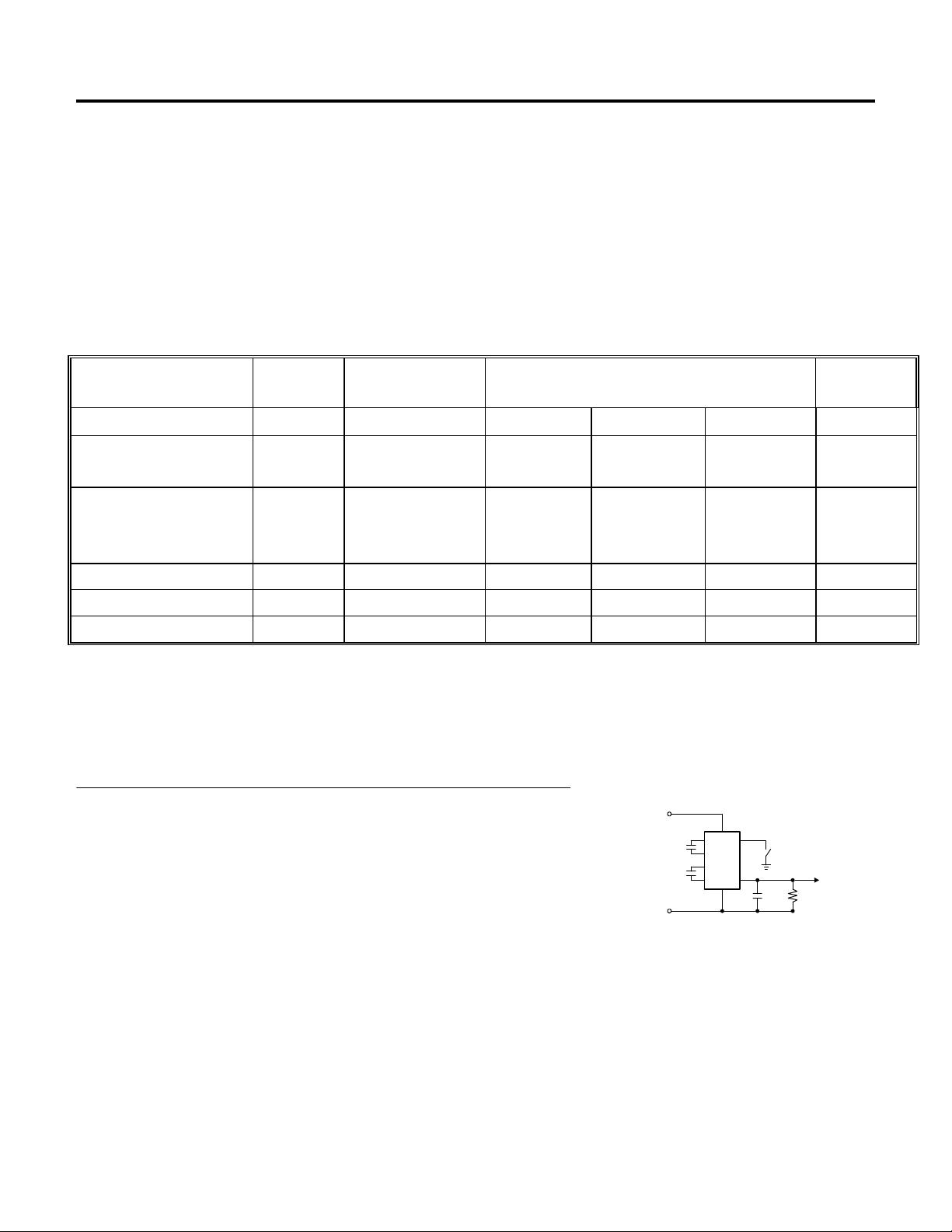
Figure 1. AMS682 Test Circuit
µA
Ω
kHz
%
%
Advanced Monolithic Systems, Inc. 6680B Sierra Lane, Dublin, CA 94568 Phone (925) 556-9090 Fax (925) 556-9140
Page 3
AMS682
1
+
2
+
2
3
OUT
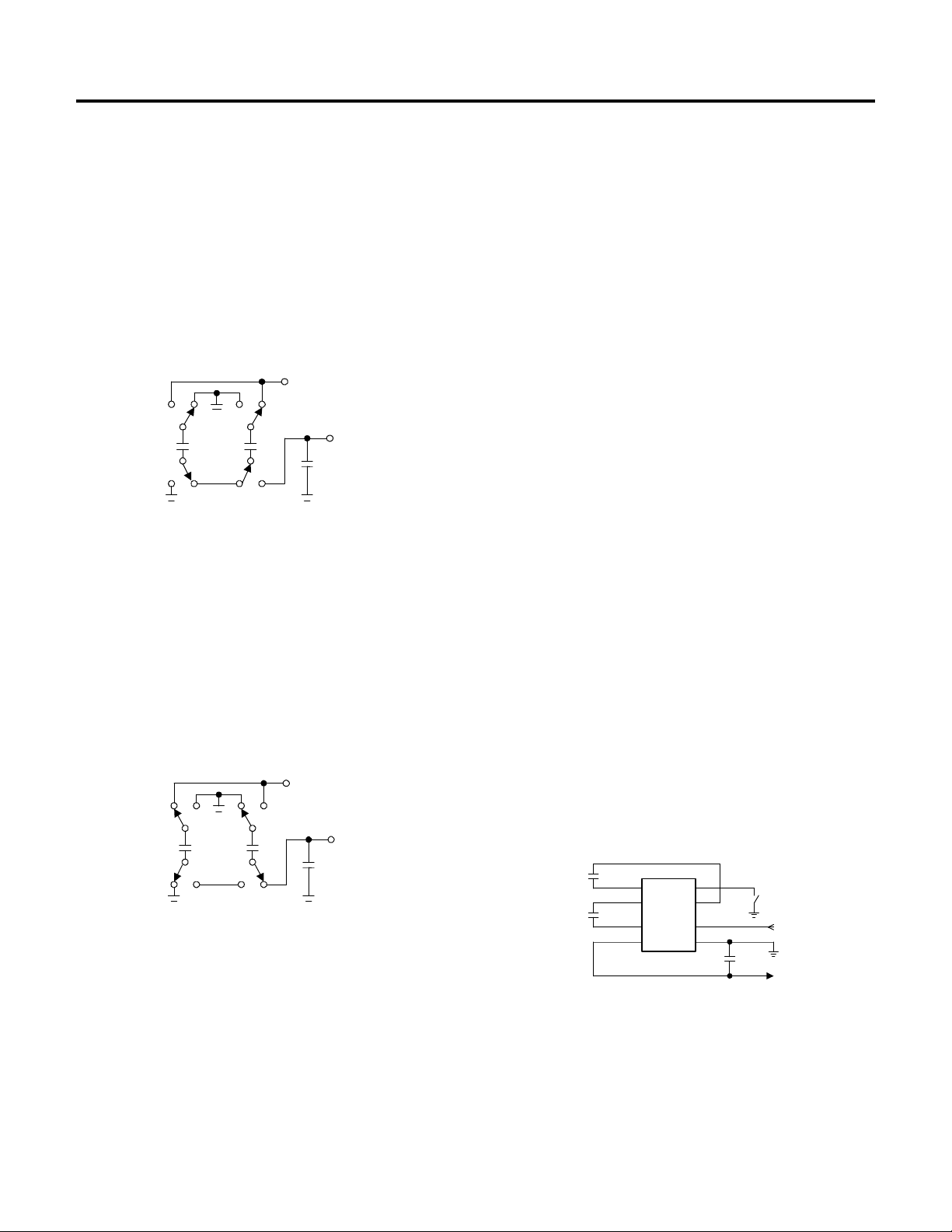
DETAILED DESCRIPTION
Phase 1
VSS charge storage- before this phase of the clock cycle,
capacitor C1 is already charged to +5V. C
to ground and the charge in C
Since C
is at +5V, the voltage potential across capacitor C
-
is transferred to C
1
is now -10V.
VIN =+5V
SW1
+
C1 C2
-
+
SW2
SW3
SW4
-5V
Figure 2. Charge Pump - Phase 1
Phase 2
is then switched
-
.
2
V
OUT
C
3
+
EFFICIENCY CONSIDERATIONS
Theoretically a charge pump voltage multiplier can approach
100% efficiency under the following conditions:
• The charge pump switches have virtually no offset and are
extremely low on resistance.
• Minimal power is consumed by the drive circuitry.
• The Impedances of the reservoir and pump capacitors are
negligible.
For the AMS682, efficiency is as shown below:
Voltage Efficiency = V
V
V
Power Loss = I
There will be a substantial voltage difference between V
2VIN if the impedances of the pump capacitors C1 and C2 are
high with respect to their respective output loads.
If the values of the reservoir capacitor C3 are larger the output
ripple will be reduced. The efficiency will be improved if both
pump and reservoir capacitors have larger values. ( See
“Capacitor Selection” in Application Section.)
/ (-2VIN )
OUT
= -2VIN + V
OUT
DROP
(V
OUT
= (I
DROP
OUT
)
) (R
DROP
OUT
)
and
OUT
VSS transfer- phase two of the clock connects the negative
terminal of C2 to the negative side of reservoir capacitor C
and the positive terminal of C2 to the ground, transferring the
generated -10V to C3. Simultaneously, the positive side of
capacitor C1 is switched to +5V and the negative side is
connected to ground. C2 is then switched to VCC and GND and
Phase 1 begins again.
VIN =+5V
SW1
+
C1 C2
-
+
SW2
SW4
-10V
SW3
V
C
+
OUT
3
Figure 3. Charge Pump - Phase 2
MAXIMUM OPERATING LIMITS
The AMS682 has on-chip zener diodes that clamp VIN to
approximately 5.8V, and V
maximum supply voltage will potentially damage the chip.
With an input voltage of 2V to 5.5V the AMS682 will operate
over the entire operating temperature range.
to -11.6V. Exceeding the
APPLICATIONS
Negative Doubling Converter
The AMS682 is most commonly used as a charge pump voltage
converter which provides a negative output of two times a
positive input voltage (Fig.4)
+
22µF
C
1
+
C
2
22µF
1
C
C
3
C
4
V-
-
1
+
2
-
2
OUT
ON/OFF
V
GND
8
72
+
C
1
C
3
22µF
V
GND
V
IN
-
6
IN
5
+
Figure 4. Inverting Voltage Doubler
OUT
Advanced Monolithic Systems, Inc. 6680B Sierra Lane, Dublin, CA 94568 Phone (925) 556-9090 Fax (925) 556-9140
Page 4

APPLICATIONS (Continued)
OUT
OUT
OUT
PUMP
OUT
OUT
AMS682
Capacitor Selection
The output resistance of the AMS682 is determined in part by
the ESR of the capacitors used. An expression for R
is
derived as shown below:
R
= 2( R
OUT
+2(R
+1/ (f
SW1+RSW2
SW1+RSW2
PUMP
+ESRC1+ R
+ESRC1+ R
X C1) +1/ (f
SW3+RSW4
SW3+RSW4
X C2) + ESR
PUMP
+ESRC2)
+ESRC2)
C3
Assuming all switch resistances are approximately equal:
R
= 16 RSW+ 4ESRC1+ 4ESRC2+ ESR
OUT
+1/ (f
R
is typically 140Ω at +25°C with VIN =+5V and 3.3µF
X C1) +1/ (f
PUMP
PUMP
C3
X C2)
low ESR capacitors. The fixed term (16RSW) is about 8090Ω. Increasing or decreasing values of C1 and C2 will affect
efficiency by changing R
Table 1 shows R
.
OUT
for various values of C1 and C2 (assume
0.5Ω ESR). C1 must be rated at 6VDC or greater while C2
and C3 must be rated at 12VDC or greater.
Output voltage ripple is affected by C3. Typically the larger
the value of C3 the less the ripple for a given load current.
The formula for p-p V
RIPPLE
is :
Paralleling devices
Paralleling multiple AMS682 reduces the output resistance of
the converter. The effective output resistance is the output
resistance of one device divided by the number of devices.
Figure 5 illustrates how each device requires separate pump
capacitors C1 and C2, but all can share a single reservoir
capacitor.
-5V Regulated Supply From A Single 3V Battery
Figure 6 shows a -5V power supply using one 3V battery.
The AMS682 provides -6V at V
-
, which is regulated to -5V
OUT
by the negative LDO. The AMS682 input can vary from 3V to
5.5V without affecting regulation significantly. A voltage
detector is connected to the battery to detect undervoltage.
This unit is set to detect at 2.7V. With higher input voltage,
more current can be drawn from the outputs of the AMS682.
With 5V at VIN , 10mA can be drawn from the regulated
output. Assuming 150Ω source resistance for the converter,
with IL=10mA, the charge pump will drop 1.5V.
V
= [1/[2(f
RIPPLE
For a 10µF (0.5Ω ESR), f
X C3)]+2(ESRC3)] (I
PUMP
)
OUT
= 10kHz and I
=10mA the
peak -to-peak ripple voltage at the output will be less than
60mV. In most applications (I
≤ 10mA) a 10-20µF
capacitor and 1-5µF pump capacitors will be sufficient. Table
2 shows V
Table 1. R
C1, C2 (µµF) R
for different values of C3 (assume 1Ω ESR).
RIPPLE
vs. C1, C2 Table 2. V
OUT
(ΩΩ) C3(µµF)
OUT
0.05 4085 0.50 1020
0.10 2084 1.00 520
0.47 510 3.30 172
1.00 285 5.00 120
3.30 145 10.00 70
5.00 125 22.00 43
10.00 105 100.00 25
22.00 94
100.00 87
Peak-to-Peak vs. C3 (I
RIPPLE
V
RIPPLE
=10mA)
OUT
(mV)
Advanced Monolithic Systems, Inc. 6680B Sierra Lane, Dublin, CA 94568 Phone (925) 556-9090 Fax (925) 556-9140
Page 5

APPLICATIONS (Continued)
V
IN
AMS682
GND
10µF
10µF
+
+
-
VIN
C1+
-
C1C2+
C2-
GND
V
OUT
10µF
10µF
+
-
+
-
C1+
C1C2+
C2-
VIN
GND
V
OUT
C
Figure 5. Paralleling AMS682 for Lower Output Source Resistance
NEGATIVE
SUPPLY
-
-
22µF
OUT
+
VIN
C1+
C1C2+
-
C2- V
OUT
GND
- 22µF
+ C
OUT
+
- 1µF
V
SS
V
IN VOUT
NEG. LDO
VOLTAGE
DETECT.
VIN V
V
SS
OUT
GROUND
-5 SUPPLY
LOW BATTERY
10µF
+ -
3V
- 10µF
-
+
+
Figure 6. Negative Supply Derived from 3V Battery
Advanced Monolithic Systems, Inc. 6680B Sierra Lane, Dublin, CA 94568 Phone (925) 556-9090 Fax (925) 556-9140
Page 6

AMS682
TYPICAL PERFORMANCE CHARACTERISTICS (F
V
vs. Load Current
OUT
10 15
LOAD CURRENT
Output Source Resistance vs. Temperature
= 10mA
)
Ω
-7.5
VIN = 5V
-8.0
-8.5
(V)
-9.0
OUT
V
-9.5
-10.0
-10.5
0 5
200
VIN = 5V
I
OUT
180
160
140
120
= 12kHz)
OSC
240
Ω)
220
200
180
160
140
OUTPUT RESISTANCE (
120
300
250
A)
µ
200
150
1
NO LOAD
Output Resistance vs. V
2 3 4
VIN (V)
Supply Current vs. V
IN
C1-C3 = 3.3µF
5
IN
6
100
80
OUTPUT SOURCE RESISTANCE (
-50
0
TEMPERATURE (°C)
100
Output Ripple vs. Output Current
C3 = 10µF
200
150
100
50
VIN = 5V
50
OUTPUT RIPPLE (mV PK-PK)
0
0
5 10
OUTPUT CURRENT (mA)
100
SUPPLY CURRENT (
50
1 2
C3 = 100µF
15 20
3 4 6
VIN (V)
5
Advanced Monolithic Systems, Inc. 6680B Sierra Lane, Dublin, CA 94568 Phone (925) 556-9090 Fax (925) 556-9140
Page 7

PACKAGE DIMENSIONS inches (millimeters) unless otherwise noted.
8 LEAD SOIC PLASTIC PACKAGE (S)
0.189-0.197*
(4.801-5.004)
8 7 6 5
AMS682
0.050
(1.270)
TYP
0.150-0.157**
(3.810-3.988)
0.004-0.010
(0.101-0.254)
0.228-0.244
(5.791-6.197)
1 2 3 4
0.053-0.069
(1.346-1.752)
0.014-0.019
(0.355-0.483)
*DIMENSION DOES NOT INCLUDE MOLD FLASH. MOLD FLASH
SHALL NOT EXCEED 0.006" (0.152mm) PER SIDE
**DIMENSION DOES NOT INCLUDE INTERLEAD FLASH. INTERLEAD
FLASH SHALL NOT EXCEED 0.010" (0.254mm) PER SIDE
8 LEAD PLASTIC DIP PACKAGE (P)
0.400*
(10.160)
MAX
8 7 6 5
0.008-0.010
(0.203-0.254)
0.010-0.020
(0.254-0.508)
0.016-0.050
(0.406-1.270)
x 45°
0°-8° TYP
S (SO-8 ) AMS DRW# 042293
0.255±0.015*
(6.477±0.381)
1 2 3 4
0.045-0.065
(1.143-1.651)
0.065
(1.651)
TYP
0.005
(0.127)
MIN
0.100±0.010
(2.540±0.254)
*DIMENSIONS DO NOT INCLUDE MOLD FLASH OR PROTUSIONS.
MOLD FLASH OR PROTUSIONS SHALL NOT EXCEED 0.010" (0.254mm)
0.130±0.005
(3.302±0.127)
(3.175)
0.018±0.003
(0.457±0.076)
0.125
MIN
0.015
(0.380)
MIN
0.300-0.325
(7.620-8.255)
0.009-0.015
(0.229-0.381)
+0.025
0.325
-0.015
+0.635
(8.255 )
-0.381
P (8L PDIP ) AMS DRW# 042294
Advanced Monolithic Systems, Inc. 6680B Sierra Lane, Dublin, CA 94568 Phone (925) 556-9090 Fax (925) 556-9140
 Loading...