

Page 1
http://www.BDTIC.com/AMS
Advanced AMS6101
Monolithic 2A SWITCH STEP-UP DC/DC CONVERTER
Systems
RoHS compliant
FEATURES APPLICATIONS
• 2A, 0.2Ω, internal switch • LCD TVs and LCD monitors
• Operating voltage as low as 2.7V • Battery Chargers
• 600 kHz operation frequency • Portable (Notebook) Computers
• Over temperature protection • Handheld Devices
• 8-Lead SOIC-EDP package • Portable Applications
GENERAL DESCRIPTION
The AMS6101 is an adjustable step-up DC/DC converter with a 2A internal switch. With the ability to set the output voltage up
to 23V, the AMS6101 is an ideal part for biasing TFT displays. The AMS6101 can be operated at switching frequencies of 600
kHz allowing for easy filtering and low noise. An external compensation pin gives the user flexibility in setting frequency
compensation, which makes possible the use of small, low ESR ceramic capacitors at the output. The AMS6101 is available in a
low profile 8-lead SOIC EDP (thermally enhanced) package.
ORDERING INFORMATION PIN CONNECTIONS
OUTPUT PACKAGE TYPE TEMP.
VOLTAGE 8 Lead SOIC RANGE
Adjustable AMS6101S -25°C to 125°C
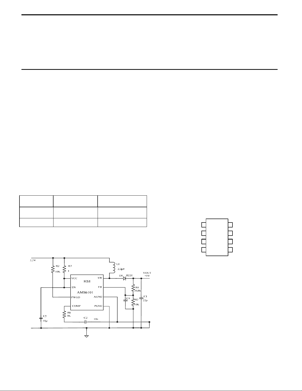
TYPICAL APPLICATION
• Consumer Electronics
• GSM/CDMA Phones
• Digital Cameras
AGND
8L SOIC
SO Package (S)
1
VCC
2
PGD
3
SW
4
Top View
8
7
6
5
EN
PGND
FB
COMP
Advanced Monolithic Systems, Inc.
Page 2

http://www.BDTIC.com/AMS
PIN DESCRIPTION
AMS6101
PIN
NUMBERS
1 VCC Analog power input.
2 PWGD Power good output. Open collector output. A low on the pin indicates that the output is less
3 SW Power switch input. Internal switch connected between SW pin and GND pin.
4 AGND Analog ground.
5 COMP Compensation network connection. Connected to the output of the voltage error amplifier.
6 F/B Feedback input pin of the error comparator.
7 PGND Power Ground-Noisy internal ground-Return currents from the power switch (SW).
8 EN Shutdown control input, active high.
NAME DESCRIPTION
AMS6101
than the desired output voltage. There is an internal rising filter on the output of the PWGD
comparator.
Advanced Monolithic Systems, Inc.
Page 3

AMS6101
http://www.BDTIC.com/AMS
ABSOLUTE MAXIMUM RATINGS (note 1)
VCC 15V Maximum Junction Temperature 150°C
SW Voltage 23V Power Dissipation (Note2) Internally Limited
F/B Voltage 7V Lead Temperature 300°C
Comp 7V Vapor Phase (60 sec) 215°C
EN 7V Infrared (15 sec) 220°C
PWGD 15V ESD Susceptibility 2kV
ELECTRICAL CHARACTERISTICS
Electrical Characteristics at TA= 25 °C, VIN=2.7V, IL = 0A (unless otherwise noted)
PARAMETER
Quiescent Current FB = 0V (Not Switching)
Feedback Voltage
Switch Current Limit
Load Regulation
Feedback Voltage Line Regulation
FB Pin Bias Current
Input Voltage Range 2.5 15 V
Error Amp Transconductance
Error Amp Voltage Gain
Maximum Duty Cycle
Switching Frequency
Shutdown Pin Current
Switch Leakage Current V SW = 18V 0.01
Switch R
VIN = 2.7V, I
DSON
Enable Threshold
On Threshold
Off Threshold
Thermal Resistance Junction to Ambient 195
Note:
1). Absolute maximum ratings are limits beyond which damage to the device may occur. Operating Ratings are conditions for
which the device is intended to be functional.
2). The maximum allowable power dissipation is a function of the maximum junction temperature, T
ambient thermal resistance, θ
and the ambient temperature, TA. The maximum allowable power dissipation at any ambient
JA,
temperature is calculated using: P
cause excessive die temperature, and the regulator will go into thermal shutdown.
3). All limits guaranteed at room temperature (standard typeface) and at temperature extremes (bold typeface).
4). Typical numbers are at 25°C and represent the most likely norm.
5). Current limit at 0% duty cycle.
TEST CONDITIONS
AMS6101
Min. Typ. Max.
(Note3) (Note4) (Note3)
Units
1.3
V EN = 0V
1.2285
VIN = 2.7 (Note 5) 3
VIN = 3.3V
6.7 mV/mA
2.0V ≤ VIN ≤ 12.0V
∆I = 5µA
40
135 V/V
78
480
V EN = VIN
0.01
V EN = 0V
5
1.26
4 A
0.013 0.1 %V
0.5
135
85 %
600
-0.5
2.0
10
1.2915
20
290
720
0.1
-1
3
Output High
Output Low
(MAX) = (T
D
= 1A 0.2
SW
0.9
0.6
0.6
1.8
1.7
– TA) θJA. Exceeding the maximum allowable power dissipation will
J (MAX)
1.92
1.82
(MAX), the junction-to-
J
0.4
0.3
2.0
1.9
mA
µA
V
nA
µmho
kHz
µA
µA
Ω
V
V
V
V
Advanced Monolithic Systems, Inc.
Page 4

http://www.BDTIC.com/AMS
TYPICAL PERFORMANCE CHARACTERISTICS
Full Load Switching Full Load Ripple (Wide Band)
AMS6101
Start Up from Enable into Full Load Start Up from Enable into Light Load
Switch Full Load Rise Time Switch Full Load Fall Time
Effic iency
90
Efficiency for 5V input and 12V Output
Advanced Monolithic Systems, Inc.
88
86
84
82
80
%
78
76
74
72
70
0.1 0.15 0.2 0.25 0.3 0.35 0.4 0.45 0.5
Load Current
Page 5

http://www.BDTIC.com/AMS
PACKAGE DIMENSIONS inches (millimeters) unless otherwise noted.
8 LEAD SOIC PLASTIC PACKAGE (S)
0.189-0.197*
(4.801-5.004)
87 65
0.123 (3.12)
0.137 (3.48)
87 65
AMS6101
0.063(1.60)
0.228-0.244
(5.791-6.197)
0.053-0.069
(1.346-1.752)
0.014-0.019
(0.355-0.483)
12 34
0.138 (3.50)
0.050(1.27)0.024(0.61)
0.105(2.67)
(0.101-0.254)
0.050
(1.270)
TYP
0.150-0.157**
(3.810-3.988)
0.004-0.010
0.213(5.41)
0.090 (2.28)
0.102 (2.59)
12 34
0.010-0.020
(0.254-0.508)
0.008-0.010
(0.203-0.254)
0.016-0.050
(0.406-1.270)
*DIMENSION DOES NOT INCLUDE MOLD FLASH. MOLD FLASH
SHALL NOT EXCEED 0.006" (0.152mm) PER SIDE
**DIMENSION DOES NOT INCLUDE INTERLEAD FLASH. INTERLEAD
FLASH SHALL NOT EXCEED 0.010" (0.254mm) PER SIDE
x 45°
0°-8 ° TYP
S (SO- 8 ) AMS DRW# 0422 93
RECOMMENDED LAYOUT PATTERN
Advanced Monolithic Systems, Inc.
 Loading...