

Page 1
Advanced AMS431L
REFERENCE
Monolithic 1.2V SHUNT REGULATOR
Systems
FEATURES APPLICATIONS
•• Trimmed 0.5% Tolerance •• Battery Powered Systems
•• Wide Operating Current Range 60µµA to 100mA •• Switching Power Supplies
•• Low Reference Input Current 0.4µµA •• Adjustable Power Supplies
•• Low Dynamic Output Impedance •• Telecommunications
•• Low Output Noise •• Error Amplifiers
•• Nominal Temperature Range to 85°°C •• Notebook/Personal Computer
•• Temperature-Compensated: 60ppm/°°C •• Monitors/ VCR/ TV
•• Pagers
GENERAL DESCRIPTION
The AMS431L is a three-terminal adjustable shunt regulator with guaranteed temperature stability over the entire range of
operation. The output voltage can be set to any value between 1.24V (V
AMS431L features 0.5% initial tolerance, low dynamic output impedance and operates over a wide current range. Due to the
sharp turn-on characteristics this device is an excellent replacement for zener diodes in many applications.
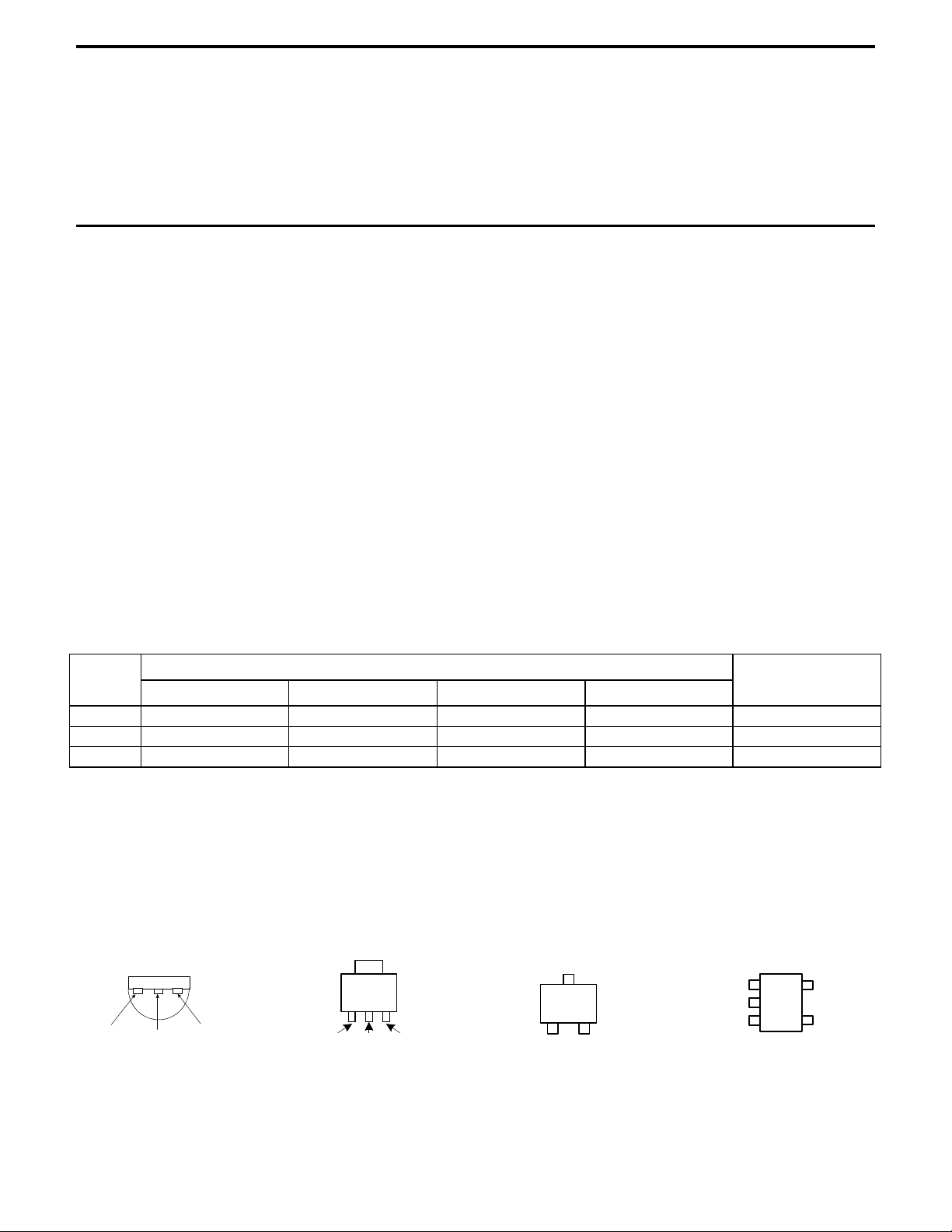
AMS431 is available in TO-92, SOT-89, 3 pin SOT-23 and 5 pin SOT-23 packages.
) and 20V by adding two external resistors. The
REF
ORDERING INFORMATION:
TOL. PACKAGE TYPE OPERATING
±0.5%
±1.0%
±2.0%
TO-92 SOT-89 3 LEAD SOT-23 5 LEAD SOT-23
AMS431LAN AMS431LAL AMS431LAM AMS431LAM1
AMS431LBN AMS431LBL AMS431LBM AMS431LBM1
AMS431LCN AMS431LCL AMS431LCM AMS431LCM1
TEMP. RANGE
-40 to +85° C
-40 to +85° C
-40 to +85° C
PIN CONNECTIONS
TO-92 SOT-89 3L SOT-23 5L SOT-23
Plastic Package (N) (L) (M) (M1)
ANODE
REF
1 2 3
ANODE
CATHODE
1 2 3
CATHODEANODEREF
CATHODEREF
N/C ANODE
N/C12
CATHODE
3
5
4
Bottom View Top View Top View Top View
Advanced Monolithic Systems, Inc. 6680B Sierra Lane, Dublin, CA 94568 Phone (925) 556-9090 Fax (925) 556-9140
Page 2
AMS431L
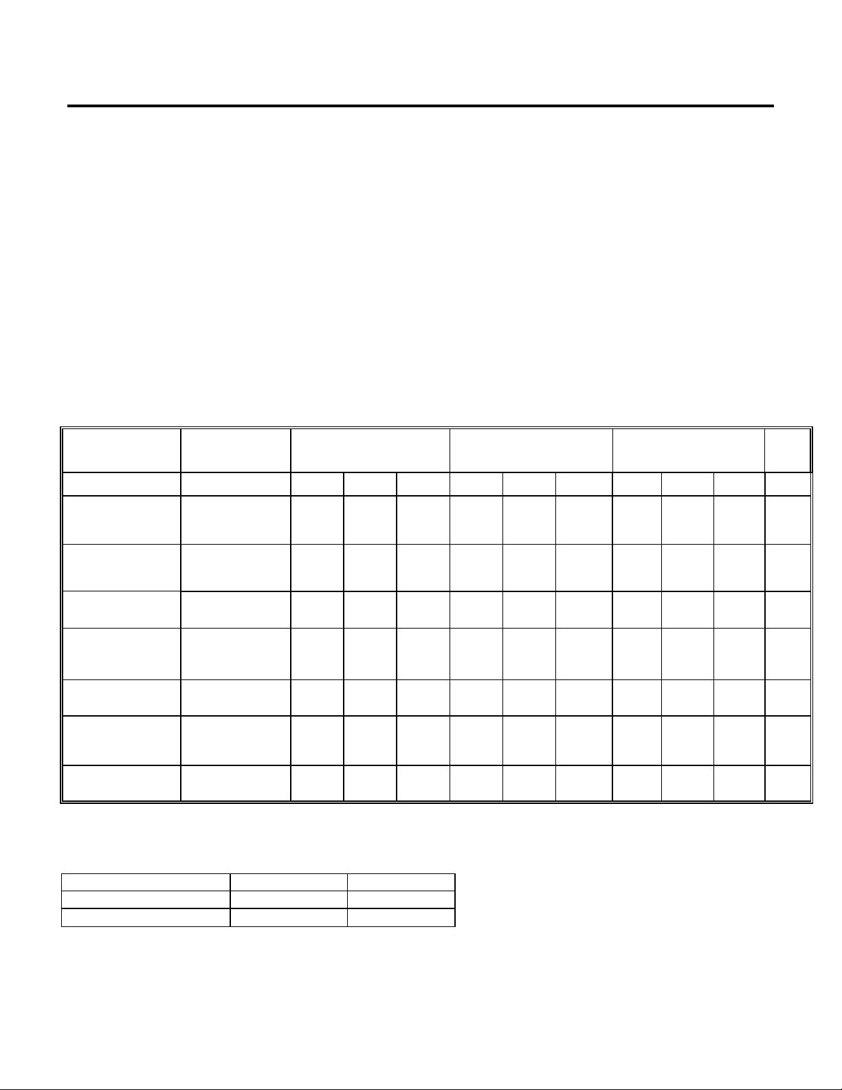
ABSOLUTE MAXIMUM RATINGS (Note 1)
Cathode Voltage (VZ) 20V Internal Power Dissipation (PD)
Continuous Cathode Current (IZ) 100mA TO-92 Package 0.78W
Reference Input Current (I
Junction Temperature (TJ)
Storage temperature
Lead Temperature (Soldering, 10sec.)
Note 1 : Absolute Maximum Ratings indicate limits beyond which damage to the device may occur. Operating Ratings indicate conditions for which the device is
intended to be functional, but do not guarantee specific performance limits. For guaranteed specifications and test conditions, see the Electrical Characteristics. The
guaranteed specifications apply only for the test conditions listed.
ELECTRICAL CHARACTERISTICS
Electrical Characteristics at IZ =10 mA and TA = +25°C unless otherwise noted.
) 3mA SOT-89 Package 0.91W
REF
-40°C to +125°C
SOT-23-3 Package 0.28W
SOT-23-5 Package 0.3 W
-65°C to +150°C Thermal Resistance (θJA)
265°C
TO-92 Package
SOT-89 Package
SOT-23-3 Package
SOT-23-5 Package
160°C/W
110°C/W
410°C/W
410°C/W
Parameter Conditions
Reference Voltage 1.234 1.240 1.246 1.228 1.240 1.252 1.215 1.240 1.265 V
Deviation of Reference
Input Voltage over
Temperature
Ratio of Change in
Reference Voltage to
Cathode Voltage
Reference Input Current
Reference Input Current
Deviation over
Temperature
Off State Cathode
Current
Dynamic Output
Impedance
Minimum Operating
Current
VZ = V
TA = -40°C to +85°C
IZ = 10mA
∆V = from V
R1 =10kΩ, R2 = ∞Ω
(test circuit 2)
R1 =10kΩ, R2 = ∞Ω
TA = Full Range
(test circuit 2)
VZ = 6V, V
( test circuit 3)
f < 1KHz, VZ = V
IZ =100µA to 100mA
(test circuit 1)
VZ = V
(test circuit 1)
REF
REF
(circuit 1)
REF
= 0V
REF
REF
AMS431LA
Min Typ Max
10 25 10 25 10 35 mV
-0.5
0.15 0.5 0.15 0.5 0.15 0.5
0.1 0.4 0.1 0.4 0.1 0.4
0.04 0.1 0.04 0.1 0.04 0.1
0.25 0.4 0.25 0.4 0.25 0.4
60 80 60 80 60 80
-2.7 -0.5 -2.7 -0.5 -2.7 mV/V
AMS431LB
Min Typ Max
AMS431LC
Min Typ Max
Units
µA
µA
µA
Ω
µA
RECOMMENDED OPERATING CONDITIONS:
Min Max
Cathode Voltage, (VZ) V
Cathode Current, (IZ)
REF
80µA
Advanced Monolithic Systems, Inc. 6680B Sierra Lane, Dublin, CA 94568 Phone (925) 556-9090 Fax (925) 556-9140
20 V
100mA
Page 3
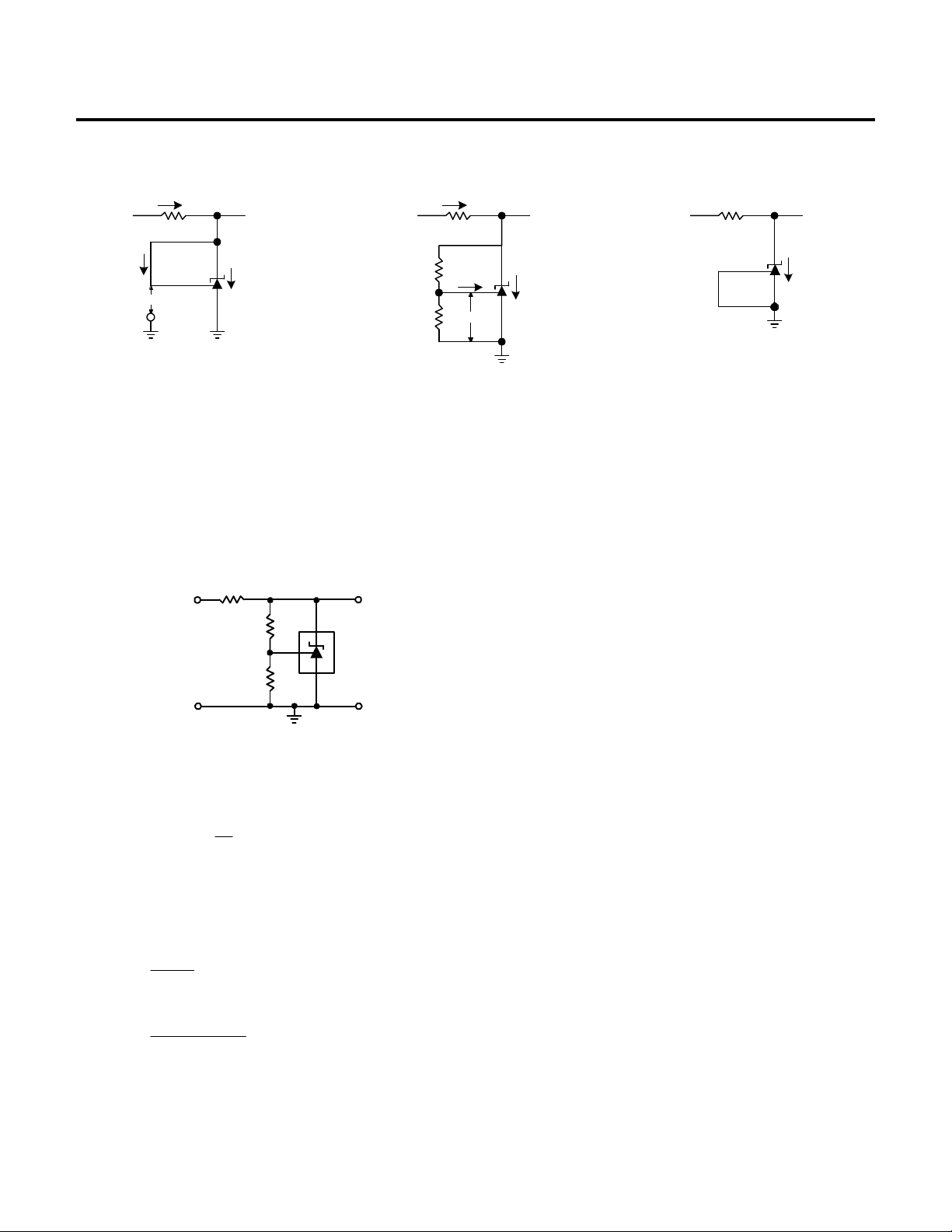
TEST CIRCUITS
AMS431L
I
VZ = V
Z
V
IN
I
REF
V
REF
Figure 1. Test Circuit for VZ=V
TYPICAL APPLICATIONS
V
IN
R1
V
REF
R2
GND
I
Z
REF
REF
V
Z
.
vs IZ.
V
IN
Figure 3. Test Circuit for Off-State Current
REF
REF
V
IN
R1
I
REF
V
R2
REF
Figure 2. Test Circuit for V
Test circuit for I
V
OUT
V
IZ OFF
Z
1) Set the V
according to the following equation:
OUT
R1
1V V REFREFOUT +
+=
R2
R1I
2) Choose the value of R as follows:
• The maximum limit for R should be such that the cathode current, IZ is greater than the minimum operating current (80µA) at V
IN(min)
.
• The minimum limit for R should b such that IZ does not exceed 100mA under all load conditions, and the instantaneous turn-on value for IZ does not exceed
150mA. Both of the following conditions must be met:
V
IN(max)
min Ion - turnousinstantanelimit to
R ≥
R Z
min
≥
( )
150mA
V-V
OUTIN(max)
( )
OUT(min)
100mAI
+
Z
conditions operating normalunder Ilimit to
Advanced Monolithic Systems, Inc. 6680B Sierra Lane, Dublin, CA 94568 Phone (925) 556-9090 Fax (925) 556-9140
Page 4

TYPICAL PERFORMANCE CHARACTERISTICS
AMS431L
Cathode Current vs. Cathode Voltage
300
TA =25° C
VR= V
200
REF
100
0
-100
-200
CATHODE CURRENT (µA)
-300
-1
-0.5
0
CATHODE VOLTAGE (V)
Reference Input Current vs.
Junction Temperature
150
IZ= 10mA
R1= 10k
Ω
R2=
125
∞
100
75
REFERENCE INPUT CURRENT (nA)
50
-50
-25 0
25 50 75 100 125
JUNCTION TEMPERATURE (° C)
0.5 1
1.5
150
Cathode Current vs. Cathode Voltage
150
TA =25° C
VR= V
100
REF
50
0
-50
-100
CATHODE CURRENT (mA)
-150
-1.5 -1 0 0.5 1
-0.5
CATHODE VOLTAGE (V)
Ratio of Delta Reference Voltage to Delta
Cathode Voltage vs. Junction Temperature
1.2
IZ= 10mA
1.1
∆
1.0
VZ= 16V to V
REF
0.9
0.8
0.7
(-mV/V)
Z
0.6
0.5
/∆V
0.4
REF
0.3
∆V
0.2
0.1
0.0
-50
-25 0
25 50 75 100 125
JUNCTION TEMPERATURE (° C)
1.5
150
Reference Voltage vs.
Junction Temperature
1.248
1.246
IZ= 100mA
1.244
1.242
1.240
1.238
1.236
REFERENCE VOLTAGE (V)
1.234
-50
-25 0
25 50 75 100 125
IR= 60µA
JUNCTION TEMPERATURE (° C)
Off State Cathode Current vs.
Junction Temperature
250
V
= 0V
REF
200
VR= 16V
150
100
50
0
-50
CATHODE CURRENT(OFF STATE) (nA)
-25 0
25 50 75 100 125
VZ= 6V
JUNCTION TEMPERATURE (° C)
150
150
Reference Impedance vs.
Reference Impedance vs. Frequency
Junction Temperature
0.50
0.45
0.40
0.35
IZ = 0.1 to 100mA
VZ= V
REF
f< 1kHz
100
TA =25° C
10
0.30
0.25
1
0.20
0.15
0.10
0.05
REFERENCE IMPEDANCE (Ω)
0
-50 25 50 75 100 125
-25 0
JUNCTION TEMPERATURE (° C)
150
REFERENCE IMPEDANCE (Ω)
0.1
0.01
10
1
100 1000 100000
FREQUENCY (kHz)
Advanced Monolithic Systems, Inc. 6680B Sierra Lane, Dublin, CA 94568 Phone (925) 556-9090 Fax (925) 556-9140
Page 5

TYPICAL PERFORMANCE CHARACTERISTICS (Continued)
AMS431L
Small Signal Gain and Phase Shift
vs. Frequency
80
70
60
50
40
30
20
10
0
SMALL SIGNAL GAIN (dB)
-10
-20
1k 10k 100k 1000k
100
FREQUENCY (Hz)
Stability Boundary Condition
3.5
TA =25° C
3.0
Stable
2.5
2.0
1.5
1.0
VZ = V
Stable
REF
-180
-225
-270
-315
-360
PHASE SHIFT (deg)
10µF
+
-
Small Signal Gain and Phase Shift
Test Circuit
I
Z
15k
8.25k
232
+
-
Stability Circuit
I
Z
R1
C
L
R2
OUT
GND
0.5
CATHODE CURRENT (mA)
0.0
0.001
0.01 0.1 1
VZ = 2V
10
LOAD CAPACITANCE (µF)
Advanced Monolithic Systems, Inc. 6680B Sierra Lane, Dublin, CA 94568 Phone (925) 556-9090 Fax (925) 556-9140
Page 6

PACKAGE DIMENSIONS inches (millimeters) unless otherwise noted.
3L TO-92 PLASTIC PACKAGE (N)
AMS431L
0.060±0.005
(1.524±0.127)
DIA
0.180±0.005
(4.572±0.127)
0.500
(12.70)
MIN
0.050±0.005
(1.270±0.127)
0.180±0.005
(4.572±0.127)
0.90
(2.286)
NOM
5° NOM
UNCONTROLLED
0.050
(1.270)
LEAD DIMENSIONS
MAX
0.015±0.002
0.016±0.003
(0.406±0.076)
(0.381±0.051)
5 LEAD SOT-23 PLASTIC PACKAGE (M1)
0.110-0.120
(2.794-3.048)
0.060±0.010
(1.524±0.254)
10°
NOM
N (TO-92 ) AMS DRW# 042391
0.140±0.010
(3.556±0.127)
0.102-0.118
(2.60-3.00)
0.059-0.070
(1.50-1.75)
0.014-0.020
(0.350-0.50)
10°
NOM
10°
NOM
0.018-0.024
(0.457-0.610)
0.0035-0.0080
(0.090-0.20)
(SOT-23-5 ) AMS DRW# 051001
0.018-0.024
(0.457-0.610)
0.036-0.051
(0.090-1.30)
0.003
(0.150)
MAX
0.037
(0.95)
TYP
0.075
(1.90)
TYP
Advanced Monolithic Systems, Inc. 6680B Sierra Lane, Dublin, CA 94568 Phone (925) 556-9090 Fax (925) 556-9140
Page 7

PACKAGE DIMENSIONS inches (millimeters) unless otherwise noted (Continued).
3 LEAD SOT-23 PLASTIC PACKAGE (M)
0.110-0.120
(2.794-3.048)
0.015-0.017
(0.381-0.432)
0.083-0.098
(2.108-2.489)
0.047-0.055
(1.194-1.397)
0.035-0.040
(0.889-1.016)
AMS431L
0.035-0.041
(0.089-1.041)
0.0005-0.0040
(0.013-0.102)
0.155-0.167
(3.94-4.25)
0.018-0.024
(0.457-0.610)
0.090-0.102
(2.29-2.60)
10°
NOM
0.070-0.080
(1.778-2.032)
SOT-89 PLASTIC PACKAGE (L)
0.173-0.181
(4.40-4.60)
0.064-0.072
(1.62-1.83)
10°
NOM
0.055-0.063
(1.40-1.60)
0.084-0.090
(2.13-2.29)
0.018-0.024
(0.457-0.610)
0.0034-0.0050
(0.086-0.127)
(SOT-23 ) AMS DRW# 051991
0.014-0.017
(0.35-0.44)
0.035-0.047
(0.89-1.20)
0.059
(1.50)
BSC
0.118
(3.00)
BSC
0.017-0.022
(0.44-0.56)
0.014-0.019
(0.36-0.48)
L (SOT-89 ) AMS DRW# 042392
Advanced Monolithic Systems, Inc. 6680B Sierra Lane, Dublin, CA 94568 Phone (925) 556-9090 Fax (925) 556-9140
 Loading...