

Page 1
www.BDTIC.com/AMS
Advanced AMS431
Monolithic PRECISION ADJUSTABLE SHUNT REGULATOR
Systems
RoHS compliant
FEATURES APPLICATIONS
•••• Trimmed 0.25% Reference •••• Battery Powered Systems
•••• Wide Operating Current Range 250µµµµA to 150mA •••• Switching Power Supplies
•••• Low Dynamic Output Impedance •••• Adjustable Power Supplies
•••• Low Output Noise •••• Linear Regulators
•••• Nominal Temperature Range -40°°°°C to 125°°°°C •••• Error Amplifiers
•••• Temperature-Compensated: 60ppm/°°°°C typ •••• Notebook/Personal Computer
•••• Internal Amplifier with 150mA Capability •••• Monitors/ VCR/ TV
GENERAL DESCRIPTION
he AMS431 is a three-terminal adjustable shunt regulator with guaranteed temperature stability over the entire range of
T
operation. The output voltage can be set to any value between 2.5V (VREF) and 36V by adding two external resistors. Due to
the sharp turn-on characteristics this device is an excellent replacement for zener diodes in many applications.
AMS431 is available in TO-92, SO-8, SOT-89 and SOT-23 packages.
ORDERING INFORMATION:
TOL. PACKAGE TYPE OPERATING
TO-92 8 LEAD SOIC SOT-89 3 LEAD SOT-23
±0.25%
±0.5%
±1.0%
AMS431AN AMS431AS AMS431AL AMS431AM
AMS431BN AMS431BS AMS431BL AMS431BM
AMS431CN AMS431CS AMS431CL AMS431CM
PIN CONNECTIONS
TO-92 8L SOIC SOT-89 3L SOT-23
Plastic Package (N) SO Package (S) (L) (M)
1 2 3
REF
ANODE
CATHODE
Bottom View
Top View Top View Top View
REF
CATHODE
ANODE
ANODE
N/C
1
2
3
4
8
7
6
5
ANODE
ANODE
N/C
•••• Pagers
1 2 3
TEMP. RANGE
-40 to +125° C
-40 to +125° C
-40 to +125° C
ANODE
CATHODEANODEREF
CATHODEREF
Advanced Monolithic Systems, Inc.
Page 2
www.BDTIC.com/AMS
AMS431
ABSOLUTE MAXIMUM RATINGS (Note 1)
Cathode Voltage (VZ) 37V Internal Power Dissipation (PD)
Continuous Cathode Current (IZ) -10mA to +150mA TO-92 Package 0.78W
Reference Input Current (I
Junction Temperature (TJ)
SOT-23 Package 0.28W
Storage temperature
Lead Temperature (Soldering, 10sec.)
SO-8 Package
SOT-89 Package
SOT-23 Package
Note 1 : Absolute Maximum Ratings indicate limits beyond which damage to the device may occur. Operating Ratings indicate conditions for which the
evice is intended to be functional, but do not guarantee specific performance limits. For guaranteed specifications and test conditions, see the Electrical
d
Characteristics. The guaranteed specifications apply only for the test conditions listed.
ELECTRICAL CHARACTERISTICS
Electrical Characteristics at IZ =10 mA and TA = +25°C unless otherwise specified.
Parameter
Conditions
) 10mA SO-8 Package 0.71W
REF
-40°C to +125°C
-65°C to +150°C
265°C
SOT-89 Package 0.91W
Thermal Resistance (ϕJA)
TO-92 Package
160°C/W
175°C/W
110°C/W
410°C/W
AMS431A
Min Typ Max
AMS431B
Min Typ Max
AMS431C
Min Typ Max
Units
Reference Voltage 2.489 2.495 2.501 2.483 2.495 2.507 2.470 2.495 2.520 V
Deviation of Reference
Input Voltage over
Temperature
Ratio of Change in
Reference Voltage to
Cathode Voltage
Reference Input
Current
Reference Input
Current Deviation over
Temperature
Off State Cathode
Current
Dynamic Output
Impedance
Minimum Operating
Current
VZ = V
TA = 25°C to
+125°C
TA = -40°C to +25°C
VZ from V
10V
VZ from V
36V
R1 =10kΩ, R2 = ∞Ω
(test circuit 2)
R1 =10kΩ, R2 = ∞Ω
TA = Full Range
(test circuit 2)
VZ = 36V, V
0V
( test circuit 3)
f < 1KHz, VZ = V
IZ =100µA to 100mA
(test circuit 1)
VZ = V
(test circuit 1)
REF
REF
REF
REF
(circuit 1)
to
to
=
REF
REF
0.5 4.0 0.5 4.0 0.5 4.0
0.4 1.2 0.4 1.2 0.4 1.2
0.04 0.5 0.04 0.5 0.04 0.5
0.25 0.5 0.25 0.5 0.25 0.5
100 250 100 250 100 250
8.0
8.0
-0.5
-1.0
15
15
-2.7 -0.5 -2.7 -0.5 -2.7 mV/V
-2.0 -1.0 -2.0 -1.0 -2.0 mV/V
8.0
10
15
20
8.0
12
15
25
mV
mV
µA
µA
µA
µA
RECOMMENDED OPERATING CONDITIONS:
M
Cathode Voltage, (VZ) V
Cathode Current, (IZ) 0.25mA 120mA
Advanced Monolithic Systems, Inc.
in Max
36 V
REF
Ω
Page 3
www.BDTIC.com/AMS
AMS431
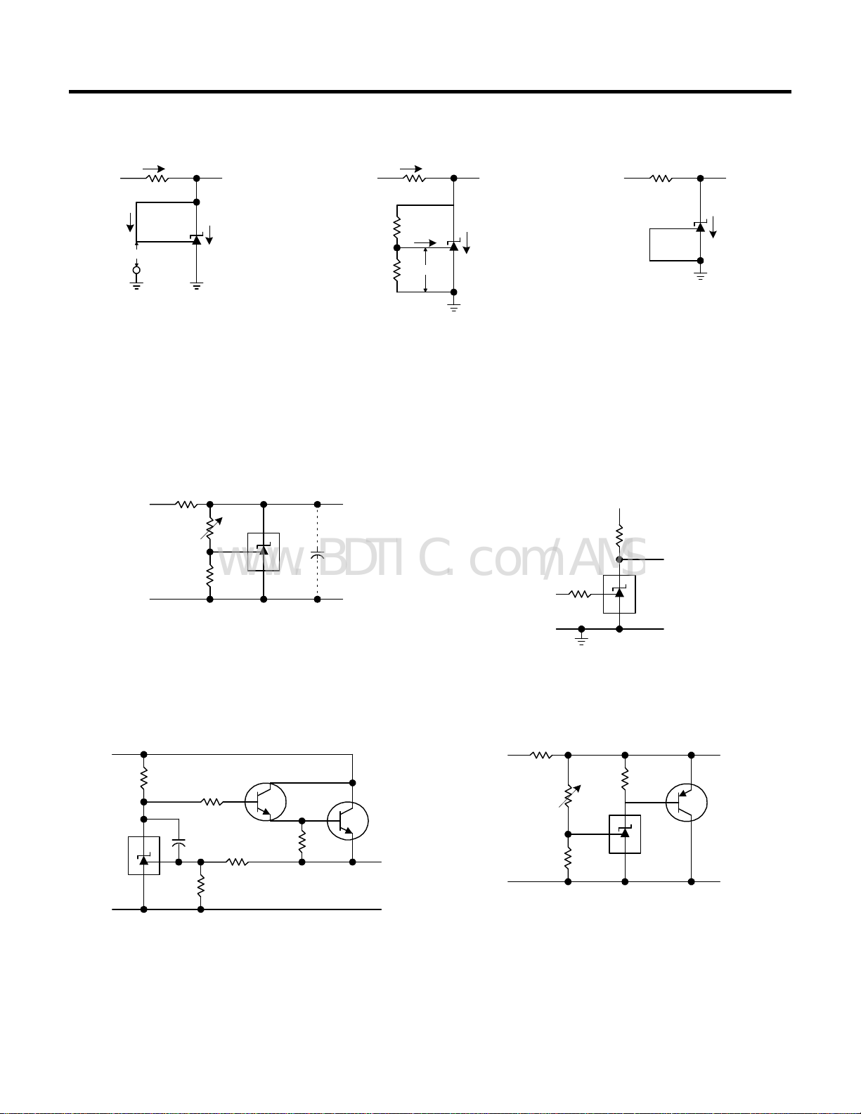
TEST CIRCUITS
I
Z
VZ = V
REF
V
IN
R1
R2
V
IN
I
REF
V
REF
Figure 1. Test Circuit for VZ=V
Figure 2. Test Circuit for V
REF
Test circuit for I
TYPICAL APPLICATIONS
Shunt Regulator
V+
V
O
V
Z
I
REF
V
REF
I
Z
V
IN
V
Z
IZ OFF
REF
REF
vs IZ.
.
Temperature Compensated Threshold
Figure 3. Test Circuit for Off-State Current
Single Supply Comparator with
V+
R1
V
REF
R2
VO ≈ (1+R1/R2)V
REF
Series Regulator
V+
30
Ω
0.01µF
R1
R2
V
O
≈ (1+R1/R2)V
V
O
REF
≈ (1+R1/R2)V
V
O
IN
V
≈
2.5V
TH
Higher Current Shunt Regulator
V+
R1
R1
REF
OUT
V
≈
2V
ON
= V+
V
OFF
GND
V
O
Advanced Monolithic Systems, Inc.
Page 4

www.BDTIC.com/AMS
AMS431
TYPICAL APPLICATIONS (Continued)
V+
R1A
Over Voltage/Under Voltage
Protection Circuit
R1B
OUT ON
WHEN
LOW < V+ < HIGH
LIMIT LIMIT
Voltage Monitor
V+
R1B
R1A
R2A
LOW LIMIT ≈ V
LOW LIMIT ≈ V
( 1+R1B/R2B)+V
REF
( 1+R1A/R2A)
REF
R2B
BE
R2A
LOW LIMIT ≈ V
LOW LIMIT ≈ V
LIMIT
( 1+R1B/R2B)+VBE LED ON WHEN
REF
( 1+R1A/R2A) LOW LIMIT < V+ < HIGH
REF
R2B
OFF
Delay Timer
V+
R
ON
C
Current Limiter or Current Source
V+
R
CL
I
O
DELAY = R*C*ln*V+/(V+)-V
REF
IO =V
REF/RCL
Constant Current Sink
V+
I
O
R
S
IO = V
REF/RS
Advanced Monolithic Systems, Inc.
Page 5

www.BDTIC.com/AMS
TYPICAL PERFORMANCE CHARACTERISTICS
500
A)
µ
400
Input Current vs V
ΤΑ = 25°
C
VZ = V
REF
Z
IZ MIN
Thermal Information
1000
SOT-89
Input Current vs V
150
ΤΑ = 25°
= V
V
Z
100
AMS431
Z
C
REF
300
200
INPUTT CURRENT (
100
0
0
1.0 2.0 3.0
CATHODE VOLTAGE (V)
500
REFERENCE VOLTAGE (V)
100
25
TO-92
SOT-23
TEMPERATURE (° C)
70 85
SO-8
125
50
INPUTT CURRENT ( mA)
0
0
1.0 2.0 3.0
CATHODE VOLTAGE (V)
PACKAGE DIMENSIONS inches (millimeters) unless otherwise noted.
3L TO-92 PLASTIC PACKAGE (N)
0.060±0.005
(1.524±0.127)
DIA
0.180±0.005
(4.572±0.127)
0.180±0.005
(4.572±0.127)
0.90
(2.286)
NOM
0.060±0.010
(1.524±0.254)
0.140±0.010
(3.556±0.127)
0.500
(12.70)
MIN
0.050±0.005
(1.270±0.127)
0.050
(1.270)
MAX
0.016±0.003
(0.406±0.076)
UNCONTROLLED
LEAD DIMENSIONS
Advanced Monolithic Systems, Inc.
5° NOM
0.015±0.002
(0.381±0.051)
10°
NOM
N (TO-92 ) AMS DRW# 042391
Page 6

www.BDTIC.com/AMS
PACKAGE DIMENSIONS inches (millimeters) unless otherwise noted (Continued).
8 LEAD SOIC PLASTIC PACKAGE (S)
0.189-0.197*
(4.801-5.004)
8 7 6 5
AMS431
0.050
(1.270)
TYP
0.150-0.157**
(3.810-3.988)
0.004-0.010
(0.101-0.254)
0.008-0.010
(0.203-0.254)
0.010-0.020
(0.254-0.508)
0.016-0.050
(0.406-1.270)
x 45°
0°-8° TYP
S (SO-8 ) AMS DRW# 042293
0.228-0.244
(5.791-6.197)
1 2 3 4
0.053-0.069
(1.346-1.752)
0.014-0.019
(0.355-0.483)
*DIMENSION DOES NOT INCLUDE MOLD FLASH. MOLD FLASH
SHALL NOT EXCEED 0.006" (0.152mm) PER SIDE
**DIMENSION DOES NOT INCLUDE INT ERLEAD FLASH. INTERLEAD
FLASH SHALL NOT EXCEED 0.010" (0.254mm) PER SIDE
SOT-89 PLASTIC PACKAGE (L)
0.173-0.181
(4.40-4.60)
0.064-0.072
(1.62-1.83)
0.055-0.063
(1.40-1.60)
0.014-0.017
(0.35-0.44)
0.155-0.167
(3.94-4.25)
0.090-0.102
(2.29-2.60)
0.059
(1.50)
BSC
0.118
(3.00)
BSC
0.017-0.022
(0.44-0.56)
0.014-0.019
(0.36-0.48)
Advanced Monolithic Systems, Inc.
0.035-0.047
(0.89-1.20)
0.084-0.090
(2.13-2.29)
L (SOT-89 ) AMS DRW# 042392
Page 7

www.BDTIC.com/AMS
PACKAGE DIMENSIONS inches (millimeters) unless otherwise noted (Continued).
3 LEAD SOT-23 PLASTIC PACKAGE (M)
0.110-0.120
(2.794-3.048)
0.015-0.017
(0.381-0.432)
0.083-0.098
(2.108-2.489)
0.047-0.055
(1.194-1.397)
0.035-0.040
(0.889-1.016)
AMS431
0.018-0.024
(0.457-0.610)
0.035-0.041
(0.089-1.041)
0.0005-0.0040
(0.013-0.102)
0.070-0.080
(1.778-2.032)
10°
NOM
10°
NOM
0.018-0.024
(0.457-0.610)
0.0034-0.0050
(0.086-0.127)
(SOT-23 ) AMS DRW# 051991
Advanced Monolithic Systems, Inc.
 Loading...