

Page 1
Low Noise, Precision
a
FEATURES
Low Offset Voltage: 50 V Max
Very Low Offset Voltage Drift: 0.3 V/ⴗC Max
Low Noise: 0.12 V p-p (0.1 Hz to 10 Hz)
Excellent Output Drive: ⴞ10 V at ⴞ50 mA
Capacitive Load Stability: to 1 F
Gain Range: 0.1 to 10,000
Excellent Linearity: 16-Bit at G = 1000
High CMR: 125 dB min (G = 1000)
Low Bias Current: 4 nA Max
May Be Configured as a Precision Op Amp
Output-Stage Thermal Shutdown
Available in Die Form
GENERAL DESCRIPTION
The AMP01 is a monolithic instrumentation amplifier designed
for high-precision data acquisition and instrumentation applications. The design combines the conventional features of an
instrumentation amplifier with a high current output stage. The
output remains stable with high capacitance loads (1 µF), a
unique ability for an instrumentation amplifier. Consequently,
the AMP01 can amplify low level signals for transmission
through long cables without requiring an output buffer. The output
stage may be configured as a voltage or current generator.
Input offset voltage is very low (20 µV), which generally elimi-
nates the external null potentiometer. Temperature changes
have minimal effect on offset; TCV
Excellent low-frequency noise performance is achieved with a
minimal compromise on input protection. Bias current is very
low, less than 10 nA over the military temperature range. High
common-mode rejection of 130 dB, 16-bit linearity at a gain of
1000, and 50 mA peak output current are achievable simultaneously. This combination takes the instrumentation amplifier
one step further towards the ideal amplifier.
AC performance complements the superb dc specifications. The
AMP01 slews at 4.5 V/µs into capacitive loads of up to 15 nF,
settles in 50 µs to 0.01% at a gain of 1000, and boasts a healthy
26 MHz gain-bandwidth product. These features make the
AMP01 ideal for high speed data acquisition systems.
Gain is set by the ratio of two external resistors over a range of
0.1 to 10,000. A very low gain temperature coefficient of
10 ppm/°C is achievable over the whole gain range. Output
voltage swing is guaranteed with three load resistances; 50 Ω,
500 Ω, and 2 kΩ. Loaded with 500 Ω, the output delivers
±13.0 V minimum. A thermal shutdown circuit prevents de-
struction of the output transistors during overload conditions.
The AMP01 can also be configured as a high performance operational amplifier. In many applications, the AMP01 can be
used in place of op amp/power-buffer combinations.
is typically 0.15 µV/°C.
IOS
Instrumentation Amplifier
AMP01*
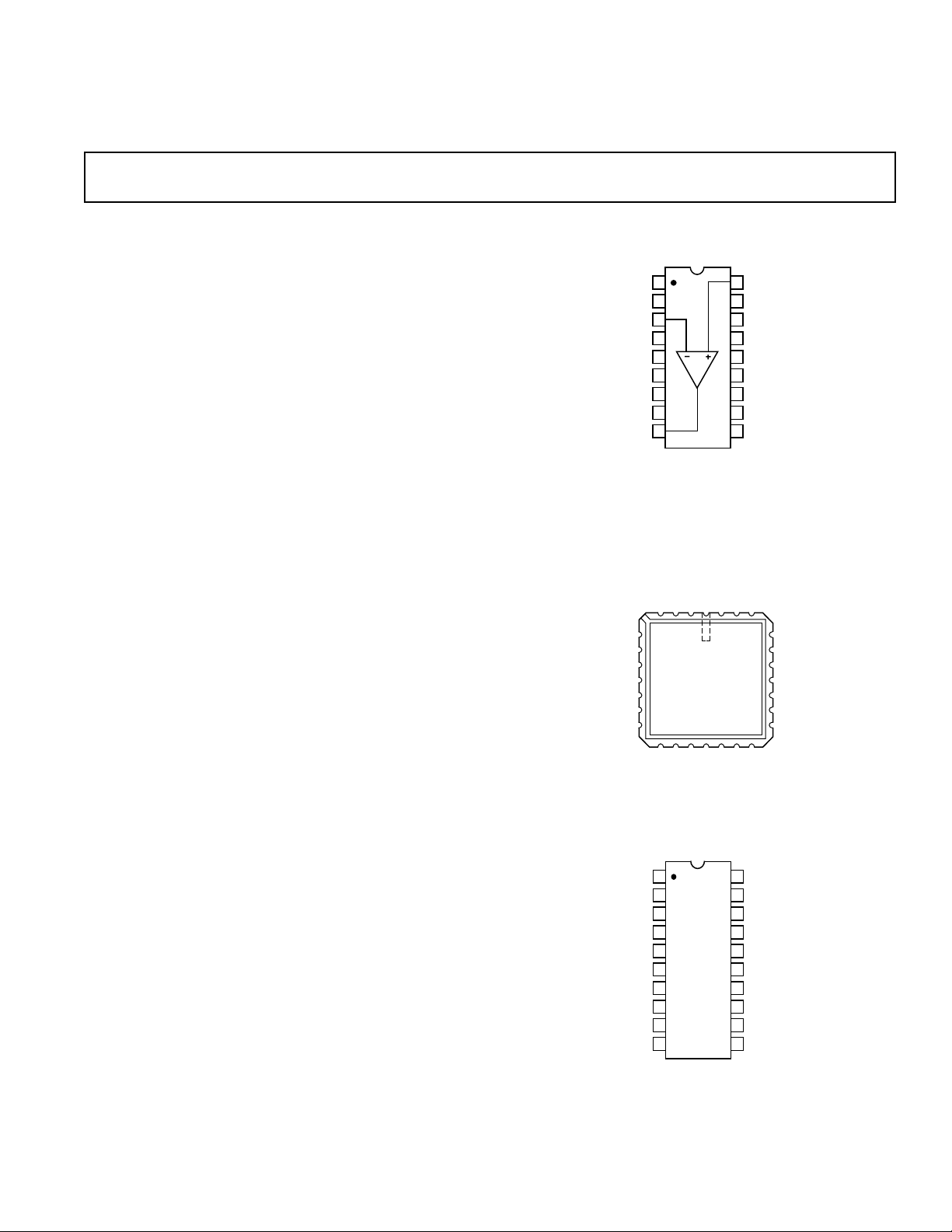
PIN CONFIGURATIONS
18-Lead Cerdip
18
+IN
17
V
IOS
16
V
NULL
IOS
15
R
S
14
R
S
13
+V
OP
12
V+
V–
11
10
–V
AMP01
G
NC
R
OP
NULL
IOS
V
+IN
NC
28 27123426
AMP01
OP
V–
NC
NC
OUT
–V
20
R
G
19
TEST PIN*
18
+IN
17
V
IOS
16
V
IOS
15
R
S
14
R
S
13
+V
OP
12
V+
11
V–
NULL
25
24
23
22
21
20
19
NULL
NULL
V
NC
R
R
+V
NC
V+
IOS
S
S
NULL
OP
V
NULL
OOS
V
NULL
OOS
TEST PIN*
SENSE
REFERENCE
OUTPUT
*MAKE NO ELECTRICAL CONNECTION
NC
V
NULL
OOS
NC
V
NULL
OOS
NC
TEST PIN*
NC = NO CONNECT
10
11
NC
*MAKE NO ELECTRICAL CONNECTION
TEST PIN*
V
NULL
OOS
V
NULL
OOS
TEST PIN*
SENSE
REFERENCE
OUTPUT
–V
*MAKE NO ELECTRICAL CONNECTION
1
R
G
2
R
G
3
–IN
4
5
6
7
8
9
TOP VIEW
(Not to Scale)
AMP01 BTC/883
28-Terminal LCC
G
–IN
R
5
6
7
8
9
TOP VIEW
(Not to Scale)
12
13 14 15 16 17 18
REF
SENSE
20-Lead SOIC
1
R
G
2
3
–IN
4
5
AMP01
TOP VIEW
6
(Not to Scale)
7
8
9
10
OP
REV. D
Information furnished by Analog Devices is believed to be accurate and
reliable. However, no responsibility is assumed by Analog Devices for its
use, nor for any infringements of patents or other rights of third parties
which may result from its use. No license is granted by implication or
otherwise under any patent or patent rights of Analog Devices.
*Protected under U.S. Patent Numbers 4,471,321 and 4,503,381.
One Technology Way, P.O. Box 9106, Norwood, MA 02062-9106, U.S.A.
Tel: 781/329-4700 World Wide Web Site: http://www.analog.com
Fax: 781/326-8703 © Analog Devices, Inc., 1999
Page 2

AMP01–SPECIFICATIONS
ELECTRICAL CHARACTERISTICS
(@ VS = ⴞ15 V, RS = 10 k⍀, RL = 2 k⍀, TA = +25ⴗC, unless otherwise noted)
AMP01A AMP01B
Parameter Symbol Conditions Min Typ Max Min Typ Max Units
OFFSET VOLTAGE
T
Input Offset Voltage V
IOS
Input Offset Voltage Drift TCV
Output Offset Voltage V
OOS
Output Offset Voltage Drift TCV
IOS
OOS
= +25°C 2050 40100 µV
A
–55°C ≤ T
≤ +125°C 4080 60150 µV
A
–55°C ≤ TA ≤ +125°C 0.15 0.3 0.3 1.0 µV/°C
T
= +25°C1326mV
A
–55°C ≤ T
RG =
≤ +125°C36610mV
A
∞
–55°C ≤ TA ≤ +125°C 2050 50120 µV/°C
Offset Referred to Input PSR G = 1000 120 130 110 120 dB
vs. Positive Supply G = 100 110 130 100 120 dB
V+ = +5 V to +15 V G = 10 95 110 90 100 dB
G = 1 75 90 70 80 dB
–55°C ≤ T
≤ +125°C
A
G = 1000 120 130 110 120 dB
G = 100 110 130 100 120 dB
G = 10 95 110 90 100 dB
G = 1 75 90 70 80 dB
Offset Referred to Input PSR G = 1000 105 125 105 115 dB
vs. Negative Supply G = 100 90 105 90 95 dB
V– = –5 V to –15 V G = 10 70 85 70 75 dB
G = 1 50 65 50 60 dB
–55°C ≤ T
≤ +125°C
A
G = 1000 105 125 105 115 dB
G = 100 90 105 90 95 dB
G = 10 70 85 70 75 dB
G = 1 50 85 50 60 dB
Input Offset Voltage Trim
Range V
Output Offset Voltage Trim
Range V
= ±4.5 V to ±18 V
S
= ±4.5 V to ±18 V
S
1
1
±6 ±6mV
±100 ±100 mV
INPUT CURRENT
T
Input Bias Current I
B
Input Bias Current Drift TCI
Input Offset Current I
OS
Input Offset Current Drift TCI
B
OS
= +25°C1426nA
A
–55°C ≤ T
≤ +125°C410615nA
A
–55°C ≤ TA ≤ +125°C 40 50 pA/°C
T
= +25°C 0.2 1.0 0.5 2.0 nA
A
–55°C ≤ T
≤ +125°C 0.5 3.0 1.0 6.0 nA
A
–55°C ≤ TA ≤ +125°C 3 5 pA/°C
INPUT
Input Resistance R
IN
Differential, G = 1000 1 1 GΩ
Differential, G ≤ 100 10 10 GΩ
Input Voltage Range IVR T
Common-Mode Rejection CMR V
Common Mode, G = 1000 20 20 GΩ
= +25°C
A
–55°C ≤ T
= ±10 V, 1 kΩ
CM
2
≤ +125°C ±10.0 ±10.0 V
A
±10.5 ±10.5 V
Source Imbalance
G = 1000 125 130 115 125 dB
G = 100 120 130 110 125 dB
G = 10 100 120 95 110 dB
G = 1 85 100 75 90 dB
–55°C ≤ T
≤ +125°C
A
G = 1000 120 125 110 120 dB
G = 100 115 125 105 120 dB
G = 10 95 115 90 105 dB
G = 1 80 95 75 90 dB
NOTES
1
V
and V
IOS
2
Refer to section on common-mode rejection.
Specifications subject to change without notice.
nulling has minimal affect on TCV
OOS
and TCV
IOS
respectively.
OOS
REV. D–2–
Page 3

AMP01
(@ VS = ⴞ15 V, RS = 10 k⍀, RL = 2 k⍀, T
ELECTRICAL CHARACTERISTICS
grades, 0ⴗC ≤ TA ≤ +70ⴗC for G grade, unless otherwise noted)
Parameter Symbol Conditions Min Typ Max Min Typ Max Units
OFFSET VOLTAGE
T
Input Offset Voltage V
IOS
Input Offset Voltage Drift TCV
Output Offset Voltage V
OOS
Output Offset Voltage Drift TCV
IOS
OOS
= +25°C 2050 40100 µV
A
≤ TA ≤ T
T
MIN
T
≤ TA ≤ T
MIN
T
= +25°C1326mV
A
≤ TA ≤ T
T
MIN
RG =
∞
T
≤ TA ≤ T
MIN
MAX
1
MAX
MAX
1
MAX
Offset Referred to Input PSR G = 1000 120 130 110 120 dB
vs. Positive Supply G = 100 110 130 100 120 dB
V+ = +5 V to +15 V G = 10 95 110 90 100 dB
G = 1 75 90 70 80 dB
≤ TA ≤ T
T
MIN
MAX
G = 1000 120 130 110 120 dB
G = 100 110 130 100 120 dB
G = 10 95 110 90 100 dB
G = 1 75 90 70 80 dB
Offset Referred to Input PSR G = 1000 110 125 105 115 dB
vs. Negative Supply G = 100 95 105 90 95 dB
V– = –5 V to –15 V G = 10 75 85 70 75 dB
G = 1 55 65 50 60 dB
≤ TA ≤ T
T
MIN
MAX
G = 1000 110 125 105 115 dB
G = 100 95 105 90 95 dB
G = 10 75 85 70 75 dB
G = 1 55 85 50 60 dB
Input Offset Voltage Trim
Range V
Output Offset Voltage Trim
Range V
= ±4.5 V to ±18 V
S
= ±4.5 V to ±18 V
S
2
2
INPUT CURRENT
T
Input Bias Current I
B
Input Bias Current Drift TCI
Input Offset Current I
OS
Input Offset Current Drift TCI
B
OS
= +25°C1426mV
A
≤ TA ≤ T
T
MIN
T
≤ TA ≤ T
MIN
T
= +25°C 0.2 1.0 0.5 2.0 mV
A
≤ TA ≤ T
T
MIN
T
≤ TA ≤ T
MIN
MAX
MAX
MAX
MAX
INPUT
Input Resistance R
IN
Differential, G = 1000 1 1 GΩ
Differential, G ≤ 100 10 10 GΩ
Input Voltage Range IVR T
Common-Mode Rejection CMR V
Common Mode, G = 1000 20 20 GΩ
= +25°C
A
T
MIN
= ±10 V, 1 kΩ
CM
3
≤ TA ≤ T
MAX
±10.5 ±10.5 V
±10.0 ±10.0 V
Source Imbalance
G = 1000 125 130 115 125 dB
G = 100 120 130 110 125 dB
G = 10 100 120 95 110 dB
G = 1 85 100 75 90 dB
≤ TA ≤ T
T
MIN
MAX
G = 1000 120 125 110 120 dB
G = 100 115 125 105 120 dB
G = 10 95 115 90 105 dB
G = 1 80 95 75 90 dB
NOTES
1
Sample tested.
2
V
and V
IOS
3
Refer to section on common-mode rejection.
Specifications subject to change without notice.
nulling has minimal affect on TCV
OOS
REV. D
and TCV
IOS
, respectively.
OOS
–3–
= +25ⴗC, –25ⴗC ≤
A
T
≤ +85ⴗC for E, F
A
AMP01E AMP01F/G
40 80 60 150 µV
0.15 0.3 0.3 1.0 µV/°C
36 610 mV
20 100 50 120 µV/°C
±6 ±6mV
±100 ±100 mV
410 615 mV
40 50 pA/°C
0.5 3.0 1.0 6.0 mV
3 5 pA/°C
Page 4

AMP01
ELECTRICAL CHARACTERISTICS
(@ VS = ⴞ15 V, RS = 10 k⍀, RL = 2 k⍀, TA = +25ⴗC, unless otherwise noted)
AMP01A/E AMP01B/F/G
Parameter Symbol Conditions Min Typ Max Min Typ Max Units
GAIN
20 × R
Gain Equation Accuracy G =
S
R
G
0.3 0.6 0.5 0.8 %
Accuracy Measured
from G = 1 to 1000
Gain Range G 0.1 10k 0.1 10k V/V
Nonlinearity G = 1000
G = 100
G = 10
G = 1
Temperature Coefficient G
TC
1 ≤ G ≤ 1000
1
1
1
1
1, 2
0.0007 0.005 0.0007 0.005 %
0.005 0.005 %
0.005 0.007 %
0.010 0.015 %
5 10 5 15 ppm°C
OUTPUT RATING
R
Output Voltage Swing V
OUT
= 2 kΩ±13.0 ±13.8 ±13.0 ±13.8 V
L
= 500 Ω±13.0 ±13.5 ±13.0 ±13.5 V
R
L
= 50 Ω±2.5 ±4.0 ±2.5 ±4.0 V
R
L
= 2 kΩ Over Temp. ±12.0 ±13.8 ±12.0 ±13.8 V
R
L
= 500 Ω
R
L
3
±12.0 ±13.5 ±12.0 ±13.5 V
Positive Current Limit Output-to-Ground Short 60 100 120 60 100 120 mA
Negative Current Limit Output-to-Ground Short 60 90 120 60 90 120 mA
Capacitive Load Stability 1 ≤ G ≤ 1000
No Oscillations
1
0.1 1 0.1 1 µF
Thermal Shutdown
Temperature Junction Temperature 165 165 °C
NOISE
Voltage Density, RTI e
Noise Current Density, RTI i
Input Noise Voltage e
n
e
n
e
n
e
n
e
n
n
n
e
n
e
n
e
n
e
n
fO = 1 kHz
G = 1000 5 5 nV/√Hz
G = 100 10 10 nV/√Hz
G = 10 59 59 nV/√Hz
G = 1 540 540 nV/√Hz
f
= 1 kHz, G = 1000 0.15 0.15 pA/√Hz
O
p-p 0.1 Hz to 10 Hz
p-p G = 1000 0.12 0.12 µV p-p
p-p G = 100 0.16 0.16 µV
p-p
p-p G = 10 1.4 1.4 µV p-p
p-p G = 1 13 13 µV p-p
Input Noise Current in p-p 0.1 Hz to 10 Hz, G = 1000 2 2 pA p-p
DYNAMIC RESPONSE
Small-Signal G = 1 570 570 kHz
Bandwidth (–3 dB) BW G = 10 100 100 kHz
G = 100 82 82 kHz
G = 1000 26 26 kHz
Slew Rate SR G = 10 3.5 4.5 3.0 4.5 V/µs
Settling Time t
S
To 0.01%, 20 V step
G = 1 12 12 µs
G = 10 13 13 µs
G = 100 15 15 µs
G = 1000 50 50 µs
NOTES
1
Guaranteed by design.
2
Gain tempco does not include the effects of gain and scale resistor tempco match.
3
–55°C ≤ TA ≤ +125°C for A/B grades, –25°C ≤ TA ≤ +85°C for E/F grades, 0°C ≤ TA ≤ 70°C for G grades.
Specifications subject to change without notice.
–4–
REV. D
Page 5
AMP01
ELECTRICAL CHARACTERISTICS
(@ VS = ⴞ15 V, RS = 10 k⍀, RL = 2 k⍀, TA = +25ⴗC, unless otherwise noted)
AMP01A/E AMP01B/F/G
Parameter Symbol Conditions Min Typ Max Min Typ Max Units
SENSE INPUT
Input Resistance R
Input Current I
IN
IN
Referenced to V– 280 280 µA
35 50 65 35 50 65 kΩ
Voltage Range (Note 1) –10.5 +15 –10.5 +15 V
REFERENCE INPUT
Input Resistance R
Input Current I
IN
IN
Referenced to V– 280 280 µA
35 50 65 35 50 65 kΩ
Voltage Range (Note 1) –10.5 +15 –10.5 +15 V
Gain to Output 1 1 V/V
POWER SUPPLY –25°C ≤ T
Supply Voltage Range V
Quiescent Current I
NOTE
1
Guaranteed by design.
Specifications subject to change without notice.
≤ +85°C for E/F Grades, –55°C ≤ TA ≤ +125°C for A/B Grades
A
S
V
S
Q
I
Q
+V linked to +V
–V linked to –V
+V linked to +V
–V linked to –V
OP
OP
OP
OP
±4.5 ±18 ±4.5 ±18 V
±4.5 ±18 ±4.5 ±18 V
3.0 4.8 3.0 4.8 mA
3.4 4.8 3.4 4.8 mA
ORDERING GUIDE
Model Temperature Range Package Description Package Option
AMP01AX –55°C to +125°C 18-Lead Cerdip Q-18
AMP01AX/883C –55°C to +125°C 18-Lead Cerdip Q-18
AMP01BTC/883C –55°C to +125°C 28-Terminal LCC E-28A
AMP01BX –55°C to +125°C 18-Lead Cerdip Q-18
AMP01BX/883C –55°C to +125°C 18-Lead Cerdip Q-18
AMP01EX –25°C to +85°C 18-Lead Cerdip Q-18
AMP01FX –25°C to +85°C 18-Lead Cerdip Q-18
AMP01GBC Die
AMP01GS 0°C to +70°C 20-Lead SOIC R-20
AMP01GS-REEL 0°C to +70°C13" Tape and Reel R-20
AMP01NBC Die
5962-8863001VA* –55°C to +125°C 18-Lead Cerdip Q-18
5962-88630023A* –55°C to +125°C 28-Terminal LCC E-28A
5962-8863002VA* –55°C to +125°C 18-Lead Cerdip Q-18
*Standard military drawing available.
REV. D
DICE CHARACTERISTICS
Die Size 0.111 × 0.149 inch, 16,539 sq. mils
(2.82 × 3.78 mm, 10.67 sq. mm)
–5–
1. R
G
2. R
G
3. –INPUT
4. V
NULL
OOS
NULL
5. V
OOS
6. TEST PIN*
7. SENSE
8. REFERENCE
9. OUTPUT
*MAKE NO ELECTRICAL CONNECTION
10. V– (OUTPUT)
11. V–
12. V+
13. V+ (OUTPUT)
14. R
S
15. R
S
16. V
NULL
IOS
NULL
17. V
IOS
18. +INPUT
Page 6
AMP01
WARNING!
ESD SENSITIVE DEVICE
WAFER TEST LIMITS
(@ VS = ⴞ15 V, RS = 10 k⍀, RL = 2 k⍀, TA = +25ⴗC, unless otherwise noted)
AMP01NBC AMP01GBC
Parameter Symbol Conditions Limit Limit Units
Input Offset Voltage V
Output Offset Voltage V
IOS
OOS
60 120 µV max
4 8 mV max
Offset Referred to Input PSR V+ = +5 V to +15 V dB min
vs. Positive Supply G = 1000 120 110 dB min
G = 100 110 100 dB min
G = 10 95 90 dB min
G = 1 75 70 dB min
Offset Referred to Input PSR V– = –5 V to –15 V dB min
vs. Negative Supply G = 1000 105 105 dB min
G = 100 90 90 dB min
G = 10 70 70 dB min
G = 1 50 50 dB min
Input Bias Current I
Input Offset Current I
B
OS
48nA max
13nA max
Input Voltage Range IVR Guaranteed by CMR Tests ±10 ±10 V min
Common Mode Rejection CMR V
= ±10 V dB min
CM
G = 1000 125 115 dB min
G = 100 120 110 dB min
G = 10 100 95 dB min
G = 1 85 75 dB min
Gain Equation Accuracy G =
Output Voltage Swing V
V
V
OUT
OUT
OUT
R
= 2 kΩ±13 ±13 V min
L
R
= 500 Ω±13 ±13 V min
L
R
= 50 Ω±2.5 ±2.5 V min
L
S
R
G
0.6 0.8 % max
20 × R
Output Current Limit Output to Ground Short ±60 ±60 mA min
Output Current Limit Output to Ground Short ±120 ±120 mA max
Quiescent Current I
NOTE
Electrical tests are performed at wafer probe to the limits shown. Due to variations in assembly methods and normal yield loss, yield after packaging is not guaranteed
for standard product dice. Consult factory to negotiate specifications based on dice lot qualification through sample lot assembly and testing.
Q
+V Linked to +V
–V Linked to –V
OP
OP
4.8 4.8 mA max
4.8 4.8 mA max
V
IOS
NULL
A1
250V
–IN
250V
+IN
REFERENCE
R1
47.5kV
R2
2.5kV
Q1 Q2
R
GAIN
R
SCALE
V
OOS
NULL
A3A2
Figure 1. Simplified Schematic
CAUTION
ESD (electrostatic discharge) sensitive device. Electrostatic charges as high as 4000 V readily
accumulate on the human body and test equipment and can discharge without detection.
Although the AMP01 features proprietary ESD protection circuitry, permanent damage may
occur on devices subjected to high energy electrostatic discharges. Therefore, proper ESD
precautions are recommended to avoid performance degradation or loss of functionality.
–6–
R3
47.5kV
R4
2.5kV
V+
+V
OP
OUTPUT
–V
OP
SENSE
V–
REV. D
Page 7

AMP01
ELECTRICAL CHARACTERISTICS
(@ VS = ⴞ15 V, RS = 10 k⍀, RL = 2 k⍀, TA = +25ⴗC, unless otherwise noted)
AMP01NBC AMP01GBC
Parameter Symbol Conditions Typical Typical Units
Input Offset Voltage Drift TCV
Output Offset Voltage Drift TCV
Input Bias Current Drift TCI
Input Offset Current Drift TCI
B
OS
IOS
OOS
RG =
∞
0.15 0.30 µV/°C
20 50 µV/°C
40 50 pA/°C
3 5 pA/°C
Nonlinearity G = 1000 0.0007 0.0007 %
Voltage Noise Density e
Current Noise Density i
Voltage Noise e
n
n
p-p G = 1000
n
G = 1000
= 1 kHz 5 5 nV/√Hz
f
O
G = 1000
= 1 kHz 0.15 0.15 pA/√Hz
f
O
0.1 Hz to 10 Hz 0.12 0.12 µV p-p
Current Noise i
p-p G = 1000 2 2 pA p-p
n
0.1 Hz to 10 Hz
Small-Signal Bandwidth (–3 dB) BW G = 1000 26 26 kHz
Slew Rate SR G = 10 4.5 4.5 V/µs
Settling Time t
S
To 0.01%, 20 V Step
G = 1000 50 50 µs
NOTE
Electrical tests are performed at wafer probe to the limits shown. Due to variations in assembly methods and normal yield loss, yield after packaging is not guaranteed
for standard product dice. Consult factory to negotiate specifications based on dice lot qualification through sample lot assembly and testing.
REV. D
–7–
Page 8

AMP01
TEMPERATURE – 8C
–75 –50 150
–25 0 25 75 100 12550
OUTPUT OFFSET VOLTAGE – mV
5
4
–4
0
–1
–2
–3
3
1
2
–5
VS = 615V
POWER SUPPLY VOLTAGE – Volts
INPUT BIAS CURRENT – nA
2.0
1.5
–1.5
0
65 620610 615
0.5
0
–0.5
–1.0
1.0
TA = +258C
FREQUENCY – Hz
COMMON-MODE REJECTION – dB
140
0
1 10 100k100 1k 10k
120
100
80
60
40
20
VCM = 2V p-p
V
S
= 615V
T
A
= +258C
G = 1000
G = 100
G = 1
G = 10
–Typical Performance Characteristics
50
VS = 615V
40
30
20
10
0
–10
–20
INPUT OFFSET VOLTAGE – mV
–30
–40
–25 0 25 75 100 12550
–75 –50 150
TEMPERATURE – 8C
Figure 2. Input Offset Voltage
vs. Temperature
2.5
2.0
1.5
1.0
0.5
0
–0.5
OUTPUT OFFSET VOLTAGE CHANGE – mV
–1.0
0
65 625610 615 620
POWER SUPPLY VOLTAGE – Volts
TA = +258C
Figure 5. Output Offset Voltage
Change vs. Supply Voltage
8
TA = +258C
6
4
2
0
–2
INPUT OFFSET VOLTAGE – mV
–4
–6
0
65 620610 615
POWER SUPPLY VOLTAGE – Volts
UNIT NO.
1
2
3
4
Figure 3. Input Offset Voltage
vs. Supply Voltage
5
VS = 615V
4
3
2
1
0
INPUT BIAS CURRENT – nA
–1
–2
–75 –50 150
0
–25
25 75 100 12550
TEMPERATURE – 8C
Figure 6. Input Bias Current
vs. Temperature
Figure 4. Output Offset Voltage
vs. Temperature
Figure 7. Input Bias Current
vs. Supply Voltage
0.8
VS = 615V
0.6
0.4
0.2
0.0
–0.2
INPUT OFFSET CURRENT – nA
–0.4
–0.6
–75 –50 150
–25025 75 100 12550
TEMPERATURE – 8C
Figure 8. Input Offset Current
vs. Temperature
140
VS = 615V
= +258C
T
A
130
120
110
COMMON-MODE REJECTION – dB
100
1 10k
10 100 1k
VOLTAGE GAIN – G
Figure 9. Common-Mode Rejection
vs. Voltage Gain
–8–
Figure 10. Common-Mode Rejection
vs. Frequency
REV. D
Page 9

AMP01
FREQUENCY – Hz
POWER SUPPLY REJECTION – dB
140
0
1 10 100k100 1k 10k
120
100
80
60
40
20
VS = 615V
T
A
= +258C
DV
S
= 61V
G = 1000
G = 100
G = 10
G = 1
FREQUENCY – Hz
OUTPUT IMPEDANCE – V
100
10 100 1M1k 10k 100k
10
1.0
0.1
0.01
0.001
VS = 615V
I
OUT
= 20mA p-p
G = 1000
G = 1
LOAD RESISTANCE – V
TOTAL HARMONIC DISTORTION – %
0.02
0.01
10k100 1k
0
VS = 615V
G = 100
f = 1kHz
V
OUT
= 20V p-p
16
VDM = 0
14
12
10
8
6
4
2
COMMON-MODE INPUT VOLTAGE – Volts
0
–75 –50 150
VS = 615V
VS = 610V
VS = 65V
–25025 75 100 12550
TEMPERATURE – 8C
Figure 11. Common-Mode Voltage
Range vs. Temperature
18
VS = 615V
16
14
12
10
8
6
4
OUITPUT VOLTAGE – Volts
2
0
10 100 1k
LOAD RESISTANCE – V
10k
Figure 14. Maximum Output Voltage
vs. Load Resistance
140
120
100
80
60
40
20
POWER SUPPLY REJECTION – dB
0
1 10 100k100 1k 10k
G = 1000
G = 10
FREQUENCY – Hz
G = 1
VS = 615V
T
A
DV
G = 100
= +258C
= 61V
S
Figure 12. Positive PSR
vs. Frequency
30
25
20
15
10
5
PEAK-TO-PEAK AMPLITUDE – Volts
0
100 1M
1k 10k 100k
FREQUENCY – Hz
VS = 615V
= 2kV
R
L
Figure 15. Maximum Output Swing
vs. Frequency
Figure 13. Negative PSR
vs. Frequency
Figure 16. Closed-Loop Output
Impedance vs. Frequency
80
60
40
20
0
VOLTAGE GAIN – dB
–20
–40
Figure 17. Closed-Loop Voltage
Gain vs. Frequency
REV. D
101
VS = 615V
= +258C
G = 1000
G = 100
G = 10
G = 1
100 1M
1k 10k 100k
FREQUENCY – Hz
T
A
0.08
VS = 615V
0.07
= 600V
R
L
= 20V p-p
V
OUT
0.06
0.05
0.04
0.03
0.02
0.01
TOTAL HARMONIC DISTORTION – %
0
10 100 1k
FREQUENCY – Hz
G = 1000
G = 10
G = 100
G = 1
10k
Figure 18. Total Harmonic Distortion
vs. Frequency
–9–
Figure 19. Total Harmonic Distortion
vs. Load Resistance
Page 10

AMP01
VOLTAGE GAIN – G
SETTLING TIME – ms
70
40
1k
50
1 10 100
60
30
20
10
VS = 615V
20V STEP
POWER SUPPLY VOLTAGE – Volts
POSITIVE SUPPLY CURRENT – mA
8
7
0
0
65 620
610 615
4
3
2
1
6
5
TA = +258C
TEMPERATURE – 8C
NEGATIVE SUPPLY CURRENT – mA
–6
0
–75 –50 150–25 0 25 75 100 12550
–5
–4
–3
–2
–1
VS = 615V
V
SENSE
= V
REF
= 0V
6
VS = 615V
5
4
3
2
SLEW RATE – V/ms
1
0
1 10 100
VOLTAGE GAIN – G
Figure 20. Slew Rate vs.
Voltage Gain
15
10
5
VOLTAGE NOISE – nV/ Hz
G = 1000
6
5
4
3
2
SLEW RATE – V/ms
1
1k
0
100p 1m
1n 10n 100n
LOAD CAPACITANCE – F
Figure 21. Slew Rate vs.
Load Capacitance
1k
100
10
VOLTAGE NOISE – nV/ Hz
VS = 615V
VS = 615V
f = 1kHz
Figure 22. Settling Time to 0.01%
vs. Voltage Gain
0
1 10k
10 100 1k
FREQUENCY – Hz
Figure 23. Voltage Noise Density
vs. Frequency
–8
TA = +258C
–7
–6
–5
–4
–3
–2
–1
NEGATIVE SUPPLY CURRENT – mA
0
0
65 620
POWER SUPPLY VOLTAGE – Volts
Figure 26. Negative Supply Current
vs. Supply Voltage
610 615
1
1 10 100
VOLTAGE GAIN – G
1k
Figure 24. RTI Voltage Noise
Density vs. Gain
6
VS = 615V
5
4
3
2
1
POSITIVE SUPPLY CURRENT – mA
0
–75 –50 150–25 0 25 75 100 12550
TEMPERATURE – 8C
Figure 27. Positive Supply Current
vs. Temperature
–10–
Figure 25. Positive Supply Current
vs. Supply Voltage
Figure 28. Negative Supply Current
vs. Temperature
REV. D
Page 11

AMP01
INPUT AND OUTPUT OFFSET VOLTAGES
Instrumentation amplifiers have independent offset voltages
associated with the input and output stages. While the initial
offsets may be adjusted to zero, temperature variations will
cause shifts in offsets. Systems with auto-zero can correct for
offset errors, so initial adjustment would be unnecessary. However, many high-gain applications don’t have auto zero. For
these applications, both offsets can be nulled, which has minimal effect on TCV
and TCV
IOS
OOS
The input offset component is directly multiplied by the amplifier gain, whereas output offset is independent of gain. Therefore, at low gain, output-offset errors dominate, while at high
gain, input-offset errors dominate. Overall offset voltage, V
OS
,
referred to the output (RTO) is calculated as follows;
V
where V
(RTO) = (V
OS
and V
IOS
OOS
× G) + V
IOS
OOS
are the input and output offset voltage
(1)
specifications and G is the amplifier gain. Input offset nulling
alone is recommended with amplifiers having fixed gain above
50. Output offset nulling alone is recommended when gain is
fixed at 50 or below.
In applications requiring both initial offsets to be nulled, the
input offset is nulled first by short-circuiting R
, then the output
G
offset is nulled with the short removed.
The overall offset voltage drift TCV
, referred to the output, is
OS
a combination of input and output drift specifications. Input
offset voltage drift is multiplied by the amplifier gain, G, and
summed with the output offset drift;
TCV
where TCV
(RTO) = (TCV
OS
is the input offset voltage drift, and TCV
IOS
× G) + TCV
IOS
OOS
OOS
(2)
is
the output offset voltage specification. Frequently, the amplifier
drift is referred back to the input (RTI), which is then equivalent to an input signal change;
TCV
TCV
OS
(RTI) = TCV
IOS
OOS
G
(3)
For example, the maximum input-referred drift of an AMP01 EX
set to G = 1000 becomes;
100
TCVOS (RTI ) = 0.3
µ
V/°C +
µVC/°
= 0.4
µ
1000
V/°C max
INPUT BIAS AND OFFSET CURRENTS
Input transistor bias currents are additional error sources that
can degrade the input signal. Bias currents flowing through the
signal source resistance appear as an additional offset voltage.
Equal source resistance on both inputs of an IA will minimize
offset changes due to bias current variations with signal voltage
and temperature. However, the difference between the two bias
currents, the input offset current, produces a nontrimmable
error. The magnitude of the error is the offset current times the
source resistance.
A current path must always be provided between the differential
inputs and analog ground to ensure correct amplifier operation.
Floating inputs, such as thermocouples, should be grounded
close to the signal source for best common-mode rejection.
GAIN
The AMP01 uses two external resistors for setting voltage gain
over the range 0.1 to 10,000. The magnitudes of the scale resis-
, and gain-set resistor, RG, are related by the formula:
tor, R
S
G = 20 × R
, where G is the selected voltage gain (refer to
S/RG
Figure 29).
V+
S
15
S
R
G
13
10
12
11
V–
SENSE
7
9
8
REFERENCE
OUTPUT
+IN
–IN
VOLTAGE GAIN, G =
18
1
R
G
2
3
R
14
AMP01
20 3 R
( )
Figure 29. Basic AMP01 Connections for Gains
0.1 to 10,000
The magnitude of RS affects linearity and output referred errors.
Circuit performance is characterized using R
operating on ±15 volt supplies and driving a ±10 volt output. R
= 10 kΩ when
S
S
may be reduced to 5 kΩ in many applications particularly when
operating on ±5 volt supplies or if the output voltage swing is
limited to ±5 volts. Bandwidth is improved with R
= 5 kΩ and
S
this also increases common-mode rejection by approximately
6 dB at low gain. Lowering the value below 5 kΩ can cause
instability in some circuit configurations and usually has no
advantage. High voltage gains between two and ten thousand
would require very low values of R
= 2000 we get R
A
V
limit for R
. Below 100 Ω, mismatch of wirebond and resistor
G
= 100 Ω; this value is the practical lower
G
. For R
G
= 10 kΩ and
S
temperature coefficients will introduce significant gain tempco
errors. Therefore, for gains above 2,000, R
constant at 100 Ω and R
10,000 is obtained with R
increased. The maximum gain of
S
set to 50 kΩ.
S
should be kept
G
Metal-film or wirewound resistors are recommended for best
results. The absolute values and TCs are not too important,
only the ratiometric parameters.
AC amplifiers require good gain stability with temperature and
time, but dc performance is unimportant. Therefore, low cost
metal-film types with TCs of 50 ppm/°C are usually adequate
for R
and RG. Realizing the full potential of the AMP01’s offset
S
voltage and gain stability requires precision metal-film or wire-
wound resistors. Achieving a 15 ppm/°C gain tempco at all gains
requires R
and RG temperature coefficient matching to
S
5 ppm/°C or better.
REV. D
–11–
Page 12

AMP01
1M
VS = 615V
100k
R
10k
RESISTANCE – V
1k
100
1 10k
10 100 1k
VOLTAGE GAIN
S
R
G
Figure 30. RG and RS Selection
Gain accuracy is determined by the ratio accuracy of RS and R
G
combined with the gain equation error of the AMP01 (0.6%
max for A/E grades).
All instrumentation amplifiers require attention to layout so
thermocouple effects are minimized. Thermocouples formed
between copper and dissimilar metals can easily destroy the
TCV
performance of the AMP01 which is typically
OS
0.15 µV/°C. Resistors themselves can generate thermoelectric
EMF’s when mounted parallel to a thermal gradient. “Vishay”
resistors are recommended because a maximum value for thermoelectric generation is specified. However, where thermal
gradients are low and gain TCs of 20 ppm–50 ppm are sufficient, general-purpose metal-film resistors can be used for R
G
and RS.
COMMON-MODE REJECTION
Ideally, an instrumentation amplifier responds only to the difference between the two input signals and rejects commonmode voltages and noise. In practice, there is a small change in
output voltage when both inputs experience the same commonmode voltage change; the ratio of these voltages is called the
common-mode gain. Common-mode rejection (CMR) is the
logarithm of the ratio of differential-mode gain to commonmode gain, expressed in dB. CMR specifications are normally
measured with a full-range input voltage change and a specified
source resistance unbalance.
The current-feedback design used in the AMP01 inherently
yields high common-mode rejection. Unlike resistive feedback
designs, typified by the three-op-amp IA, the CMR is not degraded by small resistances in series with the reference input. A
slight, but trimmable, output offset voltage change results from
resistance in series with the reference input.
The common-mode input voltage range, CMVR, for linear
operation may be calculated from the formula:
CMVR = ±
IVR –
|V
OUT
2G
|
(4)
IVR is the data sheet specification for input voltage range; V
OUT
is the maximum output signal; G is the chosen voltage gain. For
example, at +25°C, IVR is specified as ±10.5 volt minimum
with ±15 volt supplies. Using a ±10 volt maximum swing out-
put and substituting the figures in (4) simplifies the formula to:
CMVR = ±
10.5 –
5
G
(5)
For all gains greater than or equal to 10, CMVR is ±10 volt
minimum; at gains below 10, CMVR is reduced.
ACTIVE GUARD DRIVE
Rejection of common-mode noise and line pick-up can be improved by using shielded cable between the signal source and
the IA. Shielding reduces pick-up, but increases input capacitance, which in turn degrades the settling-time for signal
changes. Further, any imbalance in the source resistance between the inverting and noninverting inputs, when capacitively
loaded, converts the common-mode voltage into a differential
voltage. This effect reduces the benefits of shielding. AC
common-mode rejection is improved by “bootstrapping” the
input cable capacitance to the input signal, a technique called
“guard driving.” This technique effectively reduces the input
capacitance. A single guard-driving signal is adequate at gains
above 100 and should be the average value of the two inputs.
The value of external gain resistor R
tors R
and RG2; the center tap provides the required signal to
G1
is split between two resis-
G
drive the buffer amplifier (Figure 31).
GROUNDING
The majority of instruments and data acquisition systems have
separate grounds for analog and digital signals. Analog ground
may also be divided into two or more grounds which will be tied
together at one point, usually the analog power-supply ground.
In addition, the digital and analog grounds may be joined, normally at the analog ground pin on the A-to-D converter. Following this basic grounding practice is essential for good circuit
performance (Figure 32).
Mixing grounds causes interactions between digital circuits and
the analog signals. Since the ground returns have finite resistance and inductance, hundreds of millivolts can be developed
between the system ground and the data acquisition components. Using separate ground returns minimizes the current flow
in the sensitive analog return path to the system ground point.
Consequently, noisy ground currents from logic gates do not
interact with the analog signals.
Inevitably, two or more circuits will be joined together with their
grounds at differential potentials. In these situations, the differential input of an instrumentation amplifier, with its high CMR,
can accurately transfer analog information from one circuit to
another.
SENSE AND REFERENCE TERMINALS
The sense terminal completes the feedback path for the instrumentation amplifier output stage and is normally connected
directly to the output. The output signal is specified with respect to the reference terminal, which is normally connected to
analog ground.
–12–
REV. D
Page 13

GUARD
DRIVE
–IN
SIGNAL
GROUND
VOLTAGE GAIN, G =
AV = 500 WITH COMPONENTS SHOWN
+IN
R2
1MV
+15V
7
6
741
4
–15V
20 3 R
S
( )
R
G1
2
3
200V
200V
R1
1MV
AMP01
+15V
C3
0.047mF
R
S
10kV
S
IOS
VR2
NC
14
R
S
AMP01
V
OOS
NULL
4
17
100kV
15
R
18
R
G3
R
G2
R
G1
400V
1
R
G
2
R
G
3
V
NULL
16
100kV
6
VR1
*
C1
R4
13
10
5
0.047mF
12
7
V+
V–
8
11
+
C5
10mF
SENSE
*
R5
9
OUTPUT
*
*SOLDER LINK
*
R3
C4
0.047mF
+
C6
10mF
C2
0.047mF
*
REFERENCE
GROUND
–15V
Figure 31. AMP01 Evaluation Circuit Showing Guard-Drive Connection
DIGITAL
POWER SUPPLY
CC
ANALOG
GROUND
ADC
AMP01
CC
OUTPUT
REFERENCE
7
8
POWER SUPPLY
9
ANALOG
HOLD
CAPACITOR
–15V+15V 0V
CC
SMP-11
SAMPLE AND HOLD
0V +5V
DIGITAL
GROUND
C = 0.047mF CERAMIC CAPACITORS
Figure 32. Basic Grounding Practice
4.7mF
DIGITAL
GROUND
+
C
DIGITAL
DATA
OUTPUT
REV. D
–13–
Page 14

AMP01
If heavy output currents are expected and the load is situated
some distance from the amplifier, voltage drops due to track or
wire resistance will cause errors. Voltage drops are particularly
troublesome when driving 50 Ω loads. Under these conditions,
the sense and reference terminals can be used to “remote sense”
the load as shown in Figure 33. This method of connection puts
the I×R drops inside the feedback loop and virtually eliminates
the error. An unbalance in the lead resistances from the sense
and reference pins does not degrade CMR, but will change the
output offset voltage. For example, a large unbalance of 3 Ω will
change the output offset by only 1 mV.
DRIVING 50 ⍀ LOADS
Output currents of 50 mA are guaranteed into loads of up to
50 Ω and 26 mA into 500 Ω. In addition, the output is stable
and free from oscillation even with a high load capacitance. The
V+
+IN
–IN
R
S
14
18
1
R
G
2
3
15
AMP01
12
13
10
11
IN4148 DIODES ARE OPTIONAL. DIODES LIMIT THE OUTPUT
*
VOLTAGE EXCURSION IF SENSE AND/OR REFERENCE LINES
BECOME DISCONNECTED FROM THE LOAD.
SENSE
7
9
8
REFERENCE
*
*
combination of these unique features in an instrumentation
amplifier allows low-level transducer signals to be conditioned
and directly transmitted through long cables in voltage or current form. Increased output current brings increased internal
dissipation, especially with 50 Ω loads. For this reason, the
power-supply connections are split into two pairs; pins 10 and
13 connect to the output stage only and pins 11 and 12 provide
power to the input and following stages. Dual supply pins allow
dropper resistors to be connected in series with the output stage
so excess power is dissipated outside the package. Additional
decoupling is necessary between pins 10 and 13 to ground to
maintain stability when dropper resistors are used. Figure 34
shows a complete circuit for driving 50 Ω loads.
TWISTED
PAIRS
REMOTE
LOAD
V–
Figure 33. Remote Load Sensing
POWER BANDWIDTH, G = 100, 130kHz
POWER BANDWIDTH, G = 10, 200kHz
T.H.D.~0.04% @ 1kHz, 2Vrms
+IN
–IN
VOLTAGE GAIN, G =
RESISTERS R1 AND R2 REDUCE IC DISSIPATION
20 3 R
( )
18
R
G
S
R
G
R
5kV
14
1
2
3
Figure 34. Driving 50 Ω Loads
OUTPUT
GROUND
S
15
AMP01
12
11
R1
130V
1W
130V
1W
+15V
0.047mF
C1
0.047mF
SENSE
13
7
9
8
10
REFERENCE
C2
0.047mF
R2
0.047mF
V
OUT
63V MAX
50V
LOAD
–15V
–14–
REV. D
Page 15

AMP01
V
OUT
+15V
+IN
–IN
AMP01
9.1V 1W
ZENERS
100V
1W
*
100V
1W*
OPTIONAL PROTECTION
RESISTORS, SEE TEXT.
*
LINEAR INPUT RANGE,
65V MAXIMUM
DIFFERENTIAL PROTECTION
TO 630V
–15V
HEATSINKING
To maintain high reliability, the die temperature of any IC
should be kept as low as practicable, preferably below 100°C.
Although most AMP01 application circuits will produce very
little internal heat — little more than the quiescent dissipation
of 90 mW—some circuits will raise that to several hundred
milliwatts (for example, the 4-20 mA current transmitter application, Figure 37). Excessive dissipation will cause thermal
shutdown of the output stage thus protecting the device from
damage. A heatsink is recommended in power applications to
reduce the die temperature.
Several appropriate heatsinks are available; the Thermalloy
6010B is especially easy to use and is inexpensive. Intended for
dual-in-line packages, the heatsink may be attached with a
cyanoacrylate adhesive. This heatsink reduces the thermal resistance between the junction and ambient environment to ap-
proximately 80°C/W. Junction (die) temperature can then be
calculated by using the relationship:
where TJ and TA are the junction and ambient temperatures
respectively, θ
ent, and P
OVERVOLTAGE PROTECTION
Instrumentation amplifiers invariably sit at the front end of
instrumentation systems where there is a high probability of
exposure to overloads. Voltage transients, failure of a transducer, or removal of the amplifier power supply while the signal
source is connected may destroy or degrade the performance of
an unprotected amplifier. Although it is impractical to protect
an IC internally against connection to power lines, it is relatively
easy to provide protection against typical system overloads.
The AMP01 is internally protected against overloads for gains
of up to 100. At higher gains, the protection is reduced and
some external measures may be required. Limited internal overload protection is used so that noise performance would not be
significantly degraded.
AMP01 noise level approaches the theoretical noise floor of the
input stage which would be 4 nV/√Hz at 1 kHz when the gain is
set at 1000. Noise is the result of shot noise in the input devices
and Johnson noise in the resistors. Resistor noise is calculated
from the values of R
protection resistors (250 Ω). Active loads for the input transistors contribute less than 1 nV/√Hz of noise. The measured noise
level is typically 5 nV/√Hz.
Diodes across the input transistor’s base-emitter junctions,
combined with 250 Ω input resistors and R
differential inputs of up to ±20 V for gains of up to 100. The
diodes also prevent avalanche breakdown that would degrade
the I
gains above 100 limits the maximum input overload protection
to ±10 V.
TJ– T
P
=
d
is the thermal resistance from junction to ambi-
JA
is the device’s internal dissipation.
d
(200 Ω at a gain of 1000) and the input
G
and IOS specifications. Decreasing the value of RG for
B
A
θ
JA
, protect against
G
External series resistors could be added to guard against higher
voltage levels at the input, but resistors alone increase the input
noise and degrade the signal-to-noise ratio, especially at high
gains.
Protection can also be achieved by connecting back-to-back
9.1 V Zener diodes across the differential inputs. This technique
does not affect the input noise level and can be used down to a
gain of 2 with minimal increase in input current. Although
voltage-clamping elements look like short circuits at the limiting
voltage, the majority of signal sources provide less than 50 mA,
producing power levels that are easily handled by low-power
Zeners.
Simultaneous connection of the differential inputs to a low
impedance signal above 10 V during normal circuit operation is
unlikely. However, additional protection involves adding 100 Ω
current-limiting resistors in each signal path prior to the voltage
clamp, the resistors increase the input noise level to just
5.4 nV/√Hz (refer to Figure 35).
Input components, whether multiplexers or resistors, should be
carefully selected to prevent the formation of thermocouple
junctions that would degrade the input signal.
Figure 35. Input Overvoltage Protection for Gains
2 to 10,000
POWER SUPPLY CONSIDERATIONS
Achieving the rated performance of precision amplifiers in a
practical circuit requires careful attention to external influences.
For example, supply noise and changes in the nominal voltage
directly affect the input offset voltage. A PSR of 80 dB means
that a change of 100 mV on the supply, not an uncommon
value, will produce a 10 µV input offset change. Consequently,
care should be taken in choosing a power unit that has a low
output noise level, good line and load regulation, and good
temperature stability.
REV. D
–15–
Page 16

AMP01
+IN
–IN
+15V
0.047mF
18
12
1
R
G
R
V
G
IN
2kV
2
3
AMP01
R
G
R
S
14
R
2kV
V+
V–
11
R
S
15
–15V
S
13
10
R
TRIM
SENSE
7
9
8
REFERENCE
0.047mF
OUT
R2
200V
COMPLIANCE, TYPICALLY 610V
LINEARITY ~0.01%
OUTPUT RESISTANCE AT 20mA ~5MV
POWER BANDWIDTH (–3dB) ~60kHz
INTO 500V LOAD
R1
100V
I
OUT
R1 = 100V FOR I
V
= 6100mV FOR 620mA FULL SCALE
IN
= V
IN
6I
OUT
20 3 R
S
( )
RG 3 R1
= 620mA
OUT
Figure 36. High Compliance Bipolar Current Source with 13-Bit Linearity
ALL RESISTORS 1% METAL FILM
+15V
TO +30V
I
OUT
4mA TO 20mA
–5V
+IN
–IN
R
S
2kV
14
R
S
18
1
R
G
R
G
2.75kV
2
R
G
3
0V
15
R
12
S
V+
AMP01
V–
11
0.047mF
COMPLIANCE OF I
DIFFERENTIAL INPUT OF 100mV FOR 16mA SPAN
OUTPUT RESISTANCE ~5MV AT I
LINEARITY 0.01% OF SPAN
0.047mF
R3
100V
13
7
9
8
R5
10
OUT
2.21kV
R4
100V
, +20V WITH +30V SUPPLY (OUTPUT w.r.t. 0V)
OUT
200V
R
OUT
500V
ZERO TRIM
= 20mA
R2
TRIM
R6
R1
100V
2
4
REF-02
6
Figure 37. 13-Bit Linear 4–20 mA Transmitter Constructed by Adding a Voltage Reference.
Thermocouple Signals Can Be Accepted Without Preamplification.
–16–
REV. D
Page 17

AMP01
+15V
V
OUT
(610V INTO 10V)
GND
–15V
R
+IN
–IN
VOLTAGE GAIN, G = 100
POWER BANDWIDTH (–3dB), 60kHz
QUIESCENT CURRENT, 4mA
LINEARITY
~0.01% @ FULL OUTPUT INTO 10V
18
1
R
G
R
G
2
R
G
3
10kV
14
S
15
R
S
AMP01
V+
V–
0.047mF
12
11
0.047mF
13
10
+
10mF
SENSE
7
9
8
REFERENCE
+
2N4921
0.047mF
100V
2N4918
Figure 38. Adding Two Transistors Increases Output Current to ±1 A Without Affecting the Quiescent Current of 4 mA.
Power Bandwidth is 60 kHz.
+IN
–IN
+15V
6
27kV
+15V
7
4
–15V
IC2
47kV
47kV
47kV
47kV
3
2
2.7kV
Q1, Q2...........J110
Q3, Q4, Q5....J107
IC1 ...............CMP-04
IC2 ...............OP15GZ
200kV 20kV 2kV 196V
Q2
Q1
3
4
6
8
10
G1 G10 G100 G1000
IC1
57911
TTL COMPATIBLE INPUTS
Q3
18
1
Q4
Q5
2
3
131412
++++
12
R
R
G
AMP01
V
IOS
R
G
NULL
16
10kV
14
S
17
R
S
V
NULL
R
OOS
4
100kV100kV
+15V
0.047mF
15
12
S
V+
11
5
–15V
SENSE
13
7
9
V–
8
10
REFERENCE
0.047mF
LINEARITY~0.005%, G = 10 AND 100
~0.02%, G = 1 AND 1000
GAIN ACCURACY, UNTRIMMED~0.5%
SETTLING TIME TO 0.01%, ALL GAINS,
LESS THAN 75ms
GAIN SWITCHING TIME, LESS THAN 100ms
OUT
GND
Figure 39. The AMP01 Makes an Excellent Programmable-Gain Instrumentation Amplifier. Combined Gain-Switching
and Settling Time to 13 Bits Falls Below 100
µ
s. Linearity Is Better than 12 Bits over a Gain Range 1 to 1000.
REV. D
–17–
Page 18

AMP01
R
S
10kV
14
R
S
+IN
–IN
VOLTAGE GAIN, G =
MAXIMUM OUTPUT, 20V p-p INTO 600V
T.H.D. 0.01% @ 1kHz, 20V p-p INTO 600V, G = 10
18
1
R
G
R
G
2
R
G
3
15
R
S
AMP01
20 3 R
S
( )
R
G
V+
V–
0.047mF
0V
0V
12
13
SENSE
7
9
8
REFERENCE
10
11
0.047mF
0V
*MATCHED TO 0.1%
*5kV
R
L
+
DIFFERENTIAL
OUTPUT
1.5kV
2
470pF
COMMON-MODE
REFERENCE
3
OUTPUT
(65V MAX)
OP37
*5kV
7
6
4
Figure 40. A Differential Input Instrumentation Amplifier with Differential Output Replaces a Transformer in Many
Applications. The Output will Drive a 600
Ω
Load at Low Distortion, (0.01%).
+15V
–15V
8
REF
V
IN
390V
CLOSED-LOOP VOLTAGE GAIN MUST BE
GREATER THAN 50 FOR STABLE OPERATION
NC = NO CONNECT
18
1
R
G
R1
2
R
G
3
7
SENSE
AMP01
R
S
15
R
S
14
NC NC –15V
+15V
12
V+
13
10
V–
11
VOLTAGE GAIN, G =
0.047mF
0.047mF
( )
1 +
9
R2
R3
POWER BANDWIDTH (–3dB)
TOTAL HARMONIC DISTORTION
@1kHz, 20V p-p INTO 500V // 1000pF
+
10mF
R2
4.95kV
10mF
+
R3
50V
~150kHz
~0.006%
V
OUT
R
C
L
L
Figure 41. Configuring the AMP01 as a Noninverting Operational Amplifier Provides Exceptional Performance. The
Output Handles Low Load Impedances at Very Low Distortion, 0.006%.
–18–
REV. D
Page 19

AMP01
R1
V
IN
R2
R1 =
GAIN (G)
R3 = R1 // R2
R4 = 1.5kV @ G = 1
1.2kV @ G = 10
120V @ G = 100 AND 1000
0.01mF
4.7kV
NC NC
3
2
R4
1
R3
18
+
10mF
14
R
S
15
R
S
R
G
SENSE
AMP01
R
G
V–
12
13
0.047mF 0.047mF
+15V
V–
–15V
R2
220kV
7
8
REF
10
11
9
20V p-p INTO 500V // 1000pF.
TOTAL HARMONIC DISTORTION:
<0.005% @ 1kHz, V
G = 1 TO 1000
10mF
+
V
OUT
= 20V p-p
OUT
Figure 42. The Inverting Operational Amplifier Configuration has Excellent Linearity over the Gain Range 1 to 1000, Typically
0.005%. Offset Voltage Drift at Unity Gain Is Improved over the Drift in the Instrumentation Amplifier Configuration.
+15V
680pF
R1
4.7kV
V
IN
0.01mF
R3
330V
R
G
3kV
8
REF
18
1
R
G
7
SENSE
0.047mF
12
V+
13
AMP01
2
R
G
R
3
S
15
R
S
14
NC
NC
–15V
10
V–
11
0.047mF
+
10mF
POWER BANDWIDTH (–3dB)
TOTAL HARMONIC DISTORTION
@1kHz, 20V p-p INTO 500V // 1000pF
NC = NO CONNECT
9
R2
4.7kV
10mF
+
~60kHz
~0.001%
V
OUT
R
C
L
L
Figure 43. Stability with Large Capacitive Loads Combined with High Output Current Capability make the AMP01 Ideal
for Line Driving Applications. Offset Voltage Drift Approaches the TCV
Limit, (0.3 µV/°C).
IOS
REV. D
–19–
Page 20

AMP01
200kV 20kV 2kV 200V
G
G
100
10
G
1
e
(G = 1, 10, 100) =
n
e
(G = 1000) =
n
G
1000
1000 3 G
e
OUT
100 3 G
e
OUT
V+
V–
18
1
13
12
R
G
R
G
11
10
7
AMP01
R
G
2
R
G
R
3
S
14
10kV
R
S
15
9
8
8
16.2kV
1mF
G
Figure 44. Noise Test Circuit (0.1 Hz to 10 Hz)
1,10,100
1.82kV
1.62MV
G
1000
100V
2
–
3
+
5
+
6
–
16.2kV
1mF
1/2 OP215
8
V+
1/2 OP215
1
OUTPUT
4
V–
1mF
7
9.09kV
1kV
V
20V p-p
2kV
0.1%
G
100
G
1.91kV
1000
0.1%
200V
0.1%
V
2 3 HSCH-1001
10kV
0.1%
14
3
R
S
1
R
G
R
G
AMP01
R
G
2
R
G
18
12
15
R
S
7
8
8
10
11
2kV
0.1%
9
OUT
200V
200kV
0.1%
G
1
10T
20kV
0.1%
G
10
IN
10kV
0.1%
G
G
1.1kV
0.1%
1
10
G
1000
G
100
102V
10V
0.1%
0.1%
13
0.047mF 0.047mF
V+ V–
Figure 45. Settling-Time Test Circuit
–20–
REV. D
Page 21

AMP01
0.047mF
V
OUT
R
S
10kV
15
14
13
12
7
18
1
2
3
10
11
8
9
SENSE
REFERENCE
R
S
AMP01
R
S
V+
V–
R
G
R
G
R
G
200V
DG390
ANALOG
SWITCH
1
3
6
8
+IN
–IN
16
9
10
15
4
5
14 13
13
4
1, 2
16
3
0.01mF
R1
100V
15kV
61mA
7.5kV
14
7.5kV
TTL INPUT
"OFFSET"
0V
–15V
TTL INPUT
"ZERO"
+15V
VOLTAGE GAIN, G =
20 3 R
S
R
G
( )
15
DAC-08
11
0.047mF
Figure 46. Instrumentation Amplifier with Autozero
+18V
10kV
14
18
1
10kV
2
3
Figure 47. Burn-In Circuit
R
S
R
G
AMP01
R
G
15
R
S
12
11
–18V
0.047mF
SENSE
13
7
9
8
10
V
OUT
0.047mF
REV. D
–21–
Page 22

AMP01
OUTLINE DIMENSIONS
Dimensions shown in inches and (mm).
18-Lead Cerdip
(Q-18)
0.005 (0.13) MIN
0.200 (5.08)
MAX
0.200 (5.08)
0.125 (3.18)
18
1
0.023 (0.58)
0.014 (0.36)
PIN 1
0.960 (24.38) MAX
0.100
(2.54)
BSC
0.098 (2.49) MAX
10
9
0.070 (1.78)
0.030 (0.76)
0.310 (7.87)
0.220 (5.59)
0.060 (1.52)
0.015 (0.38)
0.150
(3.81)
MIN
SEATING
PLANE
28-Terminal Ceramic Leadless Chip Carrier
(E-28A)
0.300 (7.62)
REF
BSC
0.150
(3.51)
28
1
BOTTOM
VIEW
BSC
0.200
(5.08)
BSC
26
25
19
18
0.458 (11.63)
0.442 (11.23)
SQ
0.100 (2.54)
0.064 (1.63)
0.458
(11.63)
MAX
SQ
0.088 (2.24)
0.054 (1.37)
0.095 (2.41)
0.075 (1.90)
0.011 (0.28)
0.007 (0.18)
R TYP
0.075
(1.91)
REF
0.055 (1.40)
0.045 (1.14)
0.075
(1.91)
0.320 (8.13)
0.290 (7.37)
158
08
4
5
12
11
0.015 (0.38)
0.008 (0.20)
0.015 (0.38)
MIN
0.028 (0.71)
0.022 (0.56)
0.050
(1.27)
BSC
458 TYP
C3103b–0–12/99
0.5118 (13.00)
0.4961 (12.60)
20 11
PIN 1
0.0118 (0.30)
0.0040 (0.10)
0.0500
(1.27)
BSC
20-Lead SOIC
101
0.1043 (2.65)
0.0926 (2.35)
0.0192 (0.49)
0.0138 (0.35)
(R-20)
0.2992 (7.60)
0.2914 (7.40)
SEATING
PLANE
–22–
0.4193 (10.65)
0.3937 (10.00)
0.0125 (0.32)
0.0091 (0.23)
0.0291 (0.74)
0.0098 (0.25)
0.0500 (1.27)
88
08
0.0157 (0.40)
3 458
PRINTED IN U.S.A.
REV. D
 Loading...