

Datasheet AMMCL004AWP-150I, AMMCL004AWP-150, AMMCL002AWP-150I Datasheet (AMD Advanced Micro Devices)
Page 1

PRELIMINARY
AmMCL00XA
2 or 4 Megabyte 3.0 Volt-only Flash Miniature Card
DISTINCTIVE CHARACTERISTICS
■ 2 or 4 Mbytes of addressable Flash memory
■ 2.7 V to 3.6 V, single power supply operation
— Write and read voltage: 3.0 V –10/+20%
— No additional supply current required for V
■ Fast access time
— 150 ns maximum access time
■ CMOS low power consumption
— Typical active read current:
35 mA (word mode)
— Typical active erase/write current:
40 mA (word mode)
— Typical standby current:
10 µA (4 Mbyte); 5 µA (2 Mbyte)
■ High write endurance
— Guaranteed minimum 100,000 write/erase
cycles per card
— More than 1,000,000 cycles per card typical
■ Uniform sector architecture
— 64K byte individually useable sectors
— Erase Suspend/Resume increases system level
performance
— BUSY# and RESET# signals
■ Zero data retention power
— No power required to retain data
PP
■ Available in industrial temperature grade
(–40°C to +85°C)
■ Miniature Card standard form factor
— True interchangeability
— 60-pad elastomeric connector
— Supports multiple technologies
— Sonic welded stainless steel case
— PCMCIA Type II adapter available
— Selectable byte- or word-wide configuration
— Small Form Factor (38 mm x 33 mm x 3.5 mm)
■ 60 connection bus
— 16-bit data bus
— 25-bit address bus
— Easy system integration
— Low cost implementation
— Low cost card s
■ Consumer-friendly mechanicals
— User can easily insert and remove card, upgrade
memory, and add applications
■ Voltage level keying
— Does not allow a 3 V card to plug into a 5 V
system and vice versa
— Single power supply design
— System does not need a separate program
voltage supply; only one is necessary to read
and write
GENERAL DESCRIPTION
The Miniature Card is an expansion card that provides a low cost, low power, high-performance, small
form factor solution for data and file storage to the
portable, handheld market, which includes audio,
digital film, wireless, and PDA (Por table Digital
Assistant) applications.
Miniature cards can be e asily “snappe d” into the back
of an electronic system and can be readily removed
and replaced by end users. AMD’s 3 V Flash Miniature
Cards are manufactured using AMD’s industry leading
3.0 volt-only, single-power-supply Am29LV081 Flash
This document contains information on a product under development at Advanced Micro Devices. The information
is intended to help you evaluate this product. AMD re serves the right to cha nge or discontinue work o n this proposed
product without notice.
Memory device, ensuring h igh reliability and excellent
performance. The Miniature Card is less than 30% of
the size of a PCMCIA memory card. Applications
include digital voice recorders, pocket P Cs and intelligent organizers, smart ce llular telephones, voice and
data messaging pagers, digital still came ras and portable instrumentation equipment.
The Miniature Card sp ecification will be defined by
PCMCIA as of October 1997. The participating association members include major Flash memory vendors
and leading consumer electronics OE Ms. The goal of
the Miniature Card specification is to promote an open,
Publication# 21138 Rev: E Amendment/0
Issue Date: September 1997
Page 2
PRELIMINARY
interoperable small-form-factor memory card standard.
For more information on the Miniatu re Card specification, visit the PCMCIA web site at
http://www.pc-card.com.
AMD Flash Miniature Cards can be read in either a
byte-wide or word-wide mode, which allows for flexible
integration into various system platforms. Compatibility
is assured at the hardware interface and software interchange specification.
The Miniature Card is also designed with low-cost and
rugged handling in mind. The card contains virtually no
control logic, which keeps cost and power consumption
to a minimum. The Miniature Card is packaged in a
sonic welded, stainless steel case that guarantees
durability, provides good ESD protection and ease of
handling.
The Miniature Card has extensive third-party support,
including socket and connector solutions, software
Table 1. Miniature Card Definitions
Term Meaning
support from the major FTL software vendors, and
PCMCIA adapter solutions and programmer support.
AMD's Miniature Flash cards can be used for both code
and data stor age. Since fas t random access is possible, code can be direct ly executed from the card,
reducing the amount of system RAM required. In addition. AMD’s Flash technology offers unsurpassed
endurance, data retention and reliability, eliminating
the need for complex error correctio n an d de fect ma nagement hardware and software. Each Flash sector
provides a min imum of 100,00 0 cycles, and a typ ical
card life of one million or more cycles.
For more informat ion, please contact yo ur local AMD
sales office or visit our Web site at
http://www.amd.com/html/products/nvd/nvd.html.
DEFINITIONS
Table 1 lists the terms and definitions that may be used
in conjunction with Miniature Card specifications.
AIS
ESD Acronym for Electrostatic Discharge. ESD is part of the Miniature Card physical test.
FAT
Flash
Host Any system that incorporates a Miniature Card socket.
Insertion, Cold
Insertion, Hot
Insertion, Pseudo Hot
Acronym for Attribute Informati on Stru cture. AIS is a Miniature Card sp ecifi cation for stor ing
Miniature Card attribute information.
Acronym for File Alloca tion Table. Using an F AT is a common method for managing files in a
DOS-based system.
A type of non-volatil e me mory tha t is both read abl e and writea ble , but requir es th e media to
be erased before it is rewritten.
User Perception:
Host State:
host is non-op erati onal by the user. The user inserts the Miniature Card and then presses a
button to turn the host on before the syste m is operational.
User Perception:
Host State:
operational by the user. The user inserts the card, the host recognizes it, and the host
continues to be operation al. Note: Ho t insert ion ma y require bu ff ering on the host sy stem for
proper operation.
User Perception:
Host State:
operational by th e user . The user in serts the card, the ho st immediately powers off be fore the
Miniature Card makes contac t with the host’s intern al bus. The user would then need to press
a button to turn the host on for it to become operational.
Insertion of the Miniature Card when the host is of f.
The host would be either off or in sleep mode, no bus activity is occurring, the
Insertion of a Miniature Card when the host is running.
The host would be in running mode, bus activity is occurring, the host is
Insertion of a Miniature Card when the host is running.
The host would be in running mode, bus activity is occurring, the host is
Interface Signals Miniature Card signals that make connection through the 60-pad connector area.
JEDEC Acronym for Joint Electronic Device Engineering Council.
Miniature Card Backside
Miniature Card Bottomside
The side of the Miniature Card that contains the latching mechanism. The backside is
opposite the frontside.
The side of the Min iature Card that conta ins the in terface signals . The bottomside i s opposite
the topside.
2 AmMCL00XA
Page 3
PRELIMINARY
Table 1. M iniature Card Definitions (Continued)
Term Meaning
Miniature Card Frontside
Miniature Card Topside
PC Card A memory or I/O card compatible with the PC Card Standard.
PC Card Adapter
Power/Insertion Signals
Pull-Ups Resistors used to ensure that signals do not float when no device is driving them.
Removal, Cold
Removal, Hot
Removal, Pseudo Hot
The side of the Miniature Card that contains power, insertion, ground, voltage keys, and
alignment notch. The frontside is opposite the backside.
The side of the Mini ature Card that co ntains the Mi niature Card labe l. The topsi de is opposite
the bottomside.
The hardware that connects the Miniature Card 60 contact bus to the PC Card 68 pin bus.
This hardware can be mechanically implemented by following the PC Card Type II
specification.
The three signals on the frontside of the Minia ture Card that provide grou nd, power and early
detection of insertio n.
User Perception:
Host State:
host is non-opera tion al by the use r. User would turn off the host, then remove the Miniature
Card and then press a button to turn the host on for it to become operational again.
User Perception:
Host State:
operational by th e user. User removes the card, the host reco gnize s the ev ent, and th e ho st
continues to be operati ona l.
User Perception:
Host State:
operational by the user. User removes the card, the host recognizes the event, the hos t
immediately powers off before the Miniature Card removes contact with the host’s internal
bus. The user would then need to press a button to turn the host on for it to be operational
again.
Removal of a Miniature Card when the host is off.
The host would either be off or in sleep mode, no bus activity is occurring, the
Removal of the Miniature Card when the host is running.
The host would be in running mode, bus activity is occurring, the host is
Removal of the Miniature Card when the host is running.
The host would be in running mode, bus activity is occurring, the host is
Sector Usually 64 KBytes. In word mode, a sector is 64 Kwords .
Tuple
User Insertable
User Removable
User Non-Removable
XIP
An element of the PC Ca rd Standard CIS that provides card at trib ute information, and a link
to the next tuple in a string of tuples.
All Miniature Cards should be inserted into the host by the user without the need for any
special tools.
This type of Miniature Card can be removed by the user withou t the need for any specia l
tools. It conta ins progra ms and data that users may want to switch ofte n. The use o f this typ e
of card is similar to a floppy disk.
This type of Miniature Card must be removed by the user with a special tool. It contains
memory upgrades or boot prog ram that us ers switc he s onl y whe n they require an upgrade.
The use of this type of card is similar to a SIMM memory expansion or boot hard disk.
Acronym for eXecute-In-Place, which refers to code that executes directly from a Miniature
Card.
AmMCL00XA 3
Page 4
PRELIMINARY
Write Protect Switch (optional)
Pad 60 Pad 31
Pad 30 Pad 1
Key
Alignment
Notch
CINS# GND
21138E-1
V
CC
3V/5V
Figure 1. Miniature Card Connector (Card Bottom View)
Note: Refer to the Physical Dimens ions section for more information. Als o refer to the MCIF spe cification for det ailed mechan ical
information, available on the Web at http://www.mcif.org.
Table 2. AMD Flash Miniature Cards and Flash Devices
Family Part Number Density No. of Flash Devices AMD Flash Memory
AmMCL002AWP 2 Mbyte 2 Am29LV081
AmMCL004AWP 4 Mbyte 4 Am29LV081
4 AmMCL00XA
Page 5
BLOCK DIAGRAM
PRELIMINARY
BUSY#
RESET#
WE#
OE#
D8-D15
D0-D7
A0-A20
CEL#
CEH#
100K
V
CCVCC
100K
A20
Decoder*
V
CC
RY/BY#
CEL0#
CEH0#
CEL1#
CEH1#
V
CC
100K100K
V
CC
10K
RESET# to all Flash devices
WE# to all Flash devices
Write Protect
Switch
OE# to all Flash devices
V
A0-A19
CE#
WE#
OE#
RESET#
V
A0-A19
CE#
WE#
OE#
RESET#
SSVCC
D0-D7
S0**
RY/BY#
SSVCC
D0-D7
S2**
RY/BY#
V
A0-A19
CE#
WE#
OE#
RESET#
V
A0-A19
CE#
WE#
OE#
RESET#
SSVCC
D8-D15
S1**
RY/BY#
SSVCC
D8-D15
S3**
RY/BY#
21138E-2
* 4 Mbyte card only. Not used on 2 Mbyte card.
** 2 Mbyte card: Two Am29LV081 devices, S0 and S1
4 Mbyte card: Four Am29LV081 devices, S0...S3
Note: On the 2 Mbyte card, A20–A24 are not connected. On the 4 Mbyte card, A21– A24 are not co nne cte d. Connections not
shown in this diagram are not connected internally.
AmMCL00XA 5
Page 6

PRELIMINARY
MINIATURE CARD PAD ASSIGNMENTS
A0–A24
Address A0 to A24 are the address bus lines that can
address up to 32 Mwords (64 Mbytes ). The address
lines are word addressed. The Miniat ure Card specification does not requ ire the Miniature Card to decode
the upper address lines. A 2 Mbyte Miniature Card that
does not decode the upper address lines would repeat
its address space every 2 Mbytes. Address 0h would
access the same ph ysical location as 200000h,
400000h, 600000h, etc. On t he 2 Mbyte cards, A20–
A24 are not connected. On the 4 Mbyte cards,
A21–A24 are not connected.
D0–D15
Data lines D0 through D15 constitute the data bus. The
data bus is composed of two bytes; the low byte is
D0–D7 and the hig h byte is D8–D15. Th ese lines are
tristated when OE# is high.
OE#
OE# indicates to the card that the current bus cycle is
a read cycle. The output enable access time (t
delay from the falling edge of OE# to val id data at the
output pins (assuming the addresses have been stable
for at least t
– tOE time).
ACC
OE
) is the
WE#
WE# indicates to the card tha t th e current bus cy cle is
a write cycle. The falling edge of WE# (or CE#), whichever occurs later, latches address information and the
rising edge of WE# (or CE#), whichever occurs first
latches data/command information.
VS1#
Voltage Sense 1 signal. This signal is grounded.
VS2#
Voltage Sense 2 signal. This signal is left open or no t
connected.
CEL#
CEL# enables the low byte of the data bus (D0–D7) on
the card.
CEH#
CEH# enables the high byte of the data bus (D8–D15)
on the card.
RESET#
RESET# controls card initializ ation. When RESET#
transitions from a low state to a high state, the Miniature Card resets to the Read state after a maximum
delay of 20 µs.
BUSY#
BUSY# is a signal generated by the card to indicate the
status of operations within the Miniature Card. When
BUSY# is high, the Mini ature Card is ready to accept
the next command from the host. When BUSY# is low,
the Miniature Card is busy and unable t o accept most
data operations from the host. In Flash Miniature Cards
the BUSY# si gnal is ti ed to the co mponents’ RY/B Y#
signal.
CD#
CD# is a groun ded inte rface signa l. After a Mi niature
Card has been inserted, CD# will be forced low. T he
card detect signal is located in the center of the second
row of interface signals, and shou ld be one of the last
interface signals to connect to the host. Do not confuse
CD# with CINS#.
CINS#
CINS# is a grounded signal on the front of the Miniature
Card that is used for early detection of a card insertion.
CINS# makes contact on the host when the front of the
card is inserted into the socket, before the interface
signals connect.
BS8#
The BS8# (Bus size 8) signal indi cates to the Miniature Card that the host has an 8-bit bus. AMD F lash
Miniature Cards ignore this signal ( no internal connection). An 8-bit host m ust connect its D0–D7 data
lines to D8–D15 on the Mi niatur e Card to retr ieve the
upper (odd) byte.
GND
Ground
V
CC
Vcc is used to supply power to the card.
NC
No connect
RFU
Reserved for future use
6 AmMCL00XA
Page 7
PRELIMINARY
ORDERING INFORMATION
Standard Products
AMD standard products are available in several packages and operating ranges. The order number (Valid Combination) is
formed by a combination of the following:
AM MC 004 WP
L
A
-150
I
TEMPERATURE RANGE
Blank = Commercial (0°C to +70°C)
I = Industrial (–40°C to +85°C)
SPEED OPTION
WRITE PROTECT SWITCH OPTION
WP = Switch installed
REVISION LEVEL
MEMORY CARD DENSITY
002 = 2 Megabyte Card
004 = 4 Megabyte Card
3 V, SINGLE SUPPLY OPERATION
2.7 V to 3.6 V, extended
operating voltage
MINIA TURE CARD
AMD
AmMCL00XA 7
Page 8
PRELIMINARY
INTERFACE SIGNAL ASSIGNMENTS
Pad Number Signal Name Pad Number Signal Name Pad Number Signal Name
1 A18 21 D12 41 A4
2 A16 22 D10 42 CEL#
3 A14 23 D9 43 A1
4NC24D044NC
5 CEH# 25 D2 45 NC
6 A11 26 D4 46 CD#
7 A9 27 RFU 47 A21
8 A8 28 D7 48 BUSY#
9 A629NC49WE#
10 A5 30 NC 50 D14
11 A3 31 A19 51 RFU
12 A2 32 A17 52 D11
13 A0 33 A15 53 VS2#
14 NC 34 A13 54 D8
15 A24 35 A12 55 D1
16 A23 36 RESET# 56 D3
17 A22 37 A10 57 D5
18 OE# 38 VS1# 58 D6
19 D15 39 A7 59 RFU
20 D13 40 BS8# 60 A20
Note: NC = No Connect; RFU = Reserved for Future Use.
FLASH MINIATURE CARD OPERATIONS
Voltage Sensing
AMD Miniature Cards provide two voltage sense
signals for hosts that support multiple voltages. The
multivolta ge host can s ense the volt age level o f the
Miniature Card and power up the card at that voltage.
See Table 3 for a description of the voltage
sense signal s.
In addition to th e voltage sens e pins, there are a lso
mechanical voltage keys on the Miniature Card that
ensure the card can only be inserted into host systems
that can su pply the prop er voltage le vels to the card.
Refer to Section 4.1.2 in the Min iature Card specification for more information on mechanical keying.
Table 3. Voltage Sense Signals
Miniature Card
Power-Up Voltage VS1# VS2#
3 volt-only Gnd Open
8 AmMCL00XA
Page 9
PRELIMINARY
Data Accesses
The Miniatur e Card has a 16-bit data bu s that can
accommodate word or byte a ccesses. By individually
asserting CEL# and CEH#, a host can access either
byte. However, byte swapping (moving the high byte
data to the low byte) is not supported.
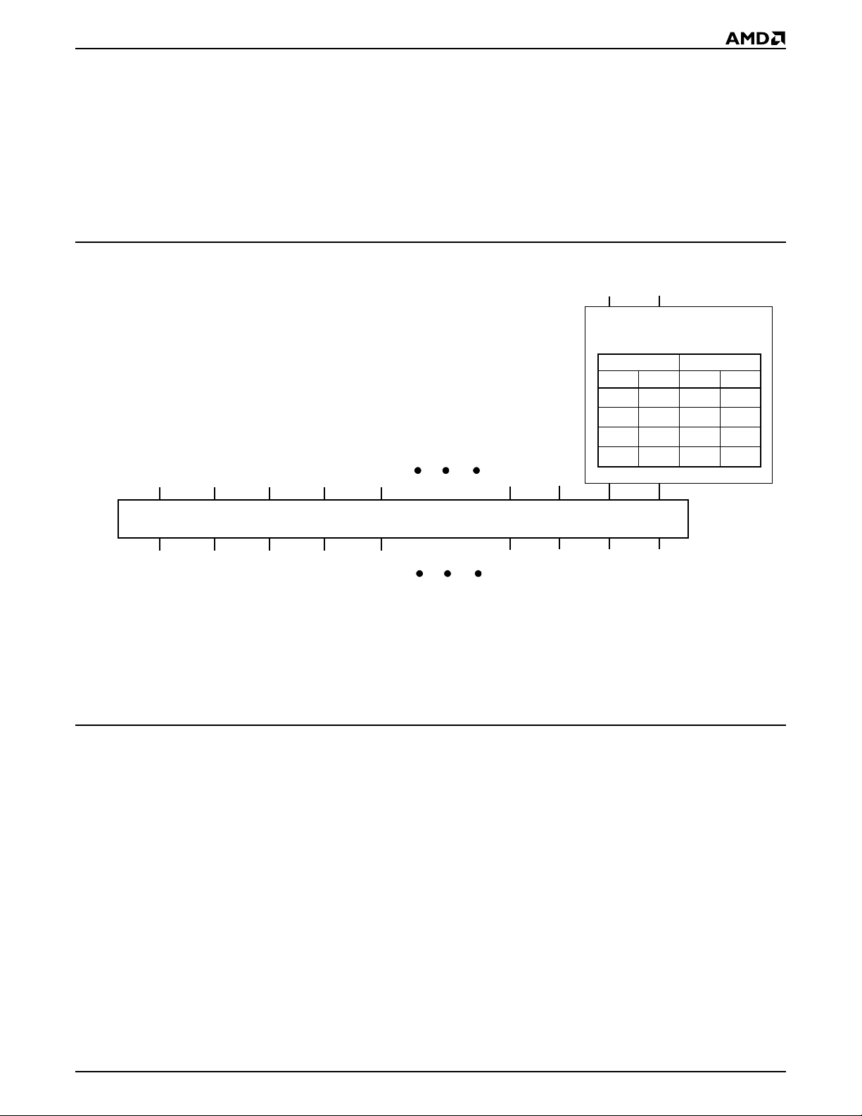
Figure 2 shows the connections betw een t he h ost and
Miniature Card. The host system address lines range
from A0–A25, whereas the Miniatur e Card address
Host Bus
A22
A21
A25
A24
A23
lines range f rom A0–A24. On the host, A0 and the
byte/word line are sent to a decoder and output to
CEL# and CEH# on the Miniature Card. These two bits
enable a single devi ce for byte accesses and two
devices for word accesses, as shown by the decoder
truth table in Figure 2. Again, the Miniature Card
address lines do not receive input from host address bit
A0. In this document, all address references are
addresses
, unless otherwise noted. T able 4 shows the
card
read/write modes for Miniature Cards.
Byte/Word
A0
Decoder
Decoder Truth Table
Input Output
A0 B/W CEL# CEH#
0000
0101
1000
A2
A1
1110
60-Pad Connector
A23*A24*
A22*
A21*
A20**
Card Bus
* Not connected
** Not connected on 2 Mbyte card
Figure 2. Host/Card Address Connections
Word-Wide Operations
The AMD Miniature Card provide the flexibility to
operate on data in a byte-wide or word-wide format. In
word-wide operations, the low bytes are controlled with
CEL#. The high bytes are controlled with CEH#. Refer to
the block diagram for more information.
Byte-Wide Operations
Byte-wide data is available for read and write operations (CEL# = 0, CEH# = 1). Even and odd bytes are
stored in separate memory devices (for example, S0
and S1) and are accessed by controlling CEL# and
CEH#. The even byte is the low order byte and the odd
byte is the high order byte of a 16-bit word.
Each memory sector or device pair must be addressed
separately for erase operations. Refer to the block
diagram for more information.
A1
CEH#CEL#A0
21138E-3
Card Detection
Each CD# (output) pin should be detected by the host
system to determine if the memory card is adequately
seated in the socket. CD# and CINS# are internally tied
to ground. If both bits are not d etected, the system
should indicate that the card must be re-inserted.
Data Protection
An optional mechanical write protect switch provides
user-initiated write protection. When this switch is acti-
WE# is internally forced high. The Flash memory
vated,
command register is disabled from accepting any write
commands. This prevents the card from responding to
any commands (for example, an Autoselect command). See Figure 3.
AmMCL00XA 9
Page 10

PRELIMINARY
Write Enabled
Write Disabled
Figure 3. Write Protect Switch
21138E-1
(Card Right Side View)
In addition to card-level data protection, AMD Flash
Miniature Cards offer several device-level data protection features.
Device-Level Data Protection
AMD Flash memory devices offer protection against
accidental erasure or programming caused by spurious
system level signals that may exist during pow er transitions. During power up, each device automatically
resets the internal state machine to the read mode. The
control register architectur e allows alteration of the
memory contents only occurs after successful completion of specific multi-bus cycle command sequences.
AMD Flash memory devices also incorporates the following features to prevent inadvertent write cycles
resulting from V
tions or system noise.
Low V
Write Inhibit
CC
To avoid initiation of a write cycle during V
and power-down, the AMD memory devices in the Miniature Card lock out write cycles for V
“DC Characteristics” on page 22 for voltages). When
< V
V
CC
LKO
internal program/erase circuits are disabled, and the
device resets to the read mode. The memory devices
ignore all write s until V
power-up and power-down transi-
CC
power-up
CC
CC
< V
LKO
(see
, the command register is disabled, all
CC
> V
. The user must
LKO
ensure that the control pins are in the correct logical
state when V
CC
> V
to prevent unintentional writes.
LKO
Write Pulse “Glitch” Protection
Noise pulses of less than 5 ns (typical) on OE#, CE# ,
or WE# will neither initiate a write cycle nor change the
command registers.
Logical Inhibit
Writing is inhibited by holding any one of OE# = V
CE# = V
, or WE# = VIH. To initiate a write cycle CE#
IH
IL
and WE# must be a lo gical ze ro whil e OE# is a logical
one.
Power-Up Write Inhibit
Power-up of the device with CE# = WE# = V
will not accept command s on the rising ed ge of
= V
IH
and OE#
IL
WE#. The internal state machine is automatically reset
to the read mode on power-up.
Read Mode
Two Card Enable (CE#) pin s are available on th e
memory card. Both CE # pins must be active low f or
word-wide read accesses. Only one CE# is required for
byte-wide accesses. The CE# pins select and determine when to appl y power to the high-byte and
low-byte memory devices. The Output Enable (OE#)
controls gating accessed data from the memory device
outputs. Refer to Table 4.
The Miniature Car d automatically power s up in the
read/reset state. In this case, a command sequence is
not required to read data. Standard microprocessor
read cycles will retrieve arra y data. This default state
ensures that no spurious alteration of the memory
content occurs during the power transition. Refer to the
AC Read Characteristics and Waveforms for the specific timing parameters.
Output Disable
Data outputs from th e card are di sabled when OE # is
at a logic-high level. Und er this conditio n, outputs are
in the high-impedance state.
,
10 AmMCL00XA
Page 11
PRELIMINARY
Table 4. Miniature Card Read/Write Modes
Function CEH# CEL# WE# OE# D8–D15 D0–D7
Read Mode
Word Access L L H L High Byte Data Low Byte Data
Low Byte Access H L H L High-Z Low Byte Data
High Byte Access L H H L High Byte Data Hi gh-Z
Write Mode
Word Access L L L H High Byte Data Low Byte Data
Low Byte Access H L L H High-Z Low Byte Data
High Byte Access L H L H High Byte Data Hi gh-Z
Standby Mode
Standby H H X X High-Z High-Z
Notes:
1. Unlisted access combinations are invalid and may return unexpected results.
2. X indicates a don’t care value.
Erase Operations
The AMD Flash Miniature Card is organized as an
array of individual devices. Each Am29LV081 device
contains sixteen 64 KByte sectors, for a total of 1 Mbyte
of memory space per device.
Flash technology allows any logical “1” data bit to be programmed to a log ica l “0 ”. T he on ly wa y t o r ese t bit s t o a
logical “1” is to erase that entire memory sector or
memory device. Once a memory s ector or memory
device is erased, any address location may be programmed. Two or more de vi ces m ay be er ase d co nc urrently when additional I
However, erasing more than two devices concurrently is
not typical in battery-powered applications, but may take
place during procedures such as card testing.
Erase operations can be performed in several ways:
■ Erase a single sector or multiple sectors in a device
■ Erase a sector pair
■ Erase multiple device pairs*
■ Erase the entire card*
* This operation is only feasible in solutions capable of
supplying more than the specified miniature card
supply current requirement (150mA) per system. Each
AMD Flash memory device pair can accept a
maximum of 120mA supply current.
The common memory space data contents are altered
in a similar ma nner to writing to individua l Flash
memory devices. An on-card address decoder activates the appropriate Flash device in the memory
current is supplied to the card.
CC
array. Each device internally latches address and data
during write cycles. Refer to Table 4.
Standby Mode
The AMD flash devices are designed to accommodate
low standby power consumption. In order to achieve
standby mode, the CE# line must be deselected. In
addition, while in the standby mode, data I/O pins
remain in the high impedance state independent of the
voltage level applied to the OE# input. See the DC
Characteristics section for more details on Standby
Modes.
Deselecting CE# (CE# and RE SET# = V
puts the device into the I
standby mode. If the
CC3
device is deselected during an Embedded Algorithm
operation, it continues to draw active power (I
to entering the standby mode, until the operation is
complete. When t he de vice is agai n selec ted (CE # =
), a c t i v e o p e r a t i on s occur in accordance with th e
V
IL
AC timing specifications.
Automatic Sleep Mode
Advanced power management features such as the
automatic sleep mode minimize Flash device energy
consumption. This is extremely important in battery-powered applications. The AMD memory devices
automatically enable the low-power, automatic sleep
mode when addresses remain stable for 300 ns. Automatic sleep mode is independent of the CE#, WE#, and
OE# control signals. Typical sleep mode current draw
from each device is < 1 µA. Standard address access
timings provide new data when addresses are
± 0.3 V)
CC
CC2
) prior
AmMCL00XA 11
Page 12

PRELIMINARY
changed. While in sleep mode, output data is latched
and always available to the system.
Command Definitions
Each memory device contains a command register,
which is a latch that saves address, commands, and
data information used by the state machine and
memory array. The state machine is active when V
greater than V
(2.3 - 2.5 V). This is required for valid
LKO
program and erase operations.
When Write Enable (WE#) and appropriate CE#
signals are at a logic-low level, and Output Enable
(OE#) is at a logic-high, the command register is
enabled for write ope rations. The fa lling edge of WE#
or CE#, whichever occurs later, latches address information and the rising e dge of W E# or CE# , which ever
occurs first, latches data/command information.
Commands are accomplished by writing non-specific
address and specific data sequences into the command register of accessed Flash memory devices.
Writing incorrect address and data values or writ-
CC
is
ing them in the improper sequence will reset the
device to the read mode.
The byte-wide comma nds are defined in Tables 6 and
7; word-wide com mands are defined i n Tab le 5. Note
that the Erase Suspend (B0h) and Erase Resume
(30h) commands are valid only while the Sector Erase
operation is in progress.
Autoselect Operation
A host system or external card reader/writer can determine the on-card manufacturer and device I.D. codes.
Codes are available after writing the 90h command to
the command register of a memory device, as shown in
Tables 5 throu gh 7. When the autoselect comman d is
issued to card address 00000h, the Miniature Card
returns the manufacturer I .D. If the autoselect
command is issued to card address 00001h, the Miniature Card provides the device I.D.
To term ina te th e autoselect operation, the Read/Reset
command sequence must be written to the same
device. The Autoselect command op erates only if the
card is not write protected.
12 AmMCL00XA
Page 13
PRELIMINARY
Table 5. Word Command Definitions
Bus Cycles (Notes 2–9)
Embedded Command
Sequence (Note 1)
Read 1 RA RW
Reset 1 XXXX F0F0
Autoselect Manufacturer ID
(Note 4)
Autoselect Device ID
(Note 4)
Word Write 4 XXXX AAAA XXXX 5555 XXXX A0A0 PA PW
Device Erase 6 XXXX AAAA XXXX 5555 XXXX 8080 XXXX AAAA XXXX 5555 XXXX 1010
Sector Erase 6 XXXX AAAA XXXX 5555 XXXX 8080 XXXX AAAA XXXX 5555 SA 3030
Sector Erase Suspend (Note 7) 1 XXXX B0B0
Sector Erase Resume (Note 8) 1 XXXX 3030
4 XXXX AAAA XXXX 5555 XXXX 9090 XX00 0101
4 XXXX AAAA XXXX 5555 XXXX 9090 XX01 3838
First Second Third Fourth Fifth Sixth
Cycles
Addr Data Addr Data Addr Data Addr Data Addr Data Addr Data
Legend:
X = Don’t care
RA = Address of the memory location to be read.
RW = Data read from location RA during read operation.
PA = Address of the memory location to be programmed.
PW = Data to be programmed at loc ation PA. Data is latched
on the rising edge of WE#.
SA = Address of th e secto r to be eras ed. Refer to Table 8 for
sector addresses.
Addresses are latched on the falling edge of the WE# pulse.
Notes:
1. Write protect must n ot be en abled for p roper op eration of
all commands. No command required for reading array
data, and can thus be done with write protect enabled.
2. During word addressing, CEL# = 0, CEH# = 0, and
address is applied to Memory De vice Pair 0 (S0 and S1).
On 4 Mbyte cards, address for Memory Device Pair 1 =
(Addr) + 200000h, and address is applied to Memory
Device Pair 1 (S2 and S3). For host-to-card address bit
connections, see Figure 2.
3. All values are in hexadecimal.
4. The last bus cycle in an autoselect command sequence is
a read operation.
5. Word = high byte + low byte.
6. Address bits = X = Don’t Care for all command s except for
Read Address (RA), Program Address (PA), and Sector
Address (SA).
7. The Erase Suspend command is valid only during a
sector erase operation . Refer to “Sector Eras e Suspen d”.
8. The Erase Resume command is valid only during the
Erase Suspend mode.
9. See Table 4 for bus operations.
AmMCL00XA 13
Page 14

PRELIMINARY
Table 6. E ven Byte Command Definitions
Bus Cycles (Notes 2–8)
Embedded Command Sequence
(Note 1)
Read 1 RA RD
Reset 1 XXXX XXF0
Autoselect Manufacturer ID (Note 4) 4
Device ID (Note 4) 4 XXXX XXAA XXXX XX55 XXXX XX90 XX01 XX38
Byte Write 4 XXXX XXAA XXXX XX55 XXXX XXA0 PA PD
Device Erase 6
Sector Erase 6
Sector Eras e Su s pe n d ( N ot e 6) 1 XXXX XXB0
Sector Erase Resume (Note 7) 1 XXXX XX30
First Second Third Fourth Fifth Sixth
CyclesCycles
Addr Data Addr Data Addr Data Addr Data Addr Data Addr Data
XXXX XXAA XXXX XX55 XXXX XX90 XX00 XX01
XXXX XXAA XXXX XX55 XXXX XX80 XXXX XXAA XXXX XX5 5 XXXX XX10
XXXX XXAA XXXX XX55 XXXX XX80 XXXX XXAA XXXX XX55 SA XX30
Note for Table 6: During even (low) byte accesses, CEL# = 0, CEH# = 1. Address is applied to Memo ry Device 0 (S0). On 4 Mbyte
cards, address for Memory Device 2 (S2) = (Addr) + 20000 0h.
Table 7. Odd Byte Command Definitions
Bus Cycles (Notes 2–8)
Embedded Command Sequence
(Note 1)
Read 1 RA RD
Reset 1 XXXX XXF0
Autoselect Manufacturer ID (Note 4) 4
Autoselect Device ID (Note 4) 4 XXXX AAXX XXXX 55XX XXXX 90XX XX01 38XX
Byte Write 4 XXXX AAXX XXXX 55XX XXXX A0XX PA PDXX
Device Erase 6
Sector Erase 6
Sector Eras e Su s pe n d ( N ot e 6) 1 XXXX XXB0
Sector Erase Resume (Note 7) 1 XXXX XX30
First Second Third Fourth Fifth Sixth
Addr Data Addr Data Addr Data Addr Data Addr Data Addr Data
XXXX AAXX XXXX 55XX XXXX 90XX XX00 01XX
XXXX AAXX XXXX 55XX XXXX 80XX XXXX AAXX XXXX 55XX XXX X 10XX
XXXX AAXX XXXX 55XX XXXX 80XX XXXX AAXX XXXX 55XX SA 30XX
Note for Table 7: During odd (high) byte accesses, CEL#= 1, CEH# = 0, and address is applied to Memory Device 1 (S1). On 4 Mbyte
cards, address for Memory Device 3 (S3) = (Addr) + 20000 0h + 1000 00h .
Legend for Tables 6 and 7:
X = Don’t care
RA = Address of the memory location to be read.
RW = Data read from location RA during rea d opera tion .
PA = Address of the memory location to be programmed.
PW = Data to be programmed at location PA. Data is latched on
the rising edge of WE#.
SA = Address of the sector to be eras ed. Refer to Table 8 for
sector addresses.
Addresses are latche d on the falling edge of the WE# pulse.
Notes for Tables 6 and 7:
1. Write protect must not be enabled for proper operation of all
commands. No comm a nd r equ ired for read in g ar ra y data ,
and can thus be done with write prote ct ena bled.
2. For host- to-card addres s bit c onn ect i ons, see Figur e 2.
3. All values are in hexadecim al.
6. The Erase Suspend com man d is va lid only dur ing a sect or
erase operation. Refe r to “S ect or Erase Susp en d” .
7. The Erase Resume command is valid only during the Erase
Suspend mode.
8. See Table 4 for bus operat io n s .
4. The last bus cycle in an autoselect command sequence is a
read oper at ion.
5. Address bits = X = Don’t Care for al l comm an ds ex ce pt for
Read Address (R A) , Progr am A d dr es s (PA), and Sector
Address (SA).
14 AmMCL00XA
Page 15

PRELIMINARY
Table 8. Memory Sector Addresses
Card Address Bits Device 0 and/or 1 (Note 1) Device 2 and/or 3 (Note 1)
Sector
0 0 0 0 0 00000h–0FFFFh 100000h–10FFFFh
1 0 0 0 1 10000h–1FFFFh 110000h–11FFFFh
2 0 0 1 0 20000h–2FFFFh 120000h–12FFFFh
3 0 0 1 1 30000h–3FFFFh 130000h–13FFFFh
4 0 1 0 0 40000h–4FFFFh 140000h–14FFFFh
5 0 1 0 1 50000h–5FFFFh 150000h–15FFFFh
6 0 1 1 0 60000h–6FFFFh 160000h–16FFFFh
7 0 1 1 1 70000h–7FFFFh 170000h–17FFFFh
8 1 0 0 0 80000h–8FFFFh 180000h–18FFFFh
9 1 0 0 1 90000h–9FFFFh 190000h–19FFFFh
10 1 0 1 0 A0000h–AFFFFh 1A0000h–1AFFFFh
11 1 0 1 1 B0000h–BFFFFh 1B0000h–1BFFFFh
12 1 1 0 0 C0000h–CFFFFh 1C0000h–1CFFFFh
13 1 1 0 1 D0000h–DFFFFh 1D0000h–1DFFFFh
14 1 1 1 0 E0000h–EFFFFh 1E0000h–1EFFFFh
15 1 1 1 1 F0000h–FFFFFh 1F0000h–1FFFFFh
A19 A18 A17 A16 Card Address Range Card Address Range
Notes:
1. For word addressing, devices 0 and 1 (S0 and S1) together form Memory Device Pair 0; devices 2 and 3 (S2 and S3) form
Memory Device Pair 1. Refer to the block diagram for device connections.
2. Card address bits range from A0 to A19. Host ad dress bits rang e from A0 to A20. Hos t address bit A0 is used for co ntrolli ng
the CEL# and CEH# inputs to the card. Refer to Figure 2 for host-to-card address bit connections.
AmMCL00XA 15
Page 16

PRELIMINARY
AMD FLASH MEMORY PROGRAM AND
ERASE OPERATIONS
To simplify prog ram a nd erase ope ratio ns, AMD Fla sh
Memory devices include Embedded Algorithms
(Embedded Erase Algorithm and Embedded Program
Algorithm) that allow the host to simply issue a command, after which it is free to perform other tasks. The
host then only needs to monitor appropriate status bits
to determine when the operation is complete.
Embedded Erase Algorithm
When erasing a sector or device, the Embedded Erase
algorithm does not require the host to first entirely
pre-program the device. Upon executing the
Embedded Erase comman d seq uence , the addr essed
memory sector or memory device automa tically wri tes
and verifies the entire memory device or memory
sector for an all “0” data pattern. The system is not
required to provide any controls or ti mi ng during these
operations.
When the memory sector or memory dev ice is automatically verified to contain an all “0” pattern, a
self-timed chip erase-and-verify begins. The erase and
verify operations are complete when the data on D7
(D15 on the odd byte) of the memory sector or memory
device is “1” (see Write Operation Status section), at
which time the device returns to the read mode. The
system is not required to provide any control or timing
during these operations. If a Reset command is issued
while the erase operation is in progress, the erase
operation will stop, and the data in that device will be
undefined. In that case, restart the erase on that sector
and allow it to complete.
When using the Embedded Erase algorithm, the erase
automatically terminates when adequate erase margin
has been achieved for the memory array (no erase
verify command is required).
The Embedded Erase command sequence is a
command only operation that stages the memory
sector or memo ry device for automatic electrical
erasure of all bytes in the array. The automatic erase
begins on the rising edge of the
when the data on D7 (D15 on the odd byte) of the
memory sector or memory device is “1” (see Write
Operation Status section) at which time the device
returns to the Read mode. Please no te that for the
memory device or memory sector erase operation,
Data Polling may be performed at any address in that
device or sector.
Figure 4 and Table 9 illustrate the Embedded Eras e
Algorithm, a typical command string and bus operations.
As described earlier, once the memory sector in a
device or memory device completes the Embedded
Erase operatio n, it returns to the Read mo de and
addresses are no longer latched. Therefore, the device
WE# and terminates
requires that a valid address input to the device is
supplied by the system at this particular instant of time.
Otherwise, the system will never read a “1” on D7 (D15
on the odd byte). A system designer has the follo wing
choices to impleme nt the Embedded Era se algorithm :
1. The host may keep the sector address (with in any
of the sectors being erased) valid during the entire
Embedded Erase operation.
2. Once the system executes the Embedded Erase
command sequence, the h ost may remove t he address from the device and perform other tasks. The
host is required to keep track of the valid sector address by loading it into a temporary regi ster. When
the host comes back to Data Poll the device, it must
reassert the same address.
3. The host may monitor BUSY# (RY/BY#) to determine the status of the Embedded Algorithm in
progress. A “0” indicates that the d evice is busy; a
“1” indicates that the algorithm is complete.
Sector Erase
Sector erase is a six bus cycle operation. There are two
“unlock” write cycles. These are followed by writing the
“set-up” command. Two more “unlock” write cycles are
then followed by the sector erase command. The
sector address (any address location within the desired
sector) is latched on the falling e dge of WE# (or CE #),
whichever occurs later, while the data is latched on the
rising edge of WE# (or CE#) pulse, whichever occurs
first. A time-out of 80 µs from the rising edge of the last
sector erase command will initiate the sector erase
command.
Multiple sectors can be specified for erase by writing
the six bus cycle operation as described above and
then following it by additional writes of the Sector Erase
command to addresses of ot her sectors to be erased.
The time between Sector Erase command writes must
be less than 80 µs, otherwise that command will not be
accepted. It is recommended th at processor int errupts
be disabled during this time to guarantee this condition.
The interrupts can be re-enabled after the last Sector
Erase command is written. A time-out of 80 µs from the
rising edge of the last WE# (or CE#) will initiate the execution of the Sector Erase command(s). If another
falling edge of the WE# (or CE #) occurs within the 80
µs time-out window, the timer is reset. During the 80 µs
window, any command other than Sector Erase or
Erase Suspend written to the de vice will reset the de vice back to Read mode. Once the 80 µs w indow has
timed out, only t he E ra se s usp end co mm and is r e cognized. Note that although the Reset command is not
recognized in the Erase Suspend mo de, the device is
available for read or program operations in sectors that
are not erase suspended. The Erase Suspende d and
Erase Resume commands may be writt en as often as
required during a sector erase operation. Hen ce , once
erase has begun, i t must ultimately c omplete unless
16 AmMCL00XA
Page 17

PRELIMINARY
Hardware Reset is initiated. Loading th e sector erase
registers may be done in any sequence and wi th any
number of sectors (0 to 15).
A Reset command issued after the device ha s begun
execution stops the erase operation, but the data in the
sector will be undefined. In that case, restart the erase
on that sector and allow it to complete.
The automatic sector erase begins after the 80 µs time
out from the rising edge of th e
WE# (or CE#) pulse for
the last sector erase command pulse and terminates
when the data on D7 is “1” (see Write Operation Status
section) at which time the device returns to read mode.
Data Polling must be performed at an address within
any of the sectors being erased.
If DATA Polling or the Toggle Bit indicates the device
has been written with a valid Sector Erase command ,
D3 may be used to determi ne if the sect or erase tim er
window is still open. If D3 is high (‘1’), the internally
controlled erase cycle has begun; attempts to write
subsequent commands to the d evice will be ignored
until the erase operation is co mpleted as indi cated by
the DATA Polling or Toggl e Bit. If D3 is low (‘0’), the
device will accept additional sector erase comman ds.
To be certain the c ommand has bee n accepted, t he
software should check th e status of D3 fol lowin g each
Sector Erase command. If D3 was hig h on the second
status check, the c ommand may not have been
accepted.
It is recomm ended that th e user guaran tee the time
between sector erase command writes be less than 80
µs by disabling the processor interrupts just for the
duration of the Sector Erase (30H) commands. This
approach will ensure that sequential sector erase
command writes will be written to the device whi le the
sector erase timer window is still open.
Figure 4 illustrates the Embedded Erase Algori thm
using typical command strings and bus operations.
Table 9. Embedded Erase Algorithm
Bus
Operation Command Com ments
Standby Wait for V
Write
Read
Embedded Erase
command sequence
6 bus cycle operation
Data Poll or check
BUSY# (RY/BY#)
to verify erasure
CC
ramp
Start
Write Embedded Erase
Command Sequence
(See Tables 5–7)
Data Poll from Device
or wait for BUSY#
(RY/BY#)
Erasure Complete
21138E-5
Figure 4. Embedded Erase Algorithm
Note: The latest release of the software drivers for AMD
Miniature Cards and devices may be downloaded from the
AMD web site at http://www.amd.com.
Embedded Program Algorithm
The Embedded Program setup is a four bus cycle operation that stages the addressed memory location or
memory device for automatic programming.
Once the Embedded Program setup ope ration is performed, the next
active programming operation. Addresses are internally latched on the falling edge of the
pulse. Data i s internally la tched on the rising edge o f
WE# pulse. The rising edge of WE# also begins the
the
programming operation. The system is not required to
provide further control or timing. The d evice will automatically pro vide an adequate internally genera ted
write pulse and verify margin. The autom ati c prog ramming operation is completed when the data on D7 of
the addressed memory secto r or memory device is
equivalent to data written to this bi t (see Write Operation Status section) at which time the device returns to
the Read mode (no write verify command is required).
Addresses are latched on the falling edge of
CE#) during the Embedded Program command execu-
tion and hence the system is not required to keep the
addresses stable during the entire Programming operation. However, once the device completes the
Embedded Program operation, it returns to the Read
mode and addresse s are no longer latched. Since a
verify valid d ata must occur on D7, at this particu lar
instant, the system is requ ired to sup pl y a valid ad dress
input to the device. A system designer has th ree choices
to implement the Embed de d Pro g ram min g a lgor ith m:
WE# pulse causes a transition to an
WE# (or CE#)
WE# (or
AmMCL00XA 17
Page 18

PRELIMINARY
1. The system (CPU) keeps the address valid during
the entire Embedded Programmin g operati on, or
2. Once the system execu tes the Embedded Programming command sequence, the CPU takes
away the address from the device and becomes
free to do other tasks. In this case, the CPU is required to keep track of the valid address by loading
it into a temporary register. When the CPU comes
back for performing Data Polling, it shou ld reassert
the same address.
3. The host may monitor BUSY# (RY/BY#) to determine the status of the Embedded Algorithm in
progress. A “0” indicates that the device i s busy; a
“1” indicates that the algorithm is complete.
However, since the Embedded Programming operation
takes only 9 µs typically, it may be easier for the CPU
to keep the address stable during the entire Embedded
Programming operation instead of reasserting the valid
address during Data Polling. Any commands written to
the device during this peri od will be ignored. Figure 5
and Table 10 illustrate the Embedded Program Algorithm, a typical command string, and bus operation.
Increment
Address
Start
Write Embedded Write Command
Sequence per Tables 5–7
Data Poll Device
or wait for BUSY# (RY/BY#)
N
Y
Y
N
Verify
Data
Last
Address
Completed
Table 10. Embedded Program Algorithm
Bus
Operation Command Comments
Standby Wait for V
Write
Write
Read
Embedded Program
command sequence
Program
Address/Data
3 bus cycle operation
1 bus cycle operation
Data Poll or check
BUSY# (RY/BY#) to
verify program
CC
ramp
21138E-6
Figure 5. Embedded Program Algorithm
Reset Command
The device will autom atically po wer up in the rea d/reset state. In this case, a command sequence is not required to read data. Standard microprocessor cycles
will retrieve array data. This default value ensures that
no spurious alteration of the memory content occurs
during the power transition. Refer to the AC Characteristics section for the specific timing parameters.
The reset operation is initiated by writing the read/reset
command sequence into the command register. Microprocessor read cycles retrieve array data from the
memory. The device remains enabled for reads until
the command register contents are altered.
Sector Erase Suspend
The Erase Suspend command allows the user to interrupt a Sector Erase operation and then perform data
read or programs in a sector not being e rased. This
command is applicable only during the Sector Erase
operation, which includes the time-out period for Sector
Erase. The Erase Suspend command will be ignored if
written during the exe cution of the Chip E rase operation or Embedded Program Algorithm (but will reset the
chip if written improperly dur ing the command sequences.) Writing the Erase Suspend command during
the Sector Erase time-out results in immediate termination of the time-out period and suspension of the erase
operation. Once in Erase Suspend, the device is avail-
18 AmMCL00XA
Page 19

PRELIMINARY
able for read (note that in the Erase Suspend mode, the
Reset/Read command is no t required for read ope rations and is ignored) or pro gram operatio ns in sectors
not being erased. Any other command written during
the Erase Suspend mode will be ignored, except for the
Erase Resume comman d. Writing the Erase Re sume
command resumes the sector erase operation. The addresses are “don’t cares” when writing the Erase Suspend or Erase Resume command.
When the Erase Suspend command is written during a
Sector Erase operati on, the chip wi ll take between 0.1
µs and 20 µs to actually suspend the operation and go
into erase suspended read mode (pseudo-read mode),
at which time the user can read or program from a sector that is not erase suspended. Re ading data in this
mode is the s ame as readi ng from th e standard re ad
mode, except that the data must be read from sectors
that have not been erase suspended.
Successively reading from the erase-suspended sector while the device is in the erase-suspend-read mode
will cause D2 to toggle. Polling D2 on successive reads
from a given sector provides t he system the ability to
determine if a sector is in Erase Suspend.
After entering the erase-suspend -read mode , the user
can program the device by writing the appropriate command sequence for Byte Program. This program mode
is known as the erase suspend-program mode. Again,
programming in this mode is the same as programming
in the regular Byte Program mode, except that the data
must be programmed to sectors that are not erase suspended. Successively reading from the erase suspended sector while the device is in the erase
suspend-program mode wi ll cause D 2 to tog gle . Completion of the erase suspend operation can be determined two ways:
■ Checking the status of the toggle bit D2
■ Checking the status of the RY/BY# pin
To resume t he o perat ion of Secto r Erase, the Resume
command (30H) should be written. Any further writes of
the Resume command at this point will be ignored.
However, another Erase Susp end command can be
written after the device has resumed sector erase operations.
Write Operation Status
Table 11 shows the status bit states for device program
and erase operations.
ded Program Algorithm, an attem pt to rea d th e device
will produce the true data last writ ten to D7. Note that
just at the instant w hen D7 switches to true d ata, the
other bits, D6–D0, may not yet b e true data . H owever,
they will all be true data on the next read from the device. Please note that Data Polling (D7) may give an
inaccurate result when an attempt is made to write
to a protected sector. During an Embedded Erase Al-
gorithm, an attempt to read the device will produce a ‘0’
at the D7 output. Upon completion of the Embedded
Erase Algorithm, an attempt to read
the device will produce a ‘1’ at D7.
START
DQ7 = Data?
No
No
Note: D7 is rechecked even if D5 = 1 because D7 may
change simulta neo us ly with D5.
DQ5 = 1?
Yes
DQ7 = Data?
No
FAIL PASS
Yes
Yes
21138E-7
Figure 6. Data Polling Algorithm
Data Polling—D7 (D15 on Odd Byte)
The Miniature card features DATA Polling as a method
to indicate to the host system that the embedded algorithms are in progress or completed.
During the Embedded P rogram Algorithm , an attempt
to read the device wil l produce the compliment o f the
data last written to D7. Upon completion of the Embed-
AmMCL00XA 19
Page 20

PRELIMINARY
Table 11. Hardware Sequence Flags
Status D7 D6 D5 D3 D2
Byte Program in Embedded Program Algorithm D7 Toggle 0 0 1
Embedded Erase Algorithm 0 Toggle 0 1 Toggle
Erase Suspend Read
In Progress
Erase Suspended Mode
Byte Program in Embedded Program Algorithm D7 Toggle 1 0 1
Exceeded
Time Limits
Notes:
1. Performing successive read operations from the erase-suspended sector will cause D2 to toggle.
2. Performing successive read operations from any address will cause D6 to toggle.
3. Reading the byte address being programmed while in the erase-suspend program mode will indicate logic “1” at the D2 bit.
However, successive reads from the erase-suspended sector will cause D2 to toggle.
Program/Erase in Embedded Erase Algorithm 0 Toggle 1 1 N/A
Erase Suspended Mode
BUSY# (RY/BY#—Ready/Busy)
The BUSY# signal indicates to the host the status of
operations with in the Miniature Card. Th e BUSY#
signal is tied to the components’ RY/BY# pins.
The RY/BY# signal from AMD Flash devices in
the Miniature Card indicate that the Emb ed de d Algo rithms are eit her in pro gress or have been co mpleted.
If the output is low, the device is busy with either a
program or erase operation. If the output is high, the
device is ready to accept any read/write or erase operation. When the RY/BY# pin is low, the device will
not accept any additi onal program or erase commands with the ex ception o f the Er ase Suspen d command. If a Flash device is placed in an Erase
Suspend mode, the R Y/BY# output will be high. Refer
to the section “Se cto r Er a se Susp end” fo r mo re i nf ormation.
(Erase Suspended Sector)
Erase Suspend Read
(Non-Erase Suspended Sector)
Erase Suspend Program
(Non-Erase Suspended Sector)
Erase Suspend Program
(Non-Erase Suspended Sector)
WORD-WIDE PROGRAMMING
The Word-Wide Programming sequence will be as
usual per Table 5. The Program word command is
A0A0H. Each byte is inde pendently pro grammed. For
example, if the high byte of the word indicates
the successfu l completion of programming via one of
its write status bits such as D15, software polling
should con tinue to monitor the low byte for write co mpletion and data verifica tion, or vice versa. During the
Embedded Programming operations the device executes programming pulses in 9 µs increments.
WORD-WIDE SECTOR ERASING
The Word-Wide Sector Erasing of a memory device
pair is similar to word-wide programming. The erase
word command is a six-bus-cycle command sequence
(see T able 5). Each sector is independently erased and
1100
Data Data Data Data Data
D7
D7 Toggle 1 1 N/A
Toggle
(Note 2)
01
Toggle
(Note 1)
1
(Note 3)
verified. Word-wide erasure reduces total erase time
when compared to byte erasure. Each Flash memory
device in the card may erase at different rates. Therefore, each device (byte) must be verified separately.
20 AmMCL00XA
Page 21

PRELIMINARY
ABSOLUTE MAXIMUM RATINGS
Storage Temperature . . . . . . . . . . . . . –40°C to +90°C
Ambient Temperature
with Power Applied . . . . . . . . . . . . . . –40°C to +85°C
Vo ltage at All Pins (Note 1) . . . . –0.5 V to V
V
(Note 1) . . . . . . . . . . . . . . . . . . . .–0.5 V to 3.6 V
CC
Output Short Circuit Current (Note 2) . . . . . . 200 mA
Notes:
1. Minimum DC voltage on input or I/O pin s is –0.5 V . During
voltage transitions, inputs may overshoot V
for periods of up to 20 ns. Max imum DC voltage on output
and I/O pins is VCC + 0.5 V. During voltage transitions,
outputs may overshoot to V
20ns.
2. No more than one output shorted at a time. Duration of
the short circuit should not be greater than one second.
Conditions equal V
These values are chosen to avoid test problems caused
= 0.5 V or 3.6 V, VCC = V
OUT
+ 2.0 V for periods up to
CC
CC
to –2.0 V
SS
+0.5 V
CCmax
.
by tester ground d egrada tion. Th is paramete r is sample d
and not 100% tested , but guarante ed by charac terization.
3. Stresses above those listed under “Absolute Maximum
Ratings” may cause perman ent damage to the devi ce.
This is a stre ss ra ting on ly; fu nct ion al ope ration of th e device at these or any other condit ion s abo ve those indicated in the operational sections of this specification is
not implied. Exposu re of the device to absolute maximu m
rating conditions for extended periods may affect device
reliability.
OPERATING RANGES
Commercial Devices
Case Temperature (T
Industrial (I) Devices
Case Temperature (T
V
Supply Voltages
CC
AmMCL00XAWP-150 . . . . . . . . . . . . +2.7 V to +3.6 V
Operating ranges define those limi ts betwe en whic h the
functionality of the device is gua ranteed.
). . . . . . . . . . . . . .0°C to +70°C
C
). . . . . . . . . . . .–40°C to +85°C
C
AmMCL00XA 21
Page 22

PRELIMINARY
DC CHARACTERISTICS
Parameter
Symbol Parameter Description Test Conditions Min Max Unit
I
V
Notes:
1. V
I
I
LO
CCS
I
CC
V
V
V
V
LKO
CC
LI
IL
IH
OL
OH
Input Leakage Current VIN = VSS to V
Output Leakage Current VIN = VSS to V
CEL#, CEH#, RESET# = VCC ± 0.3
VCC Standby Current
VCC Supply Current, word
mode (Note 2)
V
= 3.6V; VIN = VSS or V
V
CC
RESET# = VIH; CEL# and CEH# =
V
IL
CC, VCC
CC, VCC
= V
= V
CC max
CC max
CC
2 Mbyte 30 µA
4 Mbyte 40 µA
Read 40 mA
Write 60 mA
Input Low Voltage –0.5 0.8 V
Input High Voltage 0.7 V
Output Low Voltage I
Output High Voltage I
= 5.8 mA 0.45 V
OUT
= –2.0 mA 0.85 V
OUT
CCVCC
CC
Low VCC Lock-Out Voltage 2.3 2.5 V
2. Supply current is a max RMS value. Read frequ ency = 5
= 2.7 V to 3.6 V.
MHz.
±5 µA
±5 µA
+ 0.5 V
CONNECTOR DC SPECIFICATIONS
Parameter Min Max Units
Interface Signal Resistance (Note 2) 2.0 Ω
V
Interface Signal Current (Notes 1, 2) 125 mA
Power/Insertion Signal Resistance 0.060 Ω
Power/Insertion Signal Current (Note 1) 500 mA
Notes:
1. This current is a minimum that the connector should withstand, and a maximum that the host should provide.
2. On the host, these specifications must be met for one conducting channel on elastomeric connectors.
CARD AND PAD CAPACITANCE
Parameter Symbol Parameter Description Test Conditions Max Unit
C
CARD
C
HOST
C
I/O Capacitance D0-D15 40 pF
I/O
Notes:
1. Sampled, not 100% tested.
2. Test conditions TA = 25°C, f = 1.0 MHz.
Card Input Capacitance 40 pF
System Load Capacitance 120 pF
22 AmMCL00XA
Page 23

AC CHARACTERISTICS
Read-only Operations
Parameter Symbol
Parameter Description -150 UnitJEDEC Standard
PRELIMINARY
t
AVAV
t
ELQV
t
AVQV
t
GLQV
t
ELQX
t
EHQZ
t
GLQX
t
GHQZ
t
AXQX
t
RC
t
CE
t
ACC
t
OE
t
LZ
t
DF
t
OLZ
t
DF
t
OH
t
Ready
Read Cycle Time Min
150
ns
Chip Enable Access Time Max 150 ns
Address Access Time Max 150 ns
Output Enable Access Time Max 50 ns
Chip Enable to Output in Low-Z Min 5 ns
Chip Disable to Output in High-Z Max 30 ns
Output Enable to Output in Low-Z Min 5 ns
Output Disable to Output in High-Z Max 30 ns
Output Hold from First of Address, CE#, or OE# Change Min 5 ns
RESET# Pin Low to Read Mode Max 20 µs
AmMCL00XA 23
Page 24

AC CHARACTERISTICS
Write Operations (Erase/Program)
Parameter Symbols
Parameter Description -150 UnitJEDEC Standard
PRELIMINARY
t
AVAV
t
WLWH
t
ELGL
t
ELWL
t
AVGL
t
AVWL
t
DVWH
t
WHDX
t
WHAX
t
WHEH
t
WHWH1
t
WHWH2
t
WC
t
RP
t
BUSY
Write Cycle Time Min 150 ns
WE# pulse width Min 50 ns
CE# setup time to WE# or OE# active Min 0 ns
Address setup time to WE# or OE# active Min 0 ns
Data setup time to WE# inactive Min 50 ns
Data hold time from WE# inactive Min 0 ns
Address hold time from WE# inactive Min 0 ns
CE# hold time from WE# inactive Min 0 n s
RESET# Pulse Width Min 500 ns
Program/Erase Valid to RY/BY# Delay Min 90 ns
Typ 9
Programming Operation
Max 300 µs
Typ 1.5
Sector Erase Operation
Max 15 s
24 AmMCL00XA
Page 25

KEY TO SWITCHING WAVEFORMS
WAVEFORM INPUTS OUTPUTS
PRELIMINARY
SWITCHING WAVEFORMS
Must be
Steady
May
Change
from H to L
May
Change
from L to H
Don’t Care,
Any Change
Permitted
Does Not
Apply
Will be
Steady
Will be
Changing
from H to L
Will be
Changing
from L to H
Changing,
State
Unknown
Center
Line is HighImpedance
“Off” State
KS000010
A0–A25
CEL#/CEH#
OE#
D0–D15
t
AVGL
t
ELGL
t
ELQNZ
t
AVQV
t
t
GLQNZ
ELQV
t
AVAV
t
GLQV
Valid Data
t
AXQX
t
EHQX
t
GHQZ
t
GHQX
Figure 7. AC Waveforms for Read Operations
AmMCL00XA 25
21138E-8
Page 26

SWITCHING W AVEFORMS
PRELIMINARY
A0–A25
CEL#/CEH#
WE#
D0–D15
t
AVAV
t
AVWL
t
ELWL
t
WLWH
t
DVWH
t
Valid Data
Figure 8. AC Waveforms for Write Operations
t
WHAX
t
WHEH
WHDX
21138E-9
t
CE#
OE#
WE#
D7
D0–D6
CH
t
OEH
t
OE
t
CE
t
WHWH1 or tWHWH2
D7#
D0–D6=Invalid
*D7=Valid Data (The device has completed the Embedded operation).
*
t
OH
D7=
Valid Data
D0–D7
Valid Data
t
DF
High Z
21138E-10
Figure 9. AC Waveforms for Data Polling During Embedded Algorithm Operations
26 AmMCL00XA
Page 27

SWITCHING W AVEFORMS
CE#
PRELIMINARY
The rising edge of the last WE# signal
WE#
Entire programming
or erase operations
RY/BY#
t
BUSY
Figure 10. RY/BY# Timing Diagram During Program/Erase Operations
RESET#
t
RP
t
Ready
Figure 11. RESET# Timing Diagram
21138E-11
21138E-12
AmMCL00XA 27
Page 28

PRELIMINARY
AC CHARACTERISTICS-ALTERNATE CE# CONTROLLED WRITES
Write/Erase/Program Operations
Parameter Symbols
Parameter Description -150 UnitJEDEC Standard
t
AVAV
t
AVEL
t
ELAX
t
DVEH
t
EHDX
t
GLDV
t
GHEL
t
WLEL
t
EHWH
t
ELEH
t
EHEL
t
EHEH3
t
EHEH4
t
VCS
t
WC
t
AS
t
AH
t
DS
t
DH
t
OEH
t
WS
t
WH
t
CP
t
CPH
Write Cycle Time Min 150 ns
Address Setup Time Min 10 ns
Address Hold Time Min 50 ns
Data Setup Time Min 50 ns
Data Hold Time Min 0 ns
Output Enable Hold Time for Embedded Algorithm Min 10 ns
Read Recovery Time before Write Min 0 µs
WE# Setup Time before CE# Min 0 ns
WE# Hold Time Min 0 ns
CE# Pulse Width Min 50 ns
CE# Pulse Width HIGH (Note 3) Min 20 ns
Embedded Programming Operation (Notes 3,4)
Embedded Erase Operati on for each 64K byte Memo ry
Sector (Notes 1, 2)
VCC Setup Time to Write Enable LOW Min 50 µs
Typ 9
Max 300 µs
Typ 1.5
Max 15 s
Notes:
≤
1. Rise/fall time
10 ns.
2. Maximum specification not needed due to the internal stop timer that will stop any erase or write operation that exceed the
device specification.
3. Card Enable Controlled Programming:
Flash Programming is controlled by the valid combination of the Card Enable (CE1#, CE2#) and Write Enable (WE#) signals.
For systems that use the Card Enable sign al(s) to define the wri te pulse width, all setup, hold, and in active write enab le timing
should be measured relative to the Card Enable signal(s).
°
4. Under worst case condition of 90
C, Vcc = 2.7 V , 100 ,000 cycles. Excludes sy ste m level overhead, the time require d to
execute the four bus cycle command necessary to program each byte.
28 AmMCL00XA
Page 29

PRELIMINARY
Addresses
t
WC
XXXXh
t
AS
PA PA
t
AH
WE#
t
WH
OE#
t
GHEL
t
CE#
Data
V
CC
t
VCS
t
WS
A0h
CP
t
CPH
t
DS
t
DH
PD
t
Notes:
1. PA is address of the memory location to be programmed.
2. PD is data to be programmed at byte address.
3. D7 is the complement of the data written to the device.
4. D
is the data written to the device.
OUT
5. Figure indicates last two bus cy cl es of four bus cyc le seq ue nce.
6. These waveforms are for the x16 mode.
Figure 12. Alternate CE# Controlled Write Operation Timings
Data# Polling
EHEH3_or_4
DQ7# D
OUT
21138E-13
AIS MEMORY MAP
The AIS (Attribute Information Structure) is an area of
memory used for storing informa tion a bout the co nfiguration of the Miniature Card. The AIS is recommended
to be stored in the first sector of the first device of the
Flash array. As this area is not explicitly protected , the
AIS information must b e reloaded o nto the card in the
event that the information is erased.
The AIS has five unique information areas:
1. Identification Data: This data includes Manufacturer
information (Manufacturer and card name).
2. Compatibility Data: This data spe cifies basic information about the card (memo ry size, access time,
memory type, power, etc.)
3. Burst Data (not applicable)
4. DRAM Data (not applicable)
5. Reserved Data: This data area is reserved for future use.
AmMCL00XA 29
The AIS supports up to four different memory technologies on a card. Some of the information areas are
repeated in the memory map in order to specify different technologies (see Table 12). The Technology
Count field in the Identification Data section defines the
number of different technologies on a card. The first
memory technology is defined in the AIS memory map
from address 40H through 7FH. The second memory
technology is defined from 80H through BFH. The third
memory technology is d efined from C0 H to DFH. Th e
fourth memory technology is defined from E0H to FFH.
The AIS is stored as bytes within the 16-bit Miniature
Card data word. The even byte D0–D 7 stores the AIS
data, and the odd byte D8–D15 is reserved by the card
manufacturer for manufact uring informa tion.
Page 30

PRELIMINARY
Table 12. Miniature Card AIS Memory Assignments
Card Address Sectio n Description
00h–0Fh PC Card Compatibility Area* Reserved for PC Card Tuples
10h–1Fh Identification Data Identifies Card Type
20h–2Fh Identification Data Identifies Card Type
30h–3Fh Identification Data Identifies Card Type
40h–4Fh Compatibility Data (Area 1) Memory Technology #1
50h–5Fh Burst Data (not applicable)
60h–6Fh DRAM Data (not applicable)
70h–7Fh Reserved for future use
80h–8Fh Compatibility Data (not applicable) (Memory Technology #2)
90h–9Fh Burst Data (not applicable)
A0h–AFh DRAM Data (not applicable)
B0h–BFh Reserved for future use
C0h–CFh Compatibility Data (not applicable) (Memory Technology #3)
D0h–DFh Reserved for future use
E0h–EFh Compatibility Data (not applicable) (Memory Technology #4)
F0h–FFh Reserved for future use
* For more information on PC Card Compatibility refer to table 13 or the Miniature Card PC Compatibility Guide.
Note: “Not applicable” indic ate s the add res s spa ce does not app ly to AMD Flash Miniat ure Cards , but is defin ed by MCIF.
30 AmMCL00XA
Page 31

PRELIMINARY
Table 13. PC Card Compatibility Memory Assignments
Address Values Description
00h 01h TPL_CODE CISTPL_DEVICE
01h 03h TPL_LINK
02h 53 Device ID
03h 2 MB = 7C, 4 MB = FC Device Size
04h FF End of CISTPL_DEVICE
05h 1Ch TPL_CODE CISTPL_DEVICE_OC
06h 03h TPL_LINK
07h 53h Device ID
08h 2MB = 7C; 4MB = FC Device Size
09h FFh End of CISTPL_DEVICE_OC
0Ah 00h CISTPL_NULL
0Bh 00h CISTPL_NULL
0Ch 00h CISTPL_NULL
0Dh 00h CISTPL_NULL
0Eh 80h TPL_CODE CISTPL_MINI
0Fh F0h TPL_LINK
AmMCL00XA 31
Page 32

PRELIMINARY
Identification Data
The identificati on data provides b asic identification
information about the card . This data section is
required on all cards. Table 14 shows the Identification
Data for AMD’s 3 volt-only Miniature cards.
Compatibility Data
The compatibility data provides basic compatibility
across all cards. Thi s data section is requ ired on all
cards. The addresses in parentheses are specified for
cards with more than one memory technology on the
card. Table 15 shows the compatibility data for AMD
3-volt only Miniature Cards
Table 14. AMD Identification Data
Card Address Value Description
10h 99h
11h 11h
12h 78h or 76h
13h 41h
Miniature Card Identifier: Fix ed value for a host to ident ify an inse rted
Miniature Card
Level of Compliance: Defines the level of AIS supported. The
Miniature Cards described in this document are rev 1.1 compliant.
AIS Checksum: The modulo-25 6 sum of all even bytes from 10h–FFh.
A valid checksum sums to 00H (2’s complemen t).
9
2 Mbyte card: 88h + 78h = 00h
4 Mbyte card: 8Ah + 76h = 00h
Manufacturer Name: 13h–26h. String of ASCII characters at
addresses 13H to 26H to identify the manufacturer of the Miniature
Card.
ASCII character “A”
14h 4Dh ASCII character “M”
15h 44h ASCII character “D”
16h 20h ASCII character - SPACE
17h 49h ASCII character - “I”
18h 4Eh ASCII character - “N”
19h 43h ASCII character - “C”
1Ah 00h ASCII character - NULL
1Bh 00h ASCII character - NULL
1Ch–26h 00h Unused space in manufacturer name field
Card Name: (addresses 27h–3Ah). String of ASCII characters to
27h 33h
28h 56h ASCII character “V”
29h 4Dh ASCII character “M”
2Ah 43h ASCII character “C”
2Bh 20h ASCII character - SPACE
2Ch 53h ASCII character “S”
identify the card name.
ASCII character “3”
2Dh 65h ASCII character “e”
2Eh 72h ASCII character “r”
2Fh 69h ASCII character “i”
30h 65h ASCII character “e”
32 AmMCL00XA
Page 33

PRELIMINARY
Table 14. AMD Identification Data (Continued)
Card Address Value Description
31h 73h ASCII character “s”
32h 00h ASCII character - NULL
33h–3Ah 00h Unused space in card name field
Technology Count: Defines the number of different memory
3Bh 01h
3Ch–3Fh 00h Reserved space set to 00h; for future use
technologies on the Miniature Card.
Technology count set to 1
.
Table 15. AMD Compatibility Data
Card Address Value Description
40h 00h Defines the type of memory technology; Flash = 000 Binary
41h 01h Device JEDEC Manufacturer ID
42h 38h Device JEDEC Component ID: Am29LV081 = 38h
43h 01h or 03h Memory array size: 02 = 2 Mbyte, 04 = 4 Mbyte
44h 00h N/A
45h 0Fh 3.3V access time: 150 ns
46h 00h N/A
47h 00h N/A
48h 24h Typi cal read/ write current at 3.3V : 20 mA read, 40 mA wri te (word mod e)
49h 00h N/A
4Ah 00h Typical card standby current: 10 µA for 2 Mbyte, 40 µA for 4 Mbyte
4Bh–4Fh, 8Ch–8Fh,
CCh–CFh, ECh–EFh
80h–8Bh, C0–CBh,
E0h–EBh
100h 18h TPL_CODE CISTPL_JEDEC_C
101h 02h TPL_LINK
102h 01h Manufacturer ID
103h 38h Device ID
104h 1Eh TPL_CODE CISTPL_DEVICEGEO
105h 06h TPL_LINK
00h Reserved for future use
00h
These address es are d esign ated for o ther me mo ry techn ologi es, whic h
are not used in AMD Flash Miniature Cards.
106h 02h DGTPL_BUS: Bus Width
107h 01h DGTPL_EBS:11h = 64K Byte Erase Block size
108h 01h DGTPL_RBS: Read Byte Size
109h 01h DGTPL_WBS: Write Byte Size
10Ah 01h DGTPL_PART: Number of partition
10Bh 01h FL DEVICE INTERLEAVE: No interleave.
Note: All reserved bytes must be set to 00h . All reserved fields (bi ts ) wi thi n by tes mu st be set to 0Bh. All unu sed fields must be
set to 00h.
AmMCL00XA 33
Page 34

PHYSICAL DIMENSIONS
Top View
.118 in.
3.00 mm
.118 in.
3.00 mm
PRELIMINARY
.118 in.
3.212 mm
33.00 mm
1.299 in.
.217 in.
5.50 mm
center line
.284 in.
7.21 mm
.189 in.
4.81 mm
.118 in.
3.00 mm
.161 in.
4.09 mm
38.00 mm
1.496 in.
.217 in.
5.50 mm
34 AmMCL00XA
Page 35

PHYSICAL DIMENSIONS
Bottom View
PRELIMINARY
0.600
0.245
Write Protect Switch Location
Right Side View
0.245
Write Protect Switch Location
AmMCL00XA 35
Page 36

PRELIMINARY
REVISION HISTORY FOR AMMCL00XA
Distinctive Characteristics
Added industrial temperature bullet. Rev ised low
power consumption specifications . Deleted “Small
Form Factor” bullets.
General Description
Revised text to indicate that the Miniature Card specification will be defined by PCMCIA. Del eted references
to the elastomeric connector.
Table 2, AMD Flash Miniature Cards and Flash
Devices
Added WP as part of required base part number.
Miniature Card Pad Assignments
BUSY#: Revised to indicate that the Miniature Card
cannot acce pt most operati ons when BUSY# is low.
CD#: Deleted last sentence.
Ordering Information
Added Industrial temperature range. Deleted NP option
from part number. Added WP as part of required ba se
part number.
Figure 2, Host/Card Address Assignments
Labeled host bus in drawing. Deleted NC callou ts in
drawing.
Tables 5–9, Command Definitions
Revised for easier reference: removed “H” designators
from table (now indicated in notes), rem oved 4-cycle
Reset/Read command, separated Read and Reset
commands, moved RA, RW, RD, PA, PW, PD, X, SA
definitions to legend. Moved Erase Suspend and Erase
Resume definitions from table to notes.
Operating Ranges
Added industrial temperature range.
AC Characteristics, Write Operations
Deleted t
, t
t
AXQX
ELQV
WHGL
AVQV
, t
GLQNZ
GLQV
ELQX
EHQZ
, t
GLQX
, t
GHQZ
, t
, t
, t
, t
Embedded Erase Algorithm
Removed last paragraph.
Absolute Maximum Ratings
Revised storage and ambient temperature ratings.
Operating Ranges
Added industrial temperature range.
DC Characteristics
Revised I
specifications. Added frequency specifica-
CC
tion to Note 2.
AC Characteristics, Write (Erase/Program)
Operations
Deleted t
X, t
t
AXQ
ELQV
WHGL
AVQV
, t
GLQNZ
GLQV
.
ELQX
EHOZ
, t
GLOX
, t
GHQZ
, t
, t
, t
, t
Table 19, AMD Compatibility Data
Added two tuples of data to list , covering addresses
100h–10Bh.
,
,
Trademarks
Copyright © 1997 Advanced Micro Devices, Inc. All rights reserved.
AMD, the AMD logo, and combinations thereof are trademarks of Advanced Micro Devices, I nc.
Product names used in this publication are for identification purposes only and may be trademarks of their respective companies.
36 AmMCL00XA
 Loading...