

Datasheet AMMC008AWP-150, AMMC008AWP-100I, AMMC004AWP-150, AMMC004AWP-100I, AMMC004AWP-100 Datasheet (AMD Advanced Micro Devices)
...Page 1

PRELIMINARY
This document contains information on a product under development at Advanced Micro Devices. The information
is intended to help you ev aluate this product. AMD reserves the right to change or dis continue work on thi s proposed
product without notice.
Publication# 20975 Rev: D Amendment/+1
Issue Date: May 1998
AmMC0XXA
2, 4, or 8 Megabyte 5.0 Volt-only Flash Miniature Card
DISTINCTIVE CHARACTERISTICS
■ 2, 4, or 8 Mbytes of addressable Flash memory
■ 5.0 Volt-only, single power supply operation
— Write and read voltage: 5.0 V ± 10%
— No additional supply current required for V
PP
■ Fast access time
— 100 or 150 ns access time
■ CMOS low power consumption
— Typical active read current:
70 mA (word mode)
— Typical active erase/write current:
100 mA (word mode)
— Typical standby current:
10 µA (8 Mbyte card)
■ High write endurance
— Guaranteed minimum 100,000 write/erase
cycles per card
— More than 1,000,000 cycles per card typical
■ Uniform sector arch itecture
— 64K byte individually useable sectors
— Erase Suspend/Resume increases system lev el
performance
— BUSY# and RESET# signals
■ Zero data retention power
— No power required to retain data
■ Available in industrial temperature grade
(–40°C to +85°C)
■ Miniature Card standard form factor
— True interchangeability
— 60-pad connector
— Supports multiple technologies
— Sonic welded stainless steel case
— PCMCIA Type II adapter available
— Selectable byte- or word-wide configuration
— Small form factor (38 mm x 33 mm x 3.5 mm)
■ 60 connection bus
— 16-bit data bus
— 25-bit address bus
— Easy system integration
— Low cost implementation
— Low cost cards
■ Consumer-friendly mechanicals
— User can easily insert and remove card, upgrade
memory , and add applications
■ Voltage level keying
— Does not allow a 5 V card to plug into a 3 V
system and vice versa
— Single power supply design
— System does not need a separate program
voltage supply; only one is necessary to read
and write
GENERAL DESCRIPTION
The Miniature Card is an expansion card that provides
a high-performance, small form factor solution for data
and file storage to the portable, handheld market,
which includes audio, digital film, wireless, and PDA
(Portable Digital Assistant) applications. The Miniature
Card provides a low cost, low pow er , high perf ormance
interface for memory cards.
Miniature cards can be easily “snapped” into the back
of an electronic system and can be readily removed
and replaced by end users. AMD’s 5 V Flash Miniature
Cards are manufactured using AMD’s industry leading
5.0 volt-only, single-power-supply Am29F080B and
Am29F017B Flash Memory devices, ensuring high reliability and excellent performance. The Miniature Card
is less than 30% of the size of a PCMCIA memory card.
Applications include digital voice recorders, pocket
PCs and intelligent organizers, smar t cellular telephones, voice and data messaging pagers, digital still
cameras and portable instrumentation equipment.
The Miniature Card specification will be defined by
PCMCIA as of October 1997. The participating association member s include maj or Flash mem ory vendors
and leading consumer electronics OEMs. The goal of
the Miniature Card specification is to promote an open,
interoperable small-f orm-f actor memory card standard.
For more information on the Miniature Card specifica-
Page 2

2AmMC0XXA
PRELIMINARY
tion, visit the PCMCIA web site at http:/ /www.pccard.com.
AMD Flash Miniatur e Cards can be read in either a
byte-wide or word-wide mode, which allows for flexible
integration into v arious system platf orms. Compatibility
is assured at the hardware interface and softw are interchange specification.
Miniature Card is also designed with low-cost and
rugged handling in mind. The card contains virtually
no control logic, which keeps cost and power consumption to a minimum. The Miniature Card is packaged in a sonic welded, stainless steel case that
guarantees durability, provides good ESD protection
and ease of handling.
The Miniature Card has e x tens ive third-party support,
including socket and connector solutions, software
support from the major FTL software vendors, and
PCMCIA adapter solutions and pro g r ammer sup port.
AMD’s Mini ature Fl ash cards can be used f o r both cod e
and data stor age. Si nce f ast ra ndom access is possib le,
code can be directly executed from the card, re ducing
the amount of system RAM required. In addition. AMD’s
Flash technology offers unsurpassed endurance, data
retention and reliability, eliminating the need for
complex er ror co rrect ion and de f ect manag ement ha rdware and software. Each Flash sector provides a
minimum of 100,000 cycles, which translates into a
typical card life of one million or more cycles.
For more information, please contact your local AMD
sales office or visit our Web site at
http://www.amd.com/html/products/nvd/nvd.html.
DEFINITIONS
Table 1 lis ts the terms and definitions t hat ma y be used
in conjunction with Miniature Card specifications.
Table 1. Miniature Card Definitions
Term Meaning
AIS
Acronym for Attribute Information Structure. AIS is a Miniature Card specification for storing
Miniature Card attribute information.
ESD Acronym for Electrostatic Discharge. ESD is part of the Miniature Card physical test.
FAT
Acronym for File Allocation Table. Using an F AT is a common method for managing files in a
DOS-based system.
Flash
A type of non-volatile memory that is both readable and writeable, but requires the media to
be erased before it is rewritten.
Host Any system that incorporates a Miniature Card socket.
Insertion, Cold
User Perception:
Insertion of the Miniature Card when the host is off.
Host State:
The host would be either off or in sleep mode, no bus activity is occurring, the
host is non-operational by the user. The user inserts the Miniature Card and then presses a
button to turn the host on before the system is operational.
Insertion, Hot
User Perception:
Insertion of a Miniature Card when the host is running.
Host State:
The host would be in running mode, bus activity is occurring, the host is
operational by the user. The user inserts the card, the host recognizes it, and the host
continues to be operational. Note: Hot insertion may require buffering on the host system for
proper operation.
Insertion, Pseudo Hot
User Perception:
Insertion of a Miniature Card when the host is running.
Host State:
The host would be in running mode, bus activity is occurring, the host is
operational by the user. The user inserts the card, the host immediately powers off before the
Miniature Card makes contact with the host’s internal bus. The user would then need to press
a button to turn the host on for it to become operational.
Interface Signals Miniature Card signals that make connection through the 60-pad connector area.
JEDEC Acronym for Joint Electronic Device Engineering Council.
Miniature Card Backside
The side of the Miniature Card that contains the latching mechanism. The backside is
opposite the frontside.
Miniature Card Bottomside
The side of the Miniature Card that contains the interface signals. The bottomside is opposite
the topside.
Page 3

AmMC0XXA 3
PRELIMINARY
Miniature Card Frontside
The side of the Miniature Card that contains power, insertion, ground, voltage keys, and
alignment notch. The frontside is opposite the backside.
Miniature Card Topside
The side of the Miniature Card that contains the Miniature Card label. The topside is opposite
the bottomside.
PC Card A memory or I/O card compatible with the PC Card Standard.
PC Card Adapter
The hardware that connects the Miniature Card 60 contact bus to the PC Card 68 pin bus.
This hardware can be mechanically implem ent ed by following the PC Card Type II
specification.
Power/Insertion Signals
The three signals on the frontside of the Miniature Card that provide ground, power and early
detection of insertion.
Pull-Ups Resistors used to ensure that signals do not float when no device is driving them.
Removal, Cold
User Perception:
Removal of a Miniature Card when the host is off.
Host State:
The host would either be off or in sleep mode, no bus activity is occurring, the
host is non-operational by the user. User would turn off the host, then remove the Miniature
Card and then press a button to turn the host on for it to become operational again.
Removal, Hot
User Perception:
Removal of the Miniature Card when the host is running.
Host State:
The host would be in running mode, bus activity is occurring, the host is
operational by the user. User removes the card, the host recognizes the event, and the host
continues to be operational.
Removal, Pseudo Hot
User Perception:
Removal of the Miniature Card when the host is running.
Host State:
The host would be in running mode, bus activity is occurring, the host is
operational by the user. User removes the card, the host recognizes the event, the host
immediately powers off before the Miniature Card removes contact with the host’s internal
bus. The user would then need to press a button to turn the host on for it to be operational
again.
Sector
Usually 64 Kbytes, but depends on device used in the card. In word mode, a sector is 64
KWords.
Tuple
An element of the PC Card Standard CIS that provides card attribute information, and a link
to the next tuple in a string of tuples.
User Insertable
All Miniature Cards should be inserted into the host by the user without the need for any
special tools.
User Removable
This type of Miniature Card can be removed by the user without the need for any special tools.
It contains programs and data that users may want to switch often. The use of this type of
card is similar to a floppy disk.
User Non-Removable
This type of Miniature Card must be removed by the user with a special tool. It contains
memory upgrades or boot program that users switches only when they require an upgrade.
The use of this type of card is similar to a SIMM memory expansion or boot hard disk.
XIP
Acronym for eXecute-In-Place, which refers to code that executes directly from a Miniature
Card.
Table 1. Miniature Card Definitions (Continued)
Term Meaning
Page 4
4AmMC0XXA
PRELIMINARY
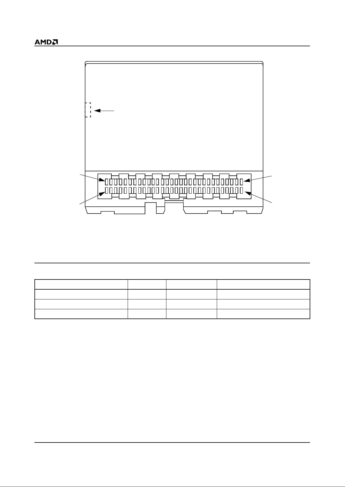
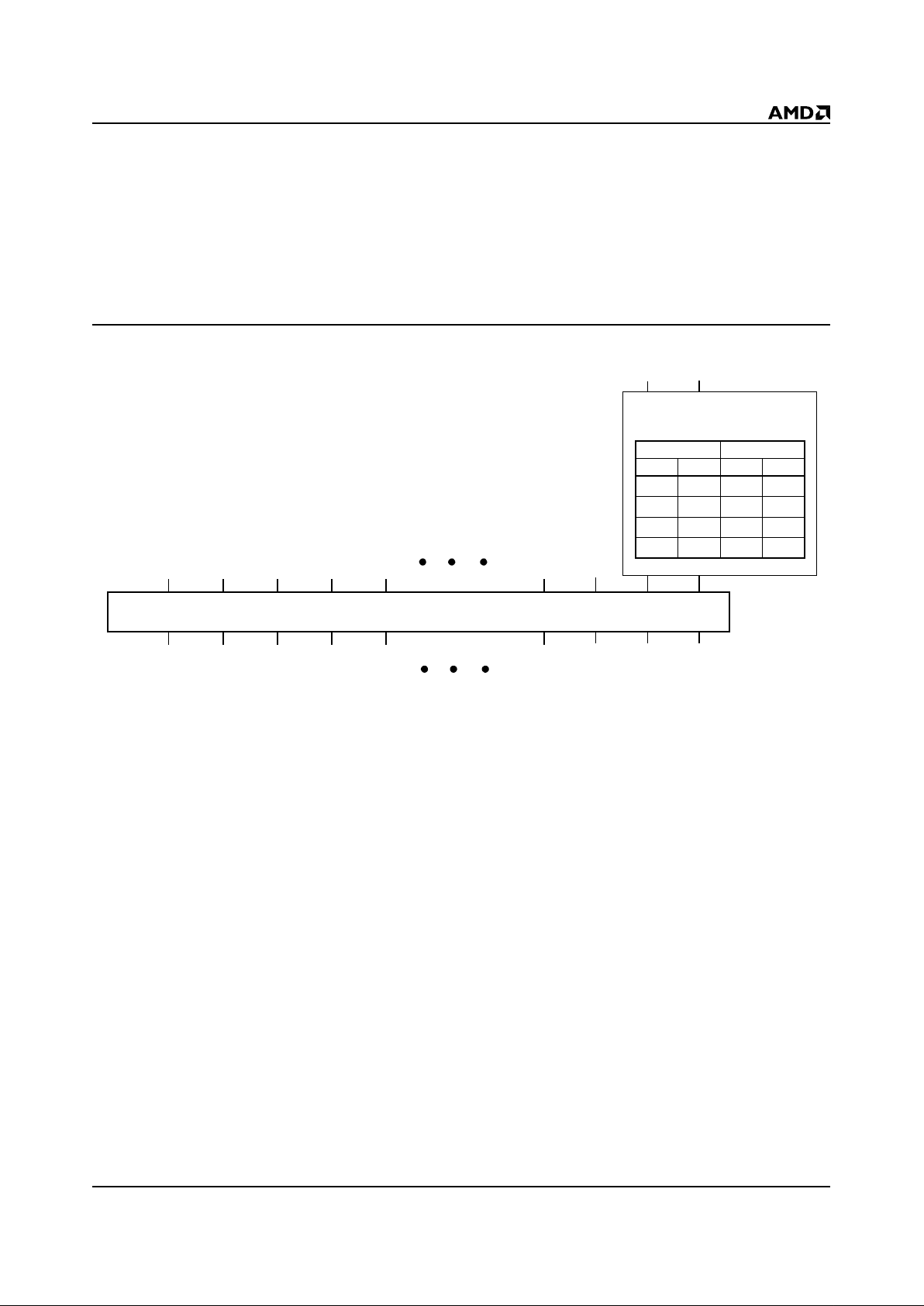
Figure 1. Miniature Card Connector (Card Bottom View)
Note: Refer to the Physical Dimensions section for more information. Also refer to the MCIF specification for detailed mechanical
information, available on the Web at http://www.mcif.org.
Table 2. AMD Flash Miniature Cards and Flash Devices
Family Part Number Density No. of Flash Devices AMD Flash Memory
AmMC002AWP 2 Mbyte 2 Am29F080B
AmMC004AWP 4 Mbyte 2 Am29F017B
AmMC008AWP 8 Mbyte 4 Am29F017B
Write Protect Swit ch (opt i onal)
Pad 60 Pad 31
Pad 30 Pad 1
V
CC
CINS# GND
3V/5V
Key
Alignment
Notch
20975D-1
Page 5
AmMC0XXA 5
PRELIMINARY
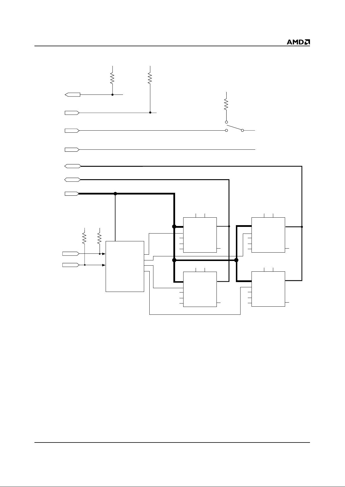
BLOCK DIAGRAM
* Decoder used on 8 Mbyte card only. Not used on 2 and 4 Mbyte cards.
** 2 Mbyte card: Two Am29F080B devices, S0 and S1
4 Mbyte card: Two Am29F017B devices, S0 and S1
8 Mbyte card: Four Am29F017B devices, S0...S3
*** A0–A19 on 2 Mbyte card; A0–A20 on 4 and 8 Mbyte cards.
Note: On the 2 Mbyte card, A20–A24 are not connected. On the 4 Mbyte cards, A21–A24 are not connected. On the 8 Mbyte
cards, A22-A24 are not connected. Connections not shown in this diagram are not connected internally.
OE#
BUSY#
RY/BY#
A0–A24
Decoder*
CEL#
100K
100K
CEH#
WE#
WE# to all Flash devices
Write Protect
Switch
CEL0#
CEH0#
CEL1#
CEH1#
A21
V
CC
10K
V
CCVCC
OE# to all Flash devices
D0–D7
D8–D15
RESET#
RESET# to all Flash devices
A0-A20***
WE#
OE#
D8-D15
V
SSVCC
RESET#
RY/BY#
S1**
A0-A20***
CE#
WE#
OE#
D0-D7
V
SSVCC
RESET#
RY/BY#
S2**
A0-A20***
CE#
WE#
OE#
D8-D15
V
SSVCC
RESET#
RY/BY#
S3**
A0-A20***
CE#
WE#
OE#
D0-D7
V
SSVCC
RESET#
RY/BY#
S0**
V
CC
10K
V
CC
10K
20975D-2
Page 6

6AmMC0XXA
PRELIMINARY
MINIATURE CARD PAD ASSIGNMENTS
A0–A24
Address A0 to A24 are the address bus lines that can
address up to 32 Mwords (64 Mbytes). The address
lines are word addressed. The Miniature Card specification does not require the Miniature Card to decode
the upper address lines. A 2 Mbyte Miniature Card that
does not decode the upper address lines would repeat
its address space every 2 Mbytes. Address 0h would
access the same physical location as 200000h,
400000h, 600000h, e tc. On the 2 Mbyte cards, A20 –
A24 are not connected. On the 4 Mbyte cards, A21–
A24 are not connected. On the 8 Mbyte cards, A22–
A24 are not connected.
D0–D15
Data lines D0 through D15 constitute the data bus . The
data bus is composed of two bytes; the low byte is D0–
D7 and the high byte is D8–D15. These lines are
tristated when OE# is high.
OE#
OE# indicates to the card that the current bus cycle is
a read cycle. The output enable access time (t
OE
) is the
delay from the falling edge of OE# to valid data at the
output pins (assuming the addresses h a ve been stable
for at least t
ACC
– tOE time).
WE#
WE# indicates to the card that the current bus cycle is a
write cycle. The fall ing edge of WE# latches addr ess in f or mation and the rising edge latches data/command information.
VS1#
Voltage Sense 1 signal. T his signal is left open or
not connected.
VS2#
Voltage Sense 2 signal. T his signal is left open or
not connected.
CEL#
CEL# enables the low byte of t he data b us (D0 –D7) on
the card.
CEH#
CEH# enables the high byte of the data bus (D8–D15)
on the card.
RESET#
RESET# controls card initialization. When RESET#
transitions from a low state to a high state, the Miniature Card resets to the Read state.
BUSY#
BUSY# is a signal generated b y t he card to indic ate the
status of operations w ithin the Miniature Card. When
BUSY# is high, the Miniature Card is ready to accept
the next command from the host. When BUSY# is low,
the Miniature Card is busy and unable to accept most
data operations from the host. In Flash Miniature Cards
the BUSY# signal is tied to th e components’ RY/BY#
signal.
CD#
CD# is a grounded interface signal. After a Miniature
Card has been inserted, CD# will be forced low. The
card detect signal is located in the center of the second
row of interface signals, and should be one of the last
interface signals to connect t o the host . Do not c onfuse
CD# with CINS#.
CINS#
CINS# is a grounded signal on the front of th e Miniature
Card that is used for early detection of a card insertion.
CINS# makes contact on the host when the front of the
card is inserted into the socket, before the interface
signals connect.
BS8#
The BS8# (Bus size 8) signal indicates t o the Mini ature
Card that the host has an 8-bit bus. AMD Flash Miniature Cards ignore this signal. An 8-bit host must
connect its D0–D7 data lines to D8–D15 on the Miniature Card to retrieve the upper (odd) byte.
GND
Ground
V
CC
Vcc is used to supply power to the card.
NC
No connect
RFU
Reserved for future use
Page 7
AmMC0XXA 7
PRELIMINARY
ORDERING INFORMATION
Standard Pr od ucts
AMD standard products are available in several packages and operating ranges. The order number (Valid Combination) is formed
by a combination of the following:
Valid Combinations
Valid Combinations list configurations planned to be supported in volume for this device. Consult the local AMD sales
office to confirm availability of specific valid combinations and
to check on newly released combinations.
AM MC 008
SPEED OPTION
See Valid Combinations below
MINIATURE CARD
MEMORY CARD DENSITY
002 = 2 Megabyte Card
004 = 4 Megabyte Card
008 = 8 Megabyte Card
AMD
A
REVISION LEVEL
-100 I
TEMPERATURE RANGE
Blank = Commerc ial (0°C to +70°C)
I=Industrial (–40°C to +85°C)
WP
WRITE PROTECT SWITCH OPTION
WP = Switch installed
Valid Combinations
AmMC002AWP
-100, -100I, -150AmMC004AWP
AmMC008AWP
Page 8
8AmMC0XXA
PRELIMINARY
INTERFACE SIGNAL ASSIGNMENTS
Note: NC = No Connect; RFU = Reserved for Future Use.
FLASH MINIATURE CARD OPERATIONS
Voltage Sensing
AMD Miniature Cards provide two voltage sense
signals for hosts that support multiple voltages. The
multivoltage hos t can sense the voltage level of the
Miniature Card and power up th e card at that voltag e.
See Table 3 for a description of the voltage sense
signals.
In addition to the voltage sense pins, there are also
mechanical voltage keys on the Miniature Card that
ensure the card can only be inserted into host systems
that can supply the proper voltage levels to the card.
Refer to Section 4.1.2 in the Miniature Card specification for more information on mechanical keying.
Table 3. Voltage Sense Signals
Pad Number Signal Name Pad Number Signal Name Pad Number Signal Name
1A1821D1241A4
2 A16 22 D10 42 CEL#
3 A14 23 D9 43 A1
4NC24D044NC
5CEH#25 D2 45 NC
6 A11 26 D4 46 CD#
7 A9 27 RFU 47 A21
8 A8 28 D7 48 BUSY#
9A629NC49WE#
10 A5 30 NC 50 D14
11 A3 31 A19 51 RFU
12 A2 32 A17 52 D11
13 A0 33 A15 53 VS2#
14 NC 34 A13 54 D8
15 A24 35 A12 55 D1
16 A23 36 RESET# 56 D3
17 A22 37 A10 57 D5
18 OE# 38 VS1# 58 D6
19 D15 39 A7 59 RFU
20 D13 40 BS8# 60 A20
Miniature Card
Power-Up Voltage VS1# VS2#
5 Volt-only Open Open
Page 9
AmMC0XXA 9
PRELIMINARY
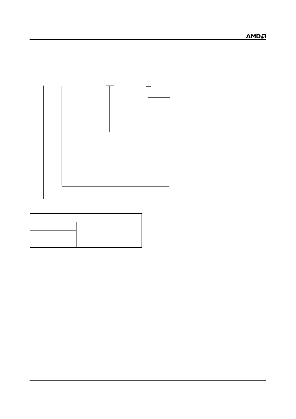
Data Accesses
The Miniature Card has a 16-bit data bus that can
accommodate word or byte acces ses. By individually
asserting CEL# and CEH#, a host can access either
byte. However, byte swapping (moving the high byte
data to the low byte) is not supported.
Figure 2 shows the connections between the host and
Miniature Card. The host system address lines range
from A0-A25, whereas the Miniature C ard address
lines range from A0–A24. On the host, A0 and the
byte/word line are sent to a decoder and ou tput to
CEL# and CEH# on the Miniature Card. These two bits
enable a single device for byte accesses and two
devices for word accesses, as shown by the decoder
truth table in Figure 2. Again, the Miniature Card
address lines do not receive input from host addre ss bit
A0. In this document, all address references are
card
addresses
, unless otherwise noted. Table 4 shows the
read/write modes for Miniature Cards.
* Not connected on 2 Mbyte card
** Not connected on 2 and 4 Mbyte card
*** Not connected
Figure 2. Host/Card Address Connections
Host
Byte/Word
A0
A1A25
Card CEH#CEL#A0
A24
A23***A24***
A23
A22***
A22
A21**
60-Pad Connector
A2
A1
Decoder
Decoder Truth Table
Input Output
A0 B/W CEL CEH#
0000
0101
1000
1110
20975D-3
Host Bus
Card Bus
A21
A20*
Page 10
10 AmMC0XXA
PRELIMINARY
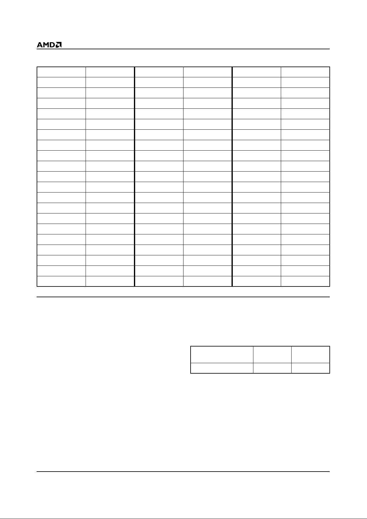
Table 4. Miniature Card Read/Write Modes
Notes:
1. Unlisted access combinations are invalid and may return unexpected results.
2. X indicates a Don’t Care value.
Erase Operations
The AMD Flash Miniature Card is organized as an array
of individual devices. On the 2 Mbyte Miniature Card,
each Am29F080B device contains sixteen 64 Kbyte sectors, for a total of 1 Mbyte of memory space per device.
On 4 and 8 Mbyte Miniature Cards, each Am29F017B
device contains thirty-two 64 Kbyte sectors, for a total of
2 Mbytes of memory space per device.
Flash technology allows any logical “1” data bit to be programmed to a logical “0”. The only way to reset bits to a
logical “1” is to erase that entire memor y sector or
memory device. Once a memory sector or memory
device is erased, any address location may be programmed. Two or more devices may be erased concurrently when additional I
CC
current is supplied to the card.
However, erasing more than two de vices concurrently is
not typical in battery-powered applications, but may take
place during procedures such as card testing.
Since erase commands operate on entire sectors or
devices, the host should track the affected memory
addresses; for example, by determining the sector size
and device size and calculating the corresponding
addresses.
Erase operations can be performed in several ways:
■ Erase a single sector or mult iple sectors in a de v ice
■ Erase a sector pair
■ Erase multiple device pairs *
■ Erase the entire card *
* This operation is only feasible in solutions capable of
supplying more tha n the specified miniature car d
supply current requirement (150 mA) per system. Each
AMD Flash memory device pair will require a
maximum of 120 mA supply current.
The common memory space data contents are altered
in a similar manner as writing to individual Flash memory
devices. An on-card address decoder activates the
appropriate Flash device in the memory array. Each
device internally latches addre ss and data during write
cycles. Refer to Table 4.
Word-Wide Operations
The AMD Miniature Card provide the flexibility to operate
on data in a byte-wide or word-wide format. In word-wide
operations, the low bytes are controlled with CEL#. The
high bytes are controlled with CEH# . Refer to the block
diagram for more information.
Byte-Wide Operations
Byte-wide data is available for read and write operations (CEL# = 0, CEH# = 1). Even and odd bytes are
stored in separate memory devices (for example, S0
and S1) and are accessed by controlling CEL# and
CEH#. The even b yt e is t he lo w order byte and the odd
byte is the high order byte of a 16-bit word.
Each memory sector or device pair must be addressed
separately for erase operations. Refer to the block
diagram for more information.
Card Detection
Each CD# (output) pin should be detected by the host
system to determine if the memory card is adequately
seated in the socket. CD# and CINS# are internally tied
to ground. If both bits are not de tected, the system
should indicate that the card must be re-inserted.
Function CEH# CEL# WE# OE# D8–D15 D0–D7
Read Mode
Standby H H X X High-Z High-Z
Word Access L L H L High Byte Data Low Byte Data
Low Byte Access H L H L High-Z Low Byte Data
High Byte Access L H H L High Byte Data High-Z
Write Mode
Standby H H X X High-Z High-Z
Word Access L L L H High Byte Data Low Byte Data
Low Byte Access H L L H High-Z Low Byte Data
High Byte Access L H L H High Byte Data High-Z
Page 11
AmMC0XXA 11
PRELIMINARY
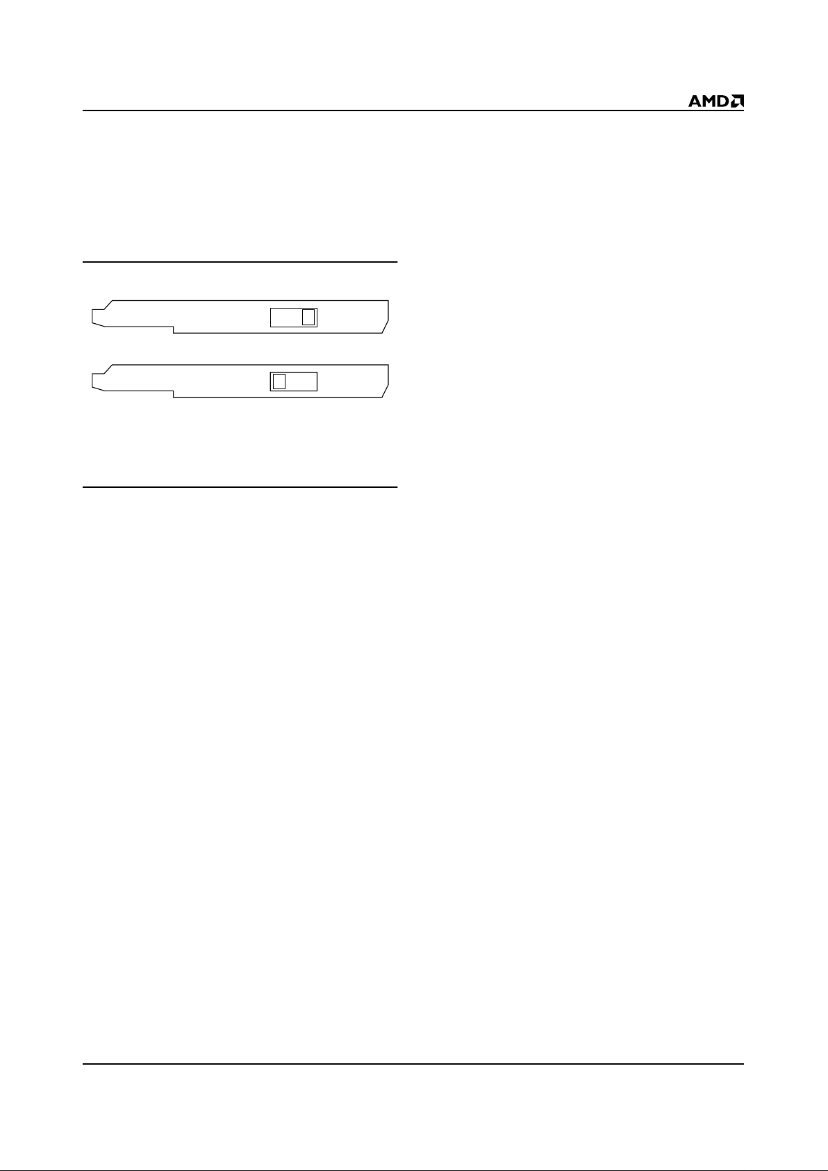
Data Protection
An optional mechanical write protect switch provides
user-initiated write protection. When this switch is activated, WE
# is internally forced high. The Flash memory
command register is disabled from accepting any write
commands. This prevents the card from responding to
any commands (for e xample, an Aut oselect command).
See Figure 3.
Figure 3. Write Protect Switch
(Card Right Side View)
In addition to card-level data protection, AMD Flash
Miniature Cards offer several device-level data protection features.
Device-Level Data Protection
AMD Flash memory devices offer protection against
accidental erasure or programming caused by spurious
system level signals that may e xist during power tr ansitions. During power up, each device automatically
resets the internal state machine to the read mode. The
control register architecture allows alteration of the
memory contents only occurs after successful completion of specific multi-bus cycle command sequences.
AMD Flash memory devices also incorporate the following features to prevent inadvertent write cycles
resulting from V
CC
power-up and power-down
transitions or system noise.
Low V
CC
Write Inhibit
To avoid initiation of a write cycle during V
CC
powerup and power-down, the AMD memory devices in
the Miniature Card lock out write cycles for V
CC
<
V
LKO
(see “DC Characteristics ” o n page 25 for volt-
ages). When V
CC
< V
LKO
, the command register is
disabled, all internal program/erase circuits are disabled, and the device resets to the read mode.
These memory devices ignore all w r i tes u ntil V
CC
>
V
LKO
. The user must ensure that the control pins
are in the correct logical state wh en V
CC
> V
LKO
to
prevent unintentional writes.
Write Pulse “Glitch” Protection
Noise pulses of less than 5 ns (typical) on OE#, CE#,
or WE# will neither initiate a write cycle nor change the
command registers.
Logical Inhibit
Writing is inhibited by holding any one of OE# = V
IL
,
CE# = V
IH
, or WE# = VIH. To initiate a write cycle CE#
and WE# must be a logical zero while OE# is a logical
one.
Power-Up Write Inhibit
Pow er-up of the devic e with CE# = WE# = V
IL
and OE#
= V
IH
will not accept commands on the rising edge of
WE#. The internal state machine is automatically reset
to the read mode on power-up.
Read Mode
Two Card Enable (CE#) pins are available on the
memory card. Both CE# pins must be active low for
word-wide read accesses. Only one CE# is required for
byte-wide accesses. The CE# pins select and determine when to apply power to the high-byte and lowbyte memory devices. The Output Enable (OE#) controls gating accessed data from the memor y device
outputs.
The Miniature card au tomatically powers up in the
read/reset state. In this case, a command sequence is
not required to r ead data. Standard mic roprocessor
read cycles will retrieve array data. This default value
ensures that no spurio us alteration of the memory
content occurs during the power transition. Ref er to the
AC Read Characteristics and Waveforms for the specific timing parameters.
Output Disable
Data outputs from the card are disabled when OE# is
at a logic-high lev el. Under this condition, outputs are in
the high-impedance state.
Standby Operations
Byte-wide read accesses only require half of the
read/write output buffer (x16) to be active. In addition,
only one memory device is active within either the high
order or low order bank. Activation of the appropriate
half of the output buff er is controll ed by the combination
of both CE# pins. The CE# pins also control power to
the high and low-order banks of memory. Outputs of
the memory bank not selected are plac ed in the high
impedance state. The individual memory device is activated by the address decoders. The other memory
devices operate in standby. An active memory device
continues to draw power until completion of a write or
erase operation if the card is de-selected in t he process
of one of these operations.
Write Enabled
Write Disabled
20975D-4
Page 12

12 AmMC0XXA
PRELIMINARY
Autoselect Operation
A host system or e xternal card re ader/writer c an determine the on-card manufacturer and device I.D. codes.
Codes are available after writing the 90h command to
the command register of a memory device, as sho wn in
Tables 5 through
10. When the autoselect command is
issued to card address 00000h, the Miniature Card
returns the manufacturer I.D. If the autoselect
command is issued to card address 00001h, the Miniature Card provides the device I.D.
To terminate the Auto Select operation, the
Read/Reset command sequence must be written to the
same device. The Autoselect command operates only
if the card is not write protected.
Sector Group Protection
Sector group protection can be used to permanently
disable program and erase oper ation s in any combination of sector groups on t he Flash memory components
used in AMD Miniature Cards. Each sector group consists of four adjacent sectors within each device. The
pattern begins at SA0: SA0–3, SA4–7, SA8–11, and so
on. This protection must be performed prior to manufacturing the Miniature Cards. None of the sector
groups are protected on the standard Miniature Card
product offerings.
The host system must compensate for these protec ted
sector groups by determining their locations, then
ignoring those locations for reading and writing data. To
determine whether a sector group is protected, the
system would write the first three cycles of the Autoselect command, then on the fourth cycle, read at the
address (SA)02h, where SA is the sector address (see
Tables 11 and 12) within an individual device. A protected sector group produces “01h”, and an unprotected sector group produces “00h”.
Write Operations
Write and erase operations are valid only when VCC is
above 4.5 V. Thi s activates the state machine of a n
addressed memory device. The command register is a
latch which saves address, commands, and data information used by the state machine and memory array.
When Write Ena ble (WE#) and appropriate CE#
signals are at a logi c-level low, and Output Enable
(OE#) is at a logic-high, the comman d register is
enabled for write operations. The falling edge of WE#
latches address information and the rising edge latc hes
data/command information.
Write or erase operations are performed by writing
appropriate data patterns to the com mand register of
accessed Flash memory devices.
The byte-wide commands are defined in Tables 6, 7,
9,
and 10; word-wide commands are defined in Tables 5
and 8. Note that the Erase Suspend (B0h) and Erase
Resume (30h) commands are valid only while the
Sector Erase operation is in progress.
Page 13

AmMC0XXA 13
PRELIMINARY
Table 5. Word Command Definitions for 2 Mbyte Cards
Legend:
X = Don’t care
RA = Address of the memory location to be read.
RW = Data read from location RA during read operation.
PA = Address of the memory location to be programmed.
Addresses are latched on the falling edge of the WE# pulse.
PW = Data to be programmed at location P A. Data is latched
on the rising edge of WE#.
SA = Address of the sector to be erased. Refer to T able 11 f or
sector addresses.
Notes:
1. Write protect must not be enabled for proper operation of
all commands. No command required for reading array
data, and can thus be done with write protect enabled.
2. During word addressing, CEL# = 0, CEH# = 0, and
address is applied to Memory Device Pair 0 (S0 and S1).
For host-to-card address bit connections, see Figure 2.
3. All values are in hexadecimal.
4. The last bus cycle in an autoselect command sequence is
a read operation.
5. Word = high byte + low byte.
6. Address bits A19–A11 = X = Don’t Care for all commands
except for Read Address (RA), Program Address (PA),
and Sector Address (SA).
7. The Erase Suspend command is valid only during a
sector erase operation. Refer to “Sector Erase Suspend”.
8. The Erase Resume command is valid only during the
Erase Suspend mode.
9. See Table 4 for read/write modes.
Embedded Command Sequence
(Note 1)
Bus Cycles (Notes 2–9)
First Second Third Fourth Fifth Sixth
Addr Data Addr Data Addr Data Addr Data Addr Data Addr Data
Read 1 RA RW
Reset 1 XXX F0F0
Autoselect Manufacturer ID (Note 4) 4 555 AAAA 2AA 5555 555 9090 X00 0101
Autoselect Device ID (Note 4) 4 555 AAAA 2AA 5555 555 9090 X01 D5D5
Word Write 4 555 AAAA 2AA 5555 555 A0A0 PA PW
Device Erase 6 555 AAAA 2AA 5555 555 8080 555 AAAA 2AA 5555 555 1010
Sector Erase 6 555 AAAA 2AA 5555 555 8080 555 AAAA 2AA 5555 SA 3030
Sector Erase Suspend (Note 7) 1 XXX B0B0
Sector Erase Resume (Note 8) 1 XXX 3030
Cycles
Page 14

14 AmMC0XXA
PRELIMINARY
Table 6. Even Byte Command Definitions for 2 Mbyte Cards
Note for Table 6: During even (low) byte accesses, CEL# = 0, CEH# = 1, and address is applied to Memory Device 0 (S0) only.
Table 7. Odd Byte Command Definitions for 2 Mbyte Cards
Note for Table 7:During odd (high) byte accesses, CEL#= 1, CEH# = 0, and address is applied to Memory Device 1 (S1) only.
Legend for Tables 6 and 7:
X = Don’t care
RA = Address of the memory location to be read.
RW = Data read from location RA during read operation.
PA = Address of the memory location to be programmed.
Addresses are latched on t he falling edge of the WE# pulse.
PW = Data to be programmed at location PA. Data is latched on
the rising edge of WE#.
SA = Address of the sector to be erased. Refer to Table 11 for
sector addresses.
Notes for Tables 6 and 7:
1. Write protect must not be enabled for proper operation of all
commands. No command required for reading array data,
and can thus be done with write protect enabled.
2. For host-to-card address bit connections, see Figure 2.
3. All values are in hexadecimal.
4. The last cycle of an autoselect command sequence is a read
operation.
5. Address bits A19–A11 = X = Don’t Care for all commands
except for Read Address (RA), Program Address (PA), and
Sector Address (SA).
6. The Erase Suspend command is valid only during a sector
erase operation. Refer to “Sector Erase Suspend”.
7. The Erase Resume command is valid only during the Erase
Suspend mode.
8. See Table 4 for read/write modes.
Embedded Command Sequence
(Note 1)
Bus Cycles (Notes 2–9)
First Second Third Fourth Fifth Sixth
Addr Data Addr Data Addr Data Addr Data Addr Data Addr Data
Read 1 RA RD
Reset 1 XXX XXF0
Autoselect Manufacturer ID (Note 4) 4 555 XXAA 2AA XX55 555 XX90 X00 XX01
Autoselect Device ID (Note 4) 4 555 XXAA 2AA XX55 555 XX90 X01 XXD5
Byte Write 4 555 XXAA 2AA XX55 555 XXA0 PA PD
Device Erase 6 555 XXAA 2AA XX55 555 XX80 555 XXAA 2AA XX55 555 XX10
Sector Erase 6 555 XXAA 2AA XX55 555 XX80 555 XXAA 2AA XX55 SA XX30
Sector Erase Suspend (Note 6) 1 XXX XXB0
Sector Erase Resume (Note 7) 1 XXX XX30
Embedded Command Sequence
(Note 1)
Bus Cycles (Notes 2–9)
First Second Third Fourth Fifth Sixth
Addr Data Addr Data Addr Data Addr Data Addr Data Addr Data
Read 1 RA RD
Reset 1 XXX F0XX 2AA 55XX 555 F0XX RA RD
Autoselect Manufacturer ID (Note 4) 4 555 AAXX 2AA 55XX 555 90XX X00 01XX
Autoselect Device ID (Note 4) 4 555 AAXX 2AA 55XX 555 90XX X01 D5XX
Byte Write 4 555 AAXX 2AA 55XX 555 A0XX PA PDXX
Device Erase 6 5 55 AAXX 2AA 55XX 555 80XX 555 AAXX 2AA 55X X 555 10XX
Sector Erase 6 555 AAXX 2AA 55XX 555 80XX 555 AAXX 2AA 55XX SA 30XX
Sector Erase Suspend (Note 6) 1 XXX B0XX
Sector Erase Resume (Note 7) 1 XXX 30XX
Cycles
Cycles
Page 15

AmMC0XXA 15
PRELIMINARY
Table 8. Word Command Definitions for 4 and 8 Mbyte Cards
Legend:
X = Don’t care
RA = Address of the memory location to be read.
RW = Data read from location RA during read operation.
PA = Address of the memory location to be programmed.
Addresses are latched on the falling edge of the WE# pulse.
PW = Data to be programmed at location P A. Data is latched
on the rising edge of WE#.
SA = Address of the sector to be erased. Refer to T able 12 f or
sector addresses.
Notes:
1. Write protect must not be enabled for proper operation of
all commands. No command required for reading array
data, and can thus be done with write protect enabled.
2. During word addressing, CEL# = 0, CEH# = 0, and
address is applied to Memory Device Pair 0 (S0 and S1).
On 8 Mbyte cards, address for Memory Device Pair 1 =
(Addr) + 400000h, and address is applied to S2 and S3.
For host-to-card address bit connections, see Figure 2.
3. All values are in hexadecimal.
4. The last bus cycle in an autoselect command sequence is
a read operation.
5. Word = high byte + low byte.
6. Address bits A19–A11 = X = Don’t Care for all commands
except for Read Address (RA), Program Address (PA),
and Sector Address (SA).
7. The Erase Suspend command is valid only during a
sector erase operation. Refer to “Sector Erase Suspend”.
8. The Erase Resume command is valid only during the
Erase Suspend mode.
9. See Table 4 for read/write modes.
Embedded Command Sequence
(Note 1)
Bus Cycles (Notes 2–9)
First Second Third Fourth Fifth Sixth
Addr Data Addr Data Addr Data Addr Data Addr Data Addr Data
Read 1 RA RW
Reset 1 XXXX F0F0
Autoselect Manufacturer ID (Note 4) 4 XXXX AAAA XXXX 5555 XXXX 9090 XX00 0101
Autoselect Device ID (Note 4) 4 XXXX AAAA XXXX 5555 XXXX 9090 XX01 3D3D
Word Write 4 XXXX AAAA XXXX 5555 XXXX A0A0 PA PW
Device Erase 6 XXXX AAAA XXXX 5555 XXXX 8080 XXXX AAAA 2AAA 5555 XXXX 1010
Sector Erase 6 XXXX AAAA XXXX 5555 X XXX 8080 XXXX AAAA 2AAA 5555 SA 3030
Sector Erase Suspend (Note 7)
1
XXXX B0B0
Sector Erase Resume (Note 8)
1
XXXX 3030
Cycles
Page 16

16 AmMC0XXA
PRELIMINARY
Table 9. Even Byte Command Definitions for 4 and 8 Mbyte Cards
Note for T able 9: During high byte addressing, CEL# = 1, CEH# = 0, and address applied to Memory Device 1 (S1) = (Addr) + 200000h.
On 8 Mbyte cards, address for S3 = (Addr) + 400000h + 200000h.
Table 10. Odd Byte Command Definitions for 4 and 8 Mbyte Cards
Note for T able 7: During low byte addressing, CEL# = 0, CEH# = 1, and address applied to Memory Device 0 (S0) = (Addr). On 8 Mbyte
cards, address for S2 = (Addr) + 400000h.
Legend for Tables 6 and 7:
X = Don’t care
RA = Address of the memory location to be read.
RW = Data read from location RA during read operation.
PA = Address of the memory location to be programmed.
Addresses are latched on t he falling edge of the WE# pulse.
PW = Data to be programmed at location PA. Data is latched on
the rising edge of WE#.
SA = Address of the sector to be erased. Refer to Table 11 for
sector addresses.
Notes for Tables 6 and 7:
1. Write protect must not be enabled for proper operation of all
commands. No command required for reading array data,
and can thus be done with write protect enabled.
2. For host-to-card address bit connections, see Figure 2.
3. All values are in hexadecimal.
4. The last cycle of an autoselect command sequence is a read
operation.
5. Address bits A19–A11 = X = Don’t Care for all commands
except for Read Address (RA), Program Address (PA), and
Sector Address (SA).
6. The Erase Suspend command is valid only during a sector
erase operation. Refer to “Sector Erase Suspend”.
7. The Erase Resume command is valid only during the Erase
Suspend mode.
8. See Table 4 for read/write modes.
Embedded Command Sequence
(Note 1)
Bus Cycles (Notes 2–9)
First Second Third Fourth Fifth Sixth
Addr Data Addr Data Addr Data Addr Data Addr Data Addr Data
Read 1 RA RD
Reset 1 XXXX XXF0
Autoselect Manufacturer ID (Note 4) 4 XXXX XXAA XXXX XX55 XXXX XX90 XX00 XX01
Autoselect Device ID (Note 4) 4 XXXX XXAA XXXX XX55 XXXX XX90 XX01 XX3D
Byte Write 4 XXXX XXAA XXXX XX55 XXXX XXA0 PA PD
Device Erase 6 XXXX XXAA XXXX XX55 XXXX XX80 XXXX XXAA XXXX XX55 XXXX XX10
Sector Erase 6 XXXX XXAA XXXX XX55 XXXX XX80 XXXX XXAA XXXX XX55 SA XX30
Sector Erase Suspend (Note 6) 1 XXXX XXB0
Sector Erase Resume (Note 7) 1 XXXX XX30
Embedded Command Sequence
(Note 1)
Bus Cycles (Notes 2–9)
First Second Third Fourth Fifth Sixth
Addr Data Addr Data Addr Data Addr Data Addr Data Addr Data
Read 1 RA RD
Reset 1 XXXX F0XX
Autoselect Manufacturer ID (Note 4) 4 XXXX AAXX XXXX 55XX XXXX 90XX XX00 01XX
Autoselect Device ID (Note 4) 4 XXXX AAXX XXXX 55XX XXXX 90XX XX01 3DXX
Byte Write 4 XXXX AAXX XXXX 55XX XXXX A0XX PA PD
Device Erase 6 XXXX AAXX XXXX 55XX XXXX 80XX XXXX AAXX XXXX 55XX XXXX 10XX
Sector Erase 6 XXXX AAXX XXXX 55XX XXXX 80XX XXXX AAXX XXXX 55XX SA 30XX
Sector Erase Suspend (Note 6) 1 XXXX B0XX
Sector Erase Resume (Note 7) 1 XXXX 30XX
CyclesCycles
Page 17

AmMC0XXA 17
PRELIMINARY
Table 11. Memory Sector Addresses for 2 Mbyte Card
Notes:
1. For word addressing, devices 0 and 1 (S0 and S1) together form Memory Device Pair 0. Refer to the block diagram for device
connections.
2. Card address bits range from A0 to A19. Host address bits range from A0 to A20. Host address bit A0 is used for controlling
the CEL# and CEH# inputs to the card. Refer to Figure 2 for host-to-card address bit connections.
Sector
Card Address Bits Device 0 and/or 1 (Note 1)
A19 A18 A17 A16 Card Address Range
0 0000 00000h–0FFFFh
1 0001 10000h–1FFFFh
2 0010 20000h–2FFFFh
3 0011 30000h–3FFFFh
4 0100 40000h–4FFFFh
5 0101 50000h–5FFFFh
6 0110 60000h–6FFFFh
7 0111 70000h–7FFFFh
8 1000 80000h–8FFFFh
9 1001 90000h–9FFFFh
10 1010 A0000h–AFFFFh
11 1011 B0000h–BFFFFh
12 1100 C0000h–CFFFFh
13 1101 D0000h–DFFFFh
14 1110 E0000h–EFFFFh
15 1111 F0000h–FFFFFh
Page 18

18 AmMC0XXA
PRELIMINARY
Table 12. Memory Sector Addresses for 4 and 8 Mbyte Cards
Notes:
1. For word addressing, devices 0 and 1 (S0 and S1) together form Memory Device Pair 0; devices 2 and 3 (S2 and S3) form
Memory Device Pair 1. Refer to the block diagram for device connections.
2. The 4 Mbyte card address bits range from A0 to A20. Host address bits range from A0 to A21. Host address bit A0 is used
for controlling the CEL# and CEH# inputs to the card. Refer to Figure 2 for host-to-card address bit connections.
3. The 8 Mbyte card address bits range from A0 to A21. A21 is used to select devices 2 and 3 (S2 and S3). Host address bits
range from A0 to A22. Host address bit A0 is used for controlling the CEL# and CEH# inputs to the card. Refer to Figure 2
for host-to-card address bit connections.
Sector
Card Address Bits Device 0 and/or 1 Device 2 and/or 3
A20 A19 A18 A17 A16
Card Address Range
(Note 2)
Card Address Range
(Notes 2, 3)
0 00000 00000h–0FFFFh 200000h–20FFFFh
1 00001 10000h–1FFFFh 210000h–21FFFFh
2 00010 20000h–2FFFFh 220000h–22FFFFh
3 00011 30000h–3FFFFh 230000h–23FFFFh
4 00100 40000h–4FFFFh 240000h–24FFFFh
5 00101 50000h–5FFFFh 250000h–25FFFFh
6 00110 60000h–6FFFFh 260000h–26FFFFh
7 00111 70000h–7FFFFh 270000h–27FFFFh
8 01000 80000h–8FFFFh 280000h–28FFFFh
9 01001 90000h–9FFFFh 290000h–29FFFFh
10 01010 A0000h–AFFFFh 2A0000h–2AFFFFh
11 01011 B0000h–BFFFFh 2B0000h–2BFFFFh
12 01100 C0000h–CFFFFh 2C0000h–2CFFFFh
13 01101 D0000h–DFFFFh 2D0000h–2DFFFFh
14 01110 E0000h–EFFFFh 2E0000h–2EFFFFh
15 01111 F0000h–FFFFFh 2F0000h–2FFFFFh
16 10000 100000h–10FFFFh 300000h–30FFFFh
17 10001 110000h–11FFFFh 310000h–31FFFFh
18 10010 120000h–12FFFFh 320000h–32FFFFh
19 10011 130000h–13FFFFh 330000h–33FFFFh
20 10100 140000h–14FFFFh 340000h–34FFFFh
21 10101 150000h–15FFFFh 350000h–35FFFFh
22 10110 160000h–16FFFFh 360000h–36FFFFh
23 10111 170000h–17FFFFh 370000h–37FFFFh
24 11000 180000h–18FFFFh 380000h–38FFFFh
25 11001 190000h–19FFFFh 390000h–39FFFFh
26 11010 1A0000h–1AFFFFh 3A0000h–3AFFFFh
27 11011 1B0000h–1BFFFFh 3B0000h–3BFFFFh
28 11100 1C0000h–1CFFFFh 3C0000h–3CFFFFh
29 11101 1D0000h–1DFFFFh 3D0000h–3DFFFFh
30 11110 1E0000h–1EFFFFh 3E0000h–3EFFFFh
31 11111 1F0000h–1FFFFFh 3F0000h–3FFFFFh
Page 19

AmMC0XXA 19
PRELIMINARY
PROGRAM AND ERASE OPERATIONS
AMD Flash Memory devices include Embedded
Algorithms (Embedded Erase and Embedded Program) that allow the host to simply issue a command,
after which it is free to perform other tasks. The host
then only needs to monitor appropriate status bits to
determine when the operation is complete.
Embedded Erase Algorithm
When erasing a sector or device , the Embe dded Erase
algorithm does not require the host to first entirely preprogram the device. Upon executing the Embedded
Erase command sequence, the addressed memory
sector or memory device automatically writes and verifies the entire memory device or memory sector for an
all “0” data pattern. The system is not required to
provide any controls or timi ng during the se operations.
When the memory sector or memory device is automatically verified to contain an a ll “0” pattern, a
self-timed chip erase-and-verify begins . The er ase and
verify operations are complete when the data on D7
(D15 on the odd byte) of the memory sector or memory
device is “1” (see Wr ite Operation Status s ection), at
which time the device returns to the read mode. The
system is not required to provide any control or timing
during these operations. If a Reset command is issued
while the erase operation is in progress, the erase
operation will stop, and the data in that device will be
undefined. In that case, restart the erase on that sector
and allow it to complete.
When using the Embedded Erase algorithm, the erase
automatically terminates when adequate erase margin
has been achieved for the memory array (no erase
verify command is required). The margin voltages are
internally generated in the same manner as when the
standard erase verify command is used.
The Embedded Erase command sequence is a
command only operation that s tages the memory
sector or memory device for automatic electrical
erasure of all bytes in the array. The automatic erase
begins on the rising edge of the WE# and terminates
when the data on D7 of the memory sector or memory
device is “1” (see Write Operation Status section) at
which time the device returns to the Read mode.
Please note that for the memory device or memory
sector erase operation, Dat a Polling may be per formed
at any address in that device or sector.
Figure 4 and Table 13 illustrate the Embedded Erase
Algorithm, a typical command string and bus operations.
As described earlier, once the memor y sector in a
device or memory device completes the Embedded
Erase operation, it returns to the Read mode and
addresses are no longer latched. Theref ore , the de vice
requires that a valid address input to the device is
supplied by the system at this p articular instant of time.
Otherwise, the syst em will never read a “1” on D7. A
system designer has the following choices to
implement the Embedded Erase algorithm:
1. The host may keep the sector address (within any
of the sectors being erased) valid during the entire
Embedded Erase operation.
2. Once the system executes the Embedded Erase
command sequence, the host may remove the address from the dev i ce and perform other tasks. The
host is required to keep track of the v alid sector address by loading it into a temporary register. When
the host comes back to Data P oll t he de vice , it must
reassert the same address.
3. The host may monitor BUSY# (RY/BY#) to determine the status of the Embedded Algorithm in
progress. A “0” indicates that the device is busy; a
“1” indicates that the algorithm is complete.
Sector Erase
Sector erase is a six bus cycle operation. There are
two “unlock” write cycles. These are followed by
writing the “set-up” command. Two more “unlock”
write cycles are then followed by the sector erase
command. The sector address (any address location
within the desired sector) is lat ched on the f alling e dge
of
WE# (or CE#), whichever occurs later, while the
command (data) is latched on the rising edge of the
WE# (or CE#) pulse, whichever occurs first. A
time-out of 100 µs from the rising edge of the last
sector erase command will initiate the sector erase
command(s)
Multiple sectors may be queued for concurrent erase
by writing the six bus cycle operations as described
above. This sequence is followed with writes of the
sector erase command 30h to addresses in other
sectors desired to be concurrently erased. A time-out
of 100 µs from the rising edge of the WE# (or CE#)
pulse for the last sector erase command will initiate the
sector erase. If another sector erase command is
written within the 100 µs time-out window the timer is
reset. Any command other than sector erase within the
time-out window will reset the device to the read mode ,
ignoring the previous command string (refer to Write
Operation Status section for Sector Erase Timer operation). Loading the sector erase buffer may be done in
any sequence and with any sector number.
Sector erase does not require the user to program the
device prior to erase. The device automatically programs all memory locations in the sector(s) to be
erased prior to electrical erase. When erasing a sector
or sectors, the remaining unselected sectors are not
affected. The system is not required to provide any
controls or timings during these operations. A Reset
command issued after the device has begun e xecution
stops the erase operation, b ut the dat a in the sector will
Page 20

20 AmMC0XXA
PRELIMINARY
be undefined. In that case, restart the erase on that
sector and allow it to complete.
The automatic sector erase begins after the 100 µs
time out from the rising edge of the WE# (or CE#)
pulse for the last sector erase command pulse and
terminates when the data on D7 is “1” (see Write
Operation Status section) at which time the device
returns to read mode. Data Polling must be performed at an address within any of the sectors being
erased.
Figure 4 illustrates the Embedded Erase Algorithm
using typical command strings and bus operations.
Table 13. Embedded Erase Algorithm
Figure 4. Embedded Erase Algorithm
Note: The latest release of the software drivers for AMD
Miniature Cards and devices may be downloaded from the
AMD web site at http://www.amd.com.
Embedded Program Algorithm
The Embedded Program setup is a f our bus c ycle operation that stages the addr essed memory sector or
memory device for automatic programming.
Once the Embedded Program setup operation is performed, the next WE
# (or CE#) pulse causes a transi-
tion to an active programming operation. Addresses
are internally latched on the falling edge of the WE
# (or
CE#) pulse. Data is internally latched on the rising
edge of the WE
# pulse. The rising edge of WE# also
begins the programming operation. The system is not
required to provide further control or timing. The device
will automatically provide an adequate internally generated write pulse and verify margin. The automatic programming operation is completed when the dat a on D7
of the addressed memory sector or memory device is
equivalent to data written to this bit (see Write Operation Status section) at which time the device returns to
the Read mode (no write verify command is required).
Addresses are latched on the falling edge of WE
#
during the Embedd ed Program command execution
and hence the system is not required to keep the
addresses stable during the entire Programming operation. However, once the device completes the
Embedded Program operation, it returns to the R ead
mode and addresses are no longer latched. Therefore,
the device requires that a valid address input to the
device is supplied by the system at this particular
instant of time. Otherwise, the system will ne ver read a
valid data on D7. A s ystem designer has two choices to
implement the Embedded Programming algorithm:
1. The system (CPU) keeps the address valid during
the entire Embedded Programming operation, or
2. Once the system executes the Embedded Progr amming command sequence, the CPU takes away the
address from the device and becomes free to do
other tasks. In this case, th e CPU is required to
keep track of the valid address by loading it into a
temporary register. When the CPU comes back for
performing Data Polling, it should reassert
the same address.
3. The host may monitor BUSY# (RY/BY#) to determine the status of the Embedded Algorithm in
progress. A “0” indicates that the device is busy; a
“1” indicates that the algorithm is complete.
Howev er , since the Embedded Prog ramming operation
takes only 8 µs typically, it may be easier for the CPU
to keep the address stab le during the entire Embedded
Programming operation instead of reasserting the valid
address during Data Polling. Anywa y, this has been left
to the system designer’s choice to go for either operation. Any commands writte n to the device during this
period will be ignored. Figure 5 and Table 14 illustrate
the Embedded Program Algorithm, a typical command
string, and bus operation.
Bus
Operation Command Comments
Standby Wait for V
CC
ramp
Write
Embedded Erase
command sequence
6 bus cycle operation
Read
Data Poll or check
BUSY# (RY/BY#) to
verify erasure
Write Embedded Erase
Command Sequence
(See Tables 5–10)
Data Poll from Device
or wait for BUSY#
(RY/BY#)
Start
Erasure Complete
20975D-5
Page 21

AmMC0XXA 21
PRELIMINARY
Table 14. Embedded Program Algorithm
Figure 5. Embedded Program Algorithm
Reset Command
The device automatically powers up in the read/reset
state. A command sequence is not required to read
data in this case. Standard microprocessor cycles retrieve array data. This default state ensures that no
spurious alteration of the memory content occurs during the power transition. Refer to the AC Characteristics section for the specific timing parameters.
The reset operation is initiated by writing the rea d/reset
command sequence into the command register. Microprocessor read cycles retrieve array data from the
memory. The device remains enabled for reads until
the command register contents are altered.
Sector Erase Suspend
Sector Erase Suspend command allows the user to interrupt the chip and then do data reads (not program)
from a non-busy sector while it is in the middle of a Sector Erase operation (which may take up to several seconds). This command is applicable ONLY during the
Sector Erase operation and will be ignored if written
during the chip Erase or Programming operation. The
Erase Suspend command (B0h) will be allowed only
during the Sector Erase Operation that will include the
sector erase time-out period after the Sector Erase
commands (30h). Writing this command during the
time-out will result in immediate termination of the
time-out period. Any subsequent writes of the Sector
Erase command will be ignored as such, but instead
will be taken as the Erase Resume command. Note
that any other commands during the time out will reset
the device to read mode. The addresses are
don’t-cares in writing the Erase Suspend or Erase Resume commands.
When the Sector Erase Suspend command is written
during a Sector Erase operation, the chip will take between 0.1 µs to 10 µs to suspend the erase operation
and go into erase suspended read mode (pseudo-read
mode), during which the user can read from a sector
that is NOT being erased. A read from a sector being
erased may result in invalid data. The user must monitor D6 to determine if the chip has entered the pseudo-read mode, at which time D6 stops toggling. Note
that the user must keep track of what state the chip is
in since there is no external indication of whether the
chip is in pseudo-read mode or actual read mode. Af ter
the user writes the Sector Erase Suspend command
and waits until D6 stops toggling, data reads from the
device may then be performed. Any further writes of
the Sector Erase Suspend command at this time will be
ignored.
To resume the operation of Sector Erase, the Resume
command (30H) should be written. Any further writes of
the Resume command at this point will be ignore.
Another Sector Erase Suspend command can be
written after the chip has resumed.
Write Operation Status
Table 15 shows the status bit states f or de vice progr am
and erase operations.
Data Polling—D7 (D15 on Odd Byte)
The AMD Flash M iniature Card features D ata Polling
as a method to indicate to the host system that the
Embedded alg orithms are eith er in progress or completed (The host may alternatively monitor BUSY#
(RY/BY#).
While the Embedded Programming algorithm is in operation, an attempt to read the device will produce the
complement of expected valid data on D7 of the
addressed memory sector or memory device. Upon
completion of the Embedded Program algorithm an
Bus
Operation C ommand C omments
Standby Wait for VCC ramp
Write
Embedded Program
command sequence
3 bus cycle operation
Write
Program
Address/Data
1 bus cycle operation
Read
Data
Poll or check
BUSY# (RY/BY#) to
verify program
Write Embedded Write Command
Sequence per Tables 5– 10
Verify
Data
N
Y
Data Poll Device
or wait for BUSY# (RY/BY#)
Y
Increment
Address
N
Start
Completed
Last
Address
20975D-6
Page 22

22 AmMC0XXA
PRELIMINARY
attempt to read the device will produce valid data on D7.
The Data Polling feature is valid after the rising edge of
the fourth WE# pulse of the four write pulse sequence.
While the Embedded Erase a lgorithm is in operation,
D7 will read “0” until the erase operation is completed.
Upon completion of the erase oper ation, the data on D7
will read “1”.
The Data Polling feature is only active during the
Embedded Programming or Erase algorithms. Please
note that D7 may change asynchr onously while Output
Enable (OE
#) is asserted low. This means that the
device is driving status inf ormation on D7 at one instant
of time and then the byte’s valid data at the next instant
of time. Depending on whe n the system samples th e
D7 output, it may read either the status or valid data.
Even if the devic e has completed the Embedded operation and D7 has a valid data, the data outputs on D0D6 may be still invalid since the switching time for data
bits (D0-D7) will not be the same. This happens since
the internal delay paths for data bits (D0 -D7) within the
device are diff erent. The v alid data will be provided only
after a certain time delay (>t
OE
). Please refer to Figure
9 for a detailed timing diagram. See Figure 6 for the
Data Polling algor ithm.
Toggle Bit—D6 (D14 on Odd Byte)
The toggle bit is used for entering the Erase Suspend
mode. Refer to the previous section en titled “Secto r
Erase Suspend” and Table 15 for information on this
bit.
Table 15. Hardware Sequence Flags
Notes:
1. Performing successive read operations from the erase-suspended sector will cause D2 to toggle.
2. Performing successive read operations from any address will cause D6 to toggle.
3. Reading the byte address being programmed while in the erase-suspend program mode will indicate logic “1” at the D2 bit.
However, successive reads from the erase-suspended sector will cause D2 to toggle.
BUSY# (RY/BY#—Ready/Busy)
The BUSY# signal indicates to the host the status of
operations within the Miniature Card. The BUSY#
signal is tied to the components’ RY/ BY# pins.
The RY/BY# signal from AMD Flash devices in the
Miniature Card indicate that the Em bedded Algorithms are either in progres s or h ave been complete d.
If the output is low, the device is busy with e ither a program or erase operation. If the output is high, the device is ready to accept any read/write or erase
operation. When the RY/BY# pin is low, the de vice will
not accept any additional program or erase commands with the exception of the Erase Suspend com-
mand. If a Flash devic e is placed in an Eras e Suspend
mode, the RY/BY# output will be high. Refer to the
section “Sector Erase Suspend” for more information.
During programming, the R Y/BY# pin is driv en low after
the rising edge of the fourth WE# pulse. During an
erase operation, the RY/BY# pin is driven low after the
rising edge of the sixth WE# pulse. The RY/BY# pin
should be ignored while RESET# is at V
IL
.
Status D7 D6 D5 D3 D2
In Progress
Byte Program in Embedded Program Algorithm D7 Toggle 0 0 1
Embedded Erase Algorithm 0 Toggle 0 1 Toggle
Erase Suspended Mode
Erase Suspend Read
(Erase Suspended Sector)
1100
Toggle
(Note 1)
Erase Suspend Read
(Non-Erase Suspended Sector)
Data Data Data Data Data
Erase Suspend Program
(Non-Erase Suspended Sector)
D7
Toggle
(Note 2)
01
1
(Note 3)
Exceeded
Time Limits
Byte Program in Embedded Program Algorithm D7 Toggle 1 0 1
Program/Erase in Embedded Erase Algorithm 0 Toggle 1 1 N/A
Erase Suspended Mode
Erase Suspend Program
(Non-Erase Suspended Sector)
D7 Toggle 1 1 N/A
Page 23

AmMC0XXA 23
PRELIMINARY
Note: D7 is rechecked even if D5 = 1 because D7 may
change simultaneously with D5.
Figure 6. Data Polling Algorithm
WORD-WIDE PROGRAMMING AND
ERASING
Word-Wide Programming
The Word-Wide Programming se quence will be as
usual per Table 5 or 8. The Program word command is
A0A0H. Each byte is independently programmed. For
example, if the high byte of the word indicates the
successful completion of programming via one of its
write status bits such as D15, software polling should
continue to monitor the low byte for write completion
and data verification, or vice versa. During the
Embedded Programming operations the device executes programming pulses in 8 µs increments. Status
reads provide information on the progress of the byte
programming relative to the last complete write pulse.
Status information is automatically updated upon completion of each internal write pulse. Status information
does not change within the 8 µs write pulse width.
Word-Wide Sector Erasing
The Word-Wide Sector Erasing of a memory device pair
is similar to word-wide programming. The erase word
command is a six-bus-cycle command sequence (see
Tables 5 and 8). Each byte is independently erased and
verified. Word-wide erasure reduces total erase time
when compared to byte erasure. Each Flash memory
device in the card may erase at different rates. Therefore, each de vice (byte) must be verified separately.
START
DQ7 = Data?
Yes
No
No
DQ5 = 1?
No
Yes
DQ7 = Data?
Yes
FAIL PASS
20975D-7
Page 24

24 AmMC0XXA
PRELIMINARY
ABSOLUTE MAXIMUM RATINGS
Storage Temperature . . . . . . . . . . . . . –40°C to +90°C
Ambient Temperature
with Power Applied. . . . . . . . . . . . . . . –40°C to +85°C
V oltage at All Pins (Note 1) . . . . . . . .–0.5 V to +7.0 V
V
CC
(Note 1) . . . . . . . . . . . . . . . . . . .–2.0 V to +7.0 V
Output Short Circuit Current (Note 2) . . . . . . 200 mA
Notes:
1. Minimum DC voltage on input or I/O pins is –0.5 V . During
voltage transitions, inputs may overshoot V
SS
to –2.0 V for
periods of up to 20 ns. Maximum DC voltage on output
and I/O pins is V
CC
+ 0.5 V. During voltage transitions,
outputs may overshoot to V
CC
+ 2.0 V for periods up to
20ns.
2. No more than one output shorted at a time. Duration of
the short circuit should not be greater than one second.
Conditions equal V
OUT
= 0.5 V or 5.0 V, VCC = V
CCmax
.
These values are chosen to avoid test problems caused
by tester ground degradation. This parameter is sampled
and not 100% tested, but guaranteed by characterization.
3. Stresses above those listed under “Absolute Maximum
Ratings” may cause permanen t damage to the device.
This is a stress rating only; functional operation of the device at these or any other conditions above those indicated in the operational sections of this specification is
not implied. Exposure of the device to absolute maximum
rating conditions for extended periods may affect device
reliability.
OPERATING RANGES
Commercial Devices
Case Temperature (T
C
). . . . . . . . . . . . . .0°C to +70°C
Industrial (I) Devices
Case Temperature (T
C
). . . . . . . . . . . .–40°C to +85°C
V
CC
Supply Voltages
AmMC0XXAWP-100, -150 . . . . . . . . +4.5 V to +5.5 V
Operating ranges define those limits between which the
functionality of the device is guaranteed.
Page 25

AmMC0XXA 25
PRELIMINARY
DC CHARACTERISTICS
Notes:
1. V
CC
= 5.0 volts ± 10%
2. Supply current is a max RMS value. Read frequency = 5 MHz.
CONNECTOR DC SPECIFICATIONS
Notes:
1. This current is a minimum that the connector should withstand, and a maximum that the host should provide.
2. On the host, these specifications must be met for one conducting channel on connectors.
CARD AND PAD CAPACITANCE
Notes:
1. Sampled, not 100% tested.
2. Test conditions T
A
= 25°C, f = 1.0 MHz.
Parameter
Symbol Parameter Description Test Conditions Min Max Unit
I
LI
Input Leakage Current VIN = VSS to V
CC, VCC
= V
CC max
±5 µA
I
LO
Output Leakage Current VIN = VSS to V
CC, VCC
= V
CC max
±5 µA
I
CCS
VCC Standby Current CEL#, CEH#, RESET# = V
IH
4mA
I
CC
VCC Supply Current
(Note 2)
RESET# = VIH;
CEL# and CEH# = V
IL
Read 80 mA
Program 120 mA
I
CC
VCC Standby Current CE# = VCC ± 0.3 V 60 µA
V
IL
Input Low Voltage VCC = 5.0 V –0.5 0.8 V
V
IH
Input High Voltage 0.7 V
CCVCC
+ 0.5 V
V
OL
Output Low Voltage I
OUT
= 12 mA 0.1 V
CC
V
V
OH
Output High Voltage I
OUT
= –2.5 mA 0.9 V
CC
V
V
LKO
Low VCC Lock-Out Voltage 3.2 4.2 V
Parameter Min Max Units
Interface Signal Resistance (Note 2) 2.0 Ω
Interface Signal Current (Notes 1, 2) 125 mA
Power/Insertion Signal Resistance 0.060 Ω
Power/Insertion Signal Current (Note 1) 500 mA
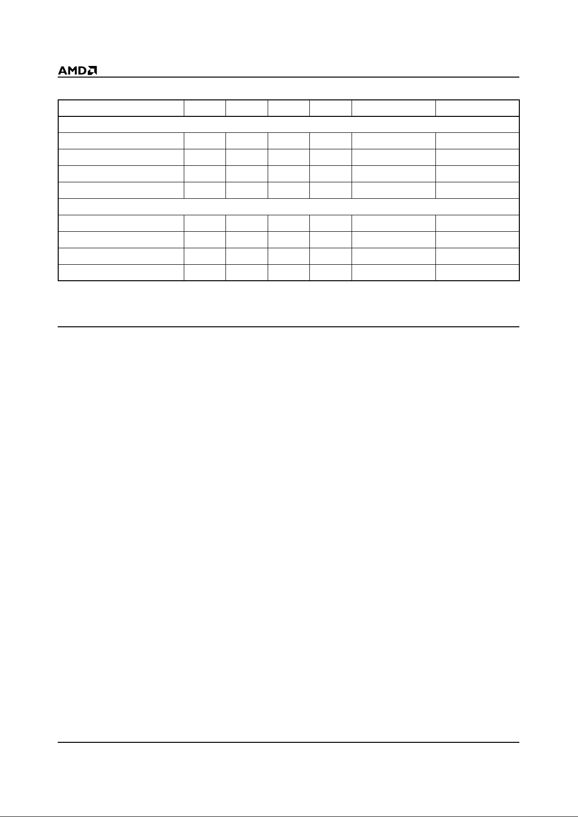
Parameter Symbol Parameter Description Test Conditions Max Unit
C
CARD
Card Input Capacitance 40 pF
C
HOST
System Load Capacitance 120 pF
C
I/O
I/O Capacitance D0–D15 40 pF
Page 26

26 AmMC0XXA
PRELIMINARY
AC CHARACTERISTICS
Read-only Operations
* Not 100% tested.
Parameter Symbol
Parameter Description
Card Speed
Unit
JEDEC Standard -100 -150
t
AVAV
t
RC
Read Cycle Time Min 100 150 ns
t
ELQV
t
CE
Chip Enable Access Time Max 100 150 ns
t
AVQV
t
ACC
Address Access Time Max 100 150 ns
t
GLQV
t
OE
Output Enable Access Time Max 40 50 ns
t
ELQX
t
LZ
Chip Enable to Output in Low-Z Min 0 0 ns
t
EHQZ
t
DF
Chip Disable to Output in High-Z Max 20 30 ns
t
GLQX
t
OLZ
Output Enable to Output in Low-Z Min 0 0 ns
t
GHQZ
t
DF
Output Disable to Output in High-Z Max 20 30 ns
t
AXQX
t
OH
Output Hold from First of Address, CE#, or OE# Change Min 0 0 ns
t
Ready
RESET# Pin Low to Read Mode* Max 20 20 µs
Page 27

AmMC0XXA 27
PRELIMINARY
AC CHARACTERISTICS
Write Operations (Erase/Program)
Parameter Symbols
Parameter Description
Card Speed
UnitJEDEC Standard -100 -150
t
AVAV
t
WC
Write Cycle Time Min 100 150 ns
t
WLWH
t
WP
WE# pulse width Min 45 50 ns
t
ELGL
t
ELWL
CE# setup time to WE# or OE# active Min 0 0 ns
t
AVGL
t
AVWL
Address setup time to WE# or OE# active Min 0 0 ns
t
DVWH
t
DS
Data setup time to WE# inactive Min 45 50 ns
t
WHDX
Data hold time from WE# inactive Min 0 0 ns
t
WHAX
Address hold time from WE# inactive Min 0 0 ns
t
WHEH
CE# hold time from WE# inactive Min 0 0 ns
t
RP
RESET# Pulse Width Min 500 500 ns
t
BUSY
Program/Erase Valid to RY/BY# Delay Min 40 50 ns
t
WHWH1
Programming Operation
Typ 8 8 µs
Max 300 300 µs
t
WHWH2
Sector Erase Operation
Typ 1 1 s
Max 1.5 1.5 s
Page 28

28 AmMC0XXA
PRELIMINARY
KEY TO SWITCHING WAVEFORMS
SWITCHING WAVEFORMS
Figure 7. AC Waveforms for Read Operations
Must be
Steady
May
Change
from H to L
May
Change
from L to H
Does Not
Apply
Don’t Care,
Any Change
Permitted
Will be
Steady
Will be
Changing
from H to L
Will be
Changing
from L to H
Changing,
State
Unknown
Center
Line is HighImpedance
“Off” State
WAVEFORM INPUTS OUTPUTS
KS000010
t
AVAV
t
AVQV
t
AVGL
t
EHQX
OE#
CEL#/CEH#
D0–D15
Valid Data
t
ELGL
t
ELQV
t
ELQNZ
t
GHQZ
t
AXQX
t
GHQX
t
GLQNZ
t
GLQV
A0–A25
20975D-8
Page 29

AmMC0XXA 29
PRELIMINARY
SWITCHING WAVEFORMS
Figure 8. AC Waveforms for Write Operations
Figure 9. AC Waveforms for Data# Polling During Embedded Algorithm Operations
t
AVAV
WE#
CEL#/CEH#
D0–D15
t
DVWH
A0–A25
t
WLWH
t
AVWL
t
WHEH
t
WHAX
t
WHDX
Valid Data
t
ELWL
20975D-9
D0–D7
Valid Data
t
CH
t
OEH
t
OE
t
CE
t
WHWH1 or tWHWH2
D7=
Valid Data
High Z
CE#
OE#
WE#
t
OH
D7#
D0–D6=Invalid
*D7=Valid Data (The device has completed the Embedded operation).
*
20975D-10
D0–D6
t
DF
D7
Page 30

30 AmMC0XXA
PRELIMINARY
SWITCHING WAVEFORMS
Figure 10. RY/BY# Timing Diagram During Program/Erase Operations
Figure 11. RESET# Timing Diagram
CE#
WE#
RY/BY#
t
BUSY
Entire programming
or erase operations
The rising edge of the last WE# signal
20975D-11
RESET#
20975D-12
t
Ready
t
RP
Page 31

AmMC0XXA 31
PRELIMINARY
AC CHARACTERISTICS—ALTERNATE CE# CONTROLLED WRITES
Write/Erase/Program Operations
Notes:
1. Rise/fall time
≤
10 ns.
2. Card Enable Controlled Programming:
Flash Programming is controlled by the valid combination of the Card Enable (CE1#, CE2#) and Write Enable (WE#) signals.
For systems that use the Card Enable signal(s) to define the write pulse width, all setup, hold, and inactive write enable timing
should be measured relative to the Card Enable signal(s).
Parameter Symbols
Parameter Description
Card Speed
UnitJEDEC Standard -100 -150
t
AVAV
t
WC
Write Cycle Time Min 100 150 ns
t
AVEL
t
AS
Address Setup Time Min 10 10 ns
t
ELAX
t
AH
Address Hold Time Min 45 50 ns
t
DVEH
t
DS
Data Setup Time Min 45 50 ns
t
EHDX
t
DH
Data Hold Time Min 20 20 ns
t
GLDV
t
OEH
Output Enable Hold Time for Embedded Algorithm Min 10 10 ns
t
GHEL
Read Recovery Time before Write Min 0 0 µs
t
WLEL
t
WS
WE# Setup Time before CE# Min 0 0 ns
t
EHWH
t
WH
WE# Hold Time Min 0 0 ns
t
ELEH
t
CP
CE# Pulse Width Min 45 50 ns
t
EHEL
t
CPH
CE# Pulse Width HIGH (Note 2) Min 20 20 ns
t
EHEH3
Embedded Programming Operation (Notes 2)
Typ 8 8 µs
Max 300 300 µs
t
EHEH4
Embedded Erase Operation for each 64K byte
Memory Sector (Notes 1)
Typ 1 1 s
Max 1.5 1.5 s
t
VCS
VCC Setup Time to Write Enable LOW Min 50 50 µs
Page 32

32 AmMC0XXA
PRELIMINARY
Notes:
1. PA is address of the memory location to be programmed.
2. PD is data to be programmed at byte address.
3. DQ7 is the complement of the data written to the device.
4. D
OUT
is the data written to the device.
5. Figure indicates last two bus cycles of four bus cycle sequence.
6. Waveforms are for the x16 mode.
20975D-13
Figure 12. Alternate CE# Controlled Write Operation Timings
t
WH
t
WS
OE#
CE#
WE#
V
CC
t
DS
Data
t
AH
Addresses
t
DH
t
CP
PD
DQ7# D
OUT
t
EHEH3_or_4
t
WC
t
AS
t
CPH
t
VCS
XXXXh
PA PA
Data# Polling
A0h
t
GHEL
Page 33

AmMC0XXA 33
PRELIMINARY
AIS MEMORY MAP
The AIS (Attribute Information Structure) is an area of
memory used for storing information about the configuration of the Miniature Card. The AIS is recommended
to be stored in the first sector of the first device of the
Flash array. As this area is not explicitly protected, the
AIS information must be reloaded onto the card in the
event that the information is erased.
The AIS has five unique information areas:
1. Identification Data: This data includes Manufacturer
information (Manufacturer and card name).
2. Compatibility Data: This data specifies basic information about the card (memory size, access time,
memory type, power, etc.)
3. Burst Data (not applicable)
4. DRAM Data (not applicable)
5. Reserved Data: This data ar ea is reserved for future
use.
The AIS supports up to four different memory technologies on a card. Some of the information areas are
repeated in the memory ma p in order to specify different technologies (see Ta ble 16). The Technology
Count field in the Identification Data section defines the
number of different technologies on a card. The first
memory technology is defined in the AIS memory map
from address 40h thr ough 7Fh. The second memory
technology is defined from 80h through BFh. The third
memory technology is defined from C0h to DFh. The
fourth memory technology is defined from E0h to FFh.
The AIS is stored as bytes within the 16-bit Miniature
Card data word. The even byte D0–D7 stores the AIS
data, and the odd byte D8–D15 is reserved by the card
manufacturer for manufacturing information.
Table 16. Miniature Card AIS Memory Assignments
* For more information on PC Card Compatibility refer to Table 17 or the Miniature Card PC Compatibility Guide.
Note: “Not applicable” indicates the address space does not apply to AMD Flash Miniature Cards, but is defined by MCIF.
Card Address Section Description
00h–0Fh PC Card Compatibility Area* Reserved for PC Card Tuples
10h–1Fh Identification Data Identifies Card Type
20h–2Fh Identification Data Identifies Card Type
30h–3Fh Identification Data Identifies Card Type
40h–4Fh Compatibility Data (Area 1) Memory Technology #1
50h–5Fh Burst Data (not applicable)
60h–6Fh DRAM Data (not app lica ble)
70h–7Fh Reser ved for future use
80h–8Fh Compatibility Data (not applicable) (Memory Technology #2)
90h–9Fh Burst Data (not applicable)
A0h–AFh DRAM Data (not applicable)
B0h–BFh Reserved for future use
C0h–CFh Compatibility Data (not applicable) (Memory Technology #3)
D0h–DFh Reser ved for future use
E0h–EFh Compatibility Data (not applicable) (Memory Technology #4)
F0h–FFh Reserved for future use
Page 34

34 AmMC0XXA
PRELIMINARY
Table 17. PC Card Compatibility Memory Assignments
Address Values Description
00h 01h TPL_CODE CISTPL_DEVICE
01h 03h TPL_LINK
02h 53 Device ID
03h 2MB = 7C, 4MB = FC; 8MB = 1E Device Size
04h FF End of CISTPL_DEVICE
05h 00h CISTPL_NULL
06h 00h CISTPL_NULL
07h 00h CISTPL_NULL
08h 00h CISTPL_NULL
09h 00h CISTPL_NULL
0Ah 00h CISTPL_NULL
0Bh 00h CISTPL_NULL
0Ch 00h CISTPL_NULL
0Dh 00h CISTPL_NULL
0Eh 80h TPL_CODE CISTPL_MINI
0Fh F0h TPL_LINK
Page 35

AmMC0XXA 35
PRELIMINARY
Identification Data
The Identificatio n Data provides basic identi fication
information about the card. This data section is
required on all cards. Table 18 shows the Identification
Data for AMD’s 5 v olt-only Miniature cards.
Compatibility Data
The compatibil ity data provides basic compatib ility
across all cards. This data section is required on all
cards. The addresses i n parentheses are specified f or
cards with more than one memory technology on the
card. Table 19 shows the compatibility data for AMD
5-volt only Miniature Cards.
Table 18. AMD Identification Data
Card Address Value Description
10h 99h
Miniature Card Identifier: Fixed value for a host to identify an inserted
Miniature Card
11h 11h
Level of Compliance: Defines the level of AIS supported. The
Miniature Cards described in this document are rev 1.1 compliant.
12h 01h or FDh or F9h
AIS Checksum: Th e modul o-256 s um of al l e v en b yt es fr om 10h–F Fh.
A valid checksum sums to 00h (2’s complement).
2 Mbyte card: 99h + 01h = 00h
4 Mbyte card: 03h + FDh = 00h
8 Mbyte card: 07h + F9h = 00h
13h 41h
Manufacturer Name: 13h–26h. String of ASCII characters at
addresses 13h to 26h to identify the manufacturer of the Miniature
Card.
ASCII character “A”
14h 4Dh ASCII character “M”
15h 44h ASCII character “D”
16h 20h ASCII character - SPACE
17h 49h ASCII character - “I”
18h 4Eh ASCII character - “N”
19h 43h ASCII character - “C”
1Ah 00h ASCII character - NULL
1Bh 00h ASCII character - NULL
1Ch–26h 00h Unused space in manufacturer name field
27h 35h
Card Name: (addresses 27h–3Ah). String of ASCII characters to
identify the card name.
ASCII character “5”
28h 56h ASCII character “V”
29h 4Dh ASCII character “M”
2Ah 43h ASCII character “C”
2Bh 20h ASCII character - SPACE
2Ch 53h ASCII character “S”
2Dh 65h ASCII character “e”
2Eh 72h ASCII character “r”
2Fh 69h ASCII character “i”
30h 65h ASCII character “e”
31h 73h ASCII character “s”
Page 36

36 AmMC0XXA
PRELIMINARY
Note: All reserved bytes must be set to 00h. All reserved fields (bits) within bytes must be set to 0 (binary). All unused fields must
be set to 00h.
32h 00h ASCII character - NULL
33h–3Ah 00h Unused space in card name field
3Bh 01h
Technology Count: Defines the number of different memory
technologies on the Miniature Card.
Technology count set to 1
3Ch–3Fh 00h Reserved space set to 00h; for future use
Table 18. AMD Identification Data (Continued)
Card Address Value Description
Table 19. AMD Compatibility Data
Card Address Value Description
40h 00h Defines the type of memory technology; Flash = 000 binary
41h 01h Device JEDEC Manufacturer ID
42h D5h or 3Dh Device JEDEC Component ID: Am29F080B = D5h, Am29F017B = 3Dh
43h 01h or 03h or 07h Memory array size: 01 = 2 Mbyte, 03 = 4 Mbyte, 07 = 8 Mbyte
44h 00h N/A
45h 00h N/A
46h 0Ah 5.0 Volt Access Time: 100 ns
47h 00h N/A
48h 00h N/A
49h 8Ch
Typical read/write current at 5.0 Volts (word mode): 80mA read, 120 mA
write
4Ah 0Ah Typical standby current: 1 mA
4Bh–4Fh, 8Ch–8Fh,
CCh–CFh, ECh–EFh
00h Reserved for future use
80h–8Bh, C0–CBh,
E0h–EBh
00h
These addresses are designated for other memory technologies, which
are not used in AMD Flash Miniature Cards.
100h 18h TPL_CODE CIS TP L_J ED EC _C
101h 02h TPL_LINK
102h 01h Manufacturer ID
103h D5 = 2M; 3D = 4M,8M
Device ID
2Mbyte card: D5
4Mbyte card: 3D
8Mbyte card: 3D
104h 1Eh TPL_CODE CISTPL_D EV ICE GE O
105h 06h TPL_LINK
106h 02h DGTPL_BUS: Bus Width
107h 01h DGTPL_EBS:11h = 64K Byte Erase Block size
108h 01h DGTPL_RBS: Read Byte Size
109h 01h DGTPL_WBS: Write Byte Size
10Ah 01h DGTPL_PART: Number of partition
10Bh 01h FL DEVICE INTERLEAVE: No interleave.
Page 37

AmMC0XXA 37
PRELIMINARY
PHYSICAL DIMENSIONS
Top View
38.00 mm
1.496 in.
33.00 mm
1.299 in.
.118 in.
3.00 mm
.150 in.
3.81 mm
.118 in.
3.00 mm
.118 in.
3.00 mm
.118 in.
3.212 mm
.217 in.
5.50 mm
.217 in.
5.50 mm
.161 in.
4.09 mm
center line
.244 in.
6.21 mm
Page 38

38 AmMC0XXA
PRELIMINARY
PHYSICAL DIMENSIONS
Bottom View
Right Side View
Write Protect Switch Location
0.245
0.600
Write Protect Switch Location
0.245
Page 39

AmMC0XXA 39
PRELIMINARY
REVISION SUMMARY FOR AMMC0XXA
Global
Changed all Am29F016 references to Am29F017B.
Added -100 (100 ns) speed option and specifications.
Distinctive Characteristics
Revised low power consumption specifications. Added indus-
trial temperature range bullet. Deleted “Small Form Factor”
bullets. Revised text to indicate that the Miniature Card specification will be defined by PCMCIA.
General Description
Deleted references to the elastomeric connector.
Table 1, Miniature Card Definitions
Deleted references to the elastomeric connector.
Ordering Information
Added indus trial tem perature range. Ad ded Valid Combinations table. Deleted NP optio n from part number. Added WP
as part of required base part number.
Figure 2, Host/Card Address Connections
Clarified drawing by designating host bus and card bus.
Added A21 address pin. Redesignated NC connections.
Miniature Card Pad Assignments
BUSY#: Revised to indica te that the Miniat ure Card cannot
accept most operations when BUSY# is low. CD#: Deleted
last sentence.
Sector Group Protection
Added section.
Tables 5–9, Command Definitions
Revised for easier reference: removed “H” d esignators from
table (now indicated in notes ), rem oved 4-cycle Reset/Re ad
command, sep arated Read and R eset comman ds, moved
RA, RW, RD, PA, PW, PD, X, SA definitions to legend. Moved
Erase Suspend and Erase Resume defin itions from table to
notes.
Table 12, Memory Sector Addresses for 4 and 8
Mbyte Cards
Added Note 3 to include 8 Mbyte cards.
Embedded Erase Algorithm
Removed last paragraph.
Absolute Maximum Ratings
Revised storage and ambient temperature ratings.
Operating Ranges
Added industrial tem perat ure range.
DC Characteristics
Revised ICC specifications. Added frequenc y specifi cation to
Note 2.
AC Characteristics, Write (Erase/Program)
Operations
Deleted t
ELQV
, t
AVQ V
, t
GLQV
, t
ELQX
, t
EHOZ
, t
GLOX
, t
GHQZ
,
t
AXQ
X, t
WHGL
, t
GLQNZ
.
Table 19, AMD Compatibility Data
Added two tuples of data to list, coverin g addresses 10 0h–
10Bh. Changed a ddress 46h data to 0Ah, correspond ing to
an access time of 100 ns.
Revision D+1
Sector Erase Suspend
Removed the statement requiring the address of a sector not
being erased to obtain valid D6 status.
Trademarks
Copyright © 1998 Advanced Micro Devices, Inc. All rights reserved.
AMD, the AMD logo, and combinations thereof are trademarks of Advanced Micro Devices, Inc.
Product names used in this publication are for identification purposes only and may be trademarks of their respective companies.
 Loading...