

Datasheet AMC020DFLKACS, AMC008DFLKACS, AMC004DFLKACS, AMC032DFLKACS Datasheet (AMD Advanced Micro Devices)
Page 1

FINAL
Publication# 19521 Rev: D Amendment/0
Issue Date: December 1996
AmC0XXDFLKA
4, 8, 20, or 32 Megabyte 5.0 Volt-only Flash Memory PC Card
DISTINCTIVE CHARACTERISTICS
■
High performance
— 150 ns maximum access time
■
Single supply operation
— Write and erase voltage, 5.0 V ± 5%
— Read voltage, 5.0 V ± 5%
■
CMOS low power consumption
— 45 mA maximum active read current (x8 mode)
— 65 mA maximum active write/erase current
(x8 mode)
■
High write endurance
— Minimum 100,000 program/erase cycles per
sector
— 1,000,000 typical program/erase cycles per card
■
PCMCIA/JEIDA 68-pin standard
— Selectable byte-/or word-wide configuration
■
Write protect switch
— Prevents accidental data loss
■
Zero data retention power
— Batteries not required for data storage
■
Enhanced power management for standby
mode
—1 µ A typical standby current
— Standard access time from standby mode
■
Separate attribute memory
■
Automated write and erase operations increase
system write performance
— 64K byte memory sectors for faster automated
erase speed
— Typically 1 s per single memory sector erase
— Random address writes to previously erased
bytes (8 µ s typical per byte)
■
Total system integration solution
— Support from independent software and
hardware vendors
■
Low insertion and removal force
— State-of-the-art connector allows for minimum
card insertion and removal effort
■
Erase Suspend/Resume
— Supports reading or programming data to a
sector not being erased within the same device
■
Support for RY/BY
and RESET signals
GENERAL DESCRIPTION
AMD’s 5.0 Volt-only Flash Memory PC Card provides
the highest system level performance for data and file
storage solutions to the portable PC market segment
and a wide range of embedded applications. Manufactured with AMD’s Negative Gate Erase, 5.0 Volt-only
technology, the AMD 5.0 Volt-only Flash Memory
Cards are the most cost-effective and reliable approach to single-supply Flash memory cards. Data files
and application programs can be stored on the D-Series cards. This allows OEM manufacturers of portable
systems to eliminate the weight, high-power consumption and reliability issues associated with
electro-mechanical disk-based systems. The D-Series
cards also allow today’ s b ulky and hea vy battery packs
to be reduced in weight and size. AMD’ s Flash Memory
PC Cards provide the most efficient method to transfer
useful work between different hardware platforms. The
enabling technology of the D-Series cards enhances
the productivity of mobile workers.
Widespread acceptance of the D-Series cards
is assured due to their compatibility with the
68-pin PCMCIA/JEIDA international standard. AMD’s
Flash Memory Cards can be read in either a byte-wide
or word-wide mode which allows for flexible integration
into various system platforms. Compatibility is assured
at the hardware interface and software interchange
specification. The Card Information Structure (CIS) or
Metaformat, can be written by the OEM into the memory card’s attribute memory address space beginning
at address 00000H by using a format utility. The CIS
appears at the beginning of the Card’s attribute memory space and defines the low-level organization of
data on the PC Card. The D-Series cards contains a
separate EEPROM memory for the cards’ attribute
memory space. This allows all of the Flash memory to
be used for the common memory space.
Third party software solutions such as Microsoft’s and
SystemSoft’s Flash File System (FFS2), SCM’s
SCM-FTL, and Datalight’s Cardtrick enable AMD’s
Flash Memory PC Card to replicate the function
of traditional disk-based memory systems.
Page 2
2 AmC0XXDFLKA
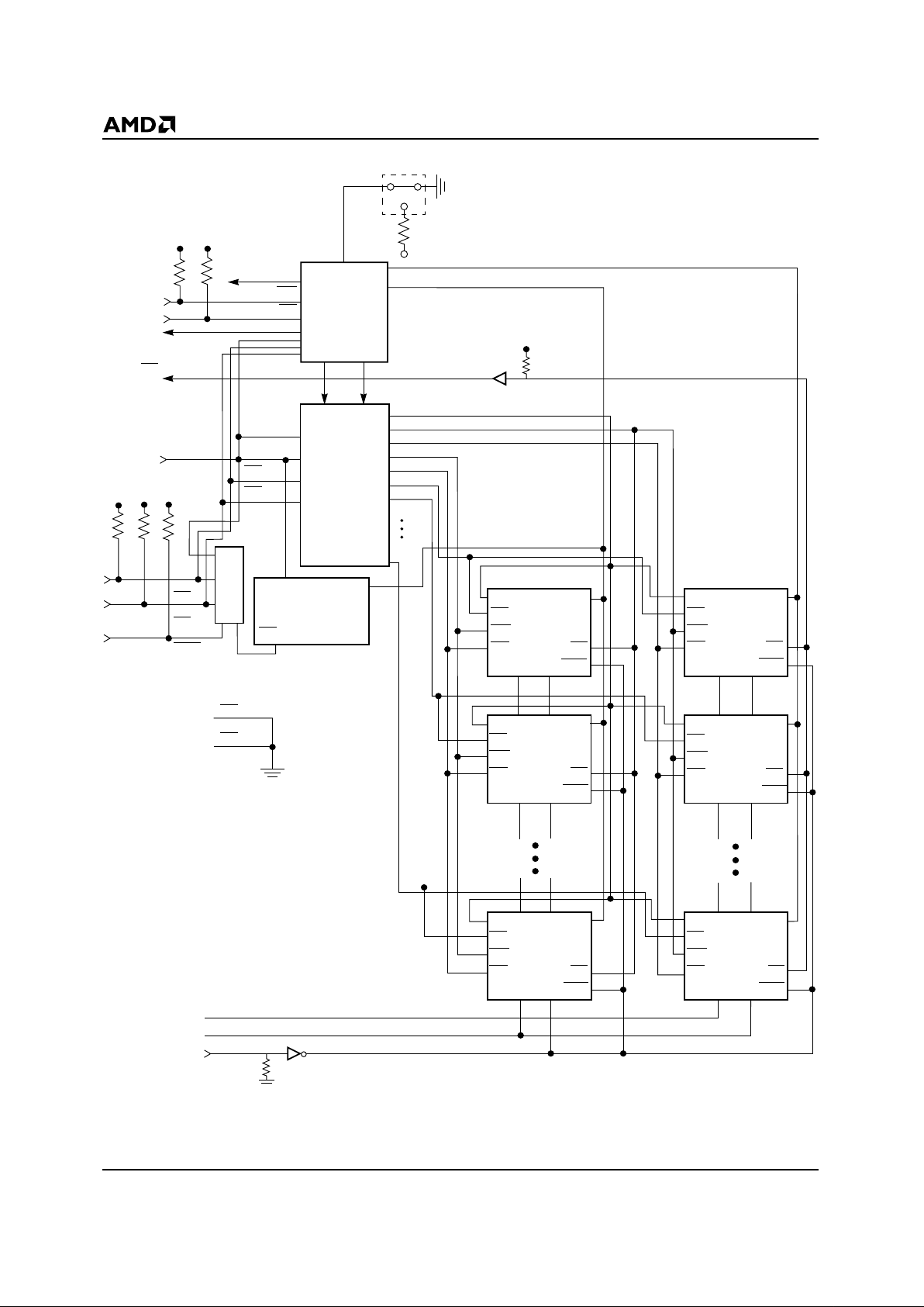
BLOCK DIAGRAM
Notes:
R = 20 K(min)/140 K
Ω
(max)
*4 Mbyte card = S0 + S1, 8 Mbyte card = S0…S3, 20 Mbyte card = S0…S9, 32 Mbyte card = S0…S15
Address
Buffers
and
Decoders
I/O
Transceivers
and
Buffers
A0–A8 D0–D7
Attribute Memory
CE
Write Protect Switch
V
CC
D0–D15
WE
OE
D8–D15
D0–D7
A0
A1–A24
CE
2
CE
1
A1–A9
A0
CE
2
CE1
REG
CD1
CD
2
Card Detect
GND
V
CC
R
R
Decoder
V
CC
RR
Am29F016C
A0–A20 D0–D7
CE
WE
OE RY/BY
V
SS VCC
RST
S0*
Am29F016C
A0–A20 D8–D15
CE
WE
OE RY/BY
V
SS VCC
RST
S1*
A0–A20 D0–D7
CE
WE
OE RY/BY
V
SS VCC
RST
S2*
A0–A20 D8–D15
CE
WE
OE RY/BY
V
SS VCC
RST
S3*
A0–A20 D0–D7
CE
WE
OE RY/BY
V
SS VCC
RST
S14*
A0–A20 D8–D15
CE
WE
OE RY/BY
V
SS VCC
RST
S15*
19521D-1
WP
10K
10K
A0–A24
ICE7
ICE0
ICE1
IOEL
IWEL
IOEH
IWEH
A1-A21
V
CC
RESET
RY/BY
(Output)
R
V
CC
3.3K
Page 3
AmC0XXDFLKA 3
PC CARD PIN ASSIGNMENTS
Notes:
I = Input to card, O = Output from card
I/O = Bidirectional
NC = No connect
In systems which switch V
CC
individually to cards, no signal should be directly connected between cards other than ground.
1. V
PP
not required for Programming or Reading operations.
2. BVD
= Internally pulled-up.
3. Signal must not be connected between cards.
Pin# Signal I/O Function Pin# Signal I/O Function
1 GND Ground 35 GND Ground
2 D3 I/O Data Bit 3 36 CD1 O Card Detect 1 (Note 3)
3 D4 I/O Data Bit 4 37 D11 I/O Data Bit 11
4 D5 I/O Data Bit 5 38 D12 I/O Data Bit 12
5 D6 I/O Data Bit 6 39 D13 I/O Data Bit 13
6 D7 I/O Data Bit 7 40 D14 I/O Data Bit 14
7CE
1 I Card Enable 1 (Note 3) 41 D15 I/O Data Bit 15
8 A10 I Address Bit 10 42 CE
2 I Card Enable 2 (Note 3)
9OE
I Output Enable 43 NC No Connect
10 A11 I Address Bit 11 44 NC No Connect
11 A9 I Address Bit 9 45 NC No Connect
12 A8 I Address Bit 8 46 A17 I Address Bit 17
13 A13 I Address Bit 13 47 A18 I Address Bit 18
14 A14 I Address Bit 14 48 A19 I Address Bit 19
15 WE
I Write Enable 49 A20 I Address Bit 20
16 RY/BY
Ready/Busy 50 A21 I Address Bit 21
17 V
CC1
Power Supply 51 V
CC2
Power Supply
18 NC No Connect (Note 1) 52 NC No Connect (Note 1)
19 A16 I Address Bit 16 53 A22 I Address Bit 22
20 A15 I Address Bit 15 54 A23 I Address Bit 23
21 A12 I Address Bit 12 55 A24 I Address Bit 24
22 A7 I Address Bit 7 56 NC No Connect
23 A6 I Address Bit 6 57 NC No Connect
24 A5 I Address Bit 5 58 RESET RESET
25 A4 I Address Bit 4 59 NC No Connect
26 A3 I Address Bit 3 60 NC No Connect
27 A2 I Address Bit 2 61 REG
I Register Select
28 A1 I Address Bit 1 62 BVD
2 O Battery Vltg Detect 2 (Note 2)
29 A0 I Address Bit 0 63 BVD
1 O Battery Vltg Detect 1 (Note 2)
30 D0 I/O Data Bit 0 64 D8 I/O Data Bit 8
31 D1 I/O Data Bit 1 65 D9 I/O Data Bit 9
32 D2 I/O Data Bit 2 66 D10 I/O Data Bit 10
33 WP O Write Protect (Note 3) 67 CD
2 O Card Detect 2 (Note 3)
34 GND Ground 68 GND Ground
Page 4

4 AmC0XXDFLKA
ORDERING INFORMATION
Standard Products
AMD standard products are available in se ver al packages and operating r anges. The order number (Valid Combination) is formed
by a combination of:
OUTPUT CONFIGURATION:
(x16/x8)
FLASH TECHNOLOGY
PC MEMORY CARD
MEMORY CARD DENSITY
004 = Four Megabytes
008 = Eight Megabytes
020 = Twenty Megabytes
032 = Thirty-two Megabytes
AMD
REVISION LEVEL
5.0 V olt-only OPERATION
WITH 100,000 ERASE/PROGRAM
CYCLES MINIMUM
AM C 0XX D FL
K
A
CSxxxxx
CUSTOMER SPECIFIC
IDENTIFICATION NUMBER
Page 5

AmC0XXDFLKA 5
Differences Between the D-Series and
C-Series Cards
The differences between the D-Series Card and the
earlier C-Series Cards are as follows:
■
The D-Series Cards are based on AMD’s latest 16
MBit 5.0 Volt-only device, the Am29F016C . The earlier C-Series Cards were based on the 4 MBit 5.0
Volt-only device, the Am29F040.
■
The D-Series Cards program faster than the CSeries Cards. This is due to faster byte write times
and an optimized address unlock sequence for
write operations.
■
The D-Series Cards are offered in higher densities. The D-Series Cards are available in densities
of 4 MBytes, 8 MBytes, 20 MBytes, and 32
MBytes. The earlier C-Series Cards were available in densities of 1 MByte, 2 MBytes, 4 MBytes
and 10 MBytes.
The additional features that are supported in the new
D-Series Cards include
■
The D-Series Cards support the RESET feature.
This allows you to asynchronously RESET the Card
into the read state.
■
The D-Series Cards also provide the RY/BY
functionality. This feature provides a quick way of determining if the Card is busy doing a write or erase
operation, or if it is in a position to undertake the
next operation.
■
Availability of an additional Toggle bit (D2) to determine if the Card is in the Embedded Erase or Erase
Suspend mode.
■
Programming operations can be executed in 8 µ s
pulses, down from the 16 µ s on the C-Series
Cards (typical).
■
Time out from the rising edge of the WE
pulse for
sector erase command reduced from 100 µ s to
50 µ s.
■
The D-Series Cards offers a low power standby
mode with fast recovery time to read. The typical
standby current (I
CCS
) is <1 µ A with recovery at
standard read access time.
Page 6

6 AmC0XXDFLKA
PIN DESCRIPTION
A0–A24
Address Inputs
These inputs are internally latched during write cycles.
All address lines should be driven.
BVD1, BVD2
Battery V oltage Detect
Internally pulled-up.
CD1, CD2
Card Detect
When card detect 1 and 2 = ground the system detects
the card.
CE1, CE2
Card Enable
This input is active low . The memory card is deselected
and power consumption is reduced to standby levels
when CE
is high. CE activates the internal memor y
card circuitry that controls the high and low byte control
logic of the card, input buffers segment decoders, and
associated memory devices.
D0–D15
Data Input/Output
Data inputs are internally latched on write cycles. Data
outputs during read cycles. Data pins are active high.
When the memory card is deselected or the outputs
are disabled the outputs float to tristate.
GND
Ground
NC
No Connect
Corresponding pin is not connected.
OE
Output Enable
This input is active low and enables the data buffers
through the card outputs during read cycles.
RY/BY
This signal is output from the card and indicates the
status of the operation in progress in the card. If this
signal is low, then the card is still busy with the current
operation. Otherwise, the card is ready to accept anew
operation.
REG
Attribute Memory Select
This input is active low and enables reading the CIS
from the EEPROM.
RESET
This input to the Card is used to reset all the Flash devices inside the Card to a read mode state. If you drive
or assert RESET high during a write or erase operation, then the state of the devices for the purpose of the
operation is undefined. In order to RESET, you need to
hold the RESET pin high for 500 ns, and it takes 20 µ s
before the internal circuit is RESET. When RESET is
driven high, the data bus is in a high impedance state.
V
CC
PC Card Power Supply
For device operation (5.0 V ± 5%).
WE
Write Enable
This input is active low and controls the write function
of the command register to the memory array. The
target address is latched on the falling edge of the WE
pulse and the appropriate data is latched on the rising
edge of the pulse.
WP
Write Protect
This output is active high and disables all Card write
operations (including writes to the attribute memory).
MEMORY CARD OPERATIONS
The D-Series Flash Memory Card is organized as an
array of individual devices. Each device is 2 Mbytes in
size with thirty-two 64K byte sectors. Although the address space is continuous, each physical device defines a logical address segment size.
Erase operations can be performed on two 64KByte
sectors simultaneously. Once a memory sector or
memory segment is erased any address location may
be programmed. Flash technology allows any logical
“1” data bit to be programmed to a logical “0”. The
only way to reset bits to a logical “1” is to erase the
entire memory sector of 64K bytes or memory segment of 2 Mbytes.
Erase operations are the only operations that work on
entire memory sectors or memory segments. All other
operations such as word-wide programming are not affected by the physical memory segments.
The common memory space data contents are altered
in a similar manner as writing to individual Flash memory devices. On-card address and data buffers activate
the appropriate Flash device in the memory array.
Each device internally latches address and data during
write cycles. Refer to Table 1.
Attribute memory is a separately accessed card memory space. The attribute memory space is active when
the REG
pin is driven low. The Card Information Struc-
ture (CIS) describes the capabilities and specification
Page 7
AmC0XXDFLKA 7
of a card. The CIS is stored in the attribute memory
space beginning at address 00000H. The D-Series
cards contain a separate EEPROM for the Card Information Structure. D0–D7 are active during attribute
memory accesses. D8–D15 should be ignored. Odd order bytes present invalid data. Refer to Table 2.
Word-Wide Operations
The D-Series cards provide the flexibility to operate on
data in a byte-wide or word-wide format. In word-wide
operations the CE
1 and CE2 must be low and A0 is not
used for any addressing.
Table 1. Common Memory Bus Operations
Notes:
1. X indicates a don’t care value.
2. V
PP
pins are not connected in the 5.0 Volt-only Flash Memory Card.
3. Refer to Table 5 for valid D
IN
during a word write operation.
4. Refer to Table 3 and 4 for valid D
IN
during a byte write operation.
5. During odd byte access, A0 = V
IH
outputs or inputs the “odd” b yte (high byte) of the x16 word on D0–D7. This is accomplished
internal to the card by transposing D8–D15 to D0–D7.
6. During odd-byte-only access , A0 = X outputs or inputs the “odd” byte (high byte) of the x16 word on D8–D15.
Function REG CE2CE1OEWE A0 D8–D15 D0–D7
Read Mode
Standby Mode X H H X X X High-Z High-Z
Word Access H L L L H X Data Out-Odd Data Out-Even
Low Byte Access H H L L H L High-Z Data Out-Even
Odd Byte Access H H L L H H High-Z Data Out-Odd
Odd-Byte-Only Access HLHLHXData Out-Odd High-Z
Write Mode
Standby Mode X H H X X X X X
Word Access (Note 3)
H
L L H L X Data In-Odd Data In-Even
Even Byte Access (Note 4) H HLHLL High-Z Data In-Even
Odd Byte Access (Note 4) H HLHLH High-Z Data In-Odd
Odd-Byte-Only Access (Note 4) H L H H L X Data In-Odd High-Z
Output Disable H X X H H X High-Z High-Z
Page 8
8 AmC0XXDFLKA
Table 2. Attribute Memory Bus Operations
Notes:
1. X indicates any value.
2. V
PP
pins are not connected in the 5.0 Volt-Only Flash Memory Card.
3. During Attribute Memory Read function, REG
and OE must be active for the entire cycle.
4. Only even-byte data is valid during Attribute Memory Read function.
5. During Attribute Memory Write function, REG
and WE must be active for the entire cycle, OE must be inactive for the
entire cycle.
6. The first 128 bytes of the attribute memory is not writable as it contains the CIS. Only the remaining 384 bytes are writable.
Pins/Operation REG CE2CE1OEWE A0 D8–D15 D0–D7
READ/WRITE
Read Mode (Note 3)
Standby Mode X H H X X X High-Z High-Z
Word Access (Note 4) LLLLHX Not Valid Data Out-Even
Even Byte Access L H L L H L High-Z Data Out-Even
Odd Byte Access (Note 4) L H L L H H High-Z Not Valid
Odd-Byte-Only Access (Note 4) L LHLHX Not Valid High-Z
Write Mode (Note 5,6)
Standby Mode X H H X X X X X
Word Access L L L H L X X Data In-Even
Low Byte Access LHLHLL X Data In-Even
Odd Byte Access LHLHLH X X
Odd-Byte-Only Access L L H X H L X X
Output Disable L X X H H X High-Z High-Z
Page 9

AmC0XXDFLKA 9
Byte-Wide Operations
Byte-wide data is available on D0–D7 f or read and write
operations (CE1 = low, CE2 = high). Even and odd
bytes are stored in separate memory segments (i.e.,
S0 and S1) and are accessed when A0 is low and high
respectively. The even byte is the low order byte and
the odd byte is the high order byte of a 16-bit word.
Erase operations in the byte-wide mode must account
for data multiplexing on D0–D7 b y changing the state of
A0. Each memory sector or memor y segment pair
must be addressed separately for erase operations.
Card Detection
Each CD (output) pin should be read by the host system to determine if the memory card is adequately
seated in the socket. CD1 and CD2 are internally tied
to ground. If both bits are not detected, the system
should indicate that the card must be reinserted.
Write Protection
The AMD Flash memory card has three types of write
protection. The PCMCIA/JEIDA socket itself provides
the first type of write protection. P o wer supply and control pins have specific pin lengths in order to protect the
card with proper power supply sequencing in the case
of hot insertion and removal.
A mechanical write protect switch provides a second
type of write protection. When this switch is activated,
WE is internally forced high. The Flash memory command register is disabled from accepting any write
commands.
The third type of write protection is achieved with V
CC1
and V
CC2
below 3.2 V V
LKO
. Each Flash memory device that comprises a Flash memory segment will
reset the command register to the read-only mode
when VCC is below V
LKO
. V
LKO
is the voltage below
which write operations to individual command registers are disabled.
MEMORY CARD BUS OPERATIONS
Read Enable
Two Card Enable (CE) pins are available on the memory card. Both CE pins must be active low for
word-wide read accesses. Only one CE is required for
byte-wide accesses. The CE pins control the selection
and gates power to the high and low memory segments. The Output Enable (OE) controls gating accessed data from the memory segment outputs.
The device will automatically power-up in the read/
reset state. In this case, a command sequence is not
required to read data. Standard microprocessor read
cycles will retrieve array data. This default value ensures that no spurious alteration of the memory content
occurs during the power transition. Refer to the AC
Read Characteristics and Waveforms for the specific
timing parameters.
Output Disable
Data outputs from the card are disabled when OE is at
a logic-high level. Under this condition, outputs are in
the high-impedance state.
Standby Operations
Byte-wide read accesses only require half of the read/
write output buffer (x16) to be active. In addition, only
one memory segment is active within either the high
order or low order bank. Activation of the appropriate
half of the output buffer is controlled by the combination
of both CE
pins. The CE pins also control power to the
high and low-order banks of memory. Outputs of the
memory bank not selected are placed in the high impedance state. The individual memory segment is activated by the address decoders. The other memory
segments operate in standby. An active memory segment continues to draw power until completion of a
write or erase operation if the card is deselected in the
process of one of these operations.
Auto Select Operation
A host system or external card reader/writer can determine the on-card manufacturer and device I.D. codes.
Codes are available after writing the 90H command to
the command register of a memory segment per
Tables 3 and 4. Reading from address location 00000H
in any segment provides the manufacturer I.D. while
address location 00002H provides the device I.D.
To terminate the Auto Select operation, it is necessary to write the Read/Reset command sequence
into the register.
Write Operations
Write and erase operations are valid only when V
CC1
and V
CC2
are above 4.75 V. This activ ates the state machine of an addressed memory segment. The command register is a latch which saves address,
commands, and data information used by the state machine and memory array.
When Write Enable (WE) and appropriate CE(s) are at
a logic-level low, and Output Enable (OE) is at a
logic-high, the command register is enabled for write
operations. The falling edge of WE latches address information and the rising edge latches data/command
information.
Write or erase operations are performed by writing appropriate data patterns to the command register of accessed Flash memory sectors or memory segments.
The byte-wide and word-wide commands are defined
in Tables 3, 4, and 5, respectively.
Page 10
10 AmC0XXDFLKA
Table 3. Even Byte Command Definitions (Note 5)
* Address for Memory Segment 0 (S0) only. Address f or the higher ev en memory segments (S2–S14) = (Addr) + (N/2)* 400000H
where N = Memory Segment number (0) for 4 Mbyte, N = (0, 2) for 8 Mb yte, N = (0, 2, 4) f or 12 Mbyte , N = (0…8) f or 20 Mbyte,
N = (0...14) for 32 Mbyte.
Notes:
1. Address bits = X = Don’t Care for all address commands except for Program Address (PA), Read Address (RA) and Sector
Address (SA).
2. Bus operations are defined in Table 1.
3. RA = Address of the memory location to be read.
PA = Address of the memory location to be programmed. Addresses are latched on the falling edge of the WE
pulse.
SA = Address of the sector to be erased. The combination of A17, A18, A19, A20, A21 will uniquely select any sector of a
segment.
To select the memory segment: 4 Mbyte: Use CE
1
8 Mbyte: Use CE
1 and A22
20 and 32 Mbyte: Use CE
1 and A22-A24.
4. RD = Data read from location RA during read operation.
PD = Data to be programmed at location PA. Data is latched on the rising edge of WE
pulse.
5. A0 = 0 and CE
1 = 0.
Embedded
Command
Sequence
Bus
Write
Cycles
Req’d
First Bus
Write Cycle
Second Bus
Write Cycle
Third Bus
Write Cycle
Fourth Bus
Read/Write Cycle
Fifth Bus
Write Cycle
Sixth Bus
Write Cycle
Addr* Data Addr* Data Addr* Data Addr* Data Addr* Data Addr* Data
Reset/Read 1 XXXXH F0
Reset/Read 4 XXXXH AA XXXXH 55 XXXXH F0 RA RD
Autoselect 4 XXXXH AA XXXXH 55 XXXXH 90
00H 01
02H 3D
Byte Write 4 XXXXH AA XXXXH 55 XXXXH A0 P A PD
Segment Erase 6 XXXXH AA XXXXH 55 XXXXH 80 XXXXH AA XXXXH 55 XXXXH 10
Sector Erase 6 XXXXH AA XXXXH 55 XXXXH 80 XXXXH AA XXXXH 55 SA 30
Sector Erase Suspend XXXXH B0 Erase can be suspended during sector erase with Addr (don’t care), Data (B0H)
Sector Erase Resume XXXXH 30 Erase can be resumed after suspend with Addr (don’t care), Data (30H)
Page 11
AmC0XXDFLKA 11
Table 4. Odd Byte Command Definitions (Notes 1–5)
* Address for Memory Segment 1 (S1) only. Address for the higher odd memory segments (S3–S15) = (Addr) + ((N–1)/2)*
400000H + 20000H where N = Memory Segment number (1) for 4 Mbyte, N = (1, 3) for 8 Mbyte , N = (1, 3, 5) f or 12 Mb yte,
N = (1…9) for 20 Mbyte, N = (1...15) for 32 Mbyte.
Notes:
1. Address bits = X = Don’t Care for all address commands except for Program Address (PA), Read Address (RA) and Sector
Address (SA).
2. Bus operations are defined in Table 1.
3. RA = Address of the memory location to be read.
PA = Address of the memory location to be programmed. Addresses are latched on the falling edge of the WE
pulse.
SA = Address of the sector to be erased. The combination of A17, A18, A19, A20, A21 will uniquely select any sector of a
segment.
To select the memory segment: 4 Mbyte: Use CE
2
8 Mbyte: Use CE
2 and A22
20 and 32 Mbyte: Use CE
2 and A22–A24.
4. RD = Data read from location RA during read operation.
PD = Data to be programmed at location PA. Data is latched on the rising edge of WE
pulse.
5. A0 = 1 and CE
1 = 0 or A0 = X and CE2 = 0.
Embedded
Command
Sequence
Bus
Write
Cycles
Req’d
First Bus
Write Cycle
Second Bus
Write Cycle
Third Bus
Write Cycle
Fourth Bus
Read/Write Cycle
Fifth Bus
Write Cycle
Sixth Bus
Write Cycle
Addr* Data Addr* Data Addr* Data Addr* Data Addr* Data Addr* Data
Reset/Read 1 XXXXH F0
Reset/Read 4 XXXXH AA XXXXH 55 XXXXH F0 RA RD
Autoselect 4 XXXXH AA XXXXH 55 XXXXH 90
00H 01
02H 3D
Byte Write 4 XXXXH AA XXXXH 55 XXXXH A0 P A PD
Segment Erase 6 XXXXH AA XXXXH 55 XXXXH 80 XXXXH AA XXXXH 55 XXXXH 10
Sector Erase 6 XXXXH AA XXXXH 55 XXXXH 80 XXXXH AA XXXXH 55 SA 30
Sector Erase Suspend XXXXH AA Erase can be suspended during sector erase with Addr (don’t care), Data (B0H)
Sector Erase Resume XXXXH AA Erase can be resumed after suspend with Addr (don’t care), Data (30H)
Page 12
12 AmC0XXDFLKA
Table 5. Word Command Definitions (Notes 1–7)
Notes:
1. Address bits = X = Don’t Care for all address commands except for Program Address (PA) and Sector Address (SA).
2. Bus operations are defined in Table 1.
3. RA = Address of the memory location to be read.
PA = Address of the memory location to be programmed. Addresses are latched on the falling edge of the WE
pulse.
SA = Address of the sector to be erased. The combination of A17, A18, A19, A20, A21will uniquely select any sector of a
segment.
To select the memory segment: 4 Mbyte: Use CE
1, CE2
8 Mbyte: Use CE
1, CE2
20 and 32 Mbyte: Use CE
1, CE2, A22–A24.
4. RW = Data read from location RA during read operation. (Word Mode).
PW = Data to be programmed at location PA. Data is latched on the rising edge of WE
. (Word Mode).
5. Address for Memory Segment Pair 0 (S0 and S1) only. Address for the higher Memory Segment Pairs (S2, S3 = Pair 1; S4,
S5 = Pair 2; S6, S7 = Pair 3…) is equal to (Addr) + M* (40000H) where M = Memory Segment Pair number.
6. Word = 2 bytes = odd byte and even byte.
7. CE
1 = 0 and CE2 = 0.
Embedded
Command
Sequence
Bus
Write
Cycles
Req’d
First Bus
Write Cycle
Second Bus
Write Cycle
Third Bus
Write Cycle
Fourth Bus
Read/Write Cycle
Fifth Bus
Write Cycle
Sixth Bus
Write Cycle
Addr* Data Addr* Data Addr* Data Addr* Data Addr* Data Addr* Data
Reset/Read 1 XXXXH F0F0
Reset/Read 4 XXXXH AAAA XXXXH 5555 XXXXH F0 RA RW
Autoselect 4 XXXXH AAAA XXXXH 5555 XXXXH 90
00H 0101
02H 3D3D
Byte Write 4 XXXXH AAAA XXXXH 5555 XXXXH A0A0 PA PW
Segment
Erase
6 XXXXH AAAA XXXXH 5555 XXXXH 8080 XXXXH AAAA 5554H 5555 XXXXH 1010
Sector Erase 6 XXXXH AAAA XXXXH 5555 XXXXH 8080 XXXXH AAAA 5554H 5555 SA 3030
Sector Erase Suspend XXXXH B0B0 Erase can be suspended during sector erase with Addr (don’t care), Data (B0B0H)
Sector Erase Resume XXXXH 3030 Erase can be resumed after suspend with Addr (don’t care), Data (3030H)
Page 13

AmC0XXDFLKA 13
FLASH MEMORY PROGRAM/ERASE
OPERATIONS
Details of AMD’s Embedded Write and
Erase Operations
Embedded Erase Algorithm
The automatic memory sector or memory segment
erase does not require the device to be entirely
pre-programmed prior to executing the Embedded
Erase command. Upon e x ecuting the Embedded Erase
command sequence, the addressed memory sector or
memory segment will automatically write and verify the
entire memory segment or memory sector for an all
“zero” data pattern. The system is not required to provide any controls or timing during these operations.
When the memory sector or memory segment is automatically verified to contain an all “zero” pattern, a
self-timed chip erase-and-verify begins. The erase
and verify operations are complete when the data on
D7 (D15 on the odd byte) of the memory sector or
memory segment is “1” (see Write Operation Status
section) at which time the device returns to the Read
mode. The system is not required to provide any control or timing during these operations. A Reset command after the device has begun execution will stop
the device but the data in the operated segment will
be undefined. In that case, restar t the erase on that
sector and allow it to complete.
When using the Embedded Erase algorithm, the erase
automatically terminates when adequate erase margin
has been achieved f or the memory array (no erase v erify command is required). The margin voltages are internally generated in the same manner as when the
standard erase verify command is used.
The Embedded Erase command sequence is a command only operation that stages the memory sector or
memory segment for automatic electrical erasure of all
bytes in the array. The automatic erase begins on the
rising edge of the WE
and terminates when the data on
D7 of the memory sector or memory segment is “1”
(see Write Operation Status section) at which time the
device returns to the Read mode. Please note that for
the memory segment or memory sector erase operation, Data Polling may be performed at any address in
that segment or sector.
Figure 1 and Tab le 6 illustrate the Embedded Er ase Algorithm, a typical command string and bus operations.
As described earlier, once the memory sector in a device or memory segment completes the Embedded
Erase operation it returns to the Read mode and addresses are no longer latched. Therefore, the device
requires that the address of the sector being erased is
supplied by the system at this particular instant of time.
Otherwise, the system will never read a “1” on D7. A
system designer has two choices to implement the Embedded Erase algorithm:
1. The system (CPU) keeps the sector address (within
any of the sectors being erased) valid during the entire Embedded Erase operation, or
2. Once the system executes the Embedded Erase
command sequence, the CPU takes away the address from the device and becomes free to do other
tasks. In this case, the CPU is required to keep trac k
of the valid sector address by loading it into a temporary register. When the CPU comes back for performing Data Polling, it should reassert the same
address.
Since the Embedded Erase operation takes a significant amount of time (1 s–30 s), option 2 makes more
sense. However, the choice of these two options has
been left to the system designer.
Figure 1 and Tab le 6 illustrate the Embedded Er ase Algorithm, a typical command string and bus operations.
Sector Erase
Sector erase is a six bus cycle operation. There are
two “unlock” write cycles. These are followed by writing the “set up” command. Two more “unlock” write cycles are then followed by the sector erase command.
The sector address (any address location within the
desired sector) is latched on the falling edge of WE,
while the command (data) is latched on the rising
edge of WE. A time-out of 50 µs from the rising edge
of the last sector erase command will initiate the sector erase command(s).
Multiple sectors may be erased by writing the six bus
cycle operations as described above. This sequence is
followed with writes of the sector erase command 30H
to addresses in other sectors to be erased. A time-out
of 50 µs from the rising edge of the WE pulse for the
last sector erase command will initiate the sector erase.
If another sector erase command is written within the
50 µs time-out window the timer is reset. Any command
other than sector erase within the time-out window will
reset the device to the read mode, ignoring the previous command string (refer to Write Operation Status
section for Sector Erase Timer operation). Loading the
sector erase buffer may be done in any sequence and
with anysector number.
Table 6. Embedded Erase Algorithm
Bus Operation Command Comments
Standby Wait for VCC ramp
Write
Embedded Erase
command sequence
6 bus cycle
operation
Read
Data
Polling to
verify erasure
Page 14
14 AmC0XXDFLKA
Sector erase does not require the user to program the
device prior to erase. The device automatically programs all memory locations to “0” in the sector(s) to be
erased prior to electrical erase. When erasing a sector
or sectors the remaining unselected sectors are not affected. The system is not required to provide any controls or timings during these operations. A Reset
command after the device has begun execution will
stop the device but the data in the operated sector will
be undefined. In that case, restart the erase on that
sector and allow it to complete.
The automatic sector erase begins after the 50 µs time
out from the rising edge of the WE
pulse for the last
sector erase command pulse and terminates when the
data on D7 is “1” (see Write Operation Status section)
at which time the device returns to read mode. Data
Polling must be performed at an address within any of
the sectors being erased.
Figure 1 illustrates the Embedded Erase Algorithm
using typical command strings and bus operations.
Embedded Program Algorithm
The Embedded Program setup is a four bus cycle operation that stages the addressed memory sector or
memory segment for automatic programming.
Once the Embedded Program setup operation is performed, the next WE pulse causes a transition to an active programming operation. Addresses are inter nally
latched on the falling edge of the WE pulse. Data is internally latched on the rising edge of the WE
pulse. The
rising edge of WE
also begins the programming operation. The system is not required to provide further control or timing. The device will automatically provide an
adequate internally generated write pulse and verify
margin. The automatic programming operation is completed when the data on D7 of the addressed memory
sector or memory segment is equivalent to data written
to this bit (see Write Operation Status section) at which
time the device returns to the Read mode (no write verify command is required).
Addresses are latched on the falling edge of WE
during
the Embedded Program command execution and
hence the system is not required to keep the addresses
stable during the entire Programming operation. However, once the device completes the Embedded Program operation, it returns to the Read mode and
addresses are no longer latched. Therefore, the de vice
requires that a valid address input to the device is supplied by the system at this particular instant of time.
Otherwise, the system will never read a valid data on
D7. A system designer has two choices to implement
the Embedded Programming algorithm:
1. The system (CPU) keeps the address valid during
the entire Embedded Programming operation, or
2. Once the system ex ecutes the Embedded Program-
ming command sequence, the CPU takes away the
address from the device and becomes free to do
other tasks. In this case, the CPU is required to
keep track of the valid address by loading it into a
temporary register. When the CPU comes back for
performing Data
Polling, it should reassert the same
address.
Howev er , since the Embedded Programming oper ation
takes only 8 µs typically, it may be easier for the CPU
to keep the address stable during the entire Embedded
Programming operation instead of reasserting the valid
address during Data Polling. An yw a y, this has been left
to the system designer’s choice to go for either operation. An y commands written to the segment during this
period will be ignored.
Figure 2 and Table 7 illustrate the Embedded Program
Algorithm, a typical command string, and bus operation.
Reset Command
The Reset command initializes the sector or segment
to the read mode. Please refer to Tables 3 and 4, “Byte
Command Definitions,” and Table 5, “Word Command
Definitions” for the Reset command operation. The
sector or segment remains enabled for reads until the
command register contents are altered.
19521D-2
Figure 1. Embedded Erase Algorithm
Write Embedded Erase
Command Sequence
(Table 3 and 4)
Data
Poll from Device
(Figure 3)
Start
Erasure Complete
Table 7. Embedded Program Algorithm
Bus Operation Command Comments
Standby Wait for VCC ramp
Write
Embedded Program
command sequence
3 bus cycle
operation
Write
Program Address/
Data
1 bus cycle
operation
Read
Data
Polling to
verify program
Page 15

AmC0XXDFLKA 15
The Reset command will safely reset the segment
memory to the Read mode. Memory contents are not
altered. Following any other command, write the Reset
command once to the segment. This will safely abort
any operation and reset the device to the Read mode.
The Reset is needed to terminate the auto select operation. It can be used to terminate an Erase or Sector
Erase operation, but the data in the sector or segment
being erased would then be undefined.
Write Operation Status
RY/BY
Ready/Busy
The D-Series Card provides a RY/BY output pin as a
way to indicate to the host system that the Embedded
Algorithms are either in progress or has been completed. If the output is low, the card is busy with either
a program or erase operation. If the output is high, the
card is ready to accept any read/write or erase operation. When the R Y/BY pin is low , the card will not accept
any additional program or erase commands with the
exception of the Erase Suspend command to the same
device pair , one can still write or erase to a different device pair. If the card is placed in an Erase Suspend
mode, the RY/BY output will be high.
During programming, the RY/BY pin is driven low after
the rising edge of the fourth WE pulse. During an erase
operation, the RY/BY pin is driven low after the rising
edge of the sixth WE pulse. The RY/BY pin will indicate
a busy condition during the RESET pulse. Ref er to Figure 21 for a detailed timing diagram. The RY/BY pin is
pulled high in standby mode. RY/BY is best used to interrupt the CPU when an erase completes. Polling is
best for byte programming.
Data Polling—D7 (D15 on Odd Byte)
The Flash Memory PC Card features Data Polling as a
method to indicate to the host system that the Embedded algorithms are either in progress or completed.
While the Embedded Programming algorithm is in operation, an attempt to read the device will produce the
complement of expected valid data on D7 of the addressed memory sector or memory segment. Upon
completion of the Embedded Program algorithm an attempt to read the device will produce valid data on D7.
The Data Polling f eature is v alid after the rising edge of
the fourth WE pulse of the four write pulse sequence.
While the Embedded Erase algorithm is in operation,
D7 will read “0” until the erase operation is completed.
Upon completion of the erase operation, the data on D7
will read “1”.
The Data Polling feature is only active during the Embedded Programming or Erase algorithms. Please note
that the AmC0XXDFLKA data pin (D7) may change
asynchronously while Output Enable (OE) is asserted
low. This means that the device is driving status information on D7 at one instant of time and then the byte’s
valid data at the next instant of time. Depending on
19521D-3
Figure 2. Embedded Programming Algorithm in Byte-Wide Mode
Write Embedded Write Command
Sequence per Table 3 or 4
Verify Byte
No
Yes
Data Poll Device
Yes
Increment Address
No
Start
Completed
Last
Address
Page 16

16 AmC0XXDFLKA
when the system samples the D7 output, it may
read either the status or valid data. Even if the device
has completed the Embedded operation and D7 has a
valid data, the data outputs on D0–D6 may be still invalid since the switching time for data bits (D0–D7) will
not be the same. This happens since the internal delay
paths for data bits (D0–D7) within the device are diff erent. The valid data will be provided only after a certain
time delay (<tOE). Please refer to Figure 5 for detailed
timing diagrams.
See Figures 3 and 5 for the Data
Polling timing
specifications and diagrams.
Toggle Bit 1—D6 (D14 on Odd Byte)
The Flash Memory PC Card also features a “Toggle Bit”
as a method to indicate to the host system that the Embedded algorithms are either in progress or have been
completed.
While the Embedded Program or Erase algorithm is in
progress, successive attempts to read data from the
device will result in D6 toggling between one and zero.
Once the Embedded Program or Erase algorithm is
completed, D6 will stop toggling and valid data on
D0–D7 will be read on the next successive read attempt. The Toggle bit is also used for entering Erase
Suspend mode. Please refer to the section entitled
Sector Erase Suspend.
Please note that even if the device completes the Embedded algorithm operation and D6 stops toggling,
data bits D0–D7 (including D6) may not be valid during
the current bus cycle. This may happen since the internal circuitry may be switching from status mode to the
Read mode. There is a time delay associated with this
mode switching. Since this time delay is always less
than tOE (OE access time), the next successive read attempt (OE going low) will provide the valid data on D0–
D7. Also note that once the D6 bit has stopped toggling
and the output enable OE is held low thereafter (without toggling) the data bits (D0–D7) will be valid after t
OE
time delay.
See Figures 4 and 6 for the Data Polling diagram and
timing specifications.
Exceeded Timing Limits—D5
D5 will indicate if the program or erase time has exceeded the specified limits (internal pulse count). Under these conditions D5 will produce a “1”. This is a failure condition which indicates that the program or erase
cycle was not successfully completed. Data Polling is
the only operating function of the device under this condition. The CE circuit will partially power down the device under these conditions (to approximately 2 mA).
The OE and WE pins will control the output disable
functions as described in Table1.
The D5 failure condition will also appear if a user tries
to program a 1 to a location that is previously programmed to 0. In this case the device locks out and
never completes the Embedded Program Algorithm.
Hence, the system never reads a valid data on D7 bit
and D6 never stops toggling. Once the device has exceeded timing limits, the D5 bit will indicate a “1.”
Please note that this is not a device failure condition
since the device was incorrectly used. If this occurs, reset the device.
Sector Erase Timer—D3
After the completion of the initial sector erase command sequence the sector erase time-out will begin.
D3 will remain low until the time-out is complete. Data
Polling and Toggle Bit 1 are valid after the initial sector
erase command sequence.
If Data Polling or the Toggle Bit 1 indicates the device
has been written with a valid erase command, D3 may
be used to determine if the sector erase timer window
is still open. If D3 is high (“1”) the internally controlled
erase cycle has begun; attempts to write subsequent
commands (other than Erase Suspend) to the device
will be ignored until the erase operation is completed
as indicated by Data Polling or Toggle Bit 1. If D3 is low
(“0”), the device will accept additional sector erase
commands. To insure the command has been accepted, the system software should check the status of D3
prior to and following each subsequent sector erase
command. If D3 were high on the second status check,
the command may not have been accepted.
Refer to Table 7: Write Operation Status.
Toggle Bit II—D2
This toggle bit, along with D6, can be used to determine whether the device is in the Embedded Erase Algorithm or in Erase Suspend.
Successive reads from the erasing sector will cause
D2 to toggle during the Embedded Erase Algorithm. If
the device is in the erase-suspended-read mode, successive reads from the erase-suspended sector will
cause D2 to toggle. When the device is in the
erase-suspended-program mode, successive reads
from the byte address of the non-erase suspended
sector will indicate a logic ‘1’ at the D2 bit.
D6 is different from D2 in that D6 toggles only when the
standard Program or Erase, or Erase Suspend Program operation is in progress. The behavior of these
Page 17

AmC0XXDFLKA 17
two status bits, along with that of D7, is summarized as
follows:
Notes:
1. These status flags apply when outputs are read from a
sector that has been erase-suspended.
2. These status flags apply when outputs are read from the
byte address of the non-erase suspended sector.
Sector Erase Suspend
Sector Erase Suspend command allows the user to interrupt the chip and then do data reads (or program)
from a non-busy sector while it is in the middle of a Sector Erase operation (which may take up to several seconds). This command is applicable ONLY during the
Sector Erase operation and will be ignored if written
during the Chip Erase or Programming operation. The
Erase Suspend command (B0H) will be allowed only
during the Sector Erase Operation that will include the
sector erase time-out period after the Sector Erase
commands (30H). Writing this command during the
time-out will result in immediate termination of the
time-out period and suspension of the erase operation.
Any other command written during the Erase Suspend mode will be ignored except the Erase Resume
command. Writing the Erase Resume command resumes the erase operation. The addresses are
“don’t-cares” when writing the Erase Suspend or
Erase Resume command.
When the Erase Suspend command is written during
the Sector Erase operation, the device will take a maximum of 15 µs to suspend the erase operation. When
the device has entered the erase-suspended mode, the
RY/BY output pin and the D7 bit will be at logic “1”, and
D6 will stop toggling. The user must use the address of
the erasing sector for reading D6 and D7 to determine
if the erase operation has been suspended. Further
writes of the Erase Suspend command are ignored.
When the erase operation has been suspended, the
device defaults to the erase-suspend-read mode.
Reading data in this mode is the same as reading
from the standard read mode except that the data
must be read from sectors that have not been
erase-suspended. Successively reading from the
erase-suspended sector while the device is in the
erase-suspend-read mode will cause D2 to toggle.
(See the section on D2).
After entering the erase-suspend-read mode, the user
can program the device by writing the appropriate command sequence for Byte Program. This program mode
is known as the erase-suspend-program mode. Again,
programming in this mode is the same as programming
in the regular Byte Program mode except that the data
must be programmed to sectors that are not
erase-suspended. Successively reading from the
erase-suspended sector while the device is in the
erase-suspend-program mode will cause D2 to toggle.
The end of the erase-suspended program operation is
detected by the RY/BY
output pin, Data Polling of D7,
or by the Toggle Bit 1 (D6) which is the same as the regular Byte Program operation. Note that D7 must be
read from the byte program address while D6 can be
read from any address.
Every time a Sector Erase Suspend command followed
by an Erase Resume command is written, the internal
(pulse) counters are reset. These counters are used to
count the number of high voltage pulses the memory
cell requires to program or erase. If the count exceeds
a certain limit, then the D5 bit will be set (Exceeded
Time Limit flag). This resetting of the counters is necessary since the Erase Suspend command can potentially interrupt or disrupt the high voltage pulses.
To resume the operation of Sector Erase, the Resume
command (30H) should be written. Any further writes of
the Resume command at this point will be ignored. Another Sector Erase Suspend command can be written
after the chip has resumed erasing.
RESET
Hardware Reset
The D-Series Card may be reset by driving the
RESET pin to VIL. The RESET pin must be kept low
(VIL) for at least 500 ns. Any operation in progress will
be terminated and the internal state machine will be
reset to the read mode 20 µs after the RESET pin is
driven low. If a hardware reset occurs during a program operation, the data at that particular location will
be indeterminate.
When the RESET pin is low and the internal reset is
complete, the Card goes to standby mode and cannot
be accessed. Also , note that all the data output pins are
tri-stated for the duration of the RESET pulse. Once the
RESET pin is taken high, the Card requires 500 ns of
wake up time until outputs are valid for read access.
Mode D7 D6 D2
Program D7 toggles 1
Erase 0 toggles toggles
Erase Suspend Read (Note 1)
(Erase-Suspended Sector)
1 1 toggles
Erase Suspend Program
D7
(Note 2)
toggles
1
(Note 2)
Page 18

18 AmC0XXDFLKA
Write Operation Status
Table 8. Write Operation Status
Notes:
1. Performing successive read operations from the erase-suspended sector will cause D2 to toggle.
2. Performing successive read operations from any address will cause D6 to toggle.
3. Reading the byte address being programmed while in the erase-suspend program mode will indicate logic “1” at the D2 bit.
However, successive reads from the erase-suspended sector will cause D2 to toggle.
Status D7 D6 D5 D3 D2
In Progress
Byte Program in Embedded Program Algorithm D7 Toggle 0 0 1
Embedded Erase Algorithm 0 Toggle 0 1 Toggle
Erase Suspended Mode
Erase Suspend Read
(Erase Suspended Sector)
1100
Toggle
(Note 1)
Erase Suspend Read
(Non-Erase Suspended Sector)
Data Data Data Data Data
Erase Suspend Program
(Non-Erase Suspended Sector)
D7
Toggle
(Note 2)
01
1
(Note 3)
Exceeded
Time Limits
Byte Program in Embedded Program Algorithm D7
Toggle 1 0 1
Program/Erase in Embedded Erase Algorithm 0 Toggle 1 1 N/A
Erase Suspended Mode
Erase Suspend Program
(Non-Erase Suspended Sector)
D7
Toggle 1 1 N/A
Page 19

AmC0XXDFLKA 19
Start
Fail
No
D7 = Data?
No
Pass
Yes
No
Yes
D7 = Data?
D5 = 1?
Yes
Read Byte
(D0–D7)
Addr = VA
Read Byte
(D0–D7)
Addr = VA
19521D-4
Note:
D7 is rechecked even if D5 = 1 because D7 may change simultaneously with D5.
Figure 3. Data Polling Algorithm
VA = Valid Address
VA = Byte addr for Write
operation
VA = Any segment (sector)
address during segment
(sector) erase operation
Page 20

20 AmC0XXDFLKA
Start
Fail
Yes
D6 = Toggle?
Yes
Pass
No
No
Yes
D6 = Toggle?
D5 = 1?
No
Read Byte
(D0–D7)
Addr = VA
Read Byte
(D0–D7)
Addr = VA
19521D-5
Note:
D6 is rechecked even if D5 = 1 because D6 may stop toggling at the same time as D5 changes to “1”.
Figure 4. Toggle Bit 1 Algorithm
Page 21

AmC0XXDFLKA 21
19521D-6
* D7 = Valid Data (The device has completed the Embedded operation.)
Figure 5. AC Waveforms for Data Polling During Embedded Algorithm Operations
D0–D6
Valid Data
t
OE
D7 =
Valid Data
High-Z
CE
OE
WE
D7
D
7
D0–D6
D0–D6 = Invalid
*
t
OEH
t
CE
t
CH
t
DF
t
OH
t
WHWH 3 or 4
19521D-7
* D6 stops toggling (The device has completed the Embedded operation.)
Figure 6. AC Waveforms for Toggle Bit 1 During Embedded Algorithm Operations
CE
t
OEH
WE
OE
D6 =
Stop T oggling
D0–D7
Valid
D6 = Toggle
D6 = Toggle
Data
(D0–D7)
*
t
OE
Page 22

22 AmC0XXDFLKA
EMBEDDED ALGORITHMS
19521D-8
Figure 7. Byte-Wide Programming and Erasure Overview
Software polling from
memory segment
Write Embedded
Programming or Erase
command sequence to
memory segments
Completed
The Embedded Algorithm operations completely automate
the programming and erase procedure by internally executing the algorithmic command sequence of original AMD
devices. The devices automatically provide Write Operation Status information with standard read operations.
See Table 3 or 4 for Program Command Sequence.
Start
Page 23

AmC0XXDFLKA 23
EMBEDDED ALGORITHMS
19521D-9
Figure 8. Byte-Wide Programming Flow Chart
Activity
Initialize Programming Variables:
EF = Error Flag
EF = 0 = No Programming error
EF = 1 = Programming error
PGM = Embedded Byte Write Command
Sequence Cycle #1–3 (Table 3 or 4)
ADRS = Appropriate address for memory segment
VDAT = Valid Data
PD = Program Data
FMD = Flash Memory Data
Program Complete
Initialization:
EF = 0
Read ADRS/FMD
Program Error
Begin
Programming
Write PGM
Get ADRS/PD
VDAT = PD
Write ADRS/PGM
Write ADRS/VDAT
No
Yes
Yes
Yes
No
FMD = VDAT
No
FMD = VDAT
More Data
Begin software
polling subroutine
(Figure 9)
Page 24

24 AmC0XXDFLKA
EMBEDDED ALGORITHMS
D5 = 1?
19521D-10
Note:
D7 is checked even if D5 = 1 because D7 may have changed simultaneously with D5 or immediately after D5.
Figure 9. Byte-Wide Software Polling for Programming Subroutine
VA = Byte Address for Programming
No = Program time not exceeded limit
Yes = Program time exceed limit, device failed
EF = Error Flag
Start
Subroutine
No
Yes
Yes
Yes
No
D7 = Data?
No
D7 = Data
Subroutine
Return
Recommend 8 µs time
out from previous data
polling
Device failed
to program
EF = 1
Device Passed
Read Byte
(D0–D7)
Addr = VA
Read Byte
(D0–D7)
Addr = VA
Page 25

AmC0XXDFLKA 25
EMBEDDED ALGORITHMS
19521D-11
Figure 10. Byte-Wide Erasure Flow Chart
Activity
ERS = Erase Command Sequence
(Even byte per Table 3, Odd byte per Table 4)
SEG ADRS = Segment Address = 0
EF = Error Flag = 0
FMD = Flash Memory Data
FFH = Erased Flash Memory Data
Erase Complete
Erase Error
Begin
Erase
No
Yes
No
Yes
No
FMD = FFH
Yes
FMD = FFH
Last Segment
Address
Initialization:
EF = 0
SEG ADRS = 0
Write ERS
Cycle#1–5
Write SEGADRS/ERS
Cycle #6
Read SEG
ADRS/FMD
Begin software
polling subroutine
(Figure 11)
Increment SEG ADRS
Page 26

26 AmC0XXDFLKA
EMBEDDED ALGORITHMS
D5 = 1?
19521D-12
Figure 11. Byte-Wide Software Polling Erase Subroutine
D7 = 1
Yes = Erase Complete
No = Erase not Complete
D5 = 1
Yes = Erase time exceeded limit, device failed
No = Erase time has not exceeded limit
X = Don’t Care
Start
Subroutine
No
Yes
Yes
Yes
No
D7 = 1?
No
D7 = 1
Subroutine
Return
Device failed
to program
EF = 2
Device Passed
Read Byte
(D0–D7)
Addr = X
Read Byte
(D0–D7)
Addr = X
Page 27

AmC0XXDFLKA 27
WORD-WIDE PROGRAMMING AND
ERASING
Word-Wide Programming
The word-wide programming sequence will be as
usual per Table 5. The Program word command is
A0A0H. Each byte is independently programmed.
For example, if the high byte of the word indicates
the successful completion of programming via one
of its write status bits such as D15, software polling
should continue to monitor the low byte for write
completion and data verification, or vice versa. During the Embedded Programming operations the device executes programming pulses in 8 µs
increments. Status reads provide information on the
progress of the byte programming relativ e to the last
complete write pulse. Status information is automatically updated upon completion of each internal
write pulse. Status information does not change
within the 8 µs write pulse width.
Word-Wide Sector Erasing
The word-wide erasing of a memory sector pair is similar to word-wide programming. The erase word command is a 6 bus cycle command sequence per Table 5.
Each byte is independently erased and verified.
Word-wide erasure reduces total erase time when
compared to byte erasure. Each Flash memory device
in the card may erase at different r ates. Therefore each
device (byte) must be verified separately.
19521D-13
Figure 12. Embedded Algorithm Word-Wide Programming and Erasure Overview
Software polling from
memory segments
Write Embedded
Programming or Erase
command sequence to
memory segments
Completed
The Embedded Algorithm operations completely automate
the parallel programming and erase procedures by internally executing the algorithmic command sequences of
AMD’s Flashrite and Flasherase algorithms. The devices
automatically provide Write Operation Status information
with standard read operations.
See Table 5 for Program Command Sequence.
Start
Page 28

28 AmC0XXDFLKA
EMBEDDED ALGORITHMS
19521D-14
Figure 13. Word-Wide Programming Flow Chart
Activity
Initialize Programming Variables:
PGM =Embedded Word Write Command
Sequence Cycle #1–3 (Table 5)
EF = Error Flag
ADRS = Appropriate address for Memory Segment
(Cycle #4)
PDW = Program Data Word
VWDAT = Valid Word Data
EF = Error Flag
EF = 0 = No failure
EF = 1 = Low byte program error
EF = 2 = High byte program error
EF = 3 = Word-wide program error
FMD = Flash Memory Data
Program Complete
Initialization:
EF = 0
Program Error
Begin
Programming
No
Yes
Yes
Yes
No
FMD = VWDAT
No
FMD = VWDAT
More Data
Get ADRS/PDW
VWDAT = PDW
Write PGM
Write ADRS/PDW
Wait 8 µs
Read ADRS/FMD
Begin software
polling subroutine
(Figure 14)
Page 29

AmC0XXDFLKA 29
EMBEDDED ALGORITHMS
19521D-15
Figure 14. Word-Wide Software Polling Program Subroutine
VA = Word Address for Programming
V
data
= Valid data
D5/13 = 1?
Yes = Erase time has exceeded limit, device failed
No = Erase time has not exceeded limit
Begin
Subroutine
Yes
No
D7 = V
data
?
Yes
D15 = V
data
?
Subroutine
Return
Low byte program
time exceeded limit,
EF = 1
Read Byte
(D0–D7)
Addr = VA
Read Byte
(D8–D15)
Addr = VA
No
D5 = 1?
Read Byte
(D0–D7)
Addr = VA
Yes
No
D7 = V
data
?
No
No
D13 = 1?
Read Byte
(D8–D15)
Addr = VA
No
D15 = V
data
?
Yes
Yes
High byte program
time exceeded limit,
EF = 2 + EF
Yes
Page 30

30 AmC0XXDFLKA
EMBEDDED ALGORITHMS
19521D-16
Figure 15. Word-Wide Erasure Flow Chart
Activity
ERS = Segment Erase Command Sequence (Table 5)
SEG ADRS = Segment Address
EF = Error Flag
EF = 0 = No failure
EF = 1 = Low byte erase error
EF = 2 = High byte erase error
EF = 3 = Word-wide erase error
FMD = Flash Memory Data
Erase Complete
Wait 2 seconds
Erase Error
Begin
Erase
No
Yes
Yes
Yes
No
FMD = FFFFH
No
FMD = FFFFH
Last Segment
Address
Read SEG
ADRS/FMD
Begin software
polling subroutine
(Figure 16)
INC SEG ADRS
Write ERS
Cycle #6:
SEG ADRS
Initialization:
EF = 0
SEG ADRS = 0
Write ERS
Cycle #1–5
Page 31

AmC0XXDFLKA 31
EMBEDDED ALGORITHMS
19521D-17
Figure 16. Word-Wide Software Polling Erase Subroutine
D7/15 = 1
Yes = Erase complete
No = Erase not complete
D5/13 = 1
Yes = Erase time has exceeded limit, device failed
No = Erase time has not exceeded limit
Begin
Subroutine
Yes
No
D7 = 1?
Yes
D15 = 1?
Subroutine
Return
Low byte program
time exceeded limit,
EF = 1
Read Byte
(D0–D7)
Read Byte
(D8–D15)
No
D5 = 1?
Read Byte
(D0–D7)
Yes
No
D7 = 1?
No No
D13 = 1?
No
D15 = 1?
Yes
High byte program
time exceeded limit,
EF = 2 + EF
Yes
Read Byte
(D8–D15)
Yes
Page 32

32 AmC0XXDFLKA
ABSOLUTE MAXIMUM RATINGS
Storage Temperature . . . . . . . . . . . . . –30°C to +70°C
Ambient T emper ature
with Power Applied. . . . . . . . . . . . . . . . . 0°C to +70°C
Voltage at All Pins (Note 1) . . . . . . . . –0.5 V to +7.0 V
VCC (Note 1). . . . . . . . . . . . . . . . . . . .–0.5 V to +6.0 V
Output Short Circuit Current (Note 2) . . . . . . . 40 mA
Notes:
1. Minimum DC voltage on input or I/O pins is –0.5 V. During
voltage transitions, inputs ma y overshoot V
SS
to –2.0 V f or
periods of up to 20 ns. Maximum DC voltage on output
and I/O pins is V
CC
+ 0.5 V. During voltage transitions,
outputs may overshoot to V
CC
+ 2.0 V for periods up to
20 ns.
2. No more than one output shorted at a time. Durations of
the short circuit should not be greater than one second.
Conditions equal V
OUT
= 0.5 V or 5.0 V, VCC = VCC max.
These values are chosen to avoid test problems caused
by tester ground degradation. This parameter is sampled
and not 100% tested, but guaranteed by characterization.
Stresses above those listed under “Absolute Maximum
Ratings” may cause permanent damage to the device . This is
a stress rating only; functional operation of the de vice at these
or any other conditions above those indicated in the operational sections of this specification is not implied. Exposure of
the device to absolute maximum rating conditions for extended periods may affect device reliability.
OPERATING RANGES
Commercial (C) Devices
Case T emper ature (TC). . . . . . . . . . . . . .0°C to +70°C
V
CC
Supply Voltages. . . . . . . . . . . . +4.75 V to 5.25 V
Operating ranges define those limits between which the
functionality of the device is guaranteed.
Page 33

AmC0XXDFLKA 33
DC CHARACTERISTICS
Byte-Wide Operation
Note: One Flash device active, all the others in standby.
Parameter
Symbol Parameter Description Test Description Min Max Unit
I
LI
Input Leakage Current
V
CC
= VCC Max, VIN = VCC or V
SS
For all cards:
CE
, REG, WE, RESET
4 MB + 20
µA
8 MB + 20
20 MB + 20
32 MB + 20
I
LO
Output Leakage Current
V
CC
= VCC Max,
V
OUT
= VCC or V
SS
4 MB ± 20
µA
8 MB ± 20
20 MB ± 20
32 MB ± 20
I
CCS
VCC Standby Current (see note)
V
CC
= VCC Max
CE
= VCC ± 0.2 V
V
IN
= VCC or GND
4 MB 1.7
mA
8 MB 1.7
20 MB 1.7
32 MB 1.7
I
CC1
VCC Active Read Current
(see note)
VCC = VCC Max, CE = VIL,
OE
= VIH, I
OUT
= 0 mA, at 3.3 MHz
45 mA
I
CC2
VCC Write/Erase Current
(see note)
CE = V
IL
Programming in Progress
65 mA
V
IL
Input Low Voltage –0.5 0.8 V
V
IH
Input High Voltage 0.7VCCV
CC
+ 0.3 V
V
OL
Output Low Voltage IOL = 3.2 mA, VCC = VCC Min 0.40 V
V
OH
Output High Voltage IOH = 2.0 mA, VCC = VCC Min 3.8 V
CC
V
V
LKO
Low VCC Lock-Out Voltage 3.2 4.2 V
Page 34

34 AmC0XXDFLKA
Word-Wide Operation
Note: Two Flash devices active, all the others in standby.
Parameter
Symbol Parameter Description Test Description Min Max Unit
I
LI
Input Leakage Current
V
CC
= VCC Max, VIN = VCC or V
SS
For all cards:
CE
, REG, WE, RESET
4 MB +20
µA
8 MB +20
20 MB +20
32 MB +20
I
LO
Output Leakage Current
V
CC
= VCC Max,
V
OUT
= VCC or V
SS
4 MB ± 20
µA
8 MB ± 20
20 MB ± 20
32 MB ± 20
I
CCS
VCC Standby Current (see note)
V
CC
= VCC Max
CE
= VCC ± 0.2 V
V
IN
= VCC or GND
4 MB 1.7
mA
8 MB 1.7
20 MB 1.7
32 MB 1.7
I
CC1
VCC Active Read Current
(see note)
VCC = VCC Max, CE = VIL,
OE
= VIH, I
OUT
= 0 mA, at 3.3 MHz
45 mA
I
CC2
VCC Programming Current
(see note)
CE = V
IL
Programming in Progress
65 mA
V
IL
Input Low Voltage –0.3 0.8 V
V
IH
Input High Voltage 0.7VCCV
CC
+ 0.3 V
V
OL
Output Low Voltage IOL = 3.2 mA, VCC = VCC Min 0.40 V
V
OH
Output High Voltage IOH = 2.0 mA, VCC = VCC Min 3.8 V
CC
V
V
LKO
Low VCC Lock-Out Voltage 3.2 4.2 V
Page 35

AmC0XXDFLKA 35
PIN CAPACITANCE
Notes:
1. Sampled, not 100% tested.
2. Test conditions T
A
= 25°C, f = 1.0 MHz.
SWITCHING AC CHARACTERISTICS
Read Only Operation (Note 1)
Note:
1. Input Rise and Fall Times (10% to 90%):
≤
10 ns, Input Pulse levels:
V
OL
and VOH, Timing Measurement Reference Level: Inputs: VIL and VIH
Outputs: V
IL
and V
IH
Parameter Symbol Parameter Description Test Conditions Max Unit
C
IN1
All except A1–A9 V
IN
= 0 V 2 pF
C
OUT
Output Capacitance V
OUT
= 0 V 2 pF
C
IN2
A1–A9 VIN = 0 V 2 pF
C
I/O
I/O Capacitance D0–D15 V
I/O
= 0 V 2 pF
Card Speed
Parameter Symbol
Parameter Description
-150 ns
Unit
JEDEC Standard Min Max
t
AVAV
t
RC
Read Cycle Time 150 ns
t
ELQV
t
CE
Chip Enable Access Time 150 ns
t
AVQV
t
ACC
Address Access Time 150 ns
t
GLQV
t
OE
Output Enable Access Time 75 ns
t
ELQX
t
LZ
Chip Enable to Output in Low-Z 5 ns
t
EHQZ
t
DF
Chip Disable to Output in High-Z 75 ns
t
GLQX
t
OLZ
Output Enable to Output in Low-Z 5 ns
t
GHQZ
t
DF
Output Disable to Output in High-Z 75 ns
t
AXQX
t
OH
Output Hold from First of Address, CE, or OE Change 5 ns
Page 36

36 AmC0XXDFLKA
AC CHARACTERISTICS
Write/Erase/Program Operations
Notes:
1. Rise/Fall
≤
10 ns.
2. Maximum specification not needed due to the devices internal stop timer that will stop any erase or write operation that exceed
the device specification.
3. Embedded Program Operation of 8 µs consist of 6 µs prog ram pulse and 2 µs write recovery before read. This is the minim um
time for one pass through the programming algorithm. D5 = “1” only after a byte takes longer than 2 ms to Write.
Card Speed
Parameter Symbol
Parameter Description
-150 ns
Unit
JEDEC Standard Min Typ Max
t
AVAV
t
WC
Write Cycle Time 150 ns
t
AVWL
t
AS
Address Setup Time 20 ns
t
WLAX
t
AH
Address Hold Time 20 ns
t
DVWH
t
DS
Data Setup Time 50 ns
t
WHDX
t
DH
Data Hold Time 20 ns
t
OEH
Output Enable Hold Time for Embedded Algorithm 0 ns
t
WHGL
t
WR
Write Recovery Time before Read 6 µs
t
GHWL
Read Recovery Time before Write 20 µs
t
ELWL
t
CS
CE Setup Time 0 ns
t
WHEH
t
CH
CE Hold Time 20 ns
t
WLWH
t
WP
Write Pulse Width 45 ns
t
WHWL
t
WPH
Write Pulse Width HIGH 50 ns
t
WHWH3
Embedded Programming Operation (Notes 1, 2, 3)
8 µs
2ms
t
WHWH4
Embedded Erase Operation for each 64K Byte Memory Sector
(Notes 1, 2)
15 s
t
VCS
VCC Setup Time to CE LOW 50 µs
Page 37

AmC0XXDFLKA 37
KEY TO SWITCHING WAVEFORMS
SWITCHING WA VEFORMS
Must be
Steady
May
Change
from H to L
May
Change
from L to H
Does Not
Apply
Don’t Care,
Any Change
Permitted
Will be
Steady
Will be
Changing
from H to L
Will be
Changing
from L to H
Changing,
State
Unknown
Center
Line is HighImpedance
“Off” State
WAVEFORM INPUTS OUTPUTS
KS000010
19521D-18
Note: CE refers to CE1 and CE2.
Figure 17. AC Waveforms for Read Operations
Addresses
CE
OE
WE
Outputs
Addresses Stable
High-Z High-Z
(tDF)
(tOH)
Output Valid
t
ACC
t
OE
(tCE)
t
RC
t
OE
Page 38

38 AmC0XXDFLKA
SWITCHING WA VEFORMS
19521D-19
Note:
SA is the sector address for Sector Erase per Table 6.
Figure 18. AC Waveforms Segment/Sector Byte Erase Operations
t
AS
t
WP
t
CS
t
DH
XXXXH
XXXXH
SA
CE
OE
WE
Data
V
CC
AAH
55H
Addresses
XXXXH
t
VCS
t
DS
XXXXH XXXXH
t
WPH
t
GHWL
t
AH
AAH
55H80H 10H/30H
t
WP
Page 39

AmC0XXDFLKA 39
SWITCHING WA VEFORMS
V
CC
t
VCS
19521D-20
Notes:
1. Figure indicates last two bus cycles of four bus cycle sequence.
2. PA is address of the memory location to be programmed.
3. PD is data to be programmed at byte address.
4. D
7 is the output of the complement of the data written to the device.
5. D
OUT
is the output of the data written to the device.
Figure 19. AC Waveforms for Byte Write Operations
D
OUT
PD
t
AH
Data Polling
t
DF
t
OH
t
OE
t
DS
t
CS
t
WPH
t
DH
t
WP
t
GHWL
Addresses
CE
OE
WE
Data
D
7
XXXXH
PA
A0H
PA
t
WC
t
RC
t
AS
t
WHWH3
t
CE
Page 40

40 AmC0XXDFLKA
AC CHARACTERISTICS—ALTERNATE CE CONTROLLED WRITES
Write/Erase/Program Operations
Notes:
1. Rise/Fall
≤
10 ns.
2. Maximum specification not needed due to the internal stop timer that will stop any erase or write operation that exceed the
device specification.
3. Card Enable Controlled Programming:
Flash Programming is controlled by the valid combination of the Card Enab le (CE
1, CE2) and Write Enable (WE ) signals . F or
systems that use the Card Enable signal(s) to define the write pulse width, all Setup, Hold, and inactive Write Enable timing
should be measured relative to the Card Enable signal(s).
4. Embedded Program Operation of 8
µ
s consist of 6 µs program pulse and 2 µs write recovery before read. This is the minimum
time for one pass through the programming algorithm. D5 = “1” only after a byte takes longer than 2 ms to Write.
Card Speed
Parameter Symbol
Parameter Description
-150 ns
UnitJEDEC Standard Min Max
t
AVAV
t
WC
Write Cycle Time 150 ns
t
AVEL
t
AS
Address Setup Time 20 ns
t
ELAX
t
AH
Address Hold Time 55 ns
t
DVEH
t
DS
Data Setup Time 50 ns
t
EHDX
t
DH
Data Hold Time 20 ns
t
GLDV
t
OE
Output Enable Hold Time for Embedded Algorithm 20 ns
t
GHEL
Read Recovery Time before Write 20 ns
t
WLEL
t
WS
WE Setup Time before CE 0ns
t
EHWH
t
WH
WE Hold Time 0 ns
t
ELEH
t
CP
CE Pulse Width 80 ns
t
EHEL
t
CPH
CE Pulse Width HIGH (Note 3) 50 ns
t
EHEH3
Embedded Programming Operation (Notes 3, 4)
8 µs
2ms
t
EHEH4
Embedded Erase Operation for each 64K byte Memory Sector
(Notes 1, 2)
s
t
VCS
VCC Setup Time to Write Enable LOW 50 ms
Page 41

AmC0XXDFLKA 41
SWITCHING WA VEFORMS
19521D-21
Notes:
1. Figure indicates last two bus cycles of four bus cycle sequence.
2. PA is address of the memory location to be programmed.
3. PD is data to be programmed at byte address.
4. D
7 is the output of the complement of the data written to the device.
5. D
OUT
is the output of the data written to the device.
Figure 20. Alternate CE Controlled Byte Write Operation Timings
D
OUT
PD
t
AH
Data Polling
t
DS
t
WS
t
CPH
t
DH
t
CP
t
GHEL
Addresses
WE
OE
CE
Data
V
CC
D7
XXXXH
PA
A0H
PA
t
WC
t
AS
t
WHWH3 or 4
t
WH
t
VCS
CE
WE
RY/BY
t
BUSY
Entire programming
or erase operations
The rising edge of the last WE signal
19521D-22
Figure 21. RY/BY Timing Diagram During Program/Erase Operations
Page 42

42 AmC0XXDFLKA
RESET
t
Ready
t
RP
RY/BY
19521D-23
Figure 22. RESET Timing Diagram
Toggle
D2 and D6
with OE
WE
D6
D2
Erase
Suspend
Enter
Embedded
Erasing
Erase
Resume
Enter Erase
Suspend Program
Erase Erase Suspend
Read
Erase Suspend
Read
Erase
Suspend
Program
Erase Erase
Complete
19521D-24
Note:
D2 is read from the erase suspended sector.
Figure 23. D2 vs. D6
Page 43

AmC0XXDFLKA 43
CARD INFORMATION STRUCTURE
The D-Series card contains a separate EEPROM
memory for the Card Information Structure (CIS).
This allows all of the Flash memory to be used for the
common memory space. Part of the common memory
space could also be used to sore the CIS.
The EEPROM used in the D-Series card is designed
to operate from a 5 V single power supply. Table 9
shows the CIS information stored in the AMD Flash
memory card.
SYSTEM DESIGN AND INTERFACE
INFORMATION
Power Up and Power Down Protection
AMD’s Flash memory devices are designed to protect
against accidental programming or erasure caused by
spurious system signals that might exist during power
transitions. The AMD PC Card will power-up into a
READ mode when VCC is greater than V
LKO
of 3.2 V.
Erasing of memory sectors or memory segments can
be accomplished only by writing the proper Erase command to the card along with the proper Chip Enable,
Output Enable and Write Enable control signals . Hot insertion of PC cards is not permitted by the PCMCIA
standard.
Note: Hot inser tion is defined as the socket condition
where the card is inserted or removed with any or
all of the following conditions present: V
CC
= V
CCH
,
VPP =V
PPH
, address and/or data lines are active.
System Power Supply Decoupling
The AMD Flash memory card has a 0.1 µF decoupling
capacitor between the VCC and the GND pins. It is recommended the system side also have a 4.7 µF capacitor between the VCC and the GND pins.
Page 44

44 AmC0XXDFLKA
Table 9. AMD’s CIS for D-Series Cards
Note: See PCMCIA specifications for parsing and card size values.
Tuple
Address
2 Mbyte Card
Tuple Value Tuples and Remarks
00h 01h CISTPL_DEVICE [Common Memory]
02h 03h TPL_LINK
04h 53h Flash Device, Card Speed: 53h = 150 ns (52h for 200 ns)
06h 0Eh Card Size: 0Eh = 4 MB, 1Eh = 8 MB, 4Eh = 20 MB, 7Eh = 32 MB (Note 1)
08h FFh End of Tuple
0Ah 18h CISTPL_JEDEC [Common Memory]
0Ch 03h TPL_LINK
0Eh 01h AMD MFG ID Code
10h 3Dh Device ID Code: 3Dh = 16 Mbit Device, Am29F016C
12h FFh End of Tuple
14h 1Eh CISTPL_DEVICEGEO
16h 07h TPL_LINK no FFh terminator
18h 02h DGTPL_BUS: Bus Width
1Ah 11h DGTPL_EBS: 11h = 64K Byte Erase Block size
1Ch 01h DGTPL_RBS: Read Byte Size
1Eh 01h DGTPL_WBS: Write Byte Size
20h 01h DGTPL_PART: Number of partition
22h 01h FL DEVICE INTERLEAVE: No interleave
24h FFh End of Tuple
26h 15h CISTPL_VERS1
28h 03h TPL_LINK
2Ah 04h Major version number 1
2Ch 01h Minor version for PCMCIA Std. 2.0
2Eh FFh End of Tuple
30h 17h CISTPL_DEVICE_A [Attribute Memory]
32h 04h TPL_LINK
34h 47h EEPROM with extended speed
36h 3Ah Extended speed = 250 ns
38h 00h Device Size = 1 unit of 512 byte
3Ah FFh End of Tuple
3Ch 80h V endor-Specific Tuple
3Eh 05h TPL_LINK
40h 41h “A”
42h 4Dh “M”
44h 44h “D”
46h 00h END TEXT
48h FFh End of Tuple
4Ah 81h Vendor Specific Tuples: 81h
: xxh ASCII Characters
: xxh :
6Ah xxh ASCII Characters
6Ch FFh CISTPL_END
Page 45

AmC0XXDFLKA 45
PHYSICAL DIMENSIONS
Type 1 PC Card
Trademarks
Copyright © 1996 Advanced Micro Devices, Inc. All rights reserved.
AMD, the AMD logo, and combinations thereof are trademarks of Advanced Micro Devices, Inc.
Product names used in this publication are for identification purposes only and may be trademarks of their respective companies.
10.0 Min (mm)
10.0 Min (mm)
85.6 ± 0.2 mm
54.0 ± 0.1 mm
3.3 ± 0.1 mm
34
1
3568
Front Side
Back Side
Page 46

46 AmC0XXDFLKA
REVISION SUMMARY FOR AMC0XXDFLKA
Global
Added 32 MByte Card availability.
Deleted 200 ns speed option.
Block Diagram
Updated schematic to show correct number of flash devices for 32 MByte card.
Pin Description
A24-A0 should all be driven.
Memory Card Operations
Simplified description of erase operations.
Table 1, Common Memory Bus Operations
Simplified bus operation table.
Table 2, Attribute Memory Bus Operations
Simplified attribute memory bus operation table.
Absolute Maximum Ratings & Operating Ranges
Increased operating & maximum temperature range to
+70°C
DC Characteristics
Revised VIH to 0.7 V
CC
AC Characteristics
Removed 200 ns timing characteristics
Table 9, AMD CIS for D-Series Cards
Corrected CIS values for card density
 Loading...