

Datasheet AMC010CFLKA-150, AMC002CFLKA-150, AMC001CFLKA-150 Datasheet (AMD Advanced Micro Devices)
Page 1

FINAL
Publication# 18723 Rev: C Amendment/+1
Issue Date: May 1998
AmC0XXCFLKA
1, 2, 4, or 10 Megabyte 5.0 V-only Flash Memory PC Card
DISTINCTIVE CHARACTERISTICS
■ High performance
— 150 ns maximum access time
■ Single supply operation
— Write and erase voltage, 5.0 V ±5%
— Read voltage, 5.0 V ±5%
■ CMOS low power consumption
— 45 mA maximum active read current (x8 mode)
— 65 mA maximum active erase/write current
(x8 mode)
■ High write endurance
— Minimum 100,000 erase/write cycles
■ PCMCIA/JEIDA 68-pin standard
— Selectable byte- or word-wide configuration
■ Write protect switch
— Prevents accidental data loss
■ Zero data retention power
— Batteries not required for data storage
■ Separate attribute memory
— 512 byte EEPROM
■ Automated write and erase operations increase
system write performance
— 64K byte memory sectors for faster automated
erase speed
— Typically 1.5 seconds per single memory sector
erase
— Random address writes to previously erased
bytes (16 µs typical per byte)
■ Total system integration solution
— Support from independent software and
hardware vendors
■ Low insertion and removal force
— State-of-the-art connector allows for minimum
card insertion and removal effort
■ Sector erase suspend/resume
— Suspend the erase operation to allow a read
operation in another sector within the same
device
GENERAL DESCRIPTION
AMD’s 5.0 V-only Flash Memory PC Card provides the
highest system level performance for data and file storage solutions to the portable PC market segment. Manufactured with AMD’s Negative Gate Erase, 5.0 V-only
technology, the AMD 5.0 V-only Flash Memory Car ds
are the most cost-effective and reliable approach to
single-supply Fla sh memory cards. Data files and application programs c an be stored on the “C ” series
cards. This allows OEM manufacturers of portable systems to eliminate the weight, high power consump tion
and reliability issue s as soci ated w ith el ect romec hani cal
disk-based systems. The “C” series cards also allow today’s bulky and heavy battery packs to be reduc ed in
weight and size. Typically only two “AA” alkaline batteries are required for total system operation. AMD’s
Flash Memory PC Cards provide the most effici ent
method to transfer useful work between different hardware platforms. The enabling technology of the “C” series cards enhances the productivity of mobile workers.
Widespread acceptanc e of the “C” ser ies cards is assured due to their compatibility with the 68-pin PCM-
CIA/JEIDA international standard. AMD’s Flash
Memory Cards can be read in either a byte-wide or
word-wide mode wh ich allows for flexible integration
into various system platforms. Compatibility is assured
at the hardware interface and software interchange
specification. The Card Information Str ucture (CIS) or
Metaformat, can be written by the OEM at the memory
card’s attribute memory address space begin ning at
address 00000H by using a for mat util ity. The CIS appears at the beginni ng of the Card’s attribute memor y
space and defines the low-level organization of data on
the PC Card. The “C” series cards contains a separate
512 byte EEPROM memory for the cards’ attribute
memory space. This allows all of the Flash memory to
be used for the common memory space.
Third party software solutions such as Microsoft’s
Flash File System (FFS), M-System’s True FFS, and
SCM’s SCM-FFS, enable AMD’s Flash Memory PC
Card to replicate the function of traditional disk-based
memory systems.
Page 2
2 AmC0XXCFLKA 5/4/98
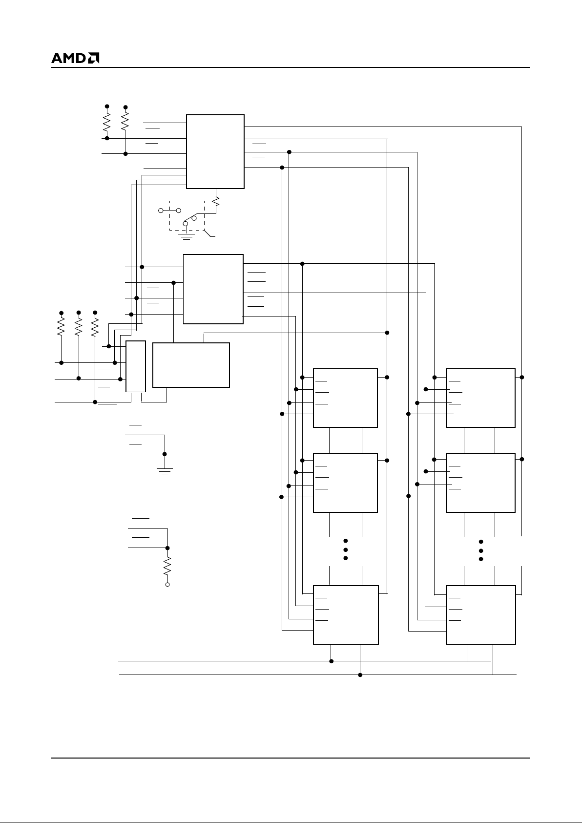
BLOCK DIAGRAM
Notes:
R = 20 K(min)/140 K
Ω
(max)
*1 Mbyte card = S0 + S1, *2 Mbyte card = S0…S3, *4 Mbyte card = S0…S7, *10 Mbyte card = S0…S19
Address
Buffers
and
Decoders
I/O
Transceivers
and
Buffers WP
(Note 1)
A0–A8 D0–D7
Attribute Memory
CE
Write Protect
Switch
V
CC
A0–A18
CEH
0–
CEH
9
CEL
0–
CEL
9
D0–D15
WE
OE
WP
D8–D15
D0–D7
WE
OE
A0
A1–A23*
CE
2
CE
1
A1–A9
A0
CE
2
CE1
REG
CD1
CD
2
Card Detect
BVD1
BVD
2
V
CC
Battery Voltage
Detect
GND
V
CC
10K
V
CC
RR
R
Decoder
V
CC
RR
Am29F040
A0–A18 D0–D7
CE
WE
OE
VSS V
CC
S0*
Am29F040
A0–A18 D8–D15
CE
WE
OE
VSS V
CC
S1*
A0–A18 D0–D7
CE
WE
OE
VSS V
CC
S2*
A0–A18 D8–D15
CE
WE
OE
VSS V
CC
S3*
A0–A18 D0–D7
CE
WE
OE
VSS V
CC
S18*
A0–A18 D8–D15
CE
WE
OE
VSS V
CC
S19*
18723C-1
Page 3
5/4/98 AmC0XXCFLKA 3
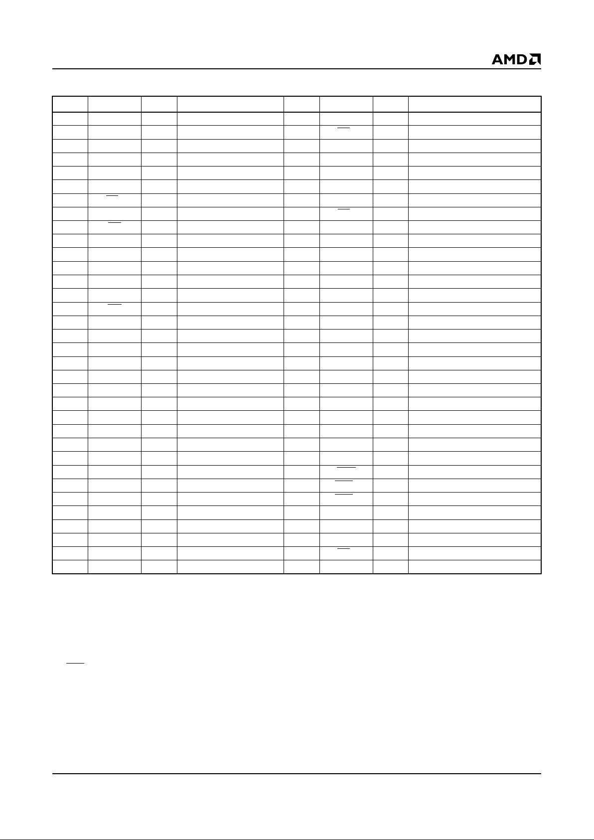
PC CARD PIN ASSIGNMENTS
Notes:
I = Input to card, O = Output from card
I/O = Bidirectional
NC = No connect
In systems which switch V
CC
individually to cards, no signal should be directly connected between cards other than ground.
1. V
PP
not required for Programming or R eading operations.
2. BVD
= Internally pulled-up.
3. Signal must not be connected between cards.
4. Highest address bit for 1 Mbyte card.
5. Highest address bit for 2 Mbyte card.
6. Highest address bit for 4 Mbyte card.
7. Highest address bit for 10 Mbyte card.
Pin# 3 3 Function Pin# Signal I/O Function
1 GND Ground 35 GND Ground
2 D3 I/O Data Bit 3 36 CD1 O Card Detect 1 (Note 3)
3 D4 I/O Data Bit 4 37 D11 I/O Data Bit 11
4 D5 I/O Data Bit 5 38 D12 I/O Data Bit 12
5 D6 I/O Data Bit 6 39 D13 I/O Data Bit 13
6 D7 I/O Data Bit 7 40 D14 I/O Data Bit 14
7CE
1 I Card Enable 1 (Note 3) 41 D15 I/O Data Bit 15
8 A10 I Address Bit 10 42 CE2 I Card Enable 2 (Note 3)
9OE
I Output Enable 43 NC No Connect
10 A11 I Address Bit 11 44 NC No Connect
11 A9 I Address Bit 9 45 NC No Connect
12 A8 I Address Bit 8 46 A17 I Address Bit 17
13 A13 I Address Bit 13 47 A18 I Address Bit 18
14 A14 I Address Bit 14 48 A19 I Address Bit 19 (Note 4)
15 WE
I Write Enable 49 A20 I Address Bit 20 (Note 5)
16 NC No Connect 50 A21 I Address Bit 21 (Note 6)
17 V
CC1
Pow er Supp ly 51 V
CC2
Power Supply
18 NC No Connect (Note 1) 52 NC No Connect (Note 1)
19 A16 I Address Bit 16 53 A22 I Address Bit 22
20 A15 I Address Bit 15 54 A23 I Address Bit 23 (Note 7)
21 A12 I Address Bit 12 55 NC No Connect
22 A7 I Address Bit 7 56 NC No Connect
23 A6 I Address Bit 6 57 NC No Connect
24 A5 I Address Bit 5 58 NC No Connect
25 A4 I Address Bit 4 59 NC No Connect
26 A3 I Address Bit 3 60 NC No Connect
27 A2 I Address Bit 2 61 REG
I Register Select
28 A1 I Address Bit 1 62 BVD2 O Battery V oltage Dete ct 2 (Note 2)
29 A0 I Address Bit 0 63 BVD1 O Battery V oltage Dete ct 1 (Note 2)
30 D0 I/O Data Bit 0 64 D8 I/O Data Bit 8
31 D1 I/O Data Bit 1 65 D9 I/O Data Bit 9
32 D2 I/O Data Bit 2 66 D10 I/O Data Bit 10
33 WP O Write Protect (Note 3) 67 CD
2 O Card Detect 2 (Note 3)
34 GND Ground 68 GND Ground
Page 4
4 AmC0XXCFLKA 5/4/98
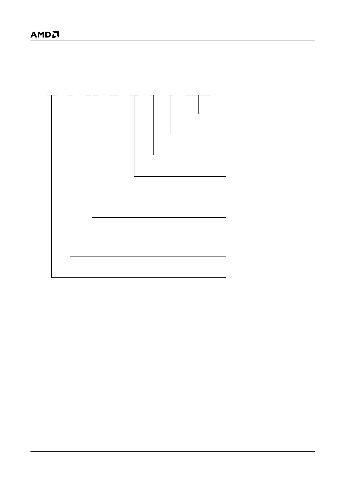
ORDERING INFORMATION
Standard Products
AMD standard produ cts are a vailab le in s ev eral pa ckages a nd operati ng ranges . The orde r number (Valid Combination) is f ormed
by a combination of:
SPEED OPTION
-150 ns
OUTPUT CONFIGURATION:
(x16/x8)
FLASH TECHNOLOGY
PC MEMORY CARD
MEMORY CARD DENSITY
001 = One Megabyte
002 = Two Megabyte
004 = Four Megabyte
010 = Ten Megabyte
AMD
REVISION LEVEL
SERIES
AM C 0XX C FL
K
Axxx
Page 5

5/4/98 AmC0XXCFLKA 5
PIN DESCRIPTION
A0–A23
Address Inputs
These inputs are internally latched during write cycles.
BVD1, BVD2
Battery Voltage Detect
Internally pulled-up.
CD1, CD2
Card Detect
When card detect 1 and 2 = ground the system detects
the card.
CE1, CE2
Card Enable
This input is active low. The memory card is deselected
and power consumption is reduced to standby levels
when CE
is high. CE activates the internal memory
card circuitry that controls the high and low byte control
logic of the card, input buffers segment decoders, and
associated memory devices.
D0–D15
Data Input/Output
Data inputs are internally latched on write cycles. Data
outputs during re ad cycles. Data pins are active high.
When the memory ca rd is deselected or the outputs
are disabled the outputs float to tristate.
GND
Ground
NC
No Connect
Corresponding pin is not co nnec ted i nternally t o th e die .
OE
Output Enable
This input is active low and enables the data buffers
through the card outputs during read cycles.
REG
Attribute Memory Select
This input is active low and enables reading the CIS
from the EEPROM.
V
CC
PC Card Power Supply
For device operation (5.0 V ± 5%).
WE
Write Enable
This input is active low and controls the write function
of the comma nd register to the m emory array. The
target address is latched on the falling edge of the WE
pulse and the appropri ate data is latch ed on the r isin g
edge of the pulse.
WP
Write Protect
This output is active high and disables a ll card write
operations.
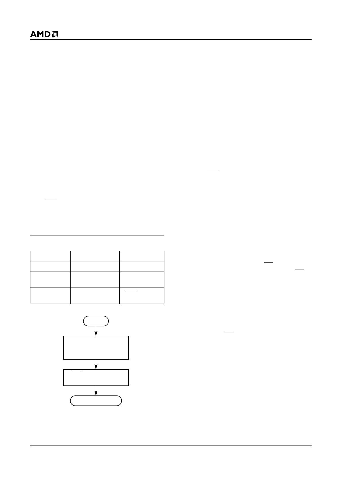
MEMORY CARD OPERATIONS
The “C” series Flash Me mor y Ca rd is org anized as an
array of individual devices. Each device is 512K bytes
in size with eight 64K byte sectors. Although the address space is continuous each physical device defines
a logical address segment size.
Byte-wide erase operations could be performed in
four ways:
■ In increments of the segment size
■ In increments of the sectors in individual segments
■ All eight sectors in parallel within individual
segments
■ Selected sectors of the eight sectors in parallel
within individual segments
Multiple segments may be erased concurrently when
additional I
CC
current is supplied to the device. Once a
memory se ctor or mem or y segm ent i s erased any address location may be programmed. Fla sh technology
allows any logical “1” data bit to be programmed to a
logical “0”. The on ly way to reset bits to a l ogica l “1” is
to erase the entire memory sector of 64K bytes or
memory segment of 512K bytes.
Erase operations are the on ly operations tha t work o n
entire memor y se ctors or memo r y seg men ts. All other
operations such as word-wide programming are not affected by the physical memory segments.
The common memory space data contents are altered
in a similar manner as writing to individual Flash memory devices. On-card address and data buffers activate
the appropriate Flash device in the memory array. Each
device internally latches address and data during write
cycles. Refer to Table 1.
Attribute memor y i s a se parat ely ac c esse d c ar d m emory space. The regis ter memor y space is ac tive when
the REG
pin is driven low. The Card Information Structure (CIS) desc ribes the capa bilities and sp ecification
of a card. The CIS is stored in the attribute memory
space beginning at ad dress 00000H. The “C” ser ies
cards contain a separate 512 byte EEPROM memor y
for the Card Information Structure. D0–D7 are active
during attribute memory accesses. D8–D15 s hould b e
ignored. Odd order bytes present invalid data. Refer to
Table 2.
Page 6
6 AmC0XXCFLKA 5/4/98
Word-Wide Operations
The “C” series cards provide the flexibility to operate on
data in a byte-wide or word-wide format. In word-wide
operations the Low-bytes are controlled with CE
1 when
A0 = 0. The High-bytes are controlled with CE
2 with
A0 = don’t care.
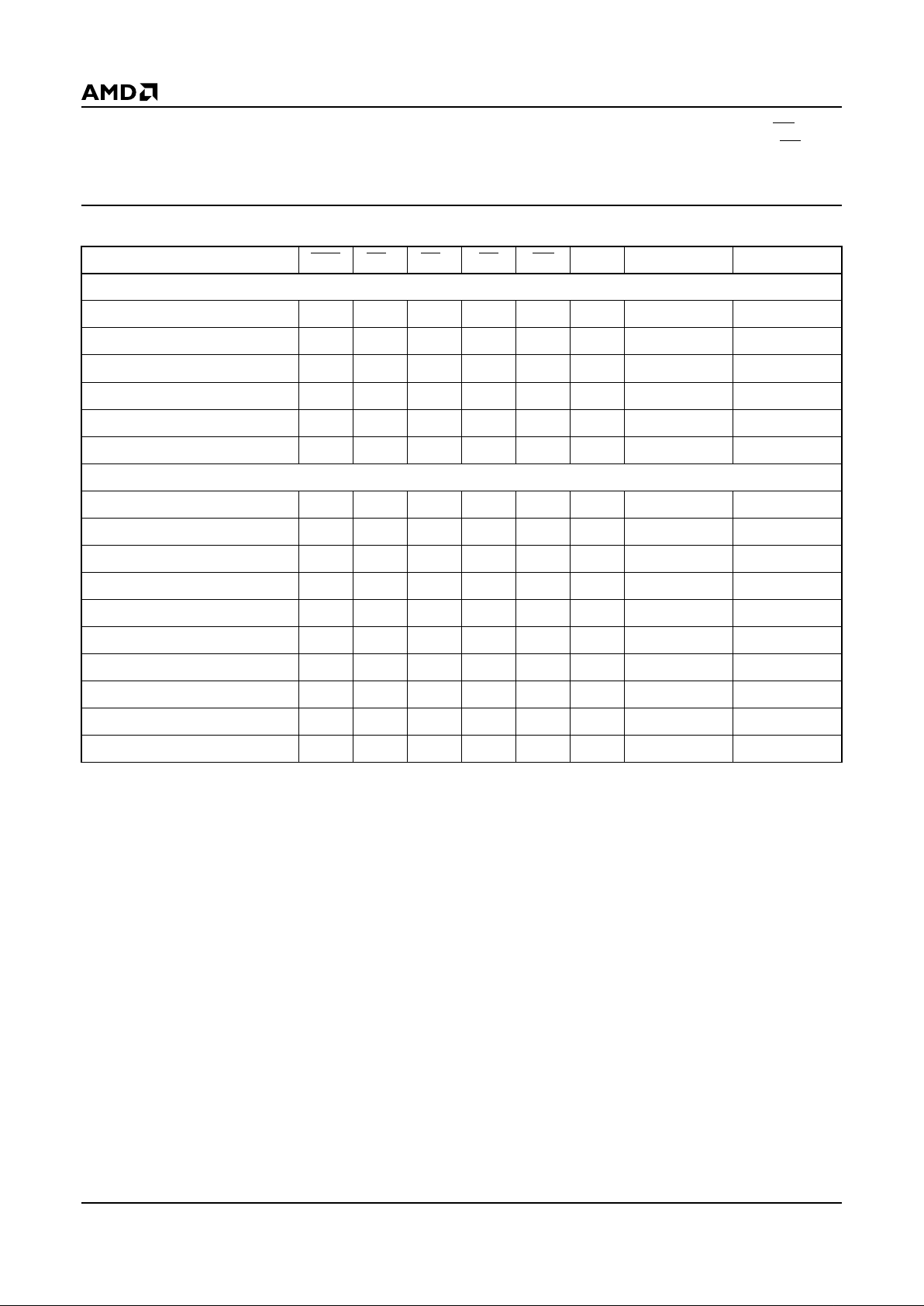
Table 1. Common Memory Bus Operations
Legend:
X = Don’t Care, whe re Don’t Care is either at V
IL
or VIH level. See DC Characteristics for voltage levels of normal TTL or CMOS
input levels.
Notes:
1. V
PP
pins are not connected in th e 5.0 V-Only Flash Memory Card.
2. Manufacturer an d de vice codes ma y be accessed via a com mand registe r write seq uence . (Ref er to A utosel ect Comma nd in
Tables 3 and 4.)
3. Standby current is I
CCS
.
4. Refer to Tables 3 and 4 for valid D
IN
during a byte write operation.
5. Refer to Table 5 for valid D
IN
during a word write operation.
6. Byte access—Even. In this x8 mode, A0 = V
IL
outputs or inputs the “even” byte (low byte) of the x16 word on D0–D7.
7. Byte access—Odd. In this x8 mode, A0 = V
IH
outputs or inputs the “odd” byte (high byte) of the x16 word on D0–D7. This is
accomplished internal to the card by transposing D8–D15 to D0–D7.
8. Odd byte only access. In this x8 mode, A0 = X outputs or inputs the “odd” byte (high byte) of the x16 word on D8–D15.
9. x16 word accesses present both “even” (low) and “odd” (high) bytes. A0 = X.
Pins/Operation REG CE2CE1OEWE A0 D8–D15 D0–D7
READ-ONLY
Read (x8) (Note 6) V
IH
V
IH
V
IL
V
IL
V
IH
V
IL
High-Z Data Out-Even
Read (x8) (Note 7) V
IH
V
IH
V
IL
V
IL
V
IH
V
IH
High-Z Data Out-Odd
Read (x8) (Note 8) V
IH
V
IL
V
IH
V
IL
V
IH
X Data Out-Odd High-Z
Read (x16) (Note 9) V
IH
V
IL
V
IL
V
IL
V
IH
X Data Out-Odd Data Out-Even
Output Disable V
IH
XXVIHV
IH
X High-Z High-Z
Standby (Note 3) X V
IH
V
IH
X X X High-Z High-Z
READ/WRITE
Read (x8) (Notes 2, 6) V
IH
V
IH
V
IL
V
IL
V
IH
V
IL
High-Z Data Out-Even
Read (x8) (Notes 2, 7) V
IH
V
IH
V
IL
V
IL
V
IH
V
IH
High-Z Data Out-Odd
Read (x8) (Notes 2, 8) V
IH
V
IL
V
IH
V
IL
V
IH
X Data Out-Odd High-Z
Read (x16) (Notes 2, 9) V
IH
V
IL
V
IL
V
IL
V
IH
X Data Out-Odd Data Out-Even
Write (x8) (Notes 4, 6) V
IH
V
IH
V
IL
V
IH
V
IL
V
IL
High-Z Data In-Even
Write (x8) (Notes 4, 7) V
IH
V
IH
V
IL
V
IH
V
IL
V
IH
High-Z Data In-Odd
Write (x8) (Notes 4, 8) V
IH
V
IL
V
IH
V
IH
V
IL
X Data In-Odd High-Z
Write (x16) (Notes 5, 9) V
IH
V
IL
V
IL
V
IH
V
IL
X Data In-Odd Data In-Even
Output Disable V
IH
XXVIHV
IL
X High-Z High-Z
Standby (Note 3) X V
IH
V
IH
X X X High-Z High-Z
Volt-only?
Page 7
5/4/98 AmC0XXCFLKA 7
Table 2. Attribute Memory Bus Operations
Legend:
X = Don’t Care, where Don’t Care is either V
IL
or VIH levels. See DC Characteristics for voltage levels of normal TTL or CMOS
input levels.
Notes:
1. V
PP
pins are not connected in th e 5.0 V-Only Flash Memory Card.
2. In this x8 mode, A0 = V
IL
outputs or inputs the “even” byte (low byte) of the x16 word on D0–D7.
3. Only even-byte dat a is valid during Attribute Memory Read function.
4. During Attribute Memory Read function, REG
and OE must be active for the entire cycle.
5. During Attr ibute Memory Write function, REG
and WE must be activ e for the entire cycle, OE must be inactive for the entire
cycle.
6. Standby current is I
CCS
.
Pins/Operation REG CE2CE1OEWE A0 D8–D15 D0–D7
READ-ONLY
Read (x8) (Notes 2, 4) V
IL
V
IH
V
IL
V
IL
V
IH
V
IL
High-Z Data Out-Even
Read (x8) (Notes 3, 4) V
IL
V
IH
V
IL
V
IL
V
IH
V
IH
High-Z Not Valid
Read (x8) (Note 3) V
IL
V
IL
V
IH
V
IL
V
IH
X Not Valid High-Z
Read (x16) (Notes 3, 4, 5) V
IL
V
IL
V
IL
V
IL
V
IH
X Not Valid Data Out-Even
Output Disable V
IL
XXVIHV
IH
X High-Z High-Z
Standby (Note 6) X V
IH
V
IH
X X X High-Z High-Z
READ/WRITE
Read (x8) (Notes 2, 4) V
IL
V
IH
V
IL
V
IL
V
IH
V
IL
High-Z Data Out-Even
Read (x8) (Notes 3, 4) V
IL
V
IH
V
IL
V
IL
V
IH
V
IH
High-Z Not Valid
Read (x8) (Note 4) V
IL
V
IL
V
IH
V
IL
V
IH
X Not Valid High-Z
Read (x16) (Note 4) V
IL
V
IL
V
IL
V
IL
V
IH
X Not Valid Data Out-Even
Write (x8) (Notes 2, 5) V
IL
V
IH
V
IL
V
IH
V
IL
V
IL
High-Z Data In-Even
Write (x8) (Note 5) V
IL
V
IH
V
IL
V
IH
V
IL
V
IH
High-Z High-Z
Write (x8) (Notes 4, 5) V
IL
V
IL
V
IH
V
IH
V
IL
X High-Z High-Z
Write (x16) (Note 5) V
IL
V
IL
V
IL
V
IH
V
IL
X High-Z Data In-Even
Output Disable V
IL
XXVIHV
IL
X High-Z High-Z
Standby (Note 6) X V
IH
V
IH
X X X High-Z High-Z
Volt-only?
Page 8

8 AmC0XXCFLKA 5/4/98
Byte-Wide Operations
Byte-wide data is available on D0–D7 for read and write
operations (CE
1 = low, CE2 = high). Even and odd
bytes are stored in separate memory segments (i.e.,
S0 and S1) and are accessed when A0 is low and high
respectively. The even byte is the low order byte and
the odd byte is the high order byte of a 16-bit word.
Erase operations in the byte-wide mode must ac count
for da ta multip lexin g on D0–D7 by chan ging the s tate of
A0. Each memory sector or memory segment pair
must be addressed separately for erase operations.
Card Detection
Each CD (output) pin s hould be r ead by the host system to determine i f the memory card is adeq uately
seated in the socket. CD
1 and CD2 are internally tied
to ground. If both bits are not detected, the system
should indicate that the card must be reinserted.
Write Protection
The AMD Flash memor y card has thr ee types of writ e
protection. The PCMCIA /JEIDA socket itself provides
the first type of write protection. Power supply and control pins have specific pin lengths in order to protect the
card with proper power supp ly se quenci ng in th e case
of hot insertion and removal.
A mechanical write protect switch provides a second
type of write protectio n. When this switch is act ivated,
WE
is internall y forced high. The Flash mem ory command register is disabled from acce pting any write
commands.
The third type of write protection is achieved with V
CC1
and V
CC2
below V
LKO
. Each Flash memory device that
comprises a Flash memory segment will reset the command register to the read-only mode when V
CC
is
below V
LKO
. V
LKO
is the voltage below which writ e op-
erations to individual command registers are disabled.
MEMORY CARD BUS OPERATIONS
Read Enable
Two Card En able (CE) pin s are available on the memory card. Both CE
pins must be active low for
word-wide read acces ses. O nly on e CE
is required for
byte-wide accesses. The CE
pins control the sel ectio n
and gates power to t he high and low memo ry segments. The Output Enable (OE
) controls gating ac-
cessed data from the memory segment outputs.
The device will automatically power-up in the read/
reset state. In this case, a command s equence is not
required to read data. Standard microprocessor read
cycles will retrieve array data. This default value ensures that no spurious alteration of the memory content
occurs during the power transition. Refer to the AC
Read Characteristics and Waveforms for the specific
timing parameters.
Output Disable
Data outputs from the card are disabled when OE is at
a logic-high level. Under this condit ion, outputs are i n
the high-impedance state.
Standby Operations
Byte-wide read accesse s only r equir e half of the read /
write output buffer (x16) to be active. In addition, only
one memory segment is active within either the high
order or low orde r bank. Activation o f the appropr iate
half of the output buffer is controlled by the combination
of both CE
pins. The CE pins also control power to the
high and low-order banks of memor y. Outputs of the
memory b ank not select ed are placed i n the high impedance state. The individual memory segment is activated by the address decoders. The othe r memory
segments operate in standby. An active memory segment continues to draw power until completion of a
write or erase operation if the card is deselected in the
process of one of these operations.
Auto Select Operation
A host system or external card reader/writer can determine the on-card manufacturer and device I.D. codes.
Codes are available after writing the 90H co mmand t o
the command register of a memory segment per
T ab les 3 and 4. Reading from address location 00000H
in any segment provides the manufacturer I.D. while
address location 00002H provides the device I.D.
To terminate the Auto Select o peratio n, i t is ne ces s ary
to write the Read/Reset command sequence into the
register.
Write Operations
Write and erase operations are valid on ly when V
CC1
and V
CC2
are above 4.75 V. This activates the state
machine of an addressed memory segment. The command register is a latch which saves address, commands, and data information used by the state
machine and memory array.
When Write Enable (WE
) and appropriate CE(s) are at
a logic-level low, and Output Enable (OE
) is at a
logic-high, the command register is enabled for write
operations. The falling edge of WE
latches address information and the rising edge latches data/command
information.
Write or erase operations are performed by writing appropriate data patterns to the command register of accessed Flash memory sectors or memory segments.
The byte-wide and word-wide commands are defined
in Tables 3, 4, and 5, respectively.
Page 9
5/4/98 AmC0XXCFLKA 9
Table 3. Even Byte Command Definitions (Note 5)
* Address fo r Memory Segment 0 (S0) o nly. Address for the higher ev en memo ry segments (S2–S18) = (Addr) + (N/2)* 100 000H
where N = Memory Segment number (0) for 1 Mb yte, N = (0, 2) fo r 2 Mbyte, N = (0, 2, 4, 6) f or 4 Mbyte, N = (0…18) f or 10 Mb yte.
Notes:
1. Address bit A16 = X = Don’t Car e for all ad dress commands e xcept f or Progra m Address (PA), Read Address (RA) and Sector
Address (SA).
2. Bus operations are defined in Table 1.
3. RA = Address of the memory location to be read.
PA = Address of the memory location to be programmed. Addresses are latched on the falling edge of the WE
pulse.
SA = Address of the sector to be erased. The combination of A17, A18, A19 will uniquely select any sector of a segment.
To select the memory segment:1 and 2 Mbyte: Use CE1 and A20
4 Mbyte: Use CE
1 and A20, A21
10 Mbyte: Use CE
1 and A20–A23.
4. RD = Data read from location RA during read operation.
PD = Data to be programmed at location PA. Data is latched on the rising edge of WE pulse .
5. A0 = 0 a nd CE
1 = 0
Embedded
Command
Sequence
Bus
Write
Cycles
Req’ d
First Bus
Write Cycle
Second Bus
Write Cycle
Third Bus
Write Cycle
Fourth Bus
Read/Write Cycle
Fifth Bus
Write Cycle
Sixth Bus
Write Cycle
Addr* Data Addr* Data Addr* Data Addr* Data Addr* Data Addr* Data
Reset/Read 4 AAAAH AAH 5554H 55H AAAAH F0H RA RD
Autoselect 4 AAAAH AAH 5554H 55H AAAAH 90H 00H/02H 01H/A4H
Byte Write 4 AAAAH AAH 5554H 55H AAAAH A0H PA PD
Segment Erase 6 AAAAH AAH 5554H 55H AAAAH 80H AAAAH AAH 5554H 55H AAAAH 10H
Sector Erase 6 AAAAH AAH 5554H 55H AAAAH 80H AAAAH AAH 5554H 55H SA 30H
Sector Erase Suspend Erase can be suspended during sector erase with Addr (don’t care), Data (B0H)
Sector Erase Resume Erase can be resumed after suspend with Addr (don’t care), Data (30H)
Page 10
10 AmC0XXCFLKA 5/4/98
Table 4. Odd Byte Command Definitions (Note 5)
*Address for Memory Segment 1 (S1) only. Address for the higher odd memory segments (S3–S19) = (Addr) + ((N–1)/2)*
100000H + 80000H where N = Memory Segment number (1) for 1 Mbyte, N = (1, 3) for 2 Mbyte, N = (1, 3, 5, 7) for 4 Mbyte,
N = (1…19) for 10 Mbyte.
Notes:
1. Address bit A16 = X = Don’t Car e for all ad dress commands e xcept f or Progra m Address (PA), Read Address (RA) and Sector
Address (SA).
2. Bus operations are defined in Table 1.
3. RA = Address of the memory location to be read.
PA = Address of the memory location to be programmed. Addresses are latched on the falling edge of the WE
pulse.
SA = Address of the sector to be erased. The combination of A17, A18, A19 will uniquely select any sector of a segment.
To select the memory segment:1 and 2 Mbyte: Use CE2 and A20
4 Mbyte: Use CE
2 and A20, A21
10 Mbyte: Use CE
2 and A20–A23.
4. RD = Data read from location RA during read operation.
PD = Data to be programmed at location PA. Data is latched on the rising edge of WE
pulse.
5. A0 = 1 a nd CE
1 = 0 or A0 = X and CE2 = 0.
Embedded
Command
Sequence
Bus
Write
Cycles
Req’d
First Bus
Write Cycle
Second Bus
Write Cycle
Third Bus
Write Cycle
Fourth Bus
Read/Write Cycle
Fifth Bus
Write Cycle
Sixth Bus
Write Cycle
Addr* Data Addr* Data Addr* Data Addr* Data Addr* Data Addr* Data
Reset/Read 4 AAABH AAH 5555H 55H AAABH F0H RA RD
Autoselect 4 AAABH AAH 5555H 55H AAABH 90H 00H/02H 01H/A4H
Byte Write 4 AAABH AAH 5555H 55H AAABH A0H PA PD
Segment Erase 6 AAABH AAH 5555H 55H AAABH 80H AAABH AAH 5555H 55H AAABH 10H
Sector Erase 6 AAABH AAH 5555H 55H AAABH 80H AAABH AAH 5555H 55H SA 30H
Sector Erase Suspend Erase can be suspended during sector erase with Addr (don’t care), Data (B0H)
Sector Erase Resume Erase can be resumed after suspend with Addr (don’t care), Data (30H)
Page 11
5/4/98 AmC0XXCFLKA 11
Table 5. Word Command Definitions (Note 7)
Notes:
1. Address bit A16 = X = Don’t Care for all address commands except for Program Address (PA) and Sector Address (SA).
2. Bus operations are defined in Table 1.
3. RA = Address of the memory location to be read.
PA = Address of the memory location to be programmed. Addresses are latched on the falling edge of the WE
pulse.
SA = Address of the sector to be erased. The combination of A17, A18, A19 will uniquely select any sector of a segment.
To select the memory segment:1 and 2 Mbyte: Use CE
1, CE2, A20
4 Mbyte: Use CE
1, CE2, A20, A21
0 Mbyte: Use CE
1, CE2, A20–A23.
4. RW = Data read from locat ion RA during read operation. (Word Mode).
PW = Data to be programmed at location PA. Data is latched on the rising edge of WE
. (Word Mode).
5. Address for Memory Segment Pair 0 (S0 and S1) only. Address for the higher Memory Segment Pairs (S2, S3 = Pair 1, S4,
S5 = Pair 2, S6, S7 = Pair 3…) is equal to (Addr) + M* (80000H) where M = Memory Segment Pair number.
6. Word = 2 bytes = odd byte and even byte.
7. CE1 = 0 and CE2 = 0.
Table 6. Memory Sector Address Table
for Memory Segment S0
FLASH MEMORY WRITE/ERASE
OPERATIONS
Details of AMD’s Embedded Write and
Erase Operations
Embedded Erase™ Algorithm
The automatic me mory sector or memory segmen t
erase does not require the device to be entirely preprogramming prior to executing the Embedded Erase
command. Upon executing the Embedded Erase command sequence, the addressed memory sector or
memory segment will automatically write and verify the
entire memory segment or memory sector for an all
“zero” data pattern. The system is not requ ired to provide any controls or timing during these operations.
When the memory sector or memory segment is automatically verified to contain an all “zero” pattern, a
self-timed chip erase-and-verify begins. The erase and
verify operations are complete when the data on D7 of
the memory sector or memory segment is “1” (see
“Write Operation Sta tus” section) at which time the
Embedded
Command
Sequence
Bus
Write
Cycles
Req’d
First Bus
Write Cycle
Second Bus
Write Cycle
Third Bus
Write Cycle
Fourth Bus
Read/Write Cycle
Fifth Bus
Write Cycle
Sixth Bus
Write Cycle
Addr* Data Addr* Data Addr* Data Addr* Data Addr* Data Addr* Data
Reset/Read 4 AAAAH AAAA 5554H 5555 AAAAH F0F0 RA RW
Autoselect 4 AAAAH AAAA 5554H 5555 AAAAH 9090 00H/02H
0101/
A4A4
Byte Write 4 AAAAH AAAA 5554H 5555 AAAAH A0A0 PA PW
Segment Erase 6 AAAAH AAAA 5554H 5555 AAAAH 8080 AAAAH AAAA 5554H 5555 AAAAH 1010
Sector Erase 6 AAAAH AAAA 5554H 5555 AAAAH 8080 AAAAH AAAA 5554H 5555 SA 3030
Sector Erase Suspend Erase can be suspended during sector erase with Addr (don’t care), Data (B0H)
Sector Erase Resume Erase can be resumed after suspend with Addr (don’t care), Data (30H)
Sector A19 A18 A17 Address Range
0 0 0 0 00000h-0FFFFh
1 0 0 1 10000h-1FFFFh
2 0 1 0 20000h-2FFFFh
3 0 1 1 30000h-3FFFFh
4 1 0 0 40000h-4FFFFh
5 1 0 1 50000h-5FFFFh
6 1 1 0 60000h-6FFFFh
7 1 1 1 70000h-7FFFFh
Note: A0 is not mapped internally.
Page 12
12 AmC0XXCFLKA 5/4/98
device returns to the Read mode (D15 on the odd
byte). The system is not required to provide any control
or timing during these operations. A Reset command
after the device has begun execution will stop the device but the data in the operated segment will be undefined. In that case, restart the erase on that sector and
allow it to complete.
When using the Embedded Erase algorithm, the erase
automatically terminates when adequ ate erase margin
has been achieved for the memory array (no erase verify command i s requir ed). The m argin voltag es are internally ge nerated in the same man ner as when the
standard erase verify command is used.
The Embedded Erase command sequence is a command only operation that stages the memory sector or
memory segment for automatic electrical erasure of all
bytes in the array. Th e automatic erase beg ins on the
rising edge of the WE
and terminates when the data on
D7 of the memory sector or memory segment is “1”
(see “Write Operation Stat us” section) at which time
the device returns to the Read mode. Plea se note tha t
for the memory segment or memory sector erase operation, Data
Polling may be performed at any address in
that segment or sector.
Figure 1 and Table 7 illustrate the Embedded Erase Al-
gorithm, a typical co mm an d strin g an d b u s op er a ti on s .
As described ear lier, once the memor y sector in a device or memory se gment completes the Embedded
Erase operation it returns to the Read mode and addresses are no longer latched. Therefore, the device
requires that a valid address input to the device is supplied by the system at this particular instant of time.
Otherwise, the system will never read a “1” on D7. A
system designer has two choices to implement the Embedded Erase algorithm:
1. The system (CPU) keeps the sector address (within
any of the sectors being erased) valid during the entire Embedded Erase operation, or
2. Once the system executes the Embedded Erase
command sequence, the CPU takes away the address from the device and becomes free to do other
tasks. In this case, the CPU is required to keep track
of the valid sector address by loading it into a temporary register. When the CPU comes back for performing Data
Polling, it should reassert the sam e
address.
Since the Embedded Erase operation takes a significant amount of time (1.5–30 s), option 2 makes more
sense. However, the choice of these two options has
been left to the system designer.
Sector Erase
Sector erase is a six bus cycle operation. There are two
“unlock” write cycles. These are followed by writing the
“set-up” command. Two more “unlock” write cycles are
then followed by the sector erase command. The sector
address (any address locati on within the desired sector) is latched on the falling edge of WE
, while the com-
mand (data) is latched on the rising edge of WE
. A
time-out of 100 µs from the rising edge of the last sector erase command will initiate the sector erase
command(s).
Multiple sectors may be erased concurrently by writing
the six bus cycle operat ions as descr ibed ab ove. This
sequence is followed with wr ites of the sect or erase
command 30H to addresses in other sectors desired to
be concurrently erased. A time-out of 100 µs from the
rising edge of the WE
pulse for the last sector erase
command will initiate the sector erase. If another sector
erase command is written within the 100 µs time-out
window the timer is reset. Any command other than
sector erase within the time-out window will reset the
device to the read mode, ignoring the previous command string (refer to “Wri te Operation Status” sectio n
for Sector Erase Timer operation). Loa ding the sector
erase buffer may be done in any sequence and with
anysector number.
Sector erase does not requi re the user to program the
device prior to erase. The device automatically programs all memory locations in the sector(s) to be
erased prior to electrical erase. When erasing a sector
Table 7. Embedded Erase Algorithm
Bus Operation Command Comments
Standby Wait for VCC ramp
Write
Embedded Erase
command sequence
6 bus cycle
operation
Read
Data
Polling to
verify erasure
18723C-2
Figure 1. Embedded Erase Algorithm
Write Embedded Erase
Command Sequence
(Table 3 and 4)
Data Poll from Device
(Figure 3)
Start
Erasure Complete
Page 13
5/4/98 AmC0XXCFLKA 13
or sectors the remaining unselected sectors are not affected. The system is not required to provide any controls or timings during these operations. A Reset
command after the device has begun execution will
stop the device but the data i n the operated segm ent
will be undefined. In that case, restart the erase on that
sector and allow it to complete.
The automatic sector erase begins after the 100 µs
time out from th e rising ed ge of the WE
pulse for the
last sector erase command pulse and terminates when
the data on D7 is “1” (see “Write Operation Status” section) at which time the d evice returns to read m ode.
Data
Polling must be performed at an address within
any of the sectors being erased.
Figure 1 illustrates th e Embedded Erase Algori thm
using typical command strings and bus operations.
Embedded Program™ Algorithm
The Embedded Program Setup is a four bus cycle o peration that stages the addres sed memory sec tor or
memory segment for automatic programming.
Once the Embedded P rogram Setup operation i s performed, the next WE
pulse causes a transition to an active programming operation. Addresses are internally
latched on the falling edge of the WE
pulse. Data is in-
ternally latched on the rising edge of the WE
pulse. T he
rising edge of WE
also begins the programming operation. The system is not required to provide further control or timing. The device will automati cally provide an
adequate inter nally generated wr ite pulse and verify
margin. The automatic programming operation is completed when the data o n D7 of the a ddres s ed mem ory
sector or memory segment is equivalent to data written
to this bit (see Write Operation Status section) at which
time the device returns to the Read mode (no write verify command is required).
Addresses are latched on the falling edge of WE
during
the Embedded Program command execution and
hence the system is not required to keep the addresses
stable during the entire Programm ing operation. However, once the device completes the Embedded Program operation, it returns to the Read mode and
addresses are no longer latched. Therefore, the device
requires that a valid address input to the device is supplied by the system at this particular i nstant of time.
Otherwise, the system will never read a valid data on
D7. A system designer has two choices to imple ment
the Embedded Programming algorithm:
1. The system (CPU) keeps the address valid dur ing
the entire Embedded Programming operation, or
2. Once the system executes the Embedded Program-
ming command sequence, the CPU takes away the
address from the device and becomes free to do
other tasks. In this case, the CPU is required to
keep track of the valid address by loading i t into a
temporary regis ter. When the CPU comes back for
performing Data
Polling, it should reassert the same
address.
However , since the Embedded Programming operation
takes only 16 µs typically, it may be easier for the CPU
to keep the address stable during the entire Embedded
Programming operation instead of reasserting the valid
address during Data
Poll ing. An yw a y, this has been left
to the system desi gner’s choice to go for eith er operation. Any commands written to the segment during this
period will be ignored.
Figure 2 and Table 8 illustrate the Embedded Program
Algorithm, a typical comm and string, an d bus o perat ion.
Reset Command
The Reset command initiali zes the sector or segment
to the read mode. Please refer to Tables 3 and 4, “Byte
Command Definitions,” and Table 5, “Word Command
Definitions” for the Reset com mand operation. The
sector or segment r emains enabled for reads unti l the
command register contents are altered. There is a 6 µs
Write Recovery Time before Read for the first read
after a write.
The Reset command will safely reset the segment
memory to th e Read mode. Memor y content s are not
altered. Following any other command, write the Reset
command once to the segment. This will safely abor t
any operation and reset the device to the Read mode.
The Reset is needed to terminate the auto select operation. It can b e used to ter minate an E rase or Sect or
Erase operation, but the data in the s ec tor or seg men t
being erased would then be undefined.
Write Operation Status
Data Polling—D7 (D15 on Odd Byte)
The Flash Memory PC Card features Data
Polling as a
method to indicate to the host system that the Embedded algorithms are either in progress or completed.
While the Embedded Programming algori thm is in operation, an attempt to read th e device will prod uce th e
complement of expected valid data on D7 of the addressed memory sector or memor y segment. Upon
Table 8. Embedded Program Algorithm
Bus Operation Command Comments
Standby Wait for VCC ramp
Write
Embedded Progr am
command sequence
3 bus cycle
operation
Write
Program
Address/Data
1 bus cycle
operation
Read
Data
Polling to
verify program
Page 14

14 AmC0XXCFLKA 5/4/98
completion of the Embedded Program algorithm an attempt to read the device will produce valid data on D7.
The Data
Polling feature is valid after the rising edge of
the fourth WE
pulse of the four write pulse sequence.
While the Embedded Erase algorithm is in operation,
D7 will read “0” until the erase operat io n is c om pl eted .
Upon completion of the erase operation, the data on D7
will read “1”.
The Data
Polling feature is only active during the E mbedded Programming or Erase algorithms. Please note
that the AmC0XXCFLKA data pin (D7) may change
asynchronousl y while Output Enable (OE
) is asserted
low. This means that the device is driving status information on D7 at one instant of time and then the byte’s
valid data at the next instant of time. Depending on
when the system samples the D7 output, it may read either the status or valid data. Even if the device has
completed the Embedded operation and D7 has a valid
data, the data outputs on D0–D6 may be still invalid
since the switching time for data bits (D0–D7) will not
be the same. This happens since the internal delay
paths for data bits (D0–D7) within the device are different. The valid data will be provided only afte r a ce rtain
time delay (<t
OE
). Please refer to Figure 4a for detailed
timing diagrams.
See Figures 3 and 5 for the Data
Polling timing
specifications and diagrams.
Toggle Bit—D6 (D14 on Odd Byte)
The Flash Memory PC Card also features a “Toggle Bit”
as a method to indicate to the host system that the Embedded algorithms are either in progress or have been
completed.
While the Embedd ed P r ogram or Erase al gorithm is in
progress, successive attempts to read data from the
device will result in D6 toggling between one and zero.
Once the Embedded Program or Erase algorithm is
completed, D6 will stop toggling and valid data on
D0–D7 will be read on the next successive read attempt. The Toggle bit is also used for entering Erase
Suspend mode. Please refer to the section entitle d
“Sector Erase Suspend.”
Please note that even if the device completes the Embedded algorithm operation and D6 stops toggling ,
data bits D0–D7 (including D6) may not be valid during
the current bus cycle. This may happen since the internal circuitry may be switching fro m statu s mode t o the
Read mode. There is a time delay associated wi th th is
mode switching. Since this time delay is always less
than t
OE
(OE access tim e), the ne xt succ essive read at-
tempt (OE
going low) will provide the valid data on D0D7. Also note that once the D6 bit has stopped toggling
and the output enable OE
is held low thereafter (without toggling) the data bits (D0–D7) will be valid after
t
OE
time delay.
See Figures 4 and 6 for the Data
Polling diagram and
timing specifications.
18723C-3
Figure 2. Embedded Programming Algorithm in Byte-Wide Mode
Write Embedded Write Command
Sequence per Table 3 or 4
Verify Byte
No
Yes
Data Poll Device
Yes
Increment Address
No
Start
Completed
Last
Address
Page 15

5/4/98 AmC0XXCFLKA 15
Sector Erase Suspend
Sector Erase Suspend command allows the user to interrupt the chip and then do data reads (not program)
from a non-busy sector while it is in the middle of a
Sector Erase operation (which may take up to several
seconds). This command is applicable ONLY during
the Sector Erase operation and will be ignored if written
during the chip Erase or P rogramming operation. The
Erase Suspend command (B0H) will be allowed only
during the Secto r Erase O pe ration th at wi ll i nc lude the
sector erase time-out period after the Sector Erase
commands (30H). Writing this command duri ng the
time-out will result in immediate termination of the
time-out period. Any subsequent writes of the Sector
Erase command will be ignored as such, but instead
will be taken as the Erase Resume command. Note
that any other commands during the time out will reset
the device to read mode. The addresses are
don’t-cares in writing the Erase Suspend or Erase
Resume commands.
When the Sector Erase Suspend command is written
during a Sector Erase operat ion, the chip wil l take between 0.1 µs to 10 µs to suspend the erase operatio n
and go into erase suspended read mode (pseudo-read
mode), during which the user can read from a sector
that is NOT being erased. A read from a sector being
erased may result in invalid data. The user must monitor the toggle bit (D6) to deter mine if the chip has entered the pseudo-re ad mode, at which time the to ggle
bit stops toggling. Note that the user must keep track of
what state the chip is in since there is no external indication of whether the chip is in pse udo-read mode or
actual read mode. After the user writes the Sector
Erase Suspend command and waits until the toggle bit
stops toggling, data reads from the device may then be
performed. Any further writes of the Sector Erase Suspend command at this time will be ignored.
Every time a Sector Erase Suspend command followed
by an Erase Resume command is writ ten, the inter nal
(pulse) counters are reset. These counters are used to
count the number of high voltage pulses the memory
cell requires to program o r eras e. If the c ou nt exceeds
a certain limit, then the D5 bit will be set (Exceede d
Time Limit flag). This resetting of the counters is necessary since the Erase Suspend command can potentially interrupt or disrupt the high voltage pulses.
To resume the operation of S ec tor E rase, the Resum e
command (30H) should be written. Any further writes of
the Resume command at this point wi ll be ig nore. Another Sector Erase Sus pend comman d can be w ritte n
after the chip has resumed.
Page 16

16 AmC0XXCFLKA 5/4/98
Write Operation Status
Table 9. Hardware Sequence Flags
Note: D0, D1, and D2 are reserve pins for future use. D4 is for AMD internal use only.
Status D7D6D5D3 D2–D0
In Progress
Auto-Programming D7 Toggle 0 0
Programming in Auto-Erase 0 Toggle 0 1 (D)
Erasing in Auto-Erase 0 Toggle 0 1
Exceeded
Time Limits
Auto-Programming D
7 Toggle 1 0
Programming in Auto-Erase 0 Toggle 1 1 (D)
Erasing in Auto-Erase 0 Toggle 1 1
Start
Fail
No
D7 = Data?
No
Pass
Yes
No
Yes
D7 = Data?
D5 = 1?
Yes
Read Byte
(D0–D7)
Addr = VA
Read Byte
(D0–D7)
Addr = VA
18723C-4
Note: D7 is rechecked even if D5 = 1 because D7 may change simultaneously with D5.
Figure 3. Data Polling Algorithm
VA = Valid Address
VA = Byte addr for Write
operation
VA = Any segment (sector)
address during segment
(sector) erase operation
Page 17

5/4/98 AmC0XXCFLKA 17
Start
Fail
Yes
D6 = Toggle?
Yes
Pass
No
No
Yes
D6 = Toggle?
D5 = 1?
No
Read Byte
(D0–D7)
Addr = VA
Read Byte
(D0–D7)
Addr = VA
18723C-5
Note: D6 is rechecked even if D5 = 1 because D6 may stop toggling at the same time as D5 changes to “1”.
Figure 4. Toggle Bit Algorithm
VA = Valid Address
VA = Byte addr for Write
operation
VA = Any segment (sector)
address during segment
(sector) erase operation
Page 18

18 AmC0XXCFLKA 5/4/98
18723C-6
* D7 = Valid Data (The device has completed the Embedded operation.)
Figure 5. AC Waveforms for Data Polling During Embedded Algorithm Operations
D0–D6
Valid Data
t
OE
D7 =
Valid Data
High-Z
CE
OE
WE
D7
D
7
D0–D6
D0–D6 = Invalid
*
t
OEH
t
CE
t
CH
t
DF
t
OH
t
WHWH 3 or 4
18723C-7
* D6 stops toggling (The device has completed the Embedded operation.)
Figure 6. AC Waveforms for Toggle Bit During Embedded Algorithm Operations
CE
t
OEH
WE
OE
D6 =
Stop Toggling
D0–D7
Valid
D6 = Toggle
D6 = Toggle
Data
(D0–D7)
*
t
OE
Page 19

5/4/98 AmC0XXCFLKA 19
EMBEDDED ALGORITHMS
18723C-8
Figure 7. Byte-Wide Programming and Erasure Overview
Software polling from
memory segment
Write Embedded
Programming or Erase
command sequence to
memory segments
Completed
The Embedded Algorithm opera tions comple tely automate
the programming and erase procedure by internally executing the algorithm ic comma nd sequen ce of origin al AMD
devices. The devices automatically provide Write Operation Status information with standard read operations.
See Table 3 or 4 for Program Command Sequence.
Start
Page 20

20 AmC0XXCFLKA 5/4/98
EMBEDDED ALGORITHMS
18723C-9
Figure 8. Byte-Wide Programming Flow Chart
Activity
Initialize Programming Variables:
EF = Error Flag
PGM =Embedded Byte Write Command
Sequence Cycle #1–3 (Table 3 or 4)
ADRS = Appropriate address for memory segment
PD = Program Data
VDAT = Valid Data
FMD = Flash Memory Data
EF = 0 = No Programming error
EF = 1 = Programming error
Program Complete
Initialization:
EF = 0
Wait 16 µs
Read ADRS/FMD
Program Error
Begin
Programming
Write PGM
Get ADRS/PD
VDAT = PD
Write ADRS/PGM
Write ADRS/VDAT
No
Yes
Yes
Yes
No
FMD = VDAT
No
FMD = VDAT
More Data
Begin softwar e
polling subroutine
(Figure 9)
Page 21

5/4/98 AmC0XXCFLKA 21
EMBEDDED ALGORITHMS
D5 = 1?
18723C-10
Note: D7 is checked even if D5 = 1 because D7 may have changed simultaneously with D5 or immediately after D5.
Figure 9. Byte-Wide Software Polling for Programming Subroutine
V A = Byte Address for Programming
D5 = 1
No = Program time not exceeded limit
Yes = Program time exceed limit, device failed
EF = Error Flag
Start
Subroutine
No
Yes
Yes
Yes
No
D7 = Data?
No
D7 = Data
Subroutine
Return
Recommend 16 µs
time out from previous
data polling
Device failed
to program
EF = 1
Device Passed
Read Byte
(D0–D7)
Addr = VA
Read Byte
(D0–D7)
Addr = VA
Page 22

22 AmC0XXCFLKA 5/4/98
EMBEDDED ALGORITHMS
18723C-11
Figure 10. Byte-Wide Erasure Flow Chart
Activity
EF = Error Flag = 0
SEG ADRS = Segment Address = 0
ERS = Erase Command Sequence
(Even byte per Table 3, Odd byte per Table 4)
3 seconds wait = 2 seconds memory segment
preprogram time +1 second
memory segment erase time
FMD = Flash Memory Data
FFH = Erased Flash Memory Data
Erase Complete
Wait 3 seconds
Erase Error
Begin
Erase
No
Yes
Yes
Yes
No
FMD = FFH
No
FMD = FFH
Last Segmen t
Address
Initialization:
EF = 0
SEG ADRS = 0
Write ERS cycle
#1–5
Write SEGADRS/ERS
cycle #6
Read SEG
ADRS/FMD
Begin softwar e
polling subroutine
(Figure 11)
Increment SEG ADRS
Page 23

5/4/98 AmC0XXCFLKA 23
EMBEDDED ALGORITHMS
D5 = 1?
18723C-12
Figure 11. Byte-Wide Software Polling Erase Subroutine
X = Don’t Care
D7 = 1
Yes = Erase Complete
No = Erase not Complete
D5 = 1
Yes = Erase time exceeded limit, device failed
No = Erase time has not exceeded limit
Start
Subroutine
No
Yes
Yes
Yes
No
D7 = 1?
No
D7 = 1
Subroutine
Return
Device failed
to program
EF = 1
Device Passed
Read Byte
(D0–D7)
Addr = X
Read Byte
(D0–D7)
Addr = X
Page 24

24 AmC0XXCFLKA 5/4/98
WORD-WIDE PROGRAMMING AND
ERASING
Word-Wide Programming
The Word-Wide Programming sequence will be as
usual per Table 5. The Program wo rd command i s
A0A0H. Each byte is i ndependently pro grammed. For
example, if the high byte of the word indicates the successful comple tion o f programmin g via one o f its wr ite
status bits such as D15, software polling should continue to monitor the low byte for write co mpletion and
data verification, or vice versa. During th e Embedded
Programming operations the device executes programming pulses in 16 µs increments. Status reads provide
information on the progress of the byte programming
relative to the last complete write pulse. Status information is automati call y upd ated u pon c omple tion o f e ach
internal write pulse. Status information does not
change within the 16 µs write pulse width.
Word-Wide Eras ing
The Word-Wide Erasing of a memor y segment pair is
similar to word-wide programming. T he erase word
command is a 6 bus cycle command sequence per
Table 5. Each byte is independently erased and verified. Word-wide erasure reduces total erase time when
compared to byte erasure. Each Flash memor y device
in the card may erase at different rates. Therefore each
device (byte) must be verified separately.
18723C-13
Figure 12. Embedded Algorithm Wor d-Wide Programming and Erasure Overview
Software polling from
memory segments
Write Embedded
Programming or Erase
command sequence to
memory segments
Completed
The Embedded Algorithm opera tions comple tely automate
the parallel programming and erase procedures by internally executing the algorithmic command sequences of
AMD’s Flashrite and Flasherase algorithms. The devices
automatically provide Write Operation Status information
with standard read operations.
See Table 5 for Program Command Sequence.
Start
Page 25

5/4/98 AmC0XXCFLKA 25
EMBEDDED ALGORITHMS
18723C-14
Figure 13. Word-Wide Programming Flow Chart
Activity
Initialize Programming Variables:
EF = Error Flag
EF = 0 = No failure
EF = 1 = Low byte program error
EF = 2 = High byte program error
EF = 3 = Word-wide program error
VWDAT = Valid Word Data
PGM =Embedded Word Write Command
Sequence Cycle #1–3 (Table 5)
ADRS = Appropriate address for Memory Segment
(Cycle #4)
PDW = Program Data Word
FMD = Flash Memory Data
Program Complete
Initialization:
EF = 0
Program Error
Begin
Programming
No
Yes
Yes
Yes
No
FMD = VWDAT
No
FMD = VWDAT
More Data
Get ADRS/PDW
VWDAT = PDW
Write PGM
Write ADRS/PDW
Wait 16 µs
Read ADRS/FMD
Begin softwar e
polling subroutine
(Figure 14)
Page 26

26 AmC0XXCFLKA 5/4/98
EMBEDDED ALGORITHMS
18723C-15
Figure 14. Word-Wide Software Polling Program Subroutine
VA = Word Address for Programming
V
data
= Valid data
D5/13 = 1?
Yes = Erase time has exceeded limit, device failed
No = Erase time has not exceeded limit
Start
Subroutine
Yes
No
D7 = V
data
?
Yes
D15 = V
data
?
Subroutine
Return
Low byte program
time exceeded limit,
EF = 1
Read Byte
(D0–D7)
Addr = VA
Read Byte
(D8–D15)
Addr = VA
No
D5 = 1?
Read Byte
(D0–D7)
Addr = VA
Yes
No
D7 = V
data
?
No No
D13 = 1?
Read Byte
(D8–D15)
Addr = VA
No
D15 = V
data
?
Yes
Yes
High byte program
time exceeded limit,
EF = 2 + EF
Yes
Page 27

5/4/98 AmC0XXCFLKA 27
EMBEDDED ALGORITHMS
18723C-16
Figure 15. Word-Wide Erasure Flow Chart
Activity
EF = Error Flag
EF = 0 = No failure
EF = 1 = Low byte erase error
EF = 2 = High byte erase error
EF = 3 = Word-wide erase error
SEG ADRS = Segment Address
ERS = Segment Eras e Comman d Sequence (Table 5)
FMD = Flash Memory Data
Erase Complete
Wait 3 seconds
Erase Error
Begin
Erase
No
Yes
Yes
Yes
No
FMD = FFFFH
No
FMD = FFFFH
Last Segmen t
Address
Read SEG
ADRS/FMD
Begin softwar e
polling subroutine
(Figure 16)
Increment SEG ADRS
Write ERS
cycle #6:
SEG ADRS
Initialization:
EF = 0
SEG ADRS = 0
Write ERS
cycle #1–5
Page 28

28 AmC0XXCFLKA 5/4/98
EMBEDDED ALGORITHMS
18723C-17
Figure 16. Word-Wide Software Polling Erase Subroutine
D7/15 = 1
Yes = Erase complete
No = Erase not complete
D5/13 = 1
Yes = Erase time has exceeded limit, device failed
No = Erase time has not exceeded limit
Start
Subroutine
Yes
No
D7 = 1?
Yes
D15 = 1?
Subroutine
Return
Low byte program
time exceeded limit,
EF = 1
Read Byte
(D0–D7)
Read Byte
(D8–D15)
No
D5 = 1?
Read Byte
(D0–D7)
Yes
No
D7 = 1?
No No
D13 = 1?
No
D15 = 1?
Yes
High byte program
time exceeded limit,
EF = 2 + EF
Yes
Read Byte
(D8–D15)
Yes
Page 29

5/4/98 AmC0XXCFLKA 29
ABSOLUTE MAXIMUM RATINGS
Storage Temperature . . . . . . . . . . . . . –30°C to +70°C
Ambient Temperature
with Power Applied. . . . . . . . . . . . . . . –10°C to +70°C
Voltage at All Pins (Note 1) . . . . . . . .–2.0 V to +7.0 V
V
CC
(Note 1). . . . . . . . . . . . . . . . . . . . .–0.5 V to 6.0 V
Output Short Circuit Current (Note 2) . . . . . . . 40 mA
Notes:
1. Minimum DC voltage on input or I/O pins is –0.5 V . During
voltage transitions, inputs may overshoot VSS to –2.0 V
for periods o f up to 2 0 ns. M aximum DC v oltage on output
and I/O pins is VCC + 0.5 V. Dur ing voltage transitions,
outputs may overshoot to V
CC
+ 2.0 V for periods up to
20 ns.
2. No more than one output shorted at a time. Durations of
the short circuit should not be greater than one second.
Conditions equal V
OUT
= 0.5 V or 5.0 V, VCC = VCC max.
These values are chosen to avoid test problems caused
by tester ground degradation. This parameter is sampled
and not 100% test ed, b ut guar anteed b y c haracteriza tion.
3. V
PP1
and V
PP2
are not conn ected.
Stresses above those listed under “Absolute Maximum
Ratings” ma y cause permanent d amage to the de vice . This is
a stress rating only; functional operatio n of the device at
these or any other condi tions abo ve th ose indica ted in the o perational sections of this specification is not implied. Expo-
sure of the device to absolute maximum rating conditions for
extended periods may affect device reliability.
OPERATING RANGES
Commercial (C) Devices
Case Temperature (T
C
). . . . . . . . . . . . . .0°C to +60°C
V
CC
Supply Voltages. . . . . . . . . . . . +4.75 V to 5.25 V
Operating ranges define those limits between which the
functionality of the device is guaranteed.
Page 30

30 AmC0XXCFLKA 5/4/98
DC CHARACTERISTICS
Byte-Wide Operation
Notes:
1. For TTL input voltage levels (V
IL
or VIH), the minimum limit should be increased by: 1 mA for 1 Mbyte
3 mA for 2 Mbyte
7 mA for 4 Mbyte
19 mA for 10 Mbyte.
2. One Flash device active, all the others in standby.
Parameter
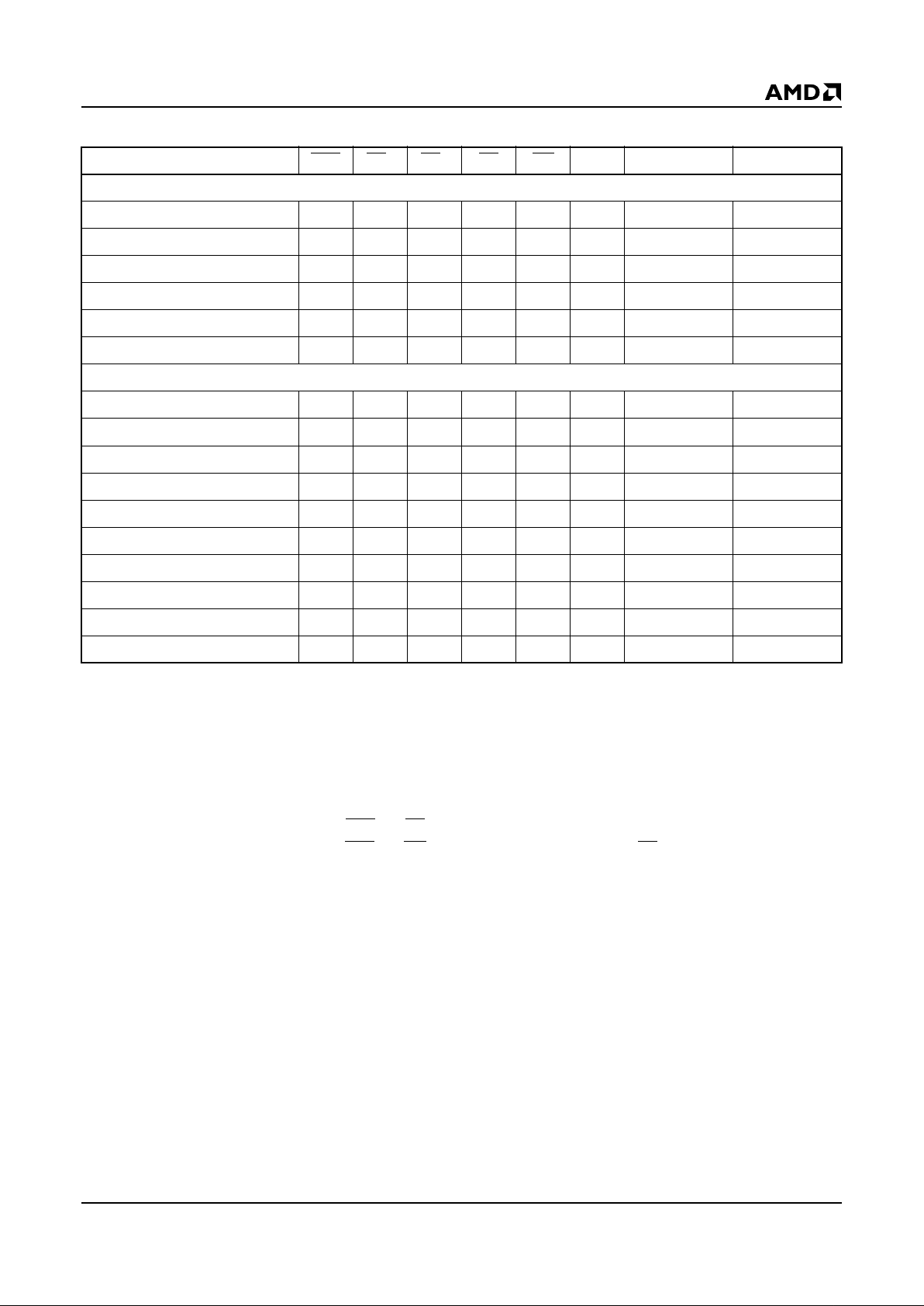
Symbol Parameter Description Test Description Min Max Unit
I
LI
Input Leakage Current
V
CC
= VCC Max, VIN = VCC or V
SS
For all cards:
(CE
, REG, WE, OE = –300 µA Min)
1 MB –300 + 20
µA
2 MB –300 + 20
4 MB –300 + 20
10 MB –300 + 20
I
LO
Output Leakage Current
V
CC
= VCC Max,
V
OUT
= VCC or V
SS
1 MB ± 20
µA
2 MB ± 20
4 MB ± 20
10 MB ± 20
I
CCS
VCC Standby Current (Note 1)
V
CC
= VCC Max
CE
= VCC ± 0.2 V
V
IN
= VCC or GND
1 MB 0.7
mA
2 MB 0.9
4 MB 1.3
10 MB 2.5
I
CC1
VCC Active Read Current
(Notes 1, 2)
VCC = VCC Max, CE = VIL,
OE
= VIH, I
OUT
= 0 mA, at 3.3 MHz
45 mA
I
CC2
VCC Write/Erase Current
(Notes 1, 2)
CE = V
IL
Programming in Progress
65 mA
V
IL
Input Low Voltage –0.5 0.8 V
V
IH
Input High Voltage 2.4 V
CC
+ 0.3 V
V
OL
Output Low Voltage IOL = 3.2 mA, VCC = VCC Min 0.40 V
V
OH
Output High Voltage IOH = 2.0 mA, VCC = VCC Min 3.8 V
CC
V
V
LKO
Low VCC Lock-Out Voltage 3.2 4.2 V
Page 31

5/4/98 AmC0XXCFLKA 31
Word-Wide Operation
Notes:
1. For TTL input voltage levels (V
IL
or VIH), the minimum limit should be increased by: 2 mA for 2 Mbyte
6 mA for 4 Mbyte
18 mA for 10 Mbyte.
2. Two Flash devices active, all the others in standby
Parameter
Symbol Parameter Description Test Description Min Max Unit
I
LI
Input Leakage Current
V
CC
= VCC Max, VIN = VCC or V
SS
(CE, REG, WE, OE = –300 µA Min)
1 MB –300 + 20
µA
2 MB –300 + 20
4 MB –300 + 20
10 MB –300 + 20
I
LO
Output Leakage Current VCC = VCC Max, V
OUT
= VCC or V
SS
1 MB ± 20
µA
2 MB ± 20
4 MB ± 20
10 MB ± 20
I
CCS
VCC Standby Current (Note 1)
V
CC
= VCC Max
CE
= VCC ± 0.2 V
V
IN
= VCC or GND
1 MB 0.7
mA
2 MB 0.9
4 MB 1.3
10 MB 2.5
I
CC1
VCC Active Read Current
(Notes 1, 2)
VCC = VCC Max, CE = VIL,
OE
= VIH, I
OUT
= 0 mA, at 3.3 MHz
90 mA
I
CC2
VCC Programming Current
(Notes 1, 2)
CE = V
IL
Programming in Progress
130 mA
V
IL
Input Low Voltage –0.5 0.8 V
V
IH
Input High Voltage 2.4 V
CC
+ 0.3 V
V
OL
Output Low Voltage IOL = 3.2 mA, VCC = VCC Min 0.40 V
V
OH
Output High Voltage IOH = 2.0 mA, VCC = VCC Min 3.8 V
CC
V
V
LKO
Low VCC Lock-Out Voltage 3.2 4.2 V
Page 32

32 AmC0XXCFLKA 5/4/98
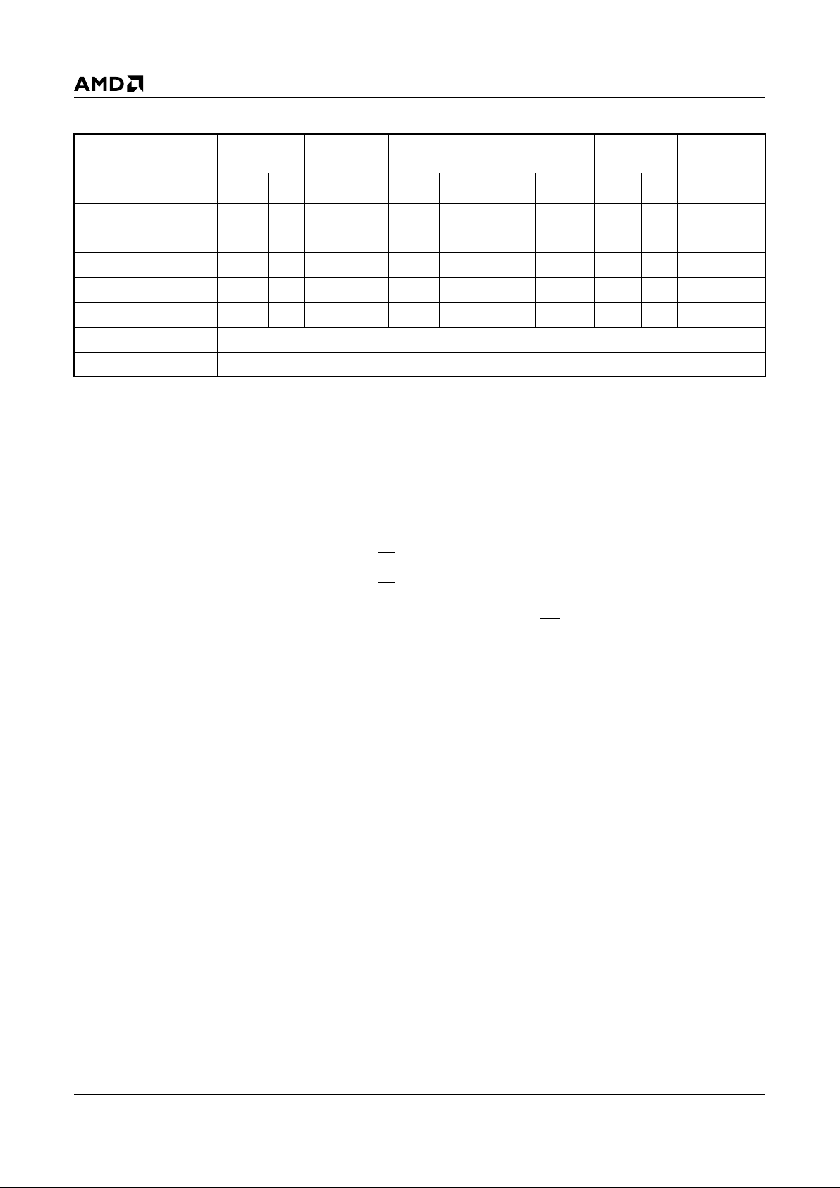
PIN CAPACITANCE
Notes:
1. Sampled, not 100% tested.
2. Test conditions TA = 25°C, f = 1.0 MHz.
SWITCHING AC CHARACTERISTICS
Read Only Operation (Note 1)
Note:
1. Input Rise and Fall Times (10% to 90%): ð 10 ns, Input Pulse levels:
VOL and VOH, Timing Measurement Reference Level: Inputs—VIL and VIH
Outputs—V
IL
and V
IH
Parameter Symbol Parameter Description Test Conditions Max Unit
C
IN1
All except A1–A9 V
IN
= 0 V 31 pF
C
OUT
Output Capacitance V
OUT
= 0 V 31 pF
C
IN2
A1–A9 VIN = 0 V 45 pF
C
I/O
I/O Capacitance D0–D15 V
I/O
= 0 V 31 pF
Card Speed
Parameter Symbol
Parameter Description
-150 ns
UnitJEDEC Standard Min Max
t
AVAV
t
RC
Read Cycle Time 150 ns
t
ELQV
t
CE
Chip Enable Access Time 150 ns
t
AVQV
t
ACC
Address Access Time 150 ns
t
GLQV
t
OE
Output Enable Access Time 75 ns
t
ELQX
t
LZ
Chip Enable to Output in Low-Z 5 ns
t
EHQZ
t
DF
Chip Disable to Output in High-Z 75 ns
t
GLQX
t
OLZ
Output Enable to Output in Low-Z 5 ns
t
GHQZ
t
DF
Output Disable to Output in High-Z 75 ns
t
AXQX
t
OH
Output Hold from First of Address, CE, or OE Change 5 ns
t
WHGL
Write Recovery Time Before Read 6 µs
Page 33

5/4/98 AmC0XXCFLKA 33
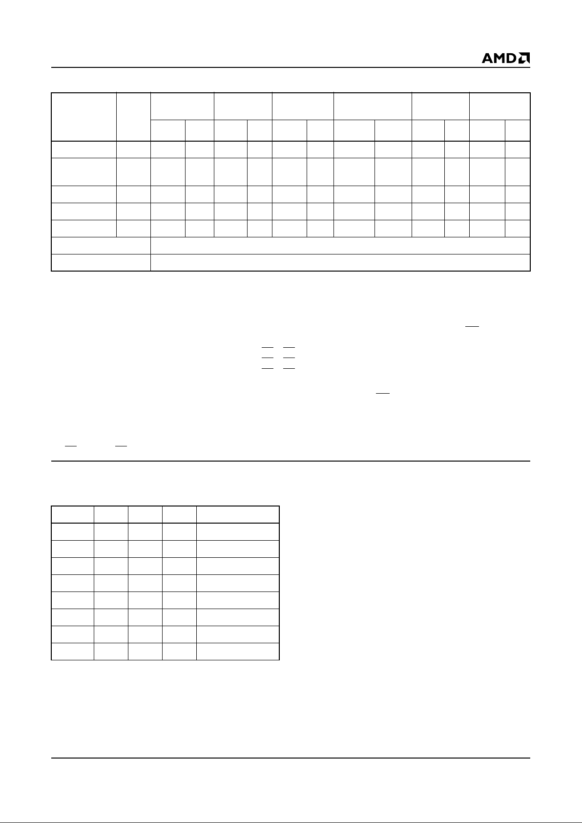
AC CHARACTERISTICS
Write/Erase/Program Operations
Notes:
1. Rise/Fall ð 10 ns.
2. Maximum specific ation not needed due to the devic es internal stop timer that will stop any er ase or write operatio n that exce ed
the device specification.
3. Embedded Program Operation of 16
µ
s consist of 10 µs program pulse and 6 µs write recovery before read. This is the
minimum time for one pass through the programming algorithm. D5 = “1” only after a byte takes longer than 48 ms to Write.
Card Speed
Parameter Symbol
Parameter Description
-150 ns
UnitJEDEC Standard Min Typ Max
t
AVAV
t
WC
Write Cycle Time 150 ns
t
AVWL
t
AS
Address Setup Time 20 ns
t
WLAX
t
AH
Address Hold Time 55 ns
t
DVWH
t
DS
Data Setup Time 50 ns
t
WHDX
t
DH
Data Hold Time 20 ns
t
OEH
Output Enable Hold Time for Embedded Algorithm 20 ns
t
WHGL
t
WR
Write Recovery Time before Read 6 µs
t
GHWL
Read Recovery Time before Write 0 µs
t
WLOZ
Output in High-Z from Write Enable 5 ns
t
WHOZ
Output in Low-Z from Write Enable 60 ns
t
ELWL
t
CS
CE Setup Time 0 ns
t
WHEH
t
CH
CE Hold Time 20 ns
t
WLWH
t
WP
Write Pulse Width 45 ns
t
WHWL
t
WPH
Write Pulse Width HIGH 50 ns
t
WHWH3
Embedded Programming Operation (Notes 1, 2, 3)
16 µs
48 ms
t
WHWH4
Embedded Erase Operation for each 64K Byte
Memory Sector (Notes 1, 2)
1.5 s
t
VCS
VCC Setup Time to CE LOW 50 µs
Page 34

34 AmC0XXCFLKA 5/4/98
KEY TO SWITCHING WAVEFORMS
SWITCHING WAVEFORMS
Must be
Steady
May
Change
from H to L
May
Change
from L to H
Does Not
Apply
Don’t Care,
Any Change
Permitted
Will be
Steady
Will be
Changing
from H to L
Will be
Changing
from L to H
Changing,
State
Unknown
Center
Line is High Impedance
“Off” State
WAVEFORM INPUTS OUTPUTS
KS000010-PAL
18723C-18
Note: CE refers to CE1 and CE2.
Figure 17. AC Waveforms for Read Operations
Addresses
CE
OE
WE
Outputs
Addresses Stable
High-Z High-Z
(tDF)
(tOH)
Output Valid
t
ACC
t
OE
(tCE)
t
RC
Page 35

5/4/98 AmC0XXCFLKA 35
SWITCHING WAVEFORMS
18723C-19
Note: SA is the sector address for Sector Erase per Table 6.
Figure 18. AC Waveforms Segment/Sector Byte Erase Operations
t
AS
t
WP
t
CS
t
DH
AAAAH
5554H
SA
CE
OE
WE
Data
V
CC
AAH
55H
Addresses
5554H
t
VCS
t
DS
AAAAH AAAAH
tWPH
t
GHWL
t
AH
AAH
55H80H 10H/30H
Page 36

36 AmC0XXCFLKA 5/4/98
SWITCHING WAVEFORMS
V
CC
t
VCS
18723C-20
Notes:
1. Figure indicates last two bus cycles of four bus cycle sequence.
2. PA is address of the memory location to be programmed.
3. PD is data to be programmed at byte address.
4. D
7 is the output of the complement of the data written to the device.
5. D
OUT
is the output of the data written to the device.
Figure 19. AC Waveforms for Byte Write Operations
D
OUT
PD
t
AH
Data Polling
t
DF
t
OH
t
OE
t
DS
t
CS
t
WPH
t
DH
t
WP
t
GHWL
Addresses
CE
OE
WE
Data
D
7
AAAAH
PA
A0H
PA
t
WC
t
RC
t
AS
t
WHWH3
t
CE
Page 37

5/4/98 AmC0XXCFLKA 37
AC CHARACTERISTICS—ALTERNATE CE CONTROLLED WRITES
Write/Erase/Program Operations
Notes:
1. Rise/Fall ð10 ns.
2. Maximum specification not needed due to the internal stop timer that will stop any erase or write operation that exceed the
device specification.
3. Card Enable Controlled Programming:
Flash Programmin g is controlled b y the val id combination of the Card Enab le (CE
1, CE2) and Write Enable (WE) signals. For
systems that use the Card Enable signal(s) to define the writ e pul se width , all Se tup, Hold, and inactive Write Enable timing
should be measured relative to the Card Enable signal(s).
4. Embedded Program Operation of 16
µ
s consist of 10 µs program pulse and 6 µs write recovery before read. This is the min-
imum time for one pass through the programming algorithm. D5 = “1” only after a byte takes longer than 48 ms to Write.
Card Speed
Parameter Symbol
Parameter Description
-150 ns
UnitJEDEC Standard Min Max
t
AVAV
t
WC
Write Cycle Time 150 ns
t
AVEL
t
AS
Address Setup Time 20 ns
t
ELAX
t
AH
Address Hold Time 55 ns
t
DVEH
t
DS
Data Setup Time 50 ns
t
EHDX
t
DH
Data Hold Time 20 ns
t
GLDV
t
OE
Output Enable Hold Time for Embedded Algorithm 20 ns
t
GHEL
Read Recovery Time before Write 0 µs
t
WLEL
t
WS
WE Setup Time before CE 0ns
t
EHWH
t
WH
WE Hold Time 0 ns
t
ELEH
t
CP
CE Pulse Width 65 ns
t
EHEL
t
CPH
CE Pulse Width HIGH (Note 3) 50 ns
t
EHEH3
Embedded Programming Operation (Notes 3, 4)
16 µs
48 ms
t
EHEH4
Embedded Erase Operation for each 64K byte Memory Sector
(Notes 1, 2)
1.5 s
t
VCS
VCC Setup Time to Write Enable LOW 50 ms
Page 38

38 AmC0XXCFLKA 5/4/98
SWITCHING WAVEFORMS
18723C-21
Notes:
1. Figure indicates last two bus cycles of four bus cycle sequence.
2. PA is address of the memory location to be programmed.
3. PD is data to be programmed at byte address.
4. D
7 is the output of the complement of the data written to the device.
5. D
OUT
is the output of the data written to the device.
Figure 20 . A lternate CE Controlled Byte Write Operation Timings
D
OUT
PD
t
AH
Data Polling
t
DS
t
WS
t
CPH
t
DH
t
CP
t
GHEL
Addresses
WE
OE
CE
Data
V
CC
D7
AAAAH
PA
A0H
PA
t
WC
t
AS
t
WHWH3 or 4
t
WH
t
VCS
Page 39

5/4/98 AmC0XXCFLKA 39
CARD INFORMATION STRUCTURE
The “C” series card contains a separate 512 byte
EEPROM memory for the Card Information Structure
(CIS).
All or par t o f the 51 2 byte could be us ed for the car d’s
attribute memory space. This allows all of the Flash
memory to be use d for the common memory space.
Part of the common memory space could also be used
to store the CIS if more tha n 512 bytes of CIS are
needed.
The EEPROM used in the “C” series card is a NEC
µPD28C05GX-20-EJA designed to operate from a 5 V
single power supply. The µPD28C05 provides a Data
Polling function that provides the End of Write Cycle
and Auto Erase and Programming functions.
Table 10 shows the CIS information stored in the AMD
Flash memory card.
SYSTEM DESIGN AND INTERFACE
INFORMATION
Power Up and Power Down Protection
AMD’s Flash memory devices are desi gned to protec t
against accidental program ming or erasure c aused by
spurious system s ignals that might exist durin g power
transitions. The AMD PC Card will power-up into a
READ mode when V
CC
is greater than V
LKO
of 3.2 V.
Erasing of memor y sectors or memo ry segme nts can
be accomplished only by writing the proper Erase command to the card along with the proper Chip Enable,
Output Enable and Write Enable control signals. Hot insertion o f PC cards is not permitted by the PCMCIA
standard.
Note: Hot insertion is defined as the so cket condition
where the card is inserted or removed with any or
all of the following conditions present: V
CC
= V
CCH
,
V
PP=VPPH
, address and/or data lines are active).
System Power Supply Decoupling
The AMD Flash memory card has a 0.1 µF decoupling
capacitor between the V
CC
and the GND pins. It is recommended the system side also have a 4.7 µF capacitor between the V
CC
and the GND pins.
Page 40

40 AmC0XXCFLKA 5/4/98
Table 10. AMD’s CIS for “C” Series Card
Tuple
Address
2 Mbyte Card
Tuple Value Tuples and Remarks
00h 01h CISTPL_DEVICE [Common Memory]
02h 03h TPL_LINK
04h 53h Flash Device, Card Speed: 53h = 150 ns
06h 0Dh/06h/FCh/9Dh Card Size: 0Dh = 1 MB, 06h = 2 MB, FCh = 4 MB, 9Dh = 10 MB
08h FFh End of Tuple
0Ah 18h CISTPL_JEDEC [Common Memory]
0Ch 02h TPL_LINK
0Eh 01h AMD MFG ID Code
10h A4h Device ID Code: A4h = 4 Mbit Device
12h 1Eh CISTPL_DEVICEGEO
14h 06h TPL_LINK no FFh terminator
16h 02h DGTPL_BUS: Bus Width
18h 11h DGTPL_EBS: 11h = 64K Byte Erase Block size
1Ah 01h DGTPL_RBS: Read Byte Size
1Ch 01h DGTPL_WBS: Write Byte Size
1Eh 01h DGTPL_PART: Number of partition
20h 01h FL DEVICE INTERLEAVE: No interleave
22h 15h CISTPL_VERS1
24h 03h TPL_LINK
26h 04h Major versio n number 1
28h 01h Minor version for PCMCIA Std. 2.0
2Ah FFh End of Tuple
2Ch 17h CISTPL_DEVICE_A [Attribute Memory]
2Eh 04h TPL_LINK
30h 47h EEPROM with extended speed
32h 3Ah Extended speed = 250 ns
34h 00h Device Size = 1 unit of 512 byte
36h FFh End of Tuple
38h 80h Vendor-Specific Tuple
3Ah 0Ah TPL_LINK
3Ch 41h “A”
3Eh 4Dh “M”
40h 44h “D”
42h 26h “&”
44h 42h “B”
46h 45h “E”
48h 52h “R”
4Ah 47h “G”
4Ch 00h END TEXT
4Eh FFh End of Tuple
50h 81h Vendor Specific Tuples: 81h
: xxh ASCII Characters
: xxh :
6Ah xxh ASCII Characters
6Ch FFh CISTPL_END
Page 41

5/4/98 AmC0XXCFLKA 41
PHYSICAL DIMENSIONS*
Type 1 PC Card
Trademarks
Copyright © 1996 Advanced Micro Devices, Inc. All rights reserved.
AMD and the AMD logo are registered trademarks of Advanced Micro Devices, Inc.
Embedded Erase and Embedded Program are trademarks of Advanced Micro Devices, Inc.
Product names used in this publication are for identification purposes only and may be trademarks of their respective companies.
10.0 Min (mm)
10.0 Min (mm)
85.6 ± 0.2 mm
54.0 ± 0.1 mm
3.3 ± 0.1 mm
34
1
3568
Front Side
Back Side
Page 42

42 AmC0XXCFLKA 5/4/98
DATA SHEET SUMMARY FOR AMC0XXCFLKA
PIN DESCRIPTION
Added description for REG pin.
Table 3. Even Byte Command Definitions
Each density card now has a list of paired segment
numbers. The address increment for Even bytes should
be (N/2) * 100000H.
Added Note 5 for clarification. Note 3 requires use of
CE
1, not CE2, and A21. Note 2 was clarified.
Table 4. Odd Byte Command Definitions
Each density card now has a list of paired segment
numbers. The address increment for Even bytes should
be (N-1/2) * 100000H + 80000H.
Added Note 5 for clarification. Note 3 requires use of
CE
2, not CE1, and A21. Note 2 was clarified.
Autoselect operation data is A4h.
Table 5. Word Command Definitions
Added Note 7 for clarification. Note 3 requires use of
CE
1 and CE2 and A21. Note 5 was modified to r efl ect
that the address shou ld be (Addr) + M * (100 000H).
Note 2 was clarified.
Autoselect operation data is 0101/A4A4h.
Sector Erase
Clarified that any sector number can be loaded into the
sector erase buffer.
Toggle Bit—D6
Added clarific ation that D6 is us ed for entering Sector
Erase Suspend mode.
Sector Erase Suspend
Repeated sentence was deleted.
Write Operation Status Table
D3 in ‘Exceeded Time Limit’ mode is 0.
Figure 5. AC Waveforms for Data Polling During
Embedded Algorithm Operations
Corrected t
WHWH3 or 4
. Removed erroneous t
OE
reference.
Figure 6. AC Waveforms for Toggle Bit During
Embedded Algorithm Operations
Clarified diagram.
Embedded Algorithm Flow Charts
Figures 6, 7, 11 references to 14 µs time outs were corrected to 16 µs.
DC Charact eristics—Byte-Wide Operation
Note 1 has been modified to show standby current is increased by: 19 mA for 10 Mb, 7 mA for 4 Mb, 3 mA for
2Mb and 1 mA for 1 Mb card in TTL modes.
DC Characteristics—Word-Wide Operation
For CE
, REG, WE, OE, IIL minimum is –300 µA. Note 1
has been modified to show standby current is increased by: 18 mA for 10 Mb, 6 mA for 4 Mb, and 2 mA
for 2 Mb card in TTL modes.
AC Characteristics—Write/Erase/Program
Operations
t
WHWH4
applies to 64K Byte sectors. Note 1 was modified to exclude the statement regarding prepr ogramming time.
Figure 19. AC Waveforms f or Byte Write Operations
t
WHWH1
is now t
WHWH3
. The Unlock address was
changed to AAAAh according to the Byte Wr ite sequence. Added t.
AC Characteristics—Alternate CE Controlled
Writes—Write/Erase/Program Operations
t
WHWH4
applies to 64K Byte sectors. Note 1 was modified to exclude the statement regarding prepr ogramming time.
Figure 20. Alternate CE
Controlled Byte Write
Operation Timings
Added t
VCS
and t
EHEH3 or 4
to Figure 18.
Table 10. AMD’s CIS for AmC0XXCFLKA
Removed bracketed reference for Tuple Address 04h.
Tuple Ad dress 32 h now reflects CIS me mory speed of
250 ns (3Ah).
Revision B+1
Sector Erase Suspend
Removed the statement requiring the address of a sector not being erased for valid D6 status.
Trademarks
Copyright © 1998 Advanced Micro Devices, Inc. All rights reserved.
AMD, the AMD logo, and combinations thereof are registered trademarks of Advanced Micro Devices, Inc.
Product names used in this publication are for identification purposes only and may be trademarks of their respective companies.
 Loading...