

Page 1
RF & MICROWAVE TRANSISTORS
S-BAND RADAR APPLICAT IONS
.REFRACTORY/GOLD METALLIZATION
.EMITTER SITE BALLASTED
. 5: 1 VSWR CAPABILITY
. LOW THERMAL RESISTANCE
.INPUT/OUTPUT IMPEDANCE MATCHING
.OVERLAY GEOMETRY
.METAL/CERAMIC HERMETIC PACKAGE
.P
OUT =
.BANDW ID T H
5.5 W. MIN. WITH 5.6 dB GAIN
400 MHz
=
.400 x .400 2NL F L (S 042)
ORDER CODE
AM 82731-006
AM82731-006
hermetically sealed
BRAN DI NG
82731-6
DESCRIPT ION
The AM82731-006 deviceisamediumpower silicon
bipolar NPN transistor specifically designed for SBand radar pulsed driver applications.
Thisdeviceis capable ofoperation overa widerange
of pulse widths, duty cycles,and temperatures and
can withstanda 5:1 output VSWR. Low RFthermal
resistance, refractory/gold metallization, and automaticwire bonding techniques ensure high reliability
and productconsistency.
The AM82731-006 is supplied in the hermetic metal/ceramic packagewithinternal input/output impedance matching circuitry, and is intended for military
and otherhigh reliability applications.
ABSOLUTE MAXIMUM RATINGS (T
Symbol Parameter Value Uni t
P
DISS
Ic Device Current* 1.8 A
V
CC
T
J
T
STG
Power Dissipation* (T
Collector-Supply Voltage* 34 V
Junction Temperature (Pulsed RF Operation) 250
Storage Temperature − 65 to +200
case
C
= 25°C)
100°C)
≤
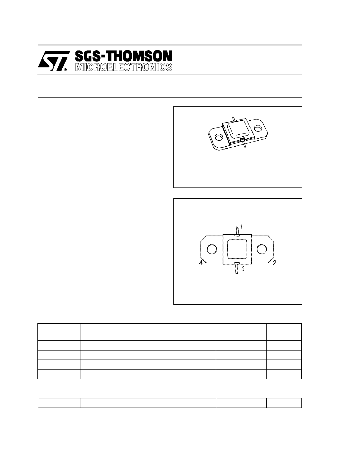
PIN CONNEC T IO N
1. Collector 3. Emitter
2. Base 4. Base
40 W
°
C
°
C
THERMA L DATA
RTH(j-c) Junction-Case Thermal Resistance 3.75
*Appliesonly to rated RFamplifier operation
August 1992
°
C/W
1/4
Page 2

AM82731-006
ELEC TRICAL SPECIFICA TI ONS (T
case
= 25°C)
STATIC
Symbol Test Condition s
BV
BV
BV
I
CES
h
CBO
EBO
CER
FE
C
I
= 5mA IE= 0mA 50 — — V
C
IE= 1mA IC= 0mA 3.5 — — V
IC= 5mA RBE= 10Ω 50 — — V
VCE= 30V — — 4 mA
VCE= 5V IC= 500mA 10 — — —
DYNAMIC
Symbol T est Conditions
P
OUT
η
C
G
PB
Note: Pulse Width
f = 2.7 — 3.1GHz P
f = 2.7 — 3.1GHz P
f = 2.7 — 3.1GHz P
100µS
=
Duty Cyc le=10%
1.5W V
IN =
1.5W V
IN =
1.5W V
IN =
Value
Min. Typ. Max.
Value
Min. Typ. Max.
30V 5.5 6.0 — W
CC =
30V 27 32 — %
CC =
30V 5.6 6.0 — dB
CC =
Unit
Uni t
TYPICAL PERFO RMAN CE
TYPICAL BROADBAND
PERFORMANCE
2/4
Page 3

IMPEDANCE DATA
TYPICAL INPUT
IMPEDANCES
Z
IN
AM82731-006
Z
IN
M
TYPICAL COLLECTOR
LOAD IMPEDANCES
Z
CL
FREQ. ZIN(Ω)Z
CL
L=2.7 GHz 9.0 + j 22.0 48.0 + j 11.5
2.9 GHz 9.0 + j 23.0 43.0 + j 9.0
=
•
M=3.1 GHz 12.5 + j 25.0 30.0 + j 3.0
3.3 GHz 20.0 + j 25.0 21.5 + j 0.0
=
•
H=3.5 GHz 22.0 + j 22.5 16.0 − j 3.0
TEST CIRCUIT
(Ω)
L
H
Z
CL
M
H
PIN= 1.5W
VCC= 30V
Normalized to 50 ohms
L
All dimensions are in inches.
Substrate material: .025 thick Al2O3(Er=9.6)
C1 : 1500 pF RF Feedthru
C2 : 100 µF Electrolytic
C3 : 100 pF Chip Capacitor
L1 : No. 32 Wire, 0.062 Inch Long
L2 : Printed RF Choke
3/4
Page 4

AM82731-006
PACKAGE MECHANICAL DATA
Information furnished is believed to be accurate and reliable. However, SGS-THOMSON Microelectronics assumes no responsability for the
consequences of use of such information nor for any infringement of patents or other rights of third parties which may results from its use. No
license is granted byimplication or otherwise under any patent or patent rights ofSGS-THOMSONMicroelectronics. Specificationsmentioned
in this publication are subject to change without notice. This publication supersedes and replaces all information previously supplied.
SGS-THOMSON Microelectronicsproductsare not authorizedforuse ascritical componentsin life supportdevices or systemswithout express
written approval of SGS-THOMSON Microelectonics.
1994 SGS-THOMSON Microelectronics - All Rights Reserved
Australia - Brazil - France - Germany - Hong Kong - Italy - Japan - Korea - Malaysia - Malta - Morocco - The Netherlands -
Singapore - Spain - Sweden - Switzerland - Taiwan - Thailand - UnitedKingdom - U.S.A
SGS-THOMSON Microelectronics GROUP OF COMPANIES
4/4
 Loading...