

Page 1
RF & MICROWAVE TRANSISTORS
.REFRACTORY/GOLD METALLIZATION
.EMITTER SITE BALLASTED
.
:1 VSWR CAPABILITY AT RATED
∞
CONDITIONS
.LOW THERMAL RESISTANCE
.INPUT/OUTPUT MATCHING
.OVERLAY GEOMETRY
.METAL/CERAMIC HERMETIC PACKAGE
.P
DESCRIPTION
The AM82223-010 is a common base, silicon
NPN bipolar transistor designed for high gain
and efficiency in the 2.2 − 2.3 GHz frequency
range.
Suitable for hi-rel aerospace telemetry applications, the AM82223-010 is provided in the industry-standard AMPAC™ metal/ceramic hermetic
package and incorporates internal input and output impedance matching structures along with a
rugged, emitter-site ballasted overlay die geometry.
= 9 W MIN. WITH 6.5 dB GAIN
OUT
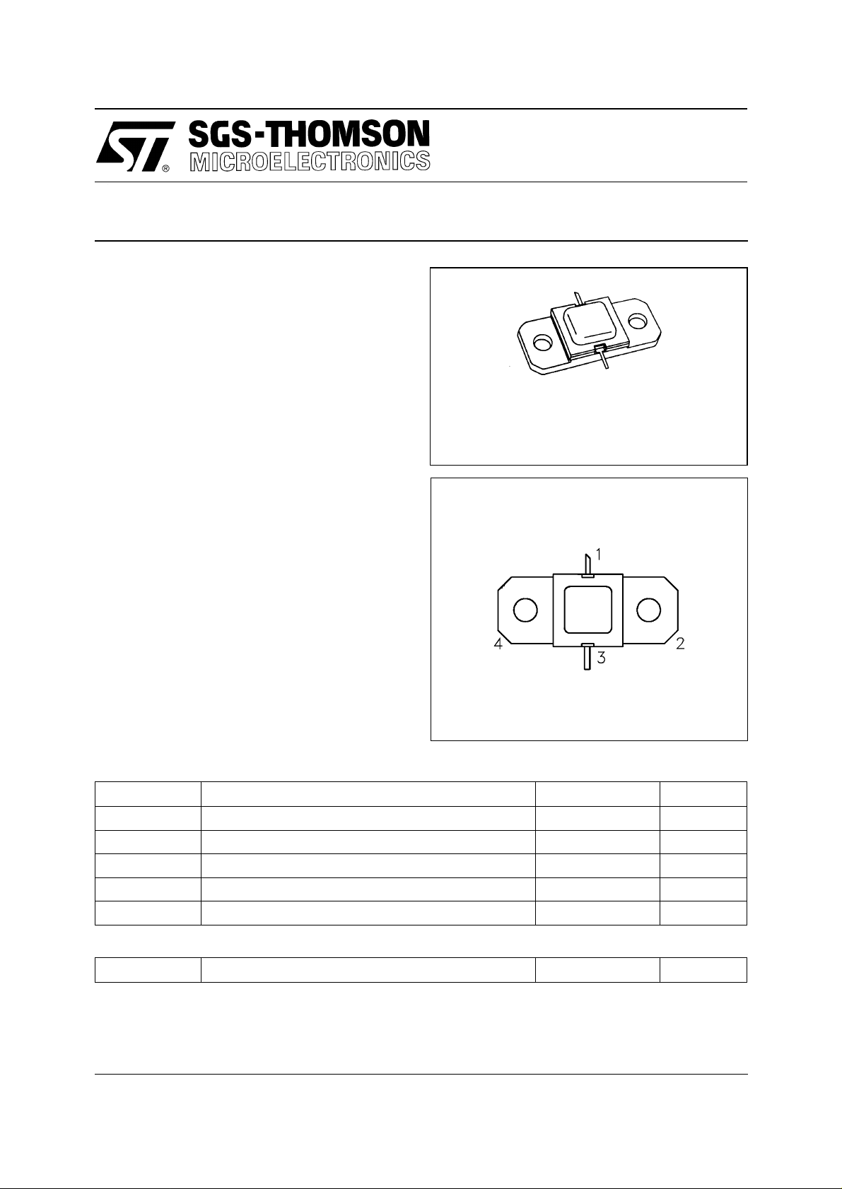
.400 x . 40 0 2NLFL (S042)
ORDER CO DE
AM82223-010
PIN CONNECTION
AM82223-010
TELEMETRY APPLICATIONS
hermetically sealed
BRANDING
82223-10
AM82223-010 is capable of withstanding ∞:1
load mismatch at any phase angle under full
rated operating conditions.
ABSOLUTE MAXIMUM RATINGS (T
Symbol Parameter Value Unit
P
DISS
I
C
V
CC
T
J
T
STG
THERMAL DATA
R
TH(j-c)
*Applies only to rated RF amplifier operation
NOTE: Thermal Resistance determined by Infra-Red Scanning of Hot-Spot
August 31, 1994
Junction Temperature at rated RF operating conditions.
Power Dissipation* (TC ≤ 75˚C) 28 W
Device Current* 1.2 A
Collector-Supply Voltage* 26 V
Junction Temperature 200
Storage Temperature
Junction-Case Thermal Resistance 4.4
case
= 25°C)
1. Collector 3. Emitter
2. Base 4. Base
65 to +200
−
°
°
°
C/W
C
C
1/3
Page 2
AM82223-010
ELECTRICAL SPECIFICATIONS (T
case
= 25°C)
STATIC
Symbol
BV
CBOIC
BV
CERIC
BV
EBOIE
I
CBO
h
FE
= 5 mA IE = 0 mA 45 — — V
= 10 mA RBE = 10 Ω 45 — — V
= 1 mA IC = 0 mA 3.5 — — V
VCB = 24 V — — 1 m A
VCE = 5 V IC = 750 mA 20 — 300 —
Test Condition s Value
Min. Typ. Max.
DYNAMIC
Symbol Test Conditi ons
P
OUT
η
P
f = 2.2 − 2.3 GHz PIN = 2.0 W VCC = 24 V 9.0 — — W
cf = 2.2 − 2.3 GHz PIN = 2.0 W VCC = 24 V 40 — — %
f = 2.2 − 2.3 GHz PIN = 2.0 W VCC = 24 V 6.5 — — dB
G
Value
Min. Typ. Max.
Unit
Unit
2/3
Page 3
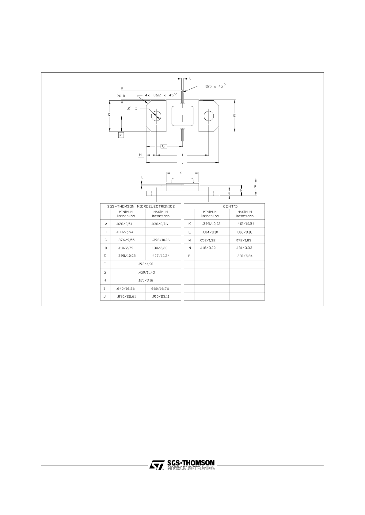
PACKAGE MECHANICAL DATA
Ref.: Dwg. No. 12-0213 rev. A
AM82223-010
Information furnished is believed to be accurate and reliable. However, SGS-THOMSON Microelectronics assumes no responsibility
for the cons equences of us e of such inform ation nor for any infri ngement of patents or other rights of third par ties which may re sul t
from its use. No lice nse is gr anted by impl icati on or otherw ise under any pate nt or patent rights of SGS-TH OMSON Mic roelect ronics.
Specifications mentioned in this publication are subject to change without notice. This publication supersedes and replaces all
informati on previo usly suppl ied. SGS-TH OMSON Microe lectronics products are not author ized for us e as critical c omponents in life
support devices or systems without express written approval of SG S-TH OMS ON Mic roelec t roni cs.
© 1994 SGS -TH OMSO N M icro elec tron ic s - All Ri ghts Rese rve d
Australia - Braz il - F rance - Ger man y - H ong Kon g - Ital y - Jap an - K orea - Ma lays ia - Malt a - Mor occ o - T he Nether lan ds -
Singapore - Spain - Sweden - Swit zerland - Taiwan - Thail and - United Ki ngdom - U.S.A .
SGS-THOMSON Microele ctronics GROUP OF C OMPANIES
3/3
 Loading...