

Page 1
RF & MICROWA VE TRANSIST ORS
.REFRACTORY/GOLD METALLIZATION
.EMITTER SITE BALLASTED
.LOW THERMAL RESISTANCE
.INPUT/OUTPUT MATCHING
.OVERLAY GEOMETRY
.METAL/CERAMIC HERMETIC PACKAGE
.P
OUT
DESC RIPT ION
The AM81719-030 is a high power silicon NPN
bipolar transistor designed for Class C, CW communications and telemetry applications in the 1.75
- 1.85 GHz frequency range.
An emitter site ballasted refractory/gold overlay
die geometry computerized automatic wirebonding
is employed to ensure long term reliability and
product consistency.
AM81719-030 is supplied in the industry-standard
AMPAC hermetic metal/ceramic package.
28 W MIN. WITH 6.7 dB GAIN
=
AM81719-030
TELEMETRY APPLICATIONS
PRELIMINARY DATA
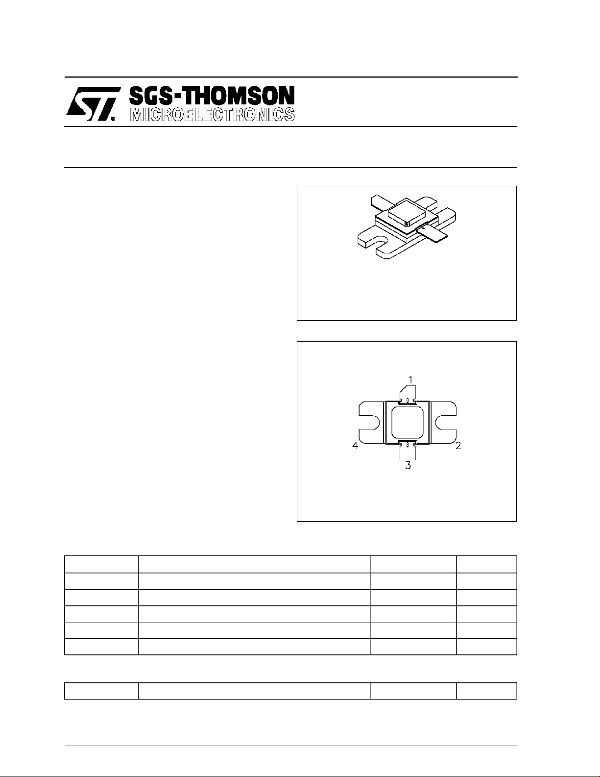
.400 SQ 2LFL (M147)
hermetically sealed
ORDER CODE
AM81719-030
PIN CONNE C TIO N
1. Collector 3. Emitter
2. Base 4. Base
BRAND I NG
81719-030
ABSOLUTE MAXIMUM RATINGS (T
Symbol Parameter Value Uni t
P
DISS
I
C
V
CC
T
J
T
STG
THERMA L DA TA
R
TH(j-c)
*Appliesonly to ratedRF amplifieroperation
September 1992
Power Dissipation* 67.3 W
Device Current* 2.67 A
Collector-Supply Voltage* 28 V
Junction Temperature 200
Storage Temperature − 65 to +200
Junction-Case Thermal Resistance* 2.6 °C/W
case
= 25°C)
°
C
°
C
1/4
Page 2
AM81719-030
ELECTRICAL SPECIF ICATIO NS (Tcase = 25°C)
STATIC
Symbol Test Conditions
BV
BV
BV
I
CES
h
CBO
EBO
CES
FE
IC= 10mA IE= 0mA 45 — — V
IE= 10mA IC= 0mA 3.0 — — V
IC = 10mA 45 — — V
VBE= 0V VCE= 28V — — 5 mA
VCE= 5V IC= 2mA 15 — 150 —
Min. Typ. Max.
DYNAMIC
Symbol Test Conditi ons
P
OUT
η
cf=1.75 — 1.85GHz PIN= 6.0W VCC= 28V 40 — — %
G
P
f = 1.75 — 1.85GHz PIN= 6.0W VCC= 28V 28 — — W
f = 1.75 — 1.85GHz PIN= 6.0W VCC= 28V 6.7 — — dB
Min. Typ. Max.
Value
Value
Unit
Unit
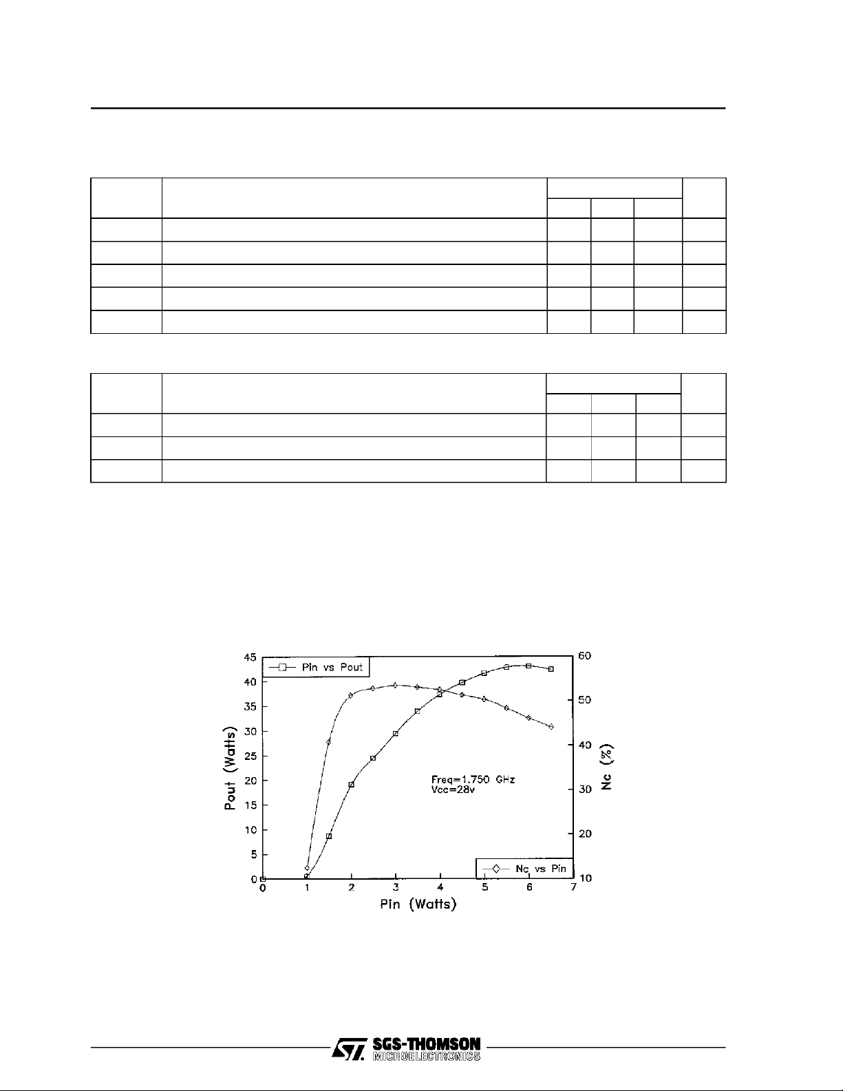
TYPICA L PERFO R MA NCE
POWER OUTPUT & CO LLECTOR
EFFICENCY vs POWER INPUT
2/4
Page 3

IMPEDA NCE DATA
TYPICAL INPUT
IMPEDANCE
Z
IN
TYPICAL COLLECTOR
LOAD IMPEDANCE
AM81719-030
Z
IN
L
H
Z
CL
H
Z
CL
FREQ. ZIN(Ω)Z
CL
L = 1.7 GHz 10.5 + j 16.0 2.5 − j 2.0
M = 1.8 GHz 10.25 + j 15.0 2.5 + j 0.0
H = 1.9 GHz 9.5 + j 14.5 2.5 + j 2.0
TEST CIRCUIT
Ref. Dwg. No. C125450A
All dimensions are in inches.
(Ω)
L
PIN= 6.0 W
VCC= 28 V
Normalized to 50 ohms
3/4
Page 4

AM81719-030
PACKAGE MECHANICAL DATA
Ref.: Dwg. No. 12-0147
Information furnished is believed to be accurate and reliable.However, SGS-THOMSON Microelectronics assumes no responsability for the
consequences of use of such information nor for any infringementofpatents or other rights of third parties which may results from its use. No
license isgranted by implication orotherwise underany patentor patent rights ofSGS-THOMSON Microelectronics. Specificationsmentioned
in this publication are subject to changewithout notice. This publication supersedes andreplaces all information previously supplied.
SGS-THOMSON Microelectronicsproductsare notauthorized foruse ascritical componentsinlife supportdevicesor systemswithout express
written approval of SGS-THOMSON Microelectonics.
1994 SGS-THOMSON Microelectronics - All RightsReserved
Australia - Brazil - France - Germany - Hong Kong - Italy - Japan - Korea - Malaysia - Malta - Morocco - The Netherlands -
Singapore - Spain - Sweden - Switzerland - Taiwan - Thailand - United Kingdom - U.S.A
SGS-THOMSON MicroelectronicsGROUP OF COMPANIES
4/4
 Loading...