

Page 1
RF & MICROWAVE TRAN SIST ORS
L-BAND RADAR APPLICAT IONS
.REFRACTORY/GOLD METALLIZATION
.EMITTER SITE BALLASTED
. 5: 1 VSWR CAPABILITY
. LOW THERMAL RESISTANCE
.INPUT/OUTPUT MATCHING
.O VERLAY GEOMETRY
.METAL/CERAMIC HERMETIC PACKAGE
.P
OUT
DESCRIPTION
The AM81214-015 device is a high power Class C
transistor specifically designed for L-Band Radar
pulsedoutput and driverapplications.
Thisdeviceiscapable ofoperation overa widerange
of pulse widths, duty cycles, and temperatures and
is capable of withstanding 5:1 output VSWRatrated
RF conditions. LowRF thermal resistance and computerized automaticwire bondingtechniques ensure
high reliability and product consistency.
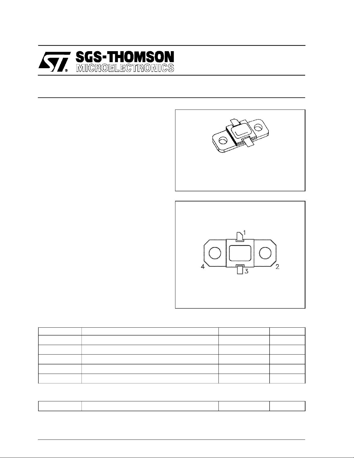
AM81214-015 is supplied in the grounded IMPAC
Hermetic Metal/Ceramic package with internal
input/output matching structures.
14.5 W MIN. WITH 8.6 dB GAIN
=
.310 x .310 2LF L ( S064)
ORDER CODE
AM 81214-015
PIN CONNE CTI ON
1. Collector 3. Emitter
2. Base 4. Base
AM81214-015
hermetically sealed
BRANDING
81214-15
ABSOLU TE MAXI MUM R AT ING S (T
Symbol Parameter Value Uni t
P
DISS
I
C
V
CC
T
J
T
STG
THERMA L DAT A
R
TH(j-c)
*Appliesonly torated RF amplifier operation
August 1992 1/4
Power Dissipation* (TC≤ 100°C) 37.5 W
Device Current* 1.8 A
Collector-Supply Voltage* 32 V
Junction Temperature (Pulsed RF Operation) 250
Storage Temperature − 65 to +200
Junction-Case Thermal Resistance* 4.0 °C/W
case
= 25°C)
°
C
°
C
Page 2
AM81214-015
ELEC TRICA L SPECIFICATIONS (T
case
= 25°C)
STATIC
Value
Symbol T est Cond itions
BV
BV
BV
I
CES
h
CBO
EBO
CER
FE
IC= 15mA IE= 0mA 48 — — V
IE= 1.5mA IC= 0mA 3.5 — — V
IC = 15mA RBE= 10Ω 48 — — V
VCE= 28V VBE= 28V — — 1.5 mA
VCE= 5V IC= 1A 30 — 300 —
Min. Typ. Max.
DYNAMIC
Value
Symbol T est Cond itions
P
IN
η
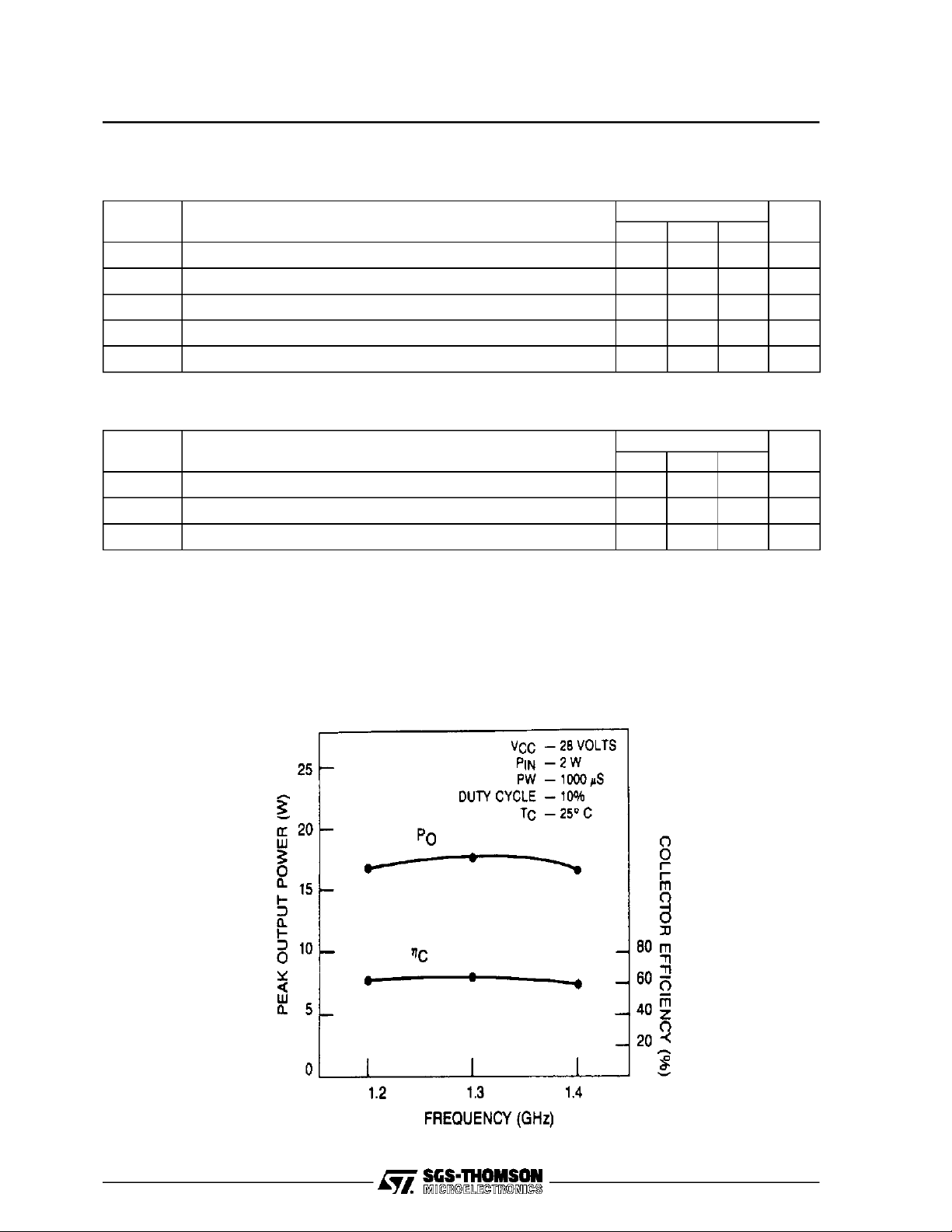
cf=1.2 — 1.4GHz PIN= 2W Peak VCC= 28V 48 58 — %
G
P
Note: Pulse Wi dth = 1000 µ S
f = 1.2 — 1.4GHz PIN= 2W Peak VCC= 28V 14.5 17.0 — W
f = 1.2 — 1.4GHz PIN= 2W Peak VCC= 28V 8.6 9.3 — dB
Duty Cycle = 10%
Min. Typ . Max.
Uni t
Unit
TYPICAL PERFORMAN CE
TYPICAL BROADBAND
PERFORMANCE
2/4
Page 3

IMPEDA NCE DATA
TYPICAL INPUT
IMPEDANCE
Z
IN
TYPICAL COLLECTOR
LOAD I MPEDANCE
AM81214-015
Z
CL
FREQ. ZIN(Ω)Z
L = 1.2 GHz 3.0 + j 6.5 16 + j 3.0
M = 1.3 GHz 3.5 + j 7.5 13 + j 6.0
H = 1.4 GHz 5.0 + j 7.0 11 + j 5.0
TEST CIRC UI T
CL
(Ω)
PIN= 2W
VCC= 28 V
Normalized to 50 ohms
3/4
Page 4

AM81214-015
PACKAGE MECHANICAL DATA
.318/
.306
Information furnished is believed tobe accurateand reliable.However, SGS-THOMSON Microelectronicsassumes no responsability for the
consequences of use of such information nor for any infringementof patents orother rights of third partieswhich mayresults from its use. No
license isgranted by implicationor otherwise underany patent or patentrights of SGS-THOMSON Microelectronics.Specificationsmentioned
in this publication are subject to changewithout notice. This publication supersedes and replaces all information previously supplied.
SGS-THOMSON Microelectronicsproductsare notauthorizedforuse ascritical componentsin lifesupport devicesor systemswithout express
written approval of SGS-THOMSON Microelectonics.
1994 SGS-THOMSON Microelectronics - All RightsReserved
Australia - Brazil - France - Germany- HongKong - Italy - Japan - Korea - Malaysia - Malta -Morocco - The Netherlands-
Singapore - Spain - Sweden - Switzerland - Taiwan - Thailand - UnitedKingdom - U.S.A
SGS-THOMSON MicroelectronicsGROUP OF COMPANIES
4/4
 Loading...