

Page 1
RF & MICROWAVE TRANSISTORS
L-BAND RADAR APPLICATION S
.310 x .310 2LFL (S064)
hermetically sealed
.REFRACTORY/GOLD METALLIZATION
.EMITTER SITE BALLASTED
.5:1 VSWR CAPABILITY
.LOW THERMAL RESISTANCE
.INPUT/OUTPUT MATCHING
.OVERLAY GEOMETRY
.METAL/CERAMIC HERMETIC PACKAGE
.P
OUT
=
5.5 W MIN. WITH 10 dB GAIN
DESCRI P TI ON
The AM81214-006 device is a high power Class
C transistor specifically designed for L-Band Radar pulsed driver applications.
This device is capable of operation over a wide
range of pulse widths, duty cycles, and temperatures and is capable of withstanding 5:1 output
VSWR at rated RF conditions. Low RF thermal
resistance an d compute rized automatic wire
bonding techniques ensure high reliability and
product consistency.
AM81214-006 is supplied in the grounded IMPAC Hermetic Metal/Ceramic package with internal input/output matching structures.
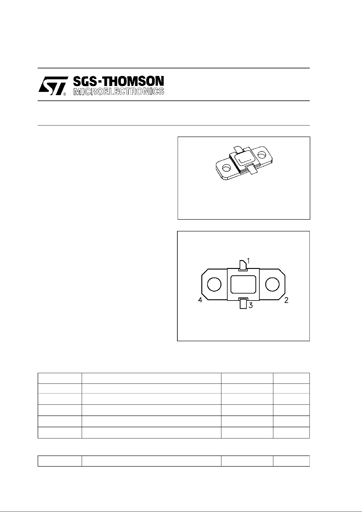
PIN CONNECTI ON
BRANDI NG
81214-6
ORDER CODE
AM81214-6
ABSOLUTE MAXIM UM RATINGS (T
case
= 25°C)
Symbol Parameter Value Unit
P
DISS
Power Dissipation* (TC≤ 100°C)
16.7 W
I
C
Device Current* 0.82 A
V
CC
Collector-Supply Voltage* 32 V
T
J
Junction Temperature (Pulsed RF Operation) 250
°
C
T
STG
Storage Temperature
− 65 to +200
°
C
R
TH(j-c)
Junction-CaseThermal Resistance* 9.0 °
C/W
*Appliesonly to rated RF amplifieroperation
AM81214-006
1. Collector 3. Emitter
2. Base 4. Base
THERMAL DATA
Page 2
ELECTRICAL S PEC I FICATIO NS (T
case
= 25°C)
Symbol Test Conditions
Value
Uni t
Min. Typ. Max.
P
OUT f = 1.2 — 1.4 GHz P
IN
= 0.5 W VCC= 28 V
— 5.5 6.2 W
η
cf=1.2 — 1.4 GHz P
IN
= 0.5 W VCC= 28 V
47 52 — %
G
P f = 1.2 — 1.4 GHz P
IN
= 0.5 W VCC= 28 V
10 10.5 — dB
Note: P ulse Width = 1000µS
Duty Cycle = 10%
STATIC
Symbol Test Conditions
Value
Uni t
Min. Typ. Max.
BV
CBO
IC= 1mA IE=0mA
48 — — V
BV
CER
IC= 5mA RBE= 10Ω
48 — — V
BV
EBO
IE= 1mA IC=0mA
3.5 — — V
I
CES
VBE= 0V VCE= 28 V
——500
µA
h
FE
VCE= 5V IC=500 mA
15 — 300 —
DYNAMIC
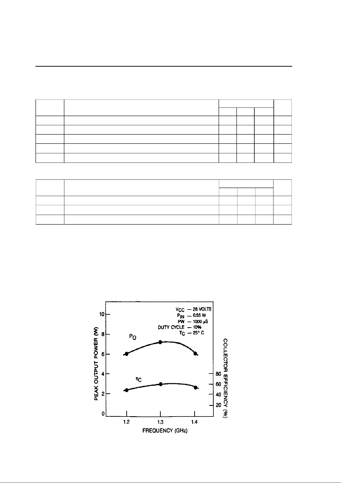
TYPICAL PERFOR MANCE
TYPICAL BROADBAND
PERFORMANCE
AM8 1214-006
Page 3

TEST CIRCUI T
All dimensions are in inches.
Substrate material: .025 thick AI
2O3
C1 : 0.2—2.5 pF Johanson Gigatrim Capacitor
C2 : 0.2—2.5 pF Johanson Gigatrim Capacitor
C3 : 1500 pF Filtercon Feedthrough
C4 : 0.1 µF, Ceramic Capacitor
C5 : 100 µF, Electrolytic Capacitor
C6 : 100 pF Chip Capacitor
L : No. 26 Wire, 4 Turn .062 I.D.
PIN= 0.5 W
V
CC
= 28 V
Normalized to 50 ohms
IMPEDANCE DATA
Z
IN
TYPICAL INPUT
IMPEDANCE
Z
CL
TYPICAL COLLECTOR
LOAD IMPEDANCE
FREQ.
Z
IN
(Ω)Z
CL
(Ω)
L = 1.2 GHz
10.5 + j 9.0 9.0 + j 3.0
M = 1.3 GHz
9.5 + j 8.0 6.5 + j 2.0
AM8 1214-006
Page 4

PACKAGE MECHANI CAL DATA
Ref.: Dwg. No. 12-0221 rev. A
Information furnished is believed to be accurate and reliable. However, SGS-THOMSON Microelectronics assumes no responsibility
for the consequences of use of such information nor for any infringement of patents or other rights of third parties which may result
from its use. No license is granted by implication or otherwise under any patent or patent rights of SGS-THOMSON Microelectronics. Specifications mentioned in this publication are subject to change without notice. This publication supersedes and replaces all
information previously supplied. SGS-THOMSON Microelectronics products are not authorized for use as critical components in life
support devices or systems without express written approval of SGS-THOMSON Microelectronics.
1995 SGS-THOMSON Microelectronics - All Rights Reserved
SGS-THOMSON Microelectronics GROUP OF COMPANIES
Australia - Brazil - France - Germany - Hong Kong - Italy - Japan - Korea - Malaysia - Malta - Morocco - The Netherlands -
Singapore - Spain - Sweden - Switzerland - Taiwan - Thailand - United Kingdom - U.S.A.
AM8 1214-006
 Loading...