

Page 1
RF & MICROWAVE TRANSISTORS
SPECIA LITY AVIONIC S/JTI DS APPLICAT IONS
.REFRACTORY/GOLD METALLIZATION
.EMITTER SITE BALLASTED
. 15: 1 VSWR CAPABILITY
. LOW RF THERMAL RESISTANCE
.INPUT/OUTPUT MATCHING
.O VERLAY GEOMETRY
.METAL/CERAMIC HERMETIC PACKAGE
.P
OUT
30 W MIN. WITH 7.8 dB GAIN
=
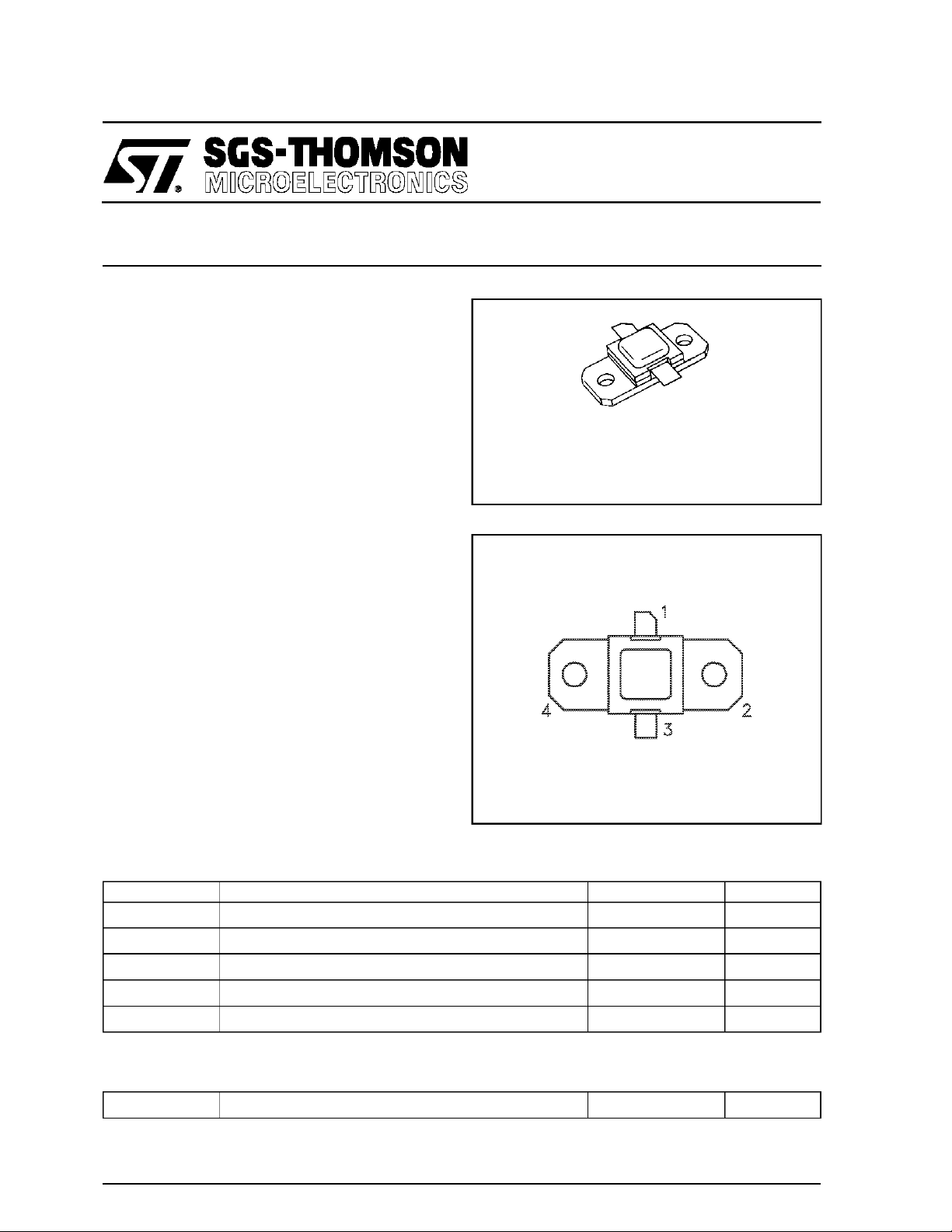
.400 x .400 2LFL (S036)
hermetically sealed
ORDER CODE
AM80912-030
AM80912-030
BRAND I NG
80912-30
DESCRIPT I ON
The AM80912-030 device is a high power Class C
transistorspecifically designedforJTIDS pulsedoutput anddriverapplications.
Thisdeviceis capable ofoperation over a widerange
of pulse widths, duty cycles and temperatures and is
capable of withstanding 15:1 output VSWR at rated
RF conditions.
Low RF thermal resistance and computerized automaticwirebonding techniques ensure high reliability
and product consistency.
The AM80912-030 is supplied in the hermetic metal/ceramic package with internal input matching
structures.
ABSOLU TE MAXI MUM RATING S (T
Symbol Parameter Value Uni t
P
T
DISS
I
V
CC
T
STG
C
J
Power Dissipation* (TC≤ 85°C) 75 W
Collector Current* 3.5 A
Collector-Supply Voltage* 40 V
Junction Temperature (Pulsed RF Operation) 250
Storage Temperature − 65 to +200
case
= 25°C)
PIN CONNECTION
1. Collector 3. Emitter
2. Base 4. Base
°
C
°
C
THERMA L DAT A
R
TH(j-c)
*Appliesonly to rated RFamplifieroperation.
August 1992
Junction-Case Thermal Resistance 2.2 °C/W
1/6
Page 2
AM80912-030
ELEC TRICAL SPECIF ICA TIONS (T
case
25° C)
=
STATIC
Symbol Test Condition s
BV
BV
BV
I
CES
h
CBO
EBO
CER
FE
IC= 10mA 55 — — V
I
1mA 3.5 — — V
=
E
I
20mA R
=
C
V
35V — — 5.0 mA
=
CE
V
5V I
=
CE
10Ω 55 — — V
=
BE
1.0A 15 — 150 —
=
C
DYNAMIC
Symbol Test Condition s
P
OUT
η
C
G
P
Note: Pulse fo rmat: 6.4 µson6.6µs off, repeat f or 3. 3 ms, then of f for 4.5125 ms.
f=960 — 1215MHz P
f = 960 — 1215MHz P
f=960 — 1215MHz P
Duty Cycle: Burst 49.2%, over all 20.8%
IN
IN
IN =
5.0W V
=
5.0W V
=
5.0W V
+35V 30 36 — W
=
CC
+35V 40 45 — %
=
CC
+35V 7.8 8.6 — dB
CC =
Value
Min. Typ. Max.
Value
Min. Typ . Max.
Unit
Unit
2/6
Page 3

TYPICAL PERFORMAN CE
AM80912-030
TYPI CAL BROADBAND
POWER AMPLIFIER
TYPICAL RELATIVE POWER
OUTPUT & COLLECTOR
EFFICIENCY* vs CO LLECTOR
VOLTAGE
MAXIMUM THERMAL RESISTANCE vs PULSE
WIDTH & DUTY CYCLE
DC=20%
DC=4%
Θjc (°C/W)
P
5W
=
IN
V
35 V
=
CC
T
40°C
=
C
PULSE WIDTH (µsec)
3/6
Page 4

AM80912-030
IMPEDA NCE DATA
TYPICAL INPUT
IMPEDANCE
Z
IN
P
5W
=
IN
V
+35V
=
CC
ZO*=50Ω
L=960 MHz 4.5 + j 6.0 11.0 − j 0.5
M=1090 MHz 5.5 + j 6.3 12.0 − j 2.0
H=1215 MHz 5.0 + j 5.0 12.5 − j 5.0
TYPICAL COLLECTOR
LOAD IMPEDANCE
Z
CL
P
5W
=
IN
V
+35V
=
CC
ZO*=50Ω
FREQ. ZIN(Ω)Z
CL
(Ω)
4/6
*Normalized Impedance
Page 5

TEST CIRCUIT
AM80912-030
PACKAGE MECHANICAL DATA
5/6
Page 6

AM80912-030
Information furnished is believed tobe accurateand reliable.However, SGS-THOMSONMicroelectronicsassumes no responsability for the
consequences of use of such information nor for any infringementof patents orother rights of thirdparties which mayresults from its use. No
license isgranted by implication orotherwise underany patentor patentrights of SGS-THOMSON Microelectronics.Specificationsmentioned
in this publication are subject to changewithout notice. This publication supersedes and replaces all information previously supplied.
SGS-THOMSON Microelectronicsproductsare notauthorized foruse ascritical componentsinlife supportdevices orsystems withoutexpress
written approval of SGS-THOMSON Microelectonics.
1994 SGS-THOMSON Microelectronics - All RightsReserved
Australia - Brazil - France - Germany- HongKong - Italy- Japan - Korea - Malaysia - Malta - Morocco - The Netherlands-
Singapore - Spain - Sweden - Switzerland - Taiwan - Thailand - UnitedKingdom - U.S.A
SGS-THOMSON MicroelectronicsGROUP OF COMPANIES
6/6
 Loading...