

Page 1
RF & MICROWAVE TRANSISTORS
.REFRACTORY/GOLD METALLIZATION
.EMITTER SITE BALLASTED
.
:1 VSWR CAPABILITY
∞
. LOW THERMAL RESISTANCE
.INPUT MATCHING
.METAL/CERAMIC HERMETIC PACKAGE
.P
= 15 W MIN. WITH 8.1 dB GAIN
OUT
.BANDWIDTH 255 MHz
AM80912-015
AVIONI CS APPLICA TIONS
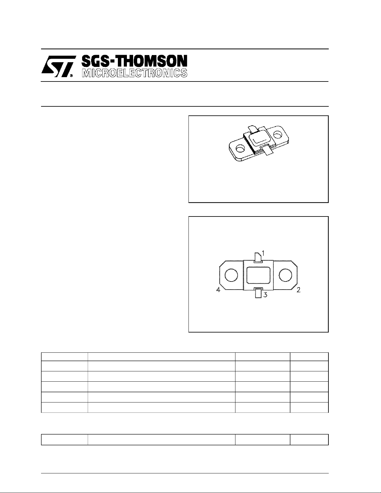
.310 x .3 10 2LF L (S064)
hermetically sealed
ORDER CODE
AM80912-015
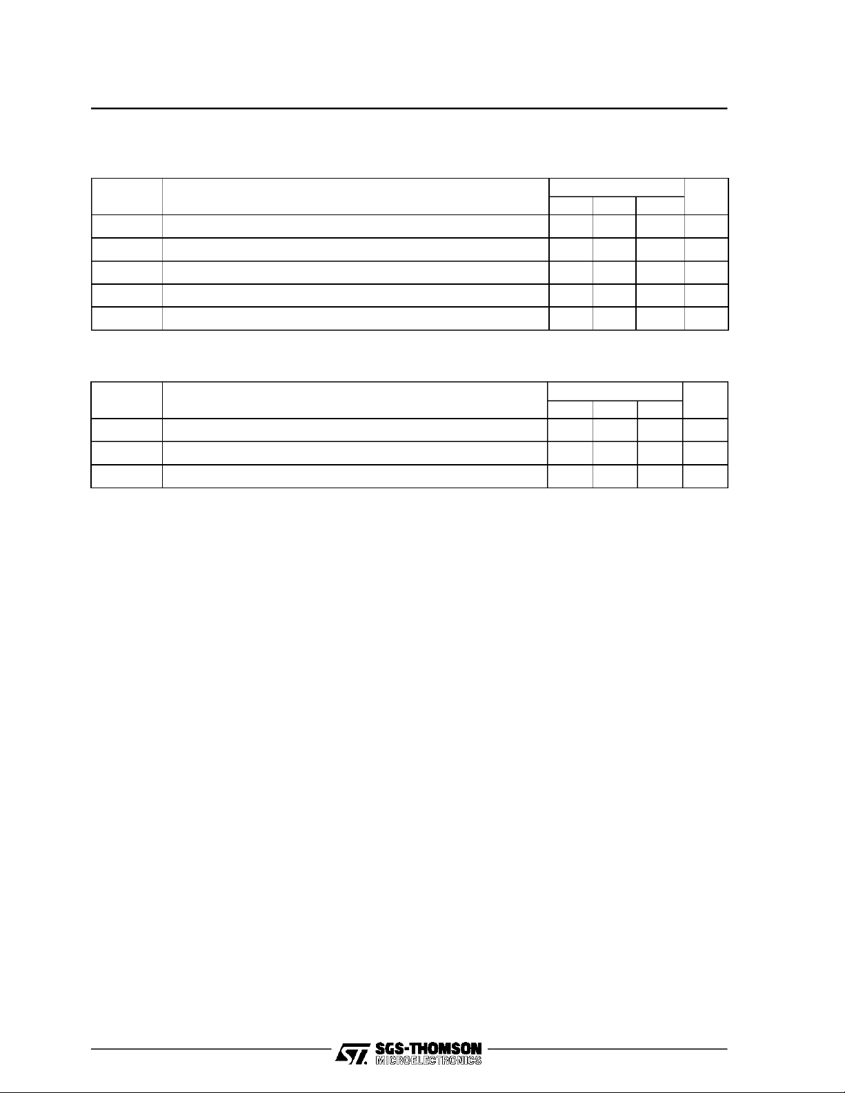
PIN CONNE C TIO N
DESCRIPTION
The AM80912-015 is designed for specialized
avionics applicati ons , including JTIDS, where
power is provided under pulse formats utilizing
short pulse widths and high burst or overall duty
cycles.
The AM80912-015 is housed in the unique
IMPAC Hermetic Metal/Ceramic package with
ABSOLU TE MAXI MUM R AT ING S (T
Symbol Parameter Value Uni t
P
T
DISS
I
V
CC
T
STG
C
J
Power Dissipation*(TC≤ 100°C) 50 W
Device Current* 1.8 A
Collector-Supply Voltage* 32 V
Junction Temperature (Pulsed RF Operation) 250
Storage Temperature − 65 to +200
case
= 25°C)
1. Collector 3. Emitter
2. Base 4. Base
BRAN DI NG
80912-15
°
C
°
C
THERMA L DAT A
R
TH(j-c)
*Appliesonly torated RFamplifier operation
March 1994
Junction-Case Thermal Resistance* 3.0 °C/W
1/6
Page 2
AM80912-015
ELEC TRICA L SPECIFICATIONS (T
case
= 25°C)
STATIC
Symbol Test Condi tion s
BV
BV
BV
I
CES
h
CBO
EBO
CER
FE
IC= 10mA IE= 0mA 55 — — V
IE= 1mA IC= 0mA 3.5 — — V
IC = 10mA RBE= 10Ω 55 — — V
VBE= 0V VCE= 28V — — 2.0 mA
VCE= 5V IC= 500mA 15 — 150 —
DYNAMIC
Symbol Test Conditions
P
OUT
η
cf=960 — 1215MHz P
G
P
Note: Pulse format: 6.4 µSon6.6µS off, repeat for 3.3 ms, t hen off for 4. 5125 ms.
f = 960 — 1215MHz P
f = 960 — 1215MHz P
Duty Cycle: Burs t 49.2%, overall 20.8%
IN
IN
IN
2.3W V
=
2.3W V
=
2.3W V
=
28V 15 17 — W
=
CC
28V 45 49 — %
=
CC
28V 8.1 8.9 — dB
=
CC
Value
Min. Typ. Max.
Value
Min. Typ. Max.
Unit
Unit
2/6
Page 3

TYPICAL PERFORMAN CE
TYPICAL BROADBAND
POWER AMPLIFIER
AM80912-015
RELATIVE POWER OUTPUT &
COLLECTOR EFFICIENCY vs
COLLECTOR VOLTAGE
MAXIMUM THERMAL RESISTANCE vs PULSE WIDTH & DUTY CYCLE
3/6
Page 4

AM80912-015
IMPEDA NCE DATA
TYPICAL INPUT
IMPEDANCE
Z
IN
PIN= 2.3 W
VCC= 28 V
ZO* = 50 ohms
FREQ. ZIN(Ω)Z
L = 960 MHz 5.7 + j 4.3 5.7 + j 7.7
M = 1090 MHz 5.8 + j 2.5 4.3 + j 6.5
H = 1215 MHz 5.0 + j 3.0 4.0 + j 4.8
TYPICAL COLLECTOR
LOAD IMPEDANCE
Z
CL
PIN= 2.3 W
VCC= 28 V
ZO* = 50 ohms
*Normalized Impedance
CL
(Ω)
4/6
Page 5

TEST CIRCUIT
Ref.: Dwg. No. 104-000284
AM80912-015
5/6
Page 6

AM80912-015
PACKAGE MECHANI CAL DATA
Ref.: Dwg. No. 12-221
Information furnished is believed tobe accurate and reliable. However, SGS-THOMSON Microelectronics assumes no responsability for the
consequences of use of such information nor for any infringementof patents or other rights of third parties which mayresults from its use. No
license isgranted by implicationor otherwise underany patent or patentrights of SGS-THOMSON Microelectronics. Specificationsmentioned
in this publication are subject to changewithout notice. This publication supersedes and replaces all information previously supplied.
SGS-THOMSON Microelectronicsproductsare notauthorizedforuse ascritical componentsin life support devicesor systemswithout express
written approval of SGS-THOMSON Microelectonics.
1994 SGS-THOMSON Microelectronics - All RightsReserved
Australia - Brazil - France - Germany - HongKong - Italy - Japan - Korea - Malaysia - Malta - Morocco - The Netherlands -
Singapore - Spain - Sweden - Switzerland - Taiwan - Thailand - UnitedKingdom - U.S.A
SGS-THOMSON MicroelectronicsGROUP OF COMPANIES
6/6
 Loading...