

Page 1

■
■
■
■
■
■
■
■
■
■
■
■
■
PRELIMINARY
Am79C989
Quad Ethernet Switching Transceiver (QuEST™)
DISTINCTIVE CHARACTERISTICS
Four independent 10BASE-T transceivers
compliant with the IEEE 802.3 standard
Four digital Manchester Encode/Decode
(MENDEC) units
On-chip filtering enables FCC EMI compliance
without external filters or common mode
chokes
Automatic polarity Correction and Detection on
10BASE-T receivers
Optional Attachment Unit Interface (AUI) for
non-10BASE-T transceivers
10BASE-T Extended Distance option
accommodate lines longer than 100 meters
Quad AMD Switching Interface (QuASI™)
interface reduces overall pin count
Half-Duplex and Full-Duplex operation
Auto-Negotiation compliant with IEEE 802.3u
Standard
Standard MII management interface and
protocol
Status Change Interrupt output pin for fast
response time to changed conditions
44-pin PLCC CMOS device
5 V supply with 3.3 V system interface
compatibility
GENERAL DESCRIPTION
The Am79C989 Quad Ethernet Switching Transceiver
(QuEST™) is a four-port physical layer (PHY) device
that provides all of the analog functions needed for a
10BASE-T switch, including four independent
Manchester Encode/Decode units (MENDECs) and
four independent 10BASE-T transceivers. If the AUI
port is used for a 10BASE-2, 10BASE-5, or
10BASE-FL transceiver, one of the four 10BASE-T
ports is disabled.
The QuEST device is designed for 10 Mbps Ethernet
switching hubs, port switching repeater hubs, routers,
bridges, and servers that require data encoding and
clock recovery on a per port basis and are limited by pin
constraints. Clock recovery is performed as par t of the
MENDEC function. The QuEST device supports every
physical layer function of a full-featured switch, including full-duplex operation with Auto-Negotiation and the
ability to use various media types.
A unique feature of the QuEST device is the Quad AMD
Switching Interface (QuASI) which multiplex es the data
for all four channels into one set of pins . This minimizes
the pin count and size of the QuEST device and substantially reduces overall system cost.
The QuEST device provides a 2-pin Media Independent Interface (MII) Management Interface which supports the protocols specified in the IEEE 802.3u
standard. Controlled by the switch system, this interface allows the QuEST de vice to be polled for status information and allows operating parameters of the
QuEST device, such as extended distance operation,
to be altered.
The Am79C989 device provides an Interrupt pin to indicate changes in the internal status of the device. The
interrupt function reduces CPU polling of status registers and allows fast response time to changes in physical layer conditions.
This document contains information on a product under development at Advanced Micro Devices. The information
is intended to help you evaluate this product. AMD reserves the right to change or discontinue work on this proposed
product without notice.
Publication# 21173 Rev: B Amendment/+2
Issue Date: April 1997
Page 2
PRELIMINARY
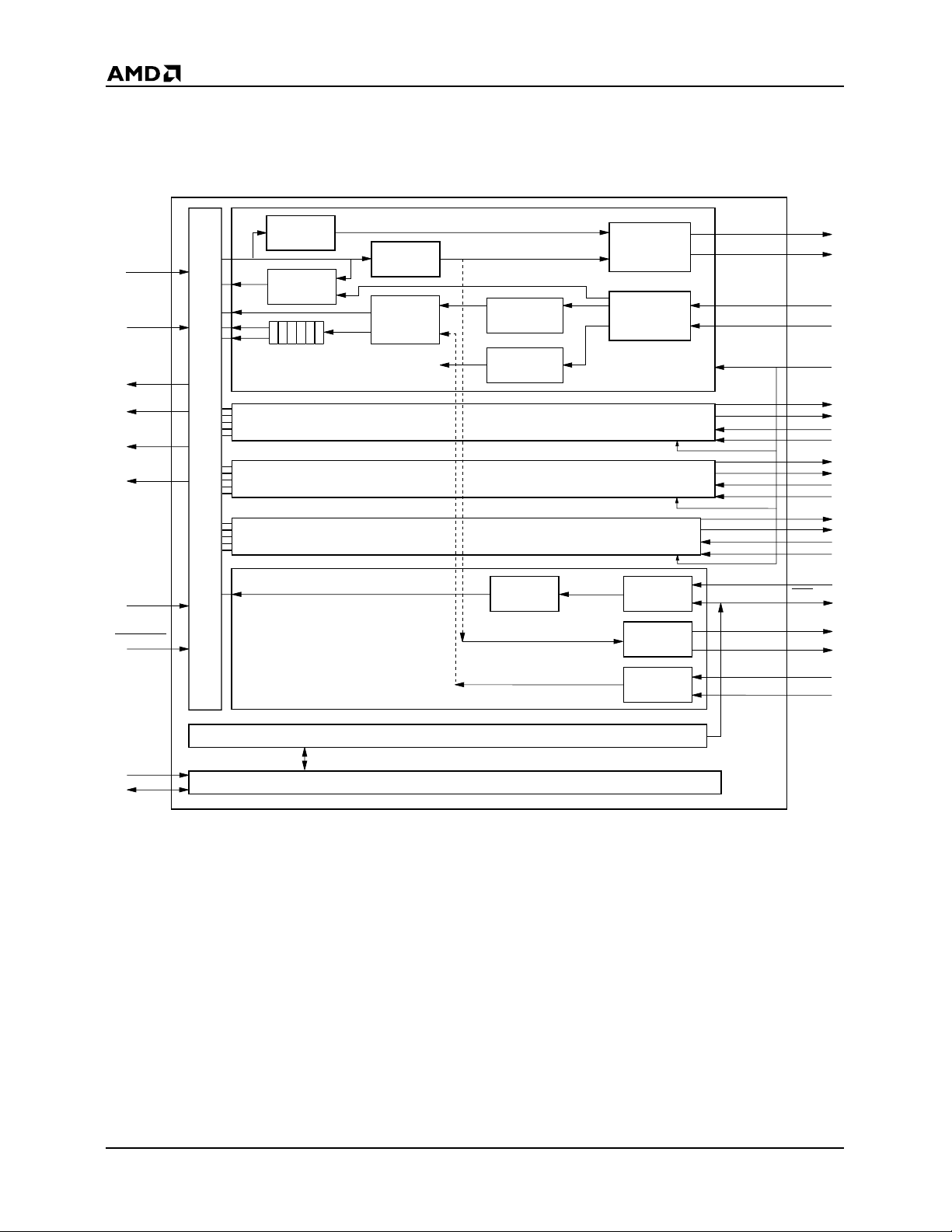
BLOCK DIAGRAM
System Interface Network Interface
QTX_EN
QTX_DATA
QRX_DATA
QRX_VALID
QRX_CRS
QCLSN
SCLK
QRST/STRB
QuASI Interface
Jabber
Timer
Collision
Detect
Elasticity FIFO
Manchester
Encoder
Manchester
Decode and
Carrier Detect
Link Detect
10BASE-T Transceiver 0
Polarity Detection/
Correction
Link/Auto Neg
State Machine
10BASE-T Transceiver 1
10BASE-T Transceiver 2
10BASE-T Transceiver 3
Collision
Attachment Unit Interface
Detect
Line Driver with
Wave Shaping
Line Receiver with
Smart Squelch
AUI Collision
Squelch
AUI Transmitter
AUI Receiver
with Squelch
TXD0+
TXD0-
RXD0+
RXD0-
REXT
TXD1+
TXD1-
RXD1+
RXD1-
TXD2+
TXD2-
RXD2+
RXD2-
TXD3+
TXD3-
RXD3+
RXD3-
PCI/CI+
QINT/CI-
DO+
DO-
DI+
DI-
Register Block
MDC
MDIO
v3
Management Interface
2 Am79C989
21173B-1
Page 3

PRELIMINARY
CONNECTION DIAGRAM
SCLK
QTX_EN
QTX_DATA
QRX_VALID
QRX_DATA
VDDIO
VSSIO
QRX_CRS
QCLSN
MDIO
MDC
QRST/STRB
REXT
VSS
QINT/CI-
PCI/CI+
DI-
DI+
VSSAUI
DO-
DO+
VDDTX
3
2
QuEST
Am79C989
44 PLCC
Version 2.0
23
22
TXD+
TXD1-
1
44
24
VDDTX
43
25
TXD2-
TXD2+
5
641
4
7
8
9
10
11
12
13
14
15
16
17
19
20
TXD0+
VSSTX
21
18 27
TXD0-
42
26
VSSTX
40
39
38
37
36
35
34
33
32
31
30
29
28
TXD3-
TXD3+
VDD
RXD3+
RXD3-
RXD2+
RXD2-
VSSRX
RXD1+
RXD1-
RXD0+
RXD0-
VDDTX
21173B-2
Am79C989 3
Page 4
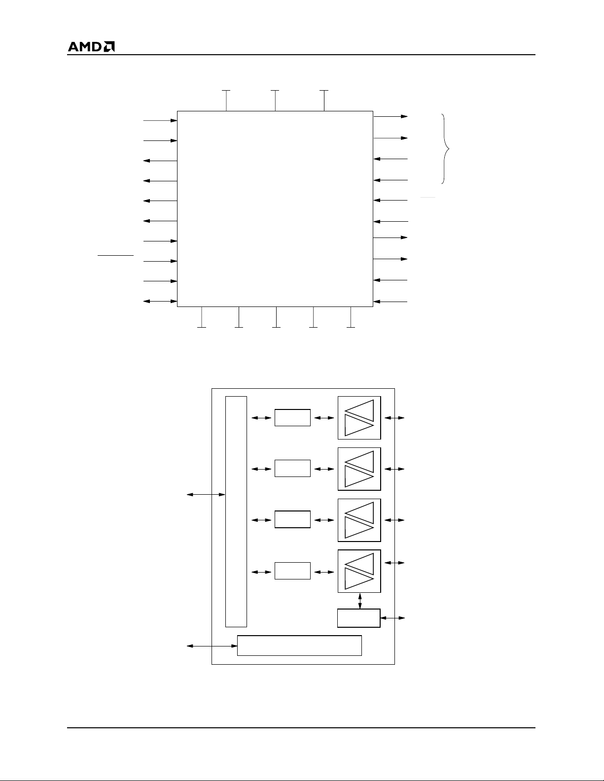
LOGIC DIAGRAM
PRELIMINARY
QTX_EN
QTX_DATA
QRX_DATA
QRX_VALID
QRX_CRS
QCLSN
SCLK
QRST/STRB
MDC
MDIO
LOGIC SYMBOL
V
DDIO
V
SS
V
SSAUI
V
DDTX(3)
V
SSTX(2)
V
SSRX
V
DD
V
SSIO
TXD+
TXD-
RXD+
RXD-
QINT/CI-
PCI/CI+
DO+
DO-
DI+
DI-
Twisted Pair Ports
(4 Ports)
21173B-3
QuASI
QuASI Interface
Management Interface
MENDEC
MENDEC
MENDEC
MENDEC
TP
TP
TP
TP
AUI
21173B-4
4 Am79C989
Page 5

RELATED PRODUCTS
PRELIMINARY
Part No.
Am7990
Am7992B Serial Interface Adapter (SIA)
Am7996 IEEE 802.3/Ethernet/Cheapernet Transceiver
Am79C90 CMOS Local Area Network Controller for Ethernet (C-LANCE)
Am79C98 Twisted Pair Ethernet Transceiver (TPEX)
Am79C100 Twisted Pair Ethernet Transceiver Plus (TPEX+)
Am79C870 Quad Fast Ethernet Transceiver (QFEX™) for 100BASE-X
Am79C871 Quad Fast Ethernet Transceiver for 100BASE-X Repeater (QFEXr™)
Am79C981 Integrated Multiport Repeater Plus (IMR+™)
Am79C982 basic Integrated Multiport Repeater (bIMR™)
Am79C983 Integrated Multiport Repeater 2 (IMR2™)
Am79C984A enhanced Integrated Multiport Repeater (eIMR™)
Am79C985 enhanced Integrated Multiport Repeater Plus (eIMR+™)
Am79C987 Hardware Implemented Management Information Base (HIMIB™)
Am79C988 Quad Integrated Ethernet Transceiver (QuIET™)
Am79C900 Integrated Local Area Communications Controller (ILACC™)
Am79C940 Media Access Controller for Ethernet (MACE™)
Am79C960 PCnet™-ISA Single-Chip Ethernet Controller (for ISA bus)
Am79C961 PCnet™-ISA+ Single-Chip Ethernet Controller for ISA (with Microsoft® Plug n’ Play® Support)
Am79C961A PCnet™-ISA II Full Duplex Single-Chip Ethernet Controller for ISA
Am79C965 PCnet™-32 Single-Chip 32-Bit Ethernet Controller
Am79C970 PCnet™-PCI Single-Chip Ethernet Controller (for PCI bus)
Am79C970A PCnet™-PCI II Full Duplex Single-Chip Ethernet Controller (for PCI bus)
Am79C971B PCnet™Am79C974 PCnet™-SCSI Combination Ethernet and SCSI Controller for PCI Systems
Local Area Network Controller for Ethernet (LANCE)
FAST
Single-Chip Full-Duplex 10/100 Mbps Ethernet Controller for PCI Local Bus
Description
Am79C989 5
Page 6
PRELIMINARY
ORDERING INFORMATION
Standard Products
AMD standard products are available in se ver al packages and operating r anges. The order number (V alid Combination) is formed
by a combination of the elements below.
Am79C989
J
C
ALTERNATE PACKAGING OPTION
\T = Tape and reel
TEMPERATURE RANGE
C = Commercial (0˚C to +70˚C)
P ACKA GE TYPE
J = 44 PLCC
Valid Combinations
Am79C989 JC or JC\T
SPEED OPTION
Not Applicable
DEVICE NUMBER/DESCRIPTION
Am79C989
Quad Ethernet Switching Transceiver (QuEST)
Valid Combinations
Valid Combinations list configurations planned to be supported in volume for this device. Consult the local AMD sales
office to confirm availability of specific valid combinations and
to check on newly released combinations.
6 Am79C989
Page 7

PRELIMINARY
TABLE OF CONTENTS
DISTINCTIVE CHARACTERISTICS . . . . . . . . . . . . . . . . . . . . . . . . . . . . . . . . . . . . . . . . . . . . . . . . . . 1
GENERAL DESCRIPTION . . . . . . . . . . . . . . . . . . . . . . . . . . . . . . . . . . . . . . . . . . . . . . . . . . . . . . . . . 1
BLOCK DIAGRAM . . . . . . . . . . . . . . . . . . . . . . . . . . . . . . . . . . . . . . . . . . . . . . . . . . . . . . . . . . . . . . . 2
CONNECTION DIAGRAM. . . . . . . . . . . . . . . . . . . . . . . . . . . . . . . . . . . . . . . . . . . . . . . . . . . . . . . . . . 3
LOGIC DIAGRAM . . . . . . . . . . . . . . . . . . . . . . . . . . . . . . . . . . . . . . . . . . . . . . . . . . . . . . . . . . . . . . . . 4
LOGIC SYMBOL . . . . . . . . . . . . . . . . . . . . . . . . . . . . . . . . . . . . . . . . . . . . . . . . . . . . . . . . . . . . . . . . . 4
RELATED PRODUCTS. . . . . . . . . . . . . . . . . . . . . . . . . . . . . . . . . . . . . . . . . . . . . . . . . . . . . . . . . . . . 5
ORDERING INFORMATION . . . . . . . . . . . . . . . . . . . . . . . . . . . . . . . . . . . . . . . . . . . . . . . . . . . . . . . . 6
Standard Products. . . . . . . . . . . . . . . . . . . . . . . . . . . . . . . . . . . . . . . . . . . . . . . . . . . . . . . . . . . . . 6
PIN DESIGNATIONS. . . . . . . . . . . . . . . . . . . . . . . . . . . . . . . . . . . . . . . . . . . . . . . . . . . . . . . . . . . . . . 9
Listed by Pin Number. . . . . . . . . . . . . . . . . . . . . . . . . . . . . . . . . . . . . . . . . . . . . . . . . . . . . . . . . . . 9
Listed by Group . . . . . . . . . . . . . . . . . . . . . . . . . . . . . . . . . . . . . . . . . . . . . . . . . . . . . . . . . . . . . . . 9
PIN DESCRIPTIONS . . . . . . . . . . . . . . . . . . . . . . . . . . . . . . . . . . . . . . . . . . . . . . . . . . . . . . . . . . . . .11
10BASE-T Signal Pins. . . . . . . . . . . . . . . . . . . . . . . . . . . . . . . . . . . . . . . . . . . . . . . . . . . . . . . . . .11
AUI Signal Pins . . . . . . . . . . . . . . . . . . . . . . . . . . . . . . . . . . . . . . . . . . . . . . . . . . . . . . . . . . . . . . 11
QuASI Interface Pins . . . . . . . . . . . . . . . . . . . . . . . . . . . . . . . . . . . . . . . . . . . . . . . . . . . . . . . . . . 11
Management Interface Pins. . . . . . . . . . . . . . . . . . . . . . . . . . . . . . . . . . . . . . . . . . . . . . . . . . . . . 12
Miscellaneous Pins . . . . . . . . . . . . . . . . . . . . . . . . . . . . . . . . . . . . . . . . . . . . . . . . . . . . . . . . . . . 12
Power Pins. . . . . . . . . . . . . . . . . . . . . . . . . . . . . . . . . . . . . . . . . . . . . . . . . . . . . . . . . . . . . . . . . . 12
FUNCTIONAL DESCRIPTION . . . . . . . . . . . . . . . . . . . . . . . . . . . . . . . . . . . . . . . . . . . . . . . . . . . . . 13
Overview . . . . . . . . . . . . . . . . . . . . . . . . . . . . . . . . . . . . . . . . . . . . . . . . . . . . . . . . . . . . . . . . . . . 13
10BASE-T Interface. . . . . . . . . . . . . . . . . . . . . . . . . . . . . . . . . . . . . . . . . . . . . . . . . . . . . . . . . . . 13
10BASE-T Transmitter . . . . . . . . . . . . . . . . . . . . . . . . . . . . . . . . . . . . . . . . . . . . . . . . . . . . . . . . .13
Driver . . . . . . . . . . . . . . . . . . . . . . . . . . . . . . . . . . . . . . . . . . . . . . . . . . . . . . . . . . . . . . . . . . . . . . 13
Jabber Condition . . . . . . . . . . . . . . . . . . . . . . . . . . . . . . . . . . . . . . . . . . . . . . . . . . . . . . . . . . . . . 13
10BASE-T Receiver. . . . . . . . . . . . . . . . . . . . . . . . . . . . . . . . . . . . . . . . . . . . . . . . . . . . . . . . . . . .14
Differential Receiver . . . . . . . . . . . . . . . . . . . . . . . . . . . . . . . . . . . . . . . . . . . . . . . . . . . . . . . . . . .14
Receive Polarity Correction . . . . . . . . . . . . . . . . . . . . . . . . . . . . . . . . . . . . . . . . . . . . . . . . . . . . .14
Extended Distance. . . . . . . . . . . . . . . . . . . . . . . . . . . . . . . . . . . . . . . . . . . . . . . . . . . . . . . . . . . . 14
Collision . . . . . . . . . . . . . . . . . . . . . . . . . . . . . . . . . . . . . . . . . . . . . . . . . . . . . . . . . . . . . . . . . . . . 14
Link Integrity with Auto-Negotiation . . . . . . . . . . . . . . . . . . . . . . . . . . . . . . . . . . . . . . . . . . . . . . . 14
General . . . . . . . . . . . . . . . . . . . . . . . . . . . . . . . . . . . . . . . . . . . . . . . . . . . . . . . . . . . . . . . . . 14
10BASE-T Algorithm . . . . . . . . . . . . . . . . . . . . . . . . . . . . . . . . . . . . . . . . . . . . . . . . . . . . . . . . . . 15
Auto-Negotiation Algorithm . . . . . . . . . . . . . . . . . . . . . . . . . . . . . . . . . . . . . . . . . . . . . . . . . . . . . 15
Manchester Encoder. . . . . . . . . . . . . . . . . . . . . . . . . . . . . . . . . . . . . . . . . . . . . . . . . . . . . . . 15
Manchester Decoder. . . . . . . . . . . . . . . . . . . . . . . . . . . . . . . . . . . . . . . . . . . . . . . . . . . . . . . 15
Elasticity FIFO. . . . . . . . . . . . . . . . . . . . . . . . . . . . . . . . . . . . . . . . . . . . . . . . . . . . . . . . . . . . .15
Attachment Unit Interface (AUI). . . . . . . . . . . . . . . . . . . . . . . . . . . . . . . . . . . . . . . . . . . . . . . . . . 15
General . . . . . . . . . . . . . . . . . . . . . . . . . . . . . . . . . . . . . . . . . . . . . . . . . . . . . . . . . . . . . . . . . .15
AUI Transmitter . . . . . . . . . . . . . . . . . . . . . . . . . . . . . . . . . . . . . . . . . . . . . . . . . . . . . . . . . . . .16
AUI Receiver . . . . . . . . . . . . . . . . . . . . . . . . . . . . . . . . . . . . . . . . . . . . . . . . . . . . . . . . . . . . .16
Collision . . . . . . . . . . . . . . . . . . . . . . . . . . . . . . . . . . . . . . . . . . . . . . . . . . . . . . . . . . . . . 16
QuASI Interface . . . . . . . . . . . . . . . . . . . . . . . . . . . . . . . . . . . . . . . . . . . . . . . . . . . . . . . . . . . . . . 16
Management Interface . . . . . . . . . . . . . . . . . . . . . . . . . . . . . . . . . . . . . . . . . . . . . . . . . . . . . . . . .17
The Management Frame . . . . . . . . . . . . . . . . . . . . . . . . . . . . . . . . . . . . . . . . . . . . . . . . . . . .17
PHY Addressing . . . . . . . . . . . . . . . . . . . . . . . . . . . . . . . . . . . . . . . . . . . . . . . . . . . . . . . . . . .17
Interrupt Function. . . . . . . . . . . . . . . . . . . . . . . . . . . . . . . . . . . . . . . . . . . . . . . . . . . . . . . . . . . . . 18
3.3 Volt Operation . . . . . . . . . . . . . . . . . . . . . . . . . . . . . . . . . . . . . . . . . . . . . . . . . . . . . . . . . . . . 18
REGISTER DESCRIPTION . . . . . . . . . . . . . . . . . . . . . . . . . . . . . . . . . . . . . . . . . . . . . . . . . . . . . . . . 18
Shared Registers. . . . . . . . . . . . . . . . . . . . . . . . . . . . . . . . . . . . . . . . . . . . . . . . . . . . . . . . . . . . . 18
Port Registers . . . . . . . . . . . . . . . . . . . . . . . . . . . . . . . . . . . . . . . . . . . . . . . . . . . . . . . . . . . . . . . 19
Non-Implemented Registers . . . . . . . . . . . . . . . . . . . . . . . . . . . . . . . . . . . . . . . . . . . . . . . . . . . . 19
Auto-Negotiation Control Register (Reg 0) . . . . . . . . . . . . . . . . . . . . . . . . . . . . . . . . . . . . . . 19
Auto-Negotiation Status Register (Reg 1). . . . . . . . . . . . . . . . . . . . . . . . . . . . . . . . . . . . . . . 20
Auto-Negotiation Advertisement Register (Reg 4) . . . . . . . . . . . . . . . . . . . . . . . . . . . . . . . . 21
Auto-Negotiation Link Partner Ability Register (Reg 5). . . . . . . . . . . . . . . . . . . . . . . . . . . . . 22
Am79C989 7
Page 8

PRELIMINARY
Auto-Negotiation Next Page Register (Reg 7). . . . . . . . . . . . . . . . . . . . . . . . . . . . . . . . . . . . 23
Error Mask Register (Reg 20) . . . . . . . . . . . . . . . . . . . . . . . . . . . . . . . . . . . . . . . . . . . . . . . . 27
SYSTEM APPLICATIONS . . . . . . . . . . . . . . . . . . . . . . . . . . . . . . . . . . . . . . . . . . . . . . . . . . . . . . . . . 28
10 Mbps Ethernet Switch. . . . . . . . . . . . . . . . . . . . . . . . . . . . . . . . . . . . . . . . . . . . . . . . . . . . . . . 28
ABSOLUTE MAXIMUM RATINGS . . . . . . . . . . . . . . . . . . . . . . . . . . . . . . . . . . . . . . . . . . . . . . . . . . 29
OPERATING RANGES . . . . . . . . . . . . . . . . . . . . . . . . . . . . . . . . . . . . . . . . . . . . . . . . . . . . . . . . . . . 29
Commercial (C) Devices . . . . . . . . . . . . . . . . . . . . . . . . . . . . . . . . . . . . . . . . . . . . . . . . . . . . . . . 29
DC CHARACTERISTICS OVER OPERATING RANGES UNLESS OTHERWISE SPECIFIED. . . . 29
KEY TO SWITCHING WAVEFORMS. . . . . . . . . . . . . . . . . . . . . . . . . . . . . . . . . . . . . . . . . . . . . . . . . 31
PHYSICAL DIMENSIONS . . . . . . . . . . . . . . . . . . . . . . . . . . . . . . . . . . . . . . . . . . . . . . . . . . . . . . . . .37
8 Am79C989
Page 9

PRELIMINARY
PIN DESIGNATIONS
Listed by Pin Number
Pin No. Pin Name Pin No. Pin Name Pin No. Pin Name Pin No. Pin Name
1 VDDIO 12 DI- 23 VDDTX 34 VSSRX
2 QRX_DATA 13 DI+ 24 TXD2- 35 RXD23 QRX_VALID 14 VSSAUI 25 TXD2+ 36 RXD2+
4 QTX_DATA 15 DO- 26 VSSTX 37 RXD35 QTX_EN 16 DO+ 27 TXD3- 38 RXD3+
6 SCLK 17 VDDTX 28 TXD3+ 39 VDD
7 QRST/STRB
8 REXT 19 TXD0+ 30 RXD0- 41 MDIO
9 VSS 20 VSSTX 31 RXD0+ 42 QCLSN
10 QINT/CI- 21 TXD1- 32 RXD1- 43 QRX_CRS
11 PCI/CI+ 22 TXD1+ 33 RXD1+ 44 VSSIO
18 TXD0- 29 VDDTX 40 MDC
Listed by Group
Pin Number Pin Name Pin Type Pin Description
10BASE-T Signal Pins
19 & 18 TXD0 ±
22 & 21 TXD1 ±
25 & 24 TXD2 ±
28 & 27 TXD3 ±
31 & 30 RXD0 ±
33 & 32 RXD1 ±
36 & 35 RXD2 ±
38 & 37 RXD3 ±
AUI Signal Pins
10 QINT
11 PCI/CI+ Input
13 & 12 DI ±
16 & 15 DO ±
QuASI Interface
2 QRX_DATA I/O
3 QRX_VALID I/O
4 QTX_DATA Input Multiplexed serial transmit data
5 QTX_EN Input Multiplexed transmit enable
/CI- I/O
Output Port 0 10BASE-T differential driver
Output Port 1 10BASE-T differential driver
Output Port 2 10BASE-T differential driver
Output Port 3 10BASE-T differential driver
Input Port 0 10BASE-T differential receiver
Input Port 1 10BASE-T differential receiver
Input Port 2 10BASE-T differential receiver
Input Port 3 10BASE-T differential receiver
AUI differential collision receiv er negative signal or Interrupt output
signal (open drain)
AUI differential collision receiver positive signal or single-ended
Pseudo AUI receiver
Input Attachment Unit Interface differential data receiver
Output Attachment Unit Interface differential output driver
Multiplexed serial receive data
PHYAD 4 internal address input upon reset
Multiplexed receive data valid enable
PHYAD 3 internal address input upon reset
Am79C989 9
Page 10

PRELIMINARY
Pin Number Pin Name Pin Type Pin Description
QuASI Interface (Continued)
42 QCLSN I/O
43 QRX_CRS Output Multiplexed receive carrier sense
Management Interface
40 MDC Input Management Interface Clock
41 MDIO I/O Management Interface Data
Miscellaneous Pins
6 SCLK Input System Clock for QuASI Interface
7 QRST/STRB
8 REXT Input External resistor for determining TXD drive levels
Power Pins
1 VDDIO VDD1
44 VSSIO VSS 1 VSS pin for digital Inputs/Outputs
39 VDD VDD 1 VDD pin for internal digital logic
9 VSS VSS 1 VSS pin for internal digital logic
14 VSSAUI VSS 1 Analog VSS pin for AUI circuit
29, 23, 17 VDDTX VDD 3 Analog VDD pins for TXD driver
26, 20 VSSTX VSS 2 Analog VSS pins for TXD driver
34 VSSRX VSS 1 Analog VSS pin for 10BASE-T Receivers
Input Active Low -- Reset and QuASI Channel 0 strobe
Multiplexed collision error
PHYAD 2 internal address input upon reset
1 VDD pin for digital Outputs
(3.3 Volt Capable)
PIN DESCRIPTIONS
10BASE-T Signal Pins
TXD0 ±
10BASE-T Transmit Data Port 0
RXD ±
10BASE-T Receive Data Port 1
Input
RXD1 ± are the 10BASE-T differential data receivers f or
port 1.
Output
TXD0 ± are the 10BASE-T differential data drivers for
port 0.
RXD0 ±
10BASE-T Receive Data Port 0
TXD2 ±
10BASE-T Transmit Data Port 2
Output
TXD2 ± are the 10BASE-T differential data drivers for
port 2.
Input
RXD0 ± are the 10BASE-T differential data receivers f or
port 0.
TXD1 ±
10BASE-T Transmit Data Port 1
RXD2 ±
10BASE-T Receive Data Port 2
Input
RXD2 ± are the 10BASE-T differential data receivers f or
port 2.
Output
TXD1 ± are the 10BASE-T differential data drivers for
port 1.
TXD3 ±
10BASE-T Transmit Data Port 3
Output
TXD3 ± are the 10BASE-T differential data drivers for
port 3.
10 Am79C989
Page 11

PRELIMINARY
DO ±
DI ±
RXD3 ±
10BASE-T Receive Data Port 3
Input
RXD3 ± are the 10BASE-T differential data receivers f or
port 3.
AUI Signal Pins
AUI Data Out
Output
When Port 0 is configured for A UI, DO ± are the AUI differential data out drivers. Data is transmitted with
Manchester encoded signaling compliant with IEEE
802.3 standards.
AUI Data In
Input
When Port 0 is configured for AUI (Control Register
Reg 18 bit 2), DI ± are the AUI diff erential data in receivers. Data is indicated by Manchester encoded signaling compliant with IEEE 802.3 standards.
PCI/CI+
Pseudo-AUI Collision, AUI Collision Int (-)
Input/Input
When Interrupt Enable is true (Control Register Reg 18
bit 5) and port 0 is configured for AUI (Control Register
Reg 18 bit 2), this pin is configured as PCI. PCI is a single-ended pseudo-AUI collision in signal. Collision is indicated by a 10 MHz pattern.
When Interrupt Enable is false (Control Register Reg
18 bit 5) and port 0 is configured for AUI (Control Register Reg 18 bit 2), this pin is configured as CI+. CI ± are
the AUI differential collision in signals. Collision is indicated by a 10 MHz pattern compliant with IEEE 802.3
standards.
/CI-
QINT
QuEST Interrupt, AUI Collision Int (-)
Output/Input
When Interrupt Enable is true (Control Register Reg.
18 bit 5), this pin is configured as QINT. QINT is an active-low signal which indicates that one of the follo wing
conditions has occurred: Link Status Change, Duplex
Mode Change, Auto-Negotiation Change, MAU Error.
Interrupt status flags and enables for individual conditions are reported in the Interrupt Status and Enable
Register (Reg 16).
When Interrupt Enable is false (Control Register Reg
18 bit 5) and port 0 is configured for AUI (Control Register Reg 18 bit 2), this pin is configured as CI-. CI ± are
the AUI differential collision in signals. Collision is indicated by a 10-MHz pattern compliant with IEEE 802.3
standards.
QuASI Interface
QTX_EN
Multiplexed T ransmit Enable
Input
QTX_EN indicates to QuEST that valid transmit data is
on QTX_DATA. QTX_EN for all 4 ports is time-division
multiplexed onto this signal and is sampled with respect to SCLK. The channel’s slot is synchronized to
the rising edge of QRST/STRB
QTX_DATA
Multiplexed T ransmit Data
Input
QTX_DATA indicates serial NRZ transmit data.
QTX_DATA for all 4 ports is time-division multiplexed
onto this signal and is sampled with respect to SCLK.
The channel’s slot is synchronized to the rising edge of
QRST/STRB
QRX_CRS
Multiplexed Receive Carrier Sense
Output
QRX_CRS indicates receive or transmit activity on the
network. QRX_CRS for all 4 ports is time-division multiplexed onto this signal and is sampled with respect to
SCLK. The channel’s slot is synchronized to the rising
edge of QRST/STRB.
QRX_VALID
Multiplexed Receive Data Valid
Output
QRX_VALID indicates that valid receive data is on
QRX_DATA. QRX_VALID for all 4 ports is time-division
multiplexed onto this signal and is sampled with respect to SCLK. The channel’s slot is synchronized to
the rising edge of QRST/STRB. At the rising edge of reset, QRX_VALID is sampled to determine PHYAD 3.
QRX_DATA
Multiplexed Receive Data
Output
QRX_DATA indicates serial NRZ receive data.
QRX_DATA for all 4 ports is time-division multiplexed
onto this signal and is sampled with respect to SCLK.
The channel’s slot is synchronized to the rising edge of
QRST/STRB. At the rising edge of reset, QRX_DATA is
sampled to determine PHYAD 4.
QCLSN
Multiplexed Collision
Output
QCLSN indicates a collision condition on the network.
QCLSN for all 4 ports is time-division multiplexed onto
this signal and is sampled with respect to SCLK. The
channel’s slot is synchronized to the rising edge of
QRST/STRB. At the r ising edge of reset, QCLSN is
sampled to determine PHYAD 2.
.
.
Am79C989 11
Page 12

PRELIMINARY
Management Interface
MDC
Management Data Clock
Input
MDC provides the timing reference for data on the
MDIO pin. The Management Interface provides read
and write access to QuEST registers, similar to the MII
management interface of the IEEE 802.3u standard.
MDIO
Management Data I/O
Input/Output
MDIO is a bidirectional data signal between QuEST
and a management entity . MDIO timing is ref erenced to
MDC. The Management Interface provides read and
write access to QuEST registers, similar to the MII
management interface of the IEEE 802.3u standard.
Miscellaneous Pins
SCLK
System Clock
Input
SLCK is a 40-MHz (100 ppm) clock used for timing the
10BASE-T ports, the (optional) AUI port, the QuASI interface and core logic.
REXT
External Resistor
Input
REXT should be pulled to analog VDD via a 13 K Ω (1%
tolerance) external resistor. This signal is used to determine the 10BASE-T transmit current reference.
QRST/STRB
QuEST Reset and Channel 0 Strobe
Input
QRST/STRB is an active-low signal that will reset
QuEST if asserted for at least 1 µ s. QRST/STRB also
forces the channel slots of the QuASI interface to be
continuous aligned if strobed for a single clock period.
Power Pins
VDD
Digital Power
Power
There is a single power supply pin that is used for internal digital circuitry. The VDD pin must be connected to
a +5 V supply.
VSS
Digital Ground
Power
There is a single ground pin that is used for internal digital circuitry. The VSS pin must be connected to ground.
VDDIO
Digital I/O Power
Power
There is a single power supply pin that is used for digital I/O pins. The VDDIO pin can be connected to either
a +5 V or a +3.3 V supply.
VSSIO
Digital I/O Ground
Power
There is a single ground pin that is used for digital I/O
pins. The VSSIO pin must be connected to ground.
VDDTX
Analog 10BASE-T Power
Power
There are three power supply pins that are used for analog 10BASE-T transmit pins. The VDDTX pins must
be connected to a +5 V supply.
VSSTX
Analog 10BASE-T Ground
Power
There are two ground pins that are used for analog
10BASE-T transmit pins. The VSSTX pins must be
connected to ground.
VSSRX
Analog 10BASE-T Ground
Power
There is a single ground pin that is used for analog
10BASE-T receive pins. The VSSRX pin must be connected to ground.
VSSAUI
Analog I/O Ground
Power
There is a single ground pin that is used for analog A UI
circuitry. The VSSAUI pin must be connected to
ground.
12 Am79C989
Page 13

PRELIMINARY
FUNCTIONAL DESCRIPTION
Overview
The QuEST device is a highly integrated ph ysical layer
solution for twisted pair 10-Mbps Ethernet applications.
There are three main sets of interfaces to the QuEST.
On the network side, there are the 10BASE-T transmit
and receive interfaces and one Attachment Unit Interface (A UI). On the system side , there are the QuASI Interface and the Management Interface.
The QuEST device supports four independent ports,
each consisting of a 10BASE-T transceiver with
on-chip filtering and a Manchester encode/decode unit.
The QuEST device incorporates transmit drivers which
shape the Manchester wavef orm and facilitate filterless
operation.
The QuEST device provides the option of implementing
an AUI suitable for coaxial and fiber MAUs. When the
AUI is used, 10BASE-T port 0 is disabled. Ports 1, 2,
and 3 remain for 10BASE-T use.
Each 10BASE-T channel is composed of these main
circuits: 10BASE-T driver, 10BASE-T receiver, Link Integrity with Auto-Negotiation, Manchester Encoding,
Manchester Decoding, and Elasticity FIFO. Shared
circuits are the following: the QuASI Interface and the
Management Interface with Configuration and Status
Registers.
The QuEST device supports Auto-Negotiation as defined by the IEEE 802.3u standard. If the two pieces of
networking equipment at each end of a physical link are
both capable of Auto-Negotiation, they can exchange
information about their respective capabilities and potentially agree to move to a diff erent mode of operation.
In the case of the QuEST device, the primary capability
it can advertise is full-duplex operation, offering the potential of a 20-Mbps link instead of 10 Mbps. The
QuEST device also supports “Next Page,” offering the
flexibility to add new features in the future.
The QuASI is a unique feature of the QuEST device.
This serial interface multiplexes the data for all four serial channels onto one set of pins similar to AMD’s General Purpose Serial Interface (GPSI). This interface
runs at 40 MHz, providing a data rate for these pins four
times faster than a standard 10-Mbps serial interface.
This approach reduces the pin count and size of the
QuEST device, as well as substantially reducing the
number of pins needed to interface the QuEST device
to the switching device.
The QuEST device has a 2-pin Management Interface ,
controlled by the system switch, which allows the
QuEST device to be polled for status infor mation. This
interface supports the MII protocols specified in the
IEEE 802.3u standard. Of the two pins, MDC is the
management clock and MDIO is the bidirectional data
and control signal.
To further optimize operation, the QuEST device has
been designed so that an interrupt mode can be selected to reduce delay associated with polling the status registers.
The QuEST device is designed to easily and reliably interface to systems using either 3.3 V or 5 V supplies.
This is accomplished by having a separate power supply pin, VDDIO , which can be connected to either a 3.3
V or a 5 V supply. The digital interf ace pins of the QuASI
interface and the Management Interface are the only
pins affected by the choice of supply.
10BASE-T Interface
The 10BASE-T interface section is composed of several circuits and logic blocks: 10BASE-T transmitter,
10BASE-T receiver, Collision, and Link Integr ity with
Auto-Negotiation. The QuEST device contains four
identical 10BASE-T circuits.
10BASE-T T ransmitter
The 10BASE-T transmitter is composed of several important sub circuits. The major function of the 10BASET driver is to impart an analog waveform in Manchester
format which adheres to the IEEE 802.3i 10BASE-T
specification. The transmitter consists of a 10BASE-T
driver with on-chip filtering, Jabber timer, and provisions to generate Link pulses for Link Integrity and
Auto-Negotiation functions.
Driver
The QuEST device incorporates a waveform dr iver,
eliminating the need for off-chip filters. The driver circuit
requires a 5 V supply. The 10BASE-T driver circuit
shapes the analog wavef orm in a pre-distorted manner,
emulating the effect of an external filter . The transmitter
requires a 110-Ω (1% tolerance) resistor connected in
parallel with the TXD pins. The waveform generated is
compliant with the IEEE 802.3i Ethernet specification.
During idle periods, 10BASE-T driver pins float to a
high impedance state at mid-supply voltage. During
idle periods, power consumption is minimized.
Jabber Condition
The 10BASE-T transmit circuit includes a Jabber timer
which prevents the transmission of an e xcessiv ely long
frame. The Jabber condition is invoked when a frame
longer than 30 ms is transmitted from the QuASI interface to the 10BASE-T driver. When the Jabber condition is invoked, the transmit enable must be held
inactive for appro ximately 0.5 seconds to allow the Jabber condition to reset. The Jabber timer provides a simple method to protect the network from excessively
long frames. When the Jabber condition is invoked, the
Collision indication will be asserted if the Link Integrity
state machine is in the pass state.
Am79C989 13
Page 14

PRELIMINARY
10BASE-T Receiver
The 10BASE-T interface section includes a compliant
10BASE-T receiver which incorporates a low pass filter
eliminating the requirement for off-chip filters. The receiver circuit employs squelch circuits programmable
to a standard distance of 100 meters and an extended
distance mode for distances greater than 100 meters.
The squelch circuit requires that the differential receive
data on RXD± exceed the squelch levels on both negative and positive pulses and occur in a consecutive
negative, positive, negative sequence.
There are restrictions on the frequency and pulse width
duration. If all conditions are met, the receiver will transition to the unsquelch state, which indicates that a
10BASE-T carrier is detected. If either the voltage levels drop below a defined minimum or the frequency of
the incoming wavefor m drops below a set minimum,
the squelch circuit will indicate that the carrier is no
longer present. When the carrier is dropped, the
squelch circuit will return to the squelched state.
In order for an incoming Ethernet frame to be received
on the 10BASE-T receive pair, the frame must first
pass the receive squelch levels. The received
Manchester data is then forwarded to the Manchester
decoder. The Manchester decoder extracts the clock
and receive data from the Manchester data stream and
forwards the data to the elasticity FIFO. The sole purpose of the elasticity FIFO is to rate match the receive
data to the synchronous system clock, SCLK. The data
which is output from the elasticity FIFOs is combined in
the serial multiplexer logic and output in a serially multiplexed format through the QuASI Interface.
In addition to detecting a 10BASE-T carrier, the receiver detects valid link pulses. Valid link pulses must
pass the squelch level amplitude, but must not be too
short or too long in duration. If link pulses are detected,
this information is passed to the Link Integrity and AutoNegotiation logic.
Once in the unsquelched state, the receiver amplifies
the differential signal to full CMOS levels for Manchester clock and data extraction.
polarity of the received signal is reversed, (e.g., wiring
error in cable). The polarity correction can be disabled
by setting Bit 3 of the Control Register (Reg 18). The
polarity detection function is activated following Reset
or Link Fail and will reverse the receive polarity based
on both link pulses and subsequent received frames
with a valid End of Transmit Delimiter (ETD).
When in the Link Fail State, the QuEST device will recognize link test pulses of either positive or negative polarity. Exit from the Link Fail state is caused by the
reception of five consecutive link pulses of identical polarity. The polarity of both the link pulses and the ETD
character of valid frames are used to determine the initial receive polarity. Once two consecutive frames are
received with the same polarity, the polarity function is
locked until a reset or link failure occurs.
Extended Distance
The receive squelch thresholds can be programmed to
60 percent of the normal level to allow reception of valid
10BASE-T receive frames over distances longer than
100 meters of cable. Nor mal operation (default) of the
QuEST device is set to standard 10BASE-T thresholds.
Extended distance mode is programmed by setting
Control Register (Reg. 18, bit 1).
Collision
When a valid receive frame is detected by unsquelching the input receiver and there is simultaneous activity
of the TXD± pairs, a collision is detected and indicated
at the QuASI interface by assertion of the QCLSN signal during the appropriate channel slot time.
The QCLSN signal can be asserted for two other conditions. If the SQE_TEST disable bit, Control Register
(Reg. 18, bit 0) is de-asserted, the QCLSN signal will
be asserted just after transmission of a valid frame during the SQE window. If the 10BASE-T transmitter is in
the Jabber state, the QCLSN signal will be asserted
during the channel slot time if the QTX_EN enable signal is asserted for that channel.
When the QuEST device is in full duplex mode , no collision events are indicated.
Differential Receiver
The differential receiver accepts data in differential format. The receiver has internal filtering and does not require external filters. The RXD receive pair require a
100-Ω (1% tolerance) termination resistor across their
inputs. The RXD inputs are internally biased to approximately 3 V. When properly terminated, the RXD por ts
will satisfy the electrical requirements for 10BASE-T
receivers in the EEE 802.3i standard.
Receive Polarity Correction
The receive function includes the ability to invert the
polarity of the signals appearing at the RXD± pair if the
14 Am79C989
Link Integrity with Auto-Negotiation
General
The QuEST device can be configured to support either
the standard 10BASE-T link integrity algorithm as
specified in the IEEE 802.3i Standard or the Auto-Negotiation algorithm as specified in the IEEE 802.3u
standard. Auto-Negotiation allows the device to automatically negotiate to full duplex operation if the remote
device at the end of the cable supports full duplex operation. Remote Fault and Next Page are also supported. If the remote device does not support AutoNegotiation, the algorithm defaults to the standard
10BASE-T algorithm.
Page 15

PRELIMINARY
The QuEST can be manually configured to support
either half-duplex or full-duplex operation. The QuEST
device can operate with any remote 10BASE-T
standard device or like devices that support the AutoNegotiation algorithm, including 10/100 Mbps devices.
10BASE-T Algorithm
The QuEST device implements the standard
10BASE-T algorithm as defined in the IEEE 802.3
specification. The 10BASE-T algorithm uses Normal
Link Pulses (NLP) to establish link integrity. In the standard 10BASE-T algorithm, link pulses are transmitted
approximately ever y 16 ms ±8 ms in the absence of
transmitted data. Upon reception of five consecutive
link pulses with constant polarity within the specified
minimum and maximum times, the QuEST device will
detect the presence of a valid link. Reception of a valid
receive frame will transition the QuEST device to the
link pass state in the absence of link pulses.
Auto-Negotiation Algorithm
The Auto-Negotiation function determines the abilities
of two networking devices at each end of a physical
link, if both devices are capable of Auto-Negotiation.
After exchanging abilities, the QuEST de vice and remote link partner device acknowledge each other and
choose which advertised abilities to support. The A utoNegotiation function of the QuEST chip facilitates an
ordered resolution between exchanged abilities. This
exchange allows the de vices at either end of the link to
take maximum advantage of their respective shared
abilities. In the case of the QuEST device, the primary
capability it can advertise is full-duplex operation, offering the potential of a 20-Mbps link instead of 10 Mbps
in half-duplex mode.
The QuEST device implements the transmit and receive Auto-Negotiation algorithm as defined in IEEE
802.3u standard. The Auto-Negotiation algorithm uses
a burst of link pulses called Fast Link Pulses (FLPs).
The burst of link pulses are spaced between 55 and
140 µs so as to be ignored by the standard 10BASE-T
algorithm. The FLP burst conveys information about
the abilities of the sending device. The receiver can accept and decode an FLP burst to learn the abilities of
the sending device. The link pulses transmitted conform to the standard 10BASE-T template.
The QuEST device uses the Auto-Negotiation algorithm to advertise either full- or half-duplex capabilities.
The QuEST device can be programmed to force either
half- or full-duplex, or to auto-negotiate between halfand full-duplex operation.
The Auto-Negotiation algorithm is initiated when one
of the following events occurs: Reset, Auto-Negotiation reset, transition to link fail state, or the Auto-Negotiation enable bit is set. After the Auto-Negotiation
algorithm is completed, the device will be in either a
half- or full-duplex state. The result of the Auto-Negotiation can be read from the status register for the port
of interest. After conclusion of the Auto-Negotiation
process, the QuEST device reverts back to the standard 10BASE-T link integrity algorithm (i.e., transmission of standard link pulses).
The QuEST device also supports “Next Page,” offering
the flexibility to add new features in the future.
Manchester Encoder
The QuEST device provides separate Manchester
encode circuits per transmit channel. The QuEST
device conv erts the Non-Return to Zero (NRZ) data received after separating the data from the QuASI interface. The Manchester encoding process complements
the first half of the data bit. During the second half of
the data bit, the true value is sent. Manchester encoding always guarantees a transition at the Bit Cell Center
(BCC). Transmission and encoding occur only when
the QTX_EN line is asserted during the appropriate
time slot.
Manchester Decoder
The QuEST device provides separate Manchester
decode circuits per receive channel. The Manchester
Decoder allows for extracting the clock and NRZ data
from the received Manchester data stream. After the
appropriate receive squelch paths have opened, the
Manchester decoder locks onto an incoming frame
within two bit times. The Manchester decoder incorporates a fast locking acquisition circuit during the beginning of preamble. The Manchester decode circuit
discards approximately 3 bits of data during the data
acquisition phase. The maximum jitter tolerated is
13.5 ns on the 10BASE-T ports and 18 ns on the AUI
port. Manchester data which is decoded by the unit is
sent to the elasticity FIFO for rate decoupling.
Elasticity FIFO
The QuEST device incorporates a 10-bit elasticity
FIFO. The purpose of the elasticity FIFO is to rate
match the frequency of the incoming receive data to the
rate of the System Clock (SCLK).
Attachment Unit Interface (AUI)
General
The QuEST device provides an optional AUI that can
be allocated to port 0 of the four ports. The AUI allows
a non-10BASE-T MAU (i.e., 10BASE-2, 10BASE-5, or
10BASE-FL transceiver) to connect to port 0. When the
AUI interface is selected for port 0, the 10BASE-T circuit on that interface is disabled. If the 10BASE-T circuit is disabled, the 10BASE-T circuit will terminate the
transmission and reception of link pulses as well as
frame data. The AUI port will use the Manchester encoder/decoder circuitry of that port.
Am79C989 15
Page 16

PRELIMINARY
Either five or six signal pins are used for the AUI function: DO±, DI±, PCI/CI+; and, if Interrupt is disabled,
QINT/CI-.
AUI T ransmitter
The AUI circuit provides a differential transmit circuit
which operates at Pseudo Emitter Coupled Logic
(PECL) levels. The DO± circuit provides an internal termination resistor of 80.4 Ω. When the AUI por t is dis-
abled, the DO driver circuit will idle at zero differential
voltage with an impedance of 80.4 Ω.
AUI Receiver
The AUI receiv e circuit consists of a PECL receiv er circuit. It is recommended that DI± inputs be terminated
differentially with two 40.2 Ω resistors with the middle
node connected to a 0.1 to 0.01 µF by-pass capacitor
to analog ground.
In order for the AUI to unsquelch, the differential receive data must exceed requirements f or both negativ e
amplitude and time duration. Once unsquelched, the
receive data is sent to the Manchester decode unit for
clock recovery and data extraction.
Collision
The AUI collision front-end circuit is similar to the AUI
receiver circuit. The CI± inputs should be differentially
terminated with two 40.2 Ω resistors with the middle
node of the resistors connected to a 0.1 to 0.01 µF bypass capacitor to analog ground. In order f or a collision
to be detected, the differential receive data must pass
negative amplitude and time duration. Once the collision circuit is unsquelched, the collision is indicated on
the QCLSN signal during the port 0 multiplexed time
slot.
The AUI port can be configured as a full-duplex port for
10BASE-FL application. If configured as a full-duplex
port, the collision indication will not be signaled on the
QuASI Interface.
When the AUI and Interrupt modes are enabled, the
collision front end is changed to a single-ended input
with the same threshold requirements as above. The
positive signal of the collision differential pair is used as
the collision input. The CI- signal is isolated and biased
to an idle level. This frees up the external pin to be
switched in with the interrupt driver circuitry and to
function as an open drain interrupt output.
QuASI Interface
The QuASI interface provides four 10-Mbps Ethernet
channels that are serially multiplexed to a set of shared
pins. The data rate of these pins is four times faster
than a standard 10-Mbps serial interface.
The QuASI interface is composed of a clock, QRST/
STRB, and six signal pins. The purpose of this interface
is to allow time division multiplexing of the digital serial
data. The clock input, SCLK, is nominally a 40-MHz signal. This clock input should have a frequency tolerance
to 100 ppm.
The QuEST internally divides the 40-MHz SCLK input
into four clock phases or slots. (Refer to QuASI interface diagram in the
When the QRST/STRB signal is de-asserted, the internal divide circuit is locked into a repeatable sequence.
The first rising edge of the SCLK input after the
de-assertion of QRST/STRB results in the input signals, QTX_EN and QTX_DATA, being locked to channel 0. To transmit data for the first channel 0 slot, the
transmit data and transmit enable signal must meet the
setup and hold times associated with the first rising
edge of SCLK after QRST/STRB
The repetitive channel order for transmitting data is
channel 0 to channel 3.
The second rising edge of the SCLK input after reset
de-assertion results in the output signals, QRX_DATA,
QRX_VALID , QRX_CRS, and QCLSN, being locked to
channel 3. The receive data for the first channel 3 slot
is valid during the second rising edge of SCLK. Successive clock edges increment the channel slot number
in a repetitive fashion. The repetitive channel order is
channel 0 to channel 3. Consequently, all signal pins
are synchronous to the clock pin, SCLK.
The STRB (strobe) function of the QRST/STRB input
pin allows the option to strobe the input for a single
clock during normal operation to ensure alignment of
the QuASI interface to channel 0. The use of the strobe
option minimizes possibility of channel misalignments.
In order to transmit a packet, QTX_EN needs to be
asserted during the correct channel or slot number. If
QTX_EN is asserted, then the NRZ QTX_DA TA is interpreted and sent to the Manchester encode unit for
transmission to the 10BASE-T or AUI interface.
QTX_EN and QTX_DATA should contain the preamble
and data portions of the frame to be sent. The End of
Transmission Delimiter will be added by the encode
unit. As an example, if channel 0 is the only transmit
channel active, then QTX_EN signal will only be asserted during the slot time of channel 0. As part of the
transmission process, the QTX_DATA data signal is
looped back to the QRX_CRS and QRX_V ALID signals
when in half-duplex mode and the Link Pass State.
When data is received from the network, the data is first
placed in the Elasticity FIFO. There are three signals
associated with the receive stream: QRX_CRS,
QRX_VALID, and QRX_DATA. When receive data triggers the squelch paths of either the 10BASE-T or AUI
receiver, the QRX_CRS signal is asserted at the earliest possible time. Receive Carrier Sense (QRX_CRS)
signal is used for signaling real-time network activity to
the external device connected to the QuEST device.
Switching Characteristics
is driven inactive.
section.)
16 Am79C989
Page 17

PRELIMINARY
QRX_CRS signal is primarily useful for calibrating network timers in the external MAC or repeater device.
Data which is held in the elasticity FIFO will be delayed.
When the QRX_VALID (Receive Data Valid) is
asserted in the appropriate slot, the QRX_DATA is
valid. QRX_VALID is used as a framing signal to indicate when the QRX_DATA is valid. QRX_VALID and
QRX_DATA will lag QRX_CRS by up to four bit times
(400 ns) in the beginning of the frame and up to 8 bits
by the end of the frame. The reason that QRX_VALID
lags QRX_CRS signal by a variable amount of time is
due to the inherent rate mismatch between the
received data and network clocks.
The QCLSN signal is asserted whenever a network
collision is detected. QCLSN is time multiple xed lik e the
other receive signals. QCLSN has a specific meaning
within the specified channel or slot number. Collision
indication is asserted in its appropriate time slot whenever a network collision is detected. The QCLSN pin
may be optionally asserted if the SQE_TEST disable
Table 1. Management Frame Fields
ST OP PHYAD REGAD TA DATA IDLE
READ 01 10 A4AAAA
WRITE 01 01 A4AAAA
0
0
R4RRRR
R4RRRR
The Management Frame
The management frame begins with the Start of Frame
(ST) delimiter indicated by a <01> pattern. After the ST
pattern, the Operation Code (OP) indicates either a
read or a write, followed by the PHYAD and REGAD
fields. The specific address is identified by the five bits
of the PHY address (PHYAD); the specific register is
identified by the five bits of the Register Address (REGAD). The Turn Around (TA) field follows and provides
a two-cycle delay for redirecting the MDIO bus dur ing
read commands, to avoid signal contention. The management frame includes the 16-bit wide data field and
terminates with an idle state indication.
PHY Addressing
PHY AD is the unique address of an y PHY connected to
this Serial Management Interface. Each QuEST supports four PHYs, and up to eight QuEST devices can
be connected to the Management Interface. A total of
32 PHYs can be managed. (Refer to Table 2.)
The internal QuEST address is formed through external means. During reset, the QRX_DATA, QRX_V ALID,
QRX_CRS, and QCLSN signals of the QuEST device
are in tristate. At the rising edge of reset, the QuEST
device latches signal pins QRX_VALID, QRX_CRS,
and QCLSN to form the internal address which the
QuEST device will use to match against. The QuEST
bit, Control Register (Reg. 18, bit 0), is in a cleared
state after transmission of a packet.
In summary, the QuASI Interface is synchronous to the
clock input, SCLK. A reset signal, QRST/STRB, is provided which serves two purposes, hardware reset and
a means for channel slot synchronization. There are six
additional signal pins that communicate the serial data
to and from the QuEST device.
Management Interface
The QuEST device incorporates a two-wire Management Interface in conformance with the MII Management Interface of the IEEE 802.3u Standard. The
interface includes a management clock, MDC, and a
serial data I/O pin, MDIO. The Management Interface
clock can operate as high as 20 MHz; there is no lower
frequency limit. The MDIO signal ser ves as both control and data. The first par t of the command is composed of control information, while the second half is
composed of data. The management frame format is
indicated below.
Z0 D15DDDDDDDDDDDDDDD
0
10 D15DDDDDDDDDDDDDDD
0
device provides internal pull-down resistors of approximately 100 kΩ.
Pull-up resistors of 10 kΩ in value can be placed on the
QRX_DATA, QRX_VALID, and QCLSN signals to define the internally latched address. The internal latch
address is shown below . The internally latched address
must be unique among QuEST devices shared by a
single Management Interface. To form the QuEST address “000,” no resistors need to be connected. To form
the QuEST address “101”, external pull-up resistors
are required to be added to the QRX_DATA and
QCLSN signals, and so forth.
A specific PHY address (PHYAD) is formed with five
bits. The upper three bits of the PHYAD, A4, A3, and
A2, are matched to an internal QuEST device address
which acts as a chip selection function. Setting each of
these three bits to 0 or 1 in combination allows specific
designation of up to eight QuEST devices. The lower
two bits of the PHYAD designate the channel number
of the designated QuEST device.
0
0
Z
Z
Am79C989 17
Page 18

PRELIMINARY
Table 2. QuEST Device Address Designations
PHYAD Bits
Signals with Pull up ResistorsA4 A3 A2
0 0 0 no signals
0 0 1 QCLSN
0 1 0 QRX_VALID
0 1 1 QRX_ V ALID , QCLSN
1 0 0 QRX_DAT A
1 0 1 QRX_DATA, QCLSN
1 1 0 QRX_DATA, QRX_ VALID
1 1 1 QRX_DATA, QRX_ VALID, QCLSN
Table 3. Channel Address Designations
PHYAD Bit
Channel NumberA1 A0
00 0
01 1
10 2
11 3
Interrupt Function
The Interrupt function indicates when there is a change
in the Link Status, Duplex Mode, Auto-Negotiation status, MAU Error status, or any combination thereof for
any port. The Interr upt Register (Register 16) contains
the interrupt status and interrupt enable bits. The status
is always updated whether the interrupt enable bits are
set or not. However, if the interrupt enable bits are set
active, the logical OR of the selected bits will drive the
QINT open drain output pin.
When an interrupt occurs, the system will need to poll
the interrupt register to determine the source of the interrupt and to clear the status bits. The individual registers can be read to determine the exact nature of the
change in status. Individual bits clear on read (COR)
except for the Jabber error, which is a Self-Clearing
(SC) bit when the QuEST device exits the J abber state.
3.3 V olt Operation
The QuEST device is designed to easily and reliably interface to systems with 3.3 V or 5 V power supplies.
This is accomplished by having a separate power supply pin, VDDIO , which can be connected to either a 3.3
V or 5 V supply. The only pins affected by the choice of
supply are: QRX_DATA, QRX_VALID, QRX_CRS,
QCLSN, and MDIO.
The data sheet specification for the QuEST device is
for TTL input and output levels. The QuEST device
meets these specifications, regardless of which supply
voltage is used. The difference made by using a 3.3 V
supply is that the MAXIMUM output voltage on the pins
listed above is guaranteed by design not to exceed
3.3 V.
REGISTER DESCRIPTION
The QuEST device supports nine physical registers per
port plus four registers which are globally shared
among all four ports. In summary, there are 40 registers
available .
Table 4. Register and Port Matrix
PHYAD [0:1] /Port
00 01 10 11
REGAD Register Name
0
1
2-3 Device ID Shared
4
5
6
7
8-15 Unused Unused
16
17 Summary Status Shared
18 Control 0123
19 Status 0123
20 Error Mask 0123
Auto Negotiation
Control
Auto Negotiation
Status
Auto Negotiation
Advertisement
Auto Negotiation Link
Partner
Auto Negotiation
Expansion
Auto Negotiation Next
Page
Status Change
Interrupt
Port Number
0123
0123
0123
0123
0123
0123
Shared
Shared Registers
Four registers are globally shared among all four ports:
Registers 2 and 3 designate the Device ID , Register 16
is Interrupt Enable and Status, and Register 17 is Summary Status. When accessing the shared registers , the
lower two bits of the PHYAD address (bits A1 and A0)
are ignored.
18 Am79C989
Page 19

PRELIMINARY
Table 5. Shared Registers
REGAD Register Name
2-3 Device ID
16 Interrupt Enable and Status
17 Summary Status
Port Registers
Nine physical registers in the QuEST device are allocated per port. Six of the port registers relate to AutoNegotiation. The remaining por t registers are used for
control.
Registers 0, 1, 4-7, and 18-20 require an exact match
to specify the port being addressed. A particular register is addressed by sending the serial management
frame with the target address of the designated port.
The lower two bits of the PHYAD (bits A1 and A0) specify which port is selected.
Table 6. Port Registers
REGAD Register Name
0 Auto Negotiation Control
1 Auto Negotiation Status
4 Auto Negotiation Address
5 Auto Negotiation Link Partner
6 Auto Negotiation Expansion
7 Auto Negotiation Next Page
18 Control
19 Status
20 Error Mask
Non-Implemented Registers
Non-implemented registers should neither be written to
or read. Reserved register bits within defined registers
should be written with zeros. Reserved register bits
may return undefined data and should be masked
by software.
Auto-Negotiation Control Register (Reg 0)
The Auto-Negotiation Control Register (Reg 0) contains Read/Write (R/W), Read/Only (R/O), and SelfClearing (SC) bits. This register is duplicated for each
port.
Table 7. Auto-Negotiation Control Register (Reg 0)
Read/
Bit(s) Name Description
1 = Resets the Auto Negotiation Control and Status registers to
15 SRESET
14 Loopback
13 Reserved Written and read as zero. R/O 0
12 ANEG_EN
11 PWR_DN
10 Reserved Written and read as zero. R/O 0
9 Restart ANEG
their default state;
0 = Has no effect.
After reset is completed (approximately 10 µs), SRESET is cleared.
1 = Port will loop back the QTX_DATA to the QRX_DATA. Transmit
data will not be transmitted and receive data from the network will
be ignored.
0 = The port will receive and transmit normally.
1 = Auto-Negotiation enabled.
0 = Auto-Negotiation disabled.
1 = 10BASE-T port Auto-Negotiation is reset. The A uto-Negotiation
process and Link Status State Machine will terminate. Link Test
Pulses will terminate.
0 = 10BASE-T port resumes normal operation.
1 = Auto-Negotiation restarts. The bit will be cleared when the A utoNegotiation process completes.
0 = Has no effect.
Write
R/W, SC 0
R/W 0
R/W 1
R/W 0
R/W, SC 0
Default/
Reset
Am79C989 19
Page 20

PRELIMINARY
1 = The port can be forced into full duplex operation when both the
Duplex_Mode set and the ANEG_EN bit clear. If the ANEG_EN bit
8 Duplex_Mode
7 Collision T est
6:0 Reserved Written and read as zero. R/O 0
is set, this bit is ignored. When the Duplex_Mode is modified, the
port status will not be modified unless the ANEG_EN bit is cleared.
0 = Port is forced to half-duplex mode when ANEG_EN bit is
cleared. If ANEG_EN bit is set, this bit is ignored.
1 = Collision indication will occur on the channel after the transmit
enable bit (QTX_EN) is asserted.
0 = Port operation is normal.
R/W 0
R/W 0
Auto-Negotiation Status Register (Reg 1)
The Auto-Negotiation Status Register (Reg 1) contains
Read/Only (R/O) bits or Clear on Read (COR) bits. This
register is duplicated for each port.
Table 8. Auto-Negotiation Status Register (Reg 1)
Read/
Bit(s) Name Description
15:13 Reserved Written and read as zero. R/O 0
12 Full Duplex
11 Half Duplex
10:7 Reserved Written and read as zero. R/O 0
6
5
4 Remote Fault
3 Auto-Negotiation Ability
2 Link Status
1 Jabber Detect
0
Preamble
Suppress
Auto-Negotiation
Complete
Extended Register
Capability
1= Capable of operation in full duplex mode;
0 = Not able to perform full duplex mode.
1= Capable of operation in half duplex mode;
0 = Not able to perform half duplex mode.
1 = Management Interface operates with or without preamble
suppression;
0 = Not applicable: Management Interface will operate with or
without preamble suppression.
1 = Auto-Negotiation is complete;
0 = Auto-Negotiation is not complete.
1 = Remote fault detected from link partner;
0 = No remote fault detected.
1 = Capable of Auto-Negotiation;
0 = Not available
1 = Link is up;
0 = Link is down.
1 = Jabber Condition detected;
0 = Jabber Condition not detected.
1 = Extended Register Capability;
0 = Not applicable.
Write
R/O 1
R/O 1
R/O 1
R/O 0
R/O, COR 0
R/O 1
R/O 0
R/O 0
R/O 1
Default/
Reset
20 Am79C989
Page 21

PRELIMINARY
Device ID Registers (Reg 2-3)
Device ID Registers (Reg 2-3) contain Read/Only
(R/O) bits. Registers 2 and 3 designate a unique Device ID: the manuf acturer ID is designated by Reg 2 bits
15:0 and Reg 3 bits 15:10; the model number is designated by Reg 3 bits 9:4; the Revision Number is designated by Reg 3 bits 3:0. This register is not duplicated
for each port.
Table 9. Register 2
Default/Reset
Bit(s) Name Description Read/Write
15:0 PHY_ID[31:16]
Bits 3-18 of the IEEE Organizationally
Unique Identifier.
R/O
(binary)
0000 0000
0000 0000
Table 10. Register 3
Default/Reset
Bit(s) Name Description Read/Write
15:10 PHY_ID[15:10]
9:4 PHY_ID[9:4] QuEST Model Number R/O
3:0 PHY_ID[3:0] Revision Number R/O 0000 0
Bits 19-24 of the IEEE Organizationally
Unique Identifier.
R/O
(binary)
01
1010
01
1111
Default/Reset
Default/Reset
(Hex)
0000
(Hex)
1A
1F
Auto-Negotiation Advertisement Register (Reg 4)
The Auto-Negotiation Advertisement Register (Reg 4)
contains Read/Write (R/W) or Read/Only (R/O) bits.
This register contains the advertised ability of the
basis. The purpose of this register is to advertise the
technology ability to the link partner device. When this
register is modified, Restart Auto-Negotiation (Reg 0,
bit 9) must be set to advertise the change.
QuEST device. This register is duplicated on a per port
Table 11. Auto-Negotiation Advertisement Register (Reg 4)
Read/
Bit(s) Name Description
15 Next Page
14 Reserved Written and read as zero. R/O 0
13 Remote Fault
12:11 Reserved Written and read as zero. R/O 0
10:7 Reserved Written and read as zero. R/O 0
6
5
4:0 Selector Field The QuEST device is an IEEE 802.3 compliant device. R/O 0x01
Full Duplex 1 = Full Duplex capability is advertised;
Half duplex 1 = Half Duplex capability is advertised;
1 = Next page exchange requested;
0 = Next page exchange not requested.
1 = Remote fault bit is inserted into the base link code word during
the Auto-Negotiation process;
0 = The base link code work will hav e the bit position for remote fault
as cleared.
0 = Full Duplex capability is not advertised.
0 = Half Duplex capability is not advertised
Write
R/W 0
R/W 0
R/W 0
R/W 1
Default/
Reset
Note: When this register is modified, Restart Auto-Negotiation (Reg 0, bit 9) must be set to advertise the change.
Am79C989 21
Page 22

PRELIMINARY
Auto-Negotiation Link Partner Ability Register
(Reg 5)
The Auto-Negotiation Link Par tner Ability Register
(Reg 5) describes the advertised ability of the link
partner. The register is Read/Only (R/O). The bits represent the received link code word. This register contains either the base page or the link partner's next
pages. This register is duplicated for each port.
Table 12. Base Page Format
Read/
Bit(s) Name Description
15 Next Page
14 Acknowledge
13 Remote Fault
12:5 Technology Ability Link Partner technology ability. R/O 0
4:0 Selector Field Link partner selector field. R/O 0
1 = Link partner next page requested;
0 = Link partner next page not requested.
1 = Link Partner acknowledged;
0 = Link Partner not acknowledged.
1 = Link Partner has a remote fault;
0 = Link Partner does not have a remote fault.
Write
R/O 0
R/O 0
R/O 0
Table 13. Next Page Format
Read/
Bit(s) Name Description
15 Next Page
14 Acknowledge
13 Message Page
12 Acknowledge 2
11 Toggle Link partner toggle bit. R/O 0
10:0 Message Field Link partner's message code. R/O 0
1 = Link partner next page requested;
0 = Link partner next page not requested.
1 = Link Partner acknowledged;
0 = Link Partner not acknowledged.
1 = Link Partner message page;
0 = Link Partner unformatted next page.
1 = Link Partner can comply with the request
0 = Link Partner cannot comply with the request.
Write
R/O 0
R/O 0
R/O 0
R/O 0
Default/
Reset
Default/
Reset
22 Am79C989
Page 23

PRELIMINARY
Auto-Negotiation Expansion Register (Reg 6)
The Auto-Negotiation Expansion Register (Reg 6) provides additional information which assists in the Auto-
Negotiation process. The Auto-Negotiation Register
bits are Read/Only (R/O) or Cleared on Read (COR).
This register is duplicated for each port.
Table 14. Auto-Negotiation Expansion Register (Reg 6)
Read/
Bit(s) Name Description
15:4 Reserved Written and read as zero. R/O 0
Link Partner Next
3
2 Next Page Able
1 Page Received
0
Page Able
Link Partner Auto-
Negotiation Able
Auto-Negotiation Next Page Register (Reg 7)
The Auto-Negotiation Next Page Register (Reg 7) contains the next link page link code word to be transmitted. The Auto-Negotiation Next Page Register contains
1 = Link partner is next page able.
0 = Link partner is not next page able.
1 = QuEST device port is next page able.
0 = Not applicable.
1 = A new page has been received.
0 = A new page has not been received.
Cleared on Read.
1 = Link partner is Auto-Negotiation able.
0 = Link partner is not Auto-Negotiation able.
Read/Write (R/W) or Read/Only (R/O) bits. On powerup the default value of 0x2001 represents a message
page with the message code set to null. This register is
duplicated for each port.
Write
R/O 0
R/O 1
R/O, COR 0
R/O 0
Default/
Reset
Table 15. Auto-Negotiation Next Page Register (Reg 7)
Read/
Bit(s) Name Description
15 Next Page
14 Reserved Written and read as zero. R/O 0
13 Message Page
12 Acknowledge 2
11 Toggle QuEST device port toggle bit. R/O 0
10:0 Message Field Message code field. R/W 0x001
1 = QuEST device port next page requested;
0 = QuEST device port next page not requested.
1 = QuEST device port message page requested;
0 = QuEST device port unformatted page requested.
1 = QuEST device port can comply with the request;
0 = QuEST device port cannot comply with the request.
Write
R/W 0
R/W 1
R/W 0
Default/
Reset
Am79C989 23
Page 24

PRELIMINARY
Interrupt Status and Enable Register (Reg 16)
Interrupt Status and Enable Register (Reg 16) contains
Read (COR) bits. This register is shared across all
ports.
Read/Write (R/W), Read/Only (R/O), or Cleared on
Table 16. Interrupt Status and Enable Register (Reg 16)
Read/
Bit(s) Name Description
15:13 Reserved Written and read as zero. R/O 0
12
11
10
9
8
7:5 Reserved Written and read as zero. R/O 0
4
3
2
1
0
Link Status Change
Interrupt Enable
Duplex Change
Interrupt Enable
Auto-Negotiation
Change
Interrupt Enable
MAU Error
Interrupt Enable
Global
Interrupt Enable
Link Status Change
Interrupt
Duplex Change
Interrupt
Auto-Negotiation
Change
Interrupt
MAU Error
Interrupt
Global
Interrupt
1 = Link Status Change Interrupt drives the QINT pin;
0 = The Interrupt is masked.
1 = Duplex Change Interrupt drives the QINT
0 = The Interrupt is masked.
1 = Auto-Negotiation Change Interrupt drives the QINT
new page received);
0 = The Interrupt is masked.
1 = MAU Error Interrupt drives the QINT
0 = The Interrupt is masked.
1 = Any Interrupt drives the QINT
0 = The Interrupt is masked.
1 = Link Status changed on one of the 4 ports;
0 = No change in Link Status.
Register bit is cleared on Read.
1 = Duplex mode changed on one of the 4 ports;
0 = Indicates no change in Duplex mode.
Register bit is cleared on Read.
1= Auto-Negotiation status has changed on one of the 4 ports;
0 = Indicates no change.
Register bit is Cleared on Read.
1 = A MAU error has occurred on one of the 4 ports; set on any
error bit in the Status Register (Reg 19) for any port;
0 = Indicates no MAU errors have occurred.
Register bit is cleared on Read.
1 = Change in status of any of the above interrupts;
0 = No Interrupt condition.
Register bit is Cleared on Read.
pin;
pin;
pin (i.e.,
pin;
Write
R/W 0
R/W 0
R/W 0
R/W 0
R/W 0
R/O, COR 0
R/O, COR 0
R/O, COR 0
R/O, COR 0
R/O, COR 0
Default/
Reset
24 Am79C989
Page 25

PRELIMINARY
Summary Status Register (Reg 17)
The Summary Status Register (Reg 17) is a global register accessible to all ports. This register is Read/Only
(R/O). The summary register allocates four bits per
each port. Each port conveys: Link Status, Duplex Status, Auto-Negotiation Alert, and 10BASE-T MAU Error .
Table 17. Summary Status Register (Reg 17)
Bit(s) Name Description
15
14
13
12
11
10
9
8
7
6
5
4
3
2
1
0
Link Status
Full Duplex
Auto-Negotiation Alert
MAU Error
Link Status
Full Duplex
Auto-Negotiation Alert
MAU Error
Link Status
Full Duplex
Auto-Negotiation Alert
MAU Error
Link Status
Full Duplex
Auto-Negotiation Alert
MAU Error
Port 3
Port 3
Port 3
Port 3
Port 2
Port 2
Port 2
Port 2
Port 1
Port 1
Port 1
Port 1
Port 0
Port 0
Port 0
Port 0
1 = Link Status of port 3 is up;
0 = Link Status of port 3 is down.
1 = Port 3 is operating in full duplex mode;
0 = Port 3 is operating in half duplex mode.
1 = Status of Auto-Negotiation function for port 3 has changed
(i.e, new page received);
0 = Auto-Negotiation function for port 3 does not require servicing.
1= 10BASE-T MAU error for port 3 summary;
0= No MAU Error on Port 3.
1 = Link Status of port 2 is up;
0 = Link Status of port 2 is down.
1 = Port 2 is operating in full duplex mode;
0 = Port 2 is operating in half duplex mode.
1 = Status of Auto-Negotiation function for port 2 has changed (i.e,
new page received);
0 = Auto-Negotiation function for port 2 does not require servicing.
1= 10BASE-T MAU error for port 2 summary;
0= No MAU Error on Port 2.
1 = Link Status of port 1 is up;
0 = Link Status of port 1 is down.
1 = Port 1 is operating in full duplex mode;
0 = Port 1 is operating in half duplex mode.
1 = Status of Auto-Negotiation function for port 1 has changed (i.e,
new page received);
0 = Auto-Negotiation function for port 1 does not require servicing.
1= 10BASE-T MAU error for port 1 summary;
0= No MAU Error on Port 1.
1 = Link Status of port 0 is up;
0 = Link Status of port 0 is down.
1 = Port 0 is operating in full duplex mode;
0 = Port 0 is operating in half duplex mode.
1 = Status of Auto-Negotiation function for port 0 has changed (i.e,
new page received);
0 = Auto-Negotiation function for port 0 does not require servicing.
1= 10BASE-T MAU error for port 0 summary;
0= No MAU Error on Port 0.
Read/
Write
R/O 0
R/O 0
R/O 0
R/O 0
R/O 0
R/O 0
R/O 0
R/O 0
R/O 0
R/O 0
R/O 0
R/O 0
R/O 0
R/O 0
R/O 0
R/O 0
Default/
Reset
Am79C989 25
Page 26

PRELIMINARY
Control Register (Reg 18)
The Control Register (Reg 18) configures the port in
conjunction with the Auto-Negotiation registers. The
Control Register contains Read/Write (R/W) or Read/
Only (R/O) bits. This register is duplicated for each
port.
Table 18. Control Register (Reg 18)
Read/
Bit(s) Name Description
1 = 10BASE-T link integrity state machine is forced to the “link
15
14:6 Reserved Written and read as zero. R/O 0
Force Link Good
Enable
5 Interrupt Enable
Disable
4
3
2
1
0
Link Pulse
Generation
Auto Receive
Polarity Correction
Disable
AUI Select
Enable
Extended Distance
Enable
SQE_TEST
Disable
good” state;
0 = Normal operation resumes.
For internal test only (when link pulses are absent).
Not for general use in 10BASE-T applications.
1 = For port 0, the Interrupt function through the QINT
be active and the AUI port, if selected (bit 2 set), will operate in PCI
mode.
0 = For port 0, the interrupt function will not be available.
Ports 1, 2, and 3 are don’t cares.
Not effected by SRESET.
1 = Link pulses sent from the 10BASE-T transmitter are
suppressed;
0 = Link Pulses not suppressed.
1 = Polarity correction circuit at the front-end of the receive port
disabled (when the receive function is disabled, the receiv e port will
only accept frames with correct polarity);
0 = Self-correcting polarity circuit will be enabled at the receive
interface of the device.
1 = For port 0, Attachment Unit Interface is substituted for
10BASE-T port 0;
0 = Port 0 reverts to 10BASE-T function.
Ports 1, 2, and 3 are don’t cares. Not effected by SRESET.
1 = 10BASE-T receive squelch thresholds reduced for reception of
frames farther than 100 meters.
0 = Squelch thresholds at standard 100 meter distance.
1 = SQE heartbeat, which occurs after each transmission, disabled;
0 = Heartbeat asserted on QCLSN approximately 1 µs after
transmission, for a duration of 1 µs;
When the port is configured for full duplex, heartbeat signal is
automatically disabled.
/CI- pin will
Write
R/W 0
R/W 1
R/W 0
R/W 0
R/W 0
R/W 0
R/W 0
Default/
Reset
26 Am79C989
Page 27

PRELIMINARY
Status Register (Reg 19)
The Status Register (Reg 19) contains Read/Only (R/
status beyond the Auto-Negotiation status registers.
This register is duplicated for each port.
O) and Cleared on Read (COR) bits which indicate
Read/
Bit(s) Name Description
15:3 Reserved Written and read as zero. R/O 0
2
1
0 Jabber Error
Rate Mismatch
Error
Receive Polarity
Reversed
Error Mask Register (Reg 20)
The Error Mask Register (Reg 20) determines which
errors will be reported in the Summary Register (Reg
16). The Error Mask Register contains Read/Write
1 = Frames received underflo wed or ov erflowed the elasticity FIFO;
0 = No rate mismatch has occurred.
Register bit is cleared on Read.
1 = Receive polarity of the 10BASE-T receivers is reversed;
0 = Receive polarity is correct.
1 = 10BASE-T transmit circuit is in the Jabber state;
0 = 10BASE-T transmit circuit not in the Jabber state.
This bit is automatically cleared when the jabber condition
terminates.
(R/W) or Read/Only (R/O) bits. If an error does occur
and the Mask enable bit is set the Error bit in the Summary Register (Reg 17) will not be asserted. This register is duplicated for each port.
Write
R/O, COR 0
R/O 0
R/O 0
Table 19. Error Mask Register (Reg 20)
Default/
Reset
Read/
Bit(s) Name Description
15:3 Reserved Written and read as zero. R/O 0
2
1
0
Rate Mismatch
Error Enabled
Receive Polarity
Reversed Error
Enable
Jabber Error
Enable
1 = Rate Mismatch Error reportable in the Summary Register;
0 = Rate Mismatch Error not reportable in the Summary Register.
1 = Receive Polarity Re versed reportable in the Summary Register
as an Error;
0 = Receive Polarity Reversed bit not reportable as an error in the
Summary Register.
1 = Jabber error reportable in the Summary Register;
0 = Jabber error not reportable in the Summary Register.
Write
R/W 0
R/W 0
R/W 0
Default/
Reset
Am79C989 27
Page 28

PRELIMINARY
SYSTEM APPLICATIONS
10 Mbps Ethernet Switch
The QuEST device is targeted for use in 10BASE-T
switching applications. The QuEST device provides
four 10BASE-T receive and transmit ports.
QuEST
VDD
Ω
13 k
VDD VDD VDD
Ω
10 k
Ω
10 k
VDD
Ω
Switch
Interface
TX_EN
TX_DATA
RCV_DATA
RCV_DV
CLSN
RCV_CRS
SCLK
RESET
10 k
INT
MDC
MDIO
Shared
Signals
Note: If QINT and the AUI port are used, a special circuit (not shown) is needed for PCI. Optional
10K resistors are used to set internal address match for Management Address.
Ω
10 k
REXT
QTX_EN
QTX_DATA
QRX_DATA
QRX_VALID
QCLSN
QRX_CRS
SCLK
QRST/STRB
QINT
MDC
MDIO
Optionally, one of the 10BASE-T por ts can be reprogrammed as an AUI. The four Ethernet ports are multiplexed into the QuASI interface which interfaces to a
switching subsystem. The QuEST device provides
10BASE-T filterless technology and a reduced pin
count which enables high levels of switch integration.
RJ45 Connector
TXD0+
TXD0-
RXD0+
RXD0-
TXD1+
TXD1-
RXD1+
RXD1-
TXD2+
TXD2-
RXD2+
RXD2-
TXD3+
TXD3-
RXD3+
RXD3-
PCI/CI+
or
DO+
CI-
DI+
DI-
DO-
110 Ω
100 Ω
110 Ω
100 Ω
110 Ω
100 Ω
110 Ω
100 Ω
40.2 Ω
40.2 Ω
40.2 Ω
40.2
Ω
1:1
1:1
1:1
1:1
1:1
1:1
1:1
1:1
1:1
0.01 µF to
10.1 µF
1:1
0.01 µF to
10.1 µF
1:1
RJ45 Connector
RJ45 Connector
RJ45 Connector
AUI Connector
(Optional)
21173B-5
Figure 1. QuEST Device Application Diagram
28 Am79C989
Page 29

µ A
µ
µ
DO ±
PRELIMINARY
ABSOLUTE MAXIMUM RATINGS
Storage Temperature . . . . . . . . . . . . .-65 ° C to +150 ° C
Ambient Temperature. . . . . . . . . . . . . . . 0 ° C to +70 ° C
Supply Voltage . . . . . . . . . . . . . . . . . . -0.3 V to +6.0 V
DC Voltage applied to any Pin can be . . V
V
+0.5 V
DD
Stresses above those listed under ABSOLUTE MAXI-
-0.5 V to
SS
OPERATING RANGES
Commercial (C) Devices
Temperature (TA) . . . . . . . . . . . . . . . . . .0 ° C to +70 ° C
Supply V oltages (V
Supply V oltages (V
Operating ranges define those limits between which
the functionality of the device is guaranteed.
, V
V
DDIO
DD,
) . . . . . . . . . . . . . .+3.3 V ± 5%
DDIO
) . . . . . +5 V ± 5%
DDTX
MUM RATINGS may cause permanent device failure.
Functionality at or above these limits is not implied or
recommended. Exposure to Absolute Maximum
Ratings for extended periods ma y aff ect de vice reliability. Programming conditions may differ.
DC CHARACTERISTICS over operating ranges unless otherwise specified
Parameter
Symbol Parameter Description Test Conditions Min Max Unit
Digital Interface Input Voltage
V
IL
V
IH
Digital Interface Output Voltage
V
OL
V
OH
V
OH1
Digital Input Leakage
I
IH
I
IL
Attachment Unit Interface (AUI)
I
IAZD
I
IAXC
V
AOD
V
AODOFF
I
AODOF
V
AOCM
V
AODI
Input LOW Voltage - 0.8 V
Input HIGH Voltage 2.0 V
Output LOW Voltage I
Output HIGH Voltage
Output HIGH Voltage
(QRX_VALID, QRX_DATA,
QRX_CRS, QCLSN, MDIO)
Input Leakage Current High 0<V
Input Leakage Current Low 0<V
Input Current at DI+ and DI- V
Input Current at CI+ and CI- V
Differential Output Voltage
|(DO+)-(DO-)|
Transmit Differential Output Idle
Voltage
Transmit Differential Output Idle
F
Current
Transmit Output Common Mode
Voltage
Differential Output
Voltage Imbalance
= 4.0 mA 0.4 V
OL
V
= 5.0 Volts
DDIO
I
= -0.4 mA
OH
V
= 3.3 Volts
DDIO
I
= -0.4 mA
OH
< V
IN
DDIO
< V
IN
DDIO
<V
<V
<V
IN
DD
<V
IN
DD
SSAUI
SSAUI
RL = 80.4 Ω
RL = 80.4 Ω
RL = 80.4 Ω
(Note 1)
RL = 80.4 Ω
RL = 80.4 Ω
2.4 - V
2.4 - V
-10
- -10
-500 +500
-500 +500
620 1100 mV
-40 +40 mV
-1 +1 mA
2.5 V
-25 +25 mV
+ 0.5 V
DDIO
DD
µ
A
A
A
V
Am79C989 29
Page 30

DI ±
DI ±
DI ±
µ
≤
≤
PRELIMINARY
Parameter
Symbol Parameter Description Test Conditions Min Max Unit
Attachment Unit Interface (AUI) (continued)
V
V
V
V
ATH
ASQ
AIDV
AICM
Receive Data Differential Input
Threshold CI/DI ±
and CI ± Differential Input
Threshold (Squelch)
and CI ± Differential Mode Input
Voltage Range
and CI ± Input Bias Voltage I
10BASE-T Receive Interface
I
IRXD
R
V
V
V
TSQ+
V
V
V
V
LTSQ+
V
LTSQ-
V
LTHS+
RXD
TIVB
TIDV
TSQ-
THS+
THS-
Input Current at RXD ±
RXD ± Differential Input Resistance (Note 1) 10 k Ω
RXD+, RXD- Open Circuit Input
Voltage (Bias)
Differential Mode Input Voltage Range
(RXD ± )
RXD Positive Squelch Threshold
(Peak)
RXD Negative Squelch Threshold
(Peak)
RXD Post-Squelch Positive Threshold
(Peak)
RXD Post-Squelch Negative
Threshold (Peak)
RXD Positive Squelch Threshold
(Peak). Extended Distance Mode.
RXD Negative Squelch Threshold
(Peak). Extended Distance Mode.
RXD Post-Squelch Positive Threshold
(Peak). Extended Distance Mode.
RXD Post-Squelch Negative
V
LTHS-
Threshold (Peak). Extended Distance
Mode.
V
RXDTH
RXD Switching Threshold (Note 1) -35 35 mV
Power Supply Current
I
DDTX
Power Supply Current (All 10BASE-T
Ports Transmitting)
Note: 1. Parameter not tested.
(Note 1) -35 +35 mV
-275 -160 mV
-2.5 +2.5 V
= 0 mA V
IN
V
<V
SSRX
I
= 0 mA
IN
V
DDTX
<V
IN
DD
= +5.0 V -3.1 +3.1 V
Sinusoid
5 MHz
f
≤
10 MHz
Sinusoid
5 MHz
≤
f
10 MHz
Sinusoid
5 MHz
f
10 MHz
≤
Sinusoid
5 MHz
≤
f
10 MHz
Sinusoid
5 MHz
f
10 MHz
≤
Sinusoid
5 MHz
≤
f
10 MHz
Sinusoid
5 MHz
f
10 MHz
≤
Sinusoid
5 MHz
f
10 MHz
≤
-3.0 V
DD
-1.0 V
DD
-500 500
V
DDTX
-3.0
V
DDTX
-1.5 V
300 520 mV
-520 -300 mV
150 293 mV
-293 -150 mV
180 312 mV
-312 -180 mV
90 175 mV
-175 -90 mV
275 mA
≤
≤
≤
≤
≤
≤
A
30 Am79C989
Page 31

KEY TO SWITCHING W AVEFORMS
WAVEFORM INPUTS OUTPUTS
PRELIMINARY
Must be
Steady
May
Change
from H to L
May
Change
from L to H
Don’t Care,
Any Change
Permitted
Does Not
Apply
Will be
Steady
Will be
Changing
from H to L
Will be
Changing
from L to H
Changing,
State
Unknown
Center
Line is HighImpedance
“Off” State
KS000010-PAL
Am79C989 31
Page 32

PRELIMINARY
QuASI Interface
1
SCLK
2
3
5
4
QRST/STRB
6 7
9
QTX_EN
QTX_DATA
Not Defined Channel 0 Channel 1 Channel 2 Channel 3 Channel 0 Channel 1
8
QRX_DATA
QRX_VALID
QRX_CRS
Not defined
Channel 3 Channel 0 Channel 1 Channel 2 Channel 3
QCLSN
Figure 2. QuASI Interface Timing Diagram
No. Symbol Parameter Description Min Max Unit
1t
2t
3t
4t
5t
6t
7t
8t
9t
9B t
MSI1
MSI2
MSI3
MSI4
MSI5
MSI6
MSI7
MSI8
MSI9
MSI9B
SCLK Period (40 MHz, 100 ppm).
Not T ested.
QRST/STRB hold time after rising edgeof SLCK. 3 ns
QRST/STRB setup time to rising edge of SCLK. 5 ns
SCLK high time. 10 ns
SCLK low time. 10 ns
QTX_EN and QTX_DATA setup time to rising edge of SCLK. 3 ns
QTX_EN and QTX_DATA hold time from rising edge of SCLK. 5 ns
QRX_DA TA, QRX_V ALID , QCLSN, QRX_CRS delay until valid
from rising edge of SCLK.
Reset Pulse Width of QRST/STRB.
Parameter tested functionally.
Strobe Pulse Width of QRST/STRB. 9 25 ns
2 3
9B
24.9975 25.0025 ns
4 17.5 ns
1 µs
21173B-6
32 Am79C989
Page 33

Management Interface
MDC
MDIO
PRELIMINARY
10
11
12
13
14 16 17 18
Write to Quest Device
Read from Quest Device
21173B-7
Figure 3. Management Interface Timing Diagram
No. Symbol Parameter Description Min Max Unit
10 t
11 t
12 t
13 t
14 t
16 t
17 t
18 t
MII0
MII1
MII2
MII3
MII4
MII6
MII7
MII8
MDC Clock Period. 50 — ns
MDC high pulse. 20 — ns
MDC low pulse. 20 — ns
MDIO setup to rising edge of MDC. 10 — ns
MDIO hold from rising edge of MDC. 5 — ns
MDIO enable from rising edge of MDC. 0 20 ns
MDIO valid from rising edge of MDC. 0 20 ns
MDIO TRI-STATE® delay from rising edge of MDC. 0 20 ns
Am79C989 33
Page 34

Fast Link Pulse Timing
FLP
Burst
PRELIMINARY
Clock Pulses
FLP
Link
Pulse
Timing
D0 = 1
21
20
Clock Pulse Data Pulse Clock Pulse
20
D1 = 0 D2 = 1 D3 = 1 D15 = 0
22
20
21173B-8
Figure 4. Fast Link Pulse Timing Diagram
No. Symbol Parameter Description Min Max Unit
20 t
21 t
22 t
FLP0
FLP1
FLP2
23 Total Pulses in FLP Burst. 17 33 No.
24 FLP Burst to FLP Burst. 8 24 ms
Link Pulse Width. 80 120 ns
Clock to Data Delay. 55.5 69.5 µs
Clock to Clock Delay. 111 139 µs
34 Am79C989
Page 35

Attachment Unit Interface (AUI)
(DI+) – (DI–)
VASQ
(CI+) – (CI–)
VASQ
PRELIMINARY
30
32 33
31
34
(DO+) – (DO–)
100 mV
40 mV
80 Bit Times
21173B-9
Figure 5. AUI Timing Diagram
No. Symbol Parameter Description Min Max Unit
30 t
31 t
32 t
33 t
34 t
PWODI
PWKDI
PWOCI
PWKCI
DOETD
DI Pulse Width Accept/Reject Threshold. 15 45 ns
DI Pulse Width Maintain/Turn-Off Threshold. 136 200 ns
CI Pulse Width Accept/Reject Threshold. 10 26 ns
CI Pulse Width Maintain/Turn-Off Threshold. 90 160 ns
DO± End of Transmission Delimiter. 275 375 ns
Am79C989 35
Page 36

10BASE-T Interface
VTSQ+, VLTSQ+
(RXD+) – (RXD– –)
VTSQ–, VLTSQ–
(TXD+) – (TXD–)
VTPOV+
VTPOV–
PRELIMINARY
41
40
Squelch Post-Squelch Timeout
Figure 6. 10BASE-T Interface Timing Diagram
41
42
VTHS+, VLTHS+
VTHS–, VLTHS–
21173B-10
No. Symbol Parameter Description Min Max Unit
40 t
41 t
42 t
TP1
TP2
TP2
RXD Frequency Rejection. — 15 MHz
RXD High/Low Frequency Time-out. 160 180 ns
TXD± End of Transmission Delimiter. 250 375 ns
36 Am79C989
Page 37

PHYSICAL DIMENSIONS
PL 044
44-Pin Plastic LCC (Measured in inches)
.685
.695
.650
.656
PRELIMINARY
.042
.056
.062
.083
.685
.695
.650
.656
.026
.032
Pin 1 I.D.
TOP VIEW
.050 REF
.009
.015
.090
.120
.165
.180
SIDE VIEW
.590
.500
.630
REF
.013
.021
SEATING PLANE
16-038-SQ
PL 044
DA78
6-28-94 ae
Trademarks
Copyright 1997 Advanced Micro Devices, Inc. All rights reserved.
AMD, the AMD logo, and combinations thereof are trademarks of Advanced Micro Devices, Inc.
QuEST is a trademark of Advanced Micro Devices, Inc.
Product names used in this publication are for identification purposes only and may be trademarks of their respective companies.
Am79C989 37
 Loading...