

Page 1

PRELIMINARY
This document contains information on a product under development at Advanced Micro Devices. The information
is intended to help you evaluate this product. AMD reserves the right to change or discontinue work on this proposed
product without notice.
Publication# 19880 Rev: B Amendment/+2
Issue Date: November 1997
Am79C988A
Quad Integrated Ethernet Transceiver (QuIET™)
DISTINCTIVE CHARACTERISTICS
■
Four independent 10BASE-T transceivers
compliant with IEEE 802.3 Section 14
(10BASE-T MAUs)
■
Direct interface with AMD's Am79C983A IMR2™
repeater device
■
On-chip filtering
— Eliminates external transmit and receive filters
— Meets IEEE 802.3 (Section 14.3) electrical
requirements
— Enables port switching when used with the IMR2
device
■
Automatic polarity detection and correction
■
Serial management interface allows transfer of
command and status data between the QuIET
device and a controller (IMR2 or other device)
■
Standard Ethernet (Normal) and Full-Duplex
modes
■
Extended distance option to accommodate
lines longer than 100 meters
■
Test functions pr ovided for Loopback, Link T est,
Reverse Polarity, and Jabber
■
44-pin PLCC CMOS device with a single 5-V
supply
GENERAL DESCRIPTION
The Am79C988A Quad Integrated Ethernet Transceiver
(QuIET) device consists of four independent 10BASE-T
transceivers which are compliant with the IEEE 802.3
Section 14 (
Medium Attachment Unit for 10BASE-T
Cabling
) standard. When combined with AMD's
Integrated Multiport Repeater 2 (IMR2™) chip, the
QuIET device provides a system-level solution to
designing a managed 10BASE-T repeater.
The QuIET device includes on-chip filtering for both
transmit and receive functions, thus eliminating the
need for external filters. On-chip filter ing meets IEEE
802.3 (Section 14.3) electrical requirements. The
QuIET device provides automatic polarity detection and
correction and can operate in either normal or fullduplex mode.
The QuIET device interfaces directly with the Pseudo
AUI (PAUI™) ports on the IMR2 (Am79C983A) device
and can also be connected to standard AUI ports. Command and status data are exchanged with the IMR2
device via a serial management interface. Port switching can be easily implemented with the IMR2/QuIET
chipset to move individual ports between multiple Ethernet segments under software control.
For application examples on building fully-managed
repeaters using the QuIET and IMR2 devices, refer to
AMD’s
IMR2 T echnical Manual
(PID 19898A).
The QuIET chip is packaged in a 44-pin plastic leaded
chip carrier (PLCC). The device is fabricated in CMOS
technology and requires a single 5-V supply.
Page 2
2 Am79C988A
PRELIMINARY
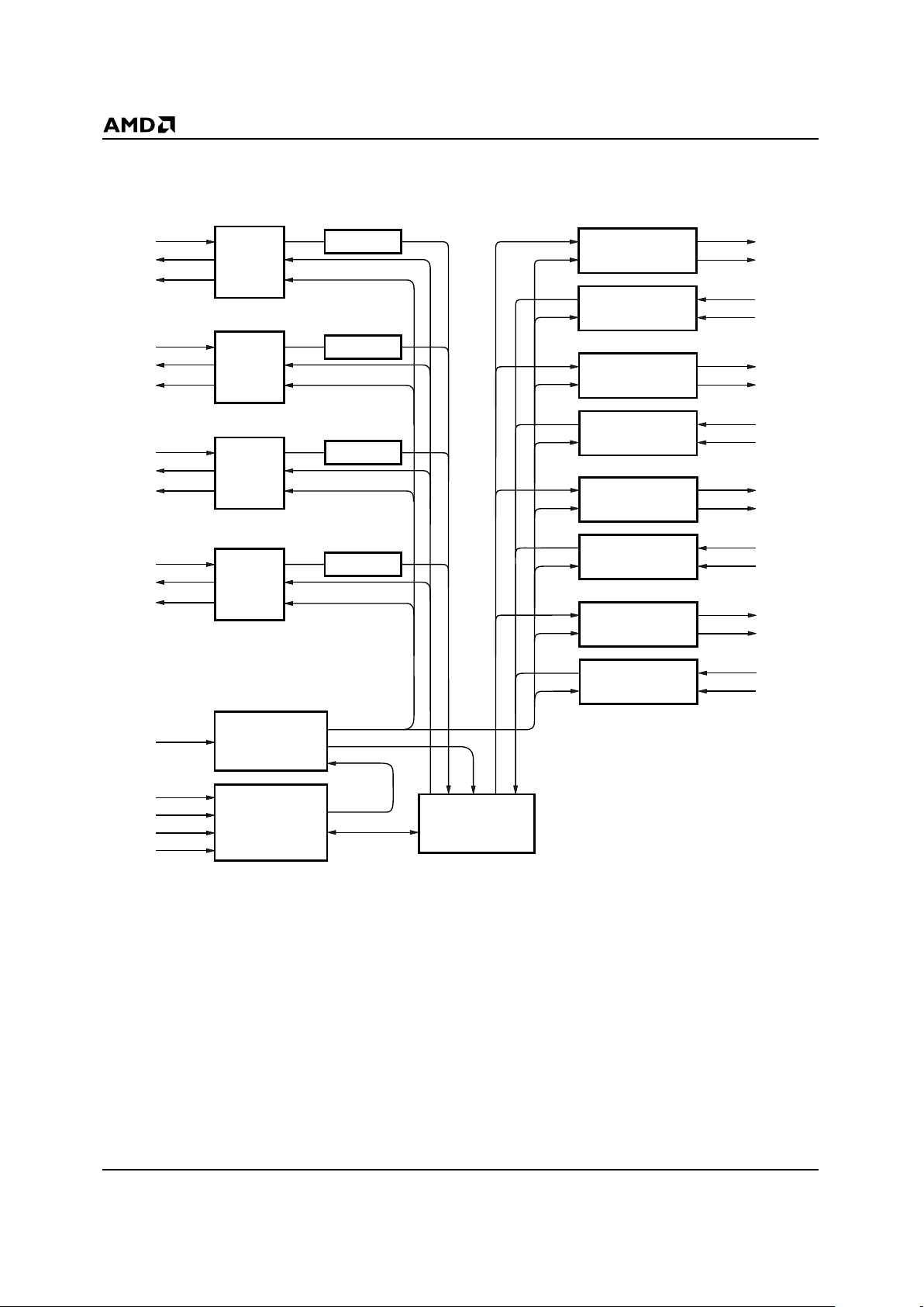
BLOCK DIAGRAM
QuIET Device
PDO[0]
PAUI Port
Line Drivers
and Receivers
PDO Squelch
Line Driver and
Wave-Shaping
TXD+
TXD-
TXD[0]+
TXD[0]-
PDI[0]
PCI[0]
PDO[1]
PAUI Port
Line Drivers
and Receivers
PDO Squelch
PDI[1]
PCI[1]
PDO[2]
PAUI Port
Line Drivers
and Receivers
PDO Squelch
PDI[2]
PCI[2]
PDO[3]
PAUI Port
Line Drivers
and Receivers
PDO Squelch
PDI[3]
PCI[3]
Internal Bias Reference
and Phase-Lock Loop
Serial Management Port
Control and Status
REXT
SDATA
DIR
CLK
RST
Collision, Loopback,
Jabber and Link Test
Line Receiver and
Smart Squelch
RXD+
RXD-
RXD[0]+
RXD[0]-
Line Driver and
Wave-Shaping
TXD+
TXD-
TXD[1]+
TXD[1]-
Line Receiver and
Smart Squelch
RXD+
RXD-
RXD[1]+
RXD[1]-
Line Driver and
Wave-Shaping
TXD+
TXD-
TXD[2]+
TXD[2]-
Line Receiver and
Smart Squelch
RXD+
RXD-
RXD[2]+
RXD[2]-
Line Driver and
Wave-Shaping
TXD+
TXD-
TXD[3]+
TXD[3]-
Line Receiver and
Smart Squelch
RXD+
RXD-
RXD[3]+
RXD[3]-
19880B-1
Page 3

Am79C988A 3
PRELIMINARY
RELATED AMD PRODUCTS
Part No.
Description
Am79C981
Integrated Multiport Repeater+ (IMR+™)
Am79C982
b
asic Integrated Multiport Repeater (
b
IMR™)
Am79C983A Integrated Multiport Repeater 2 (IMR2™)
Am79C987 Hardware Implemented Management Information Base (HIMIB™)
Am7990 Local Area Network Controller for Ethernet (LANCE)
Am7996 IEEE 802.3/Ethernet/Cheapernet Transceiver
Am79C90 CMOS Local Area Network Controller for Ethernet (C-LANCE)
Am79C98 Twisted Pair Ethernet Transceiver (TPEX)
Am79C100 Twisted Pair Ethernet Transceiver Plus (TPEX+)
Am79C900 Integrated Local Area Communications Controller (ILACC™)
Am79C940 Media Access Controller for Ethernet (MACE™)
Am79C960 PCnet™-ISA Single-Chip Ethernet Controller (for ISA bus)
Am79C961 PCnet™-ISA+ Single-Chip Ethernet Controller for ISA (with Microsoft® Plug n’ Pla y® Support)
Am79C961A PCnet™-ISA II Full Duplex Single-Chip Ethernet Controller for ISA
Am79C965 PCnet™-32 Single-Chip 32-Bit Ethernet Controller
Am79C970 PCnet™-PCI Single-Chip Ethernet Controller (for PCI bus)
Am79C970A PCnet™-PCI II Full Duplex Single-Chip Ethernet Controller (for PCI bus)
Am79C974 PCnet™-SCSI Combination Ethernet and SCSI Controller for PCI Systems
Page 4

4 Am79C988A
PRELIMINARY
CONNECTION DIAGRAM
1
44
43
42
5
4
3
2
6 41
40
7
8
9
10
11
12
13
14
15
16
17
23
24
25
26
19
20
21
22
18 27
28
39
38
37
36
35
34
33
32
31
30
29
DVSS
RST
REXT
TEST
DIR
CLK
SDATA
DVDD
TXD3+
TXD3AVSS
PDI0
PDO0
AVDD
TXD0+
TXD0-
AVSS
TXD1+
TXD1-
AVDD
TXD2+
TXD2-
RXD3-
RXD3+
AVSS
RXD2-
RXD2+
AV
DD
RXD1-
RXD1+
AVSS
RXD0-
RXD0+
PCI0
PDO1
PDI1
PCI1
PDO2
PDI2
PDO3
PDI3
PCI2
PCI3
DVSS
Am79C988A
19880B-2
Page 5

Am79C988A 5
PRELIMINARY
LOGIC DIAGRAM
LOGIC SYMBOL
Ports
PAUI
TP
TP
TP
TP
Serial
Interface
PAUI
PAUI
PAUI
19880B-3
PDO
PDI
PCI
DIR
SDATA
CLK
RST
TXD+
TXD-
RXD+
RXD-
DV
SS
AV
SS
DV
DD
AV
DD
Twisted
Pair Ports
(4 Ports)
Pseudo Attachment
Unit Interface
(PAUI) Ports
(4 Ports)
Am79C988
Serial
Management
Interface
A
19880B-4
Page 6

6 Am79C988A
PRELIMINARY
ORDERING INFORMATION
Standard Products
AMD standard products are available in se v eral packages and oper ating ranges. The order number (Valid Combination) is f ormed
by a combination of:
Valid Combinations
Valid Combinations table
list configurations planned to be
supported in volume for this device. Consult the local AMD
sales office to confirm availability of specific valid combinations and to check on newly released combinations.
Am79C988B
OPTIONAL PROCESSING
Blank = Standard processing
TEMPERATURE RANGE
C = Commercial (0˚C to +70˚C)
P A CKA GE TYPE
J = 44-pin Plastic Leaded chip carrier
(PL 044)
SPEED OPTION
Not applicable
J C
DEVICE NUMBER/DESCRIPTION
Am79C988B
Quad Integrated Ethernet
Transceiver (QuIET™)
Valid Combinations
Am79C988B JC\T
Page 7

Am79C988A 7
PRELIMINARY
PIN DESCRIPTION
Analog
PDO
0-3
Pseudo AUI Data Output
Input
Single-ended receiver . Data input from the IMR2 device .
PDI
0-3
Pseudo AUI Data Input
Output
Single-ended output driver. Data output to the
IMR2 device.
PCI
0-3
Pseudo AUI Collision Input
Output
Single-ended output driver. Collision output to the
IMR2 device.
TXD+
0-3
, TXD-
0-3
Transmit Data
Output
10BASE-T port differential drivers.
RXD+
0-3
, RXD-
0-3
Receive Data
Input
10BASE-T port differential receivers.
REXT
External Resistor
Input
REXT must be tied to AV
DD
through a 13 k Ω ± 1%
resistor.This provides the current ref erence f or all internal analog functions.
AV
DD
Analog Power
Power Pin
These pins supply +5-V power to the analog portion of
the device. These pins should be decoupled and kept
separate from the digital power plane.
AV
SS
Analog Ground
Ground Pin
These pins provide the ground reference f or the analog
portions of the QuIET circuitry.
Digital
SDATA
Serial Data
Input/Output
Transfers command and status data between the
QuIET device and the IMR2 chip.
DIR
Direction
Input
Selects the direction of command data and status data
transfer between the QuIET device and the IMR2 chip.
RST
Reset
Input, Active Low
Resets the internal registers of the QuIET device.
CLK
Clock
Input
20-Mhz clock signal. The clock signal should be the
same one that is used by all IMR2 devices connected
to the QuIET chip.
TEST
Input, Active High
Reserved for factory use only. This pin does have an
internal pull-down, but should be tied LOW for
normal operation.
DV
DD
Digital Power
Power Pin
These pins supply +5-V power to the digital portion of
the device. These pins should be decoupled and kept
separate from the analog power plane.
DV
SS
Digital Ground
Ground Pin
These pins provide the ground reference for the digital
portions of the QuIET circuitry.
Note: All digital I/O pins are CMOS and TTL compatible .
Page 8

8 Am79C988A
PRELIMINARY
FUNCTIONAL DESCRIPTION
Overview
The Am79C988A Quad Integrated Ethernet Transceiver
(QuIET
™
) device consists of four independent 10BASE-T
transceivers which are compliant with the IEEE 802.3 Section 14 (
Medium Attachment Unit for 10BASE-T Cabling
)
standard. The QuIET device includes on-chip filtering for
both transmit and receive functions, thus eliminating the
need for external filters. It provides automatic polarity
detection and correction and can operate in either normal
or full-duplex mode.
The QuIET device interfaces directly with the Pseudo
AUI (PAUI
™
) ports on the IMR2 (Am79C983A) device.
PAUI ports are functionally equivalent to the AUI interface as described in IEEE 802.3 Section 7, but are
single-ended and do not have the drive capability
specified in the standard. The QuIET device can also
be connected to standard AUI ports. Command and
status data is exchanged with the IMR2 device via a
serial management interface.
Twisted Pair Transmitters
Each TXD port is a differential twisted pair driver. When
properly terminated, TXD meets the 10BASE-T transmitter electrical requirements as specified in IEEE 802.3
Section 14.3.1.2. Proper termination, Figure 1, consists
of a single 110 ohm +
1% resistor across TXD+ and TXDand a 1:1 standard Ethernet transformer. A common
mode may be required for EMI considerations. An external capacitor is not required. The load is a twisted
pair cable that meets IEEE 802.3, Section 14.4 requirements. The cable is terminated at the other end by a
100 ohm load.
The TXD signal is filtered on the chip to reduce harmonic
content per IEEE 802.3 Section 14.3.2.1 (10BASE-T).
Since filtering is performed by the QuIET device, the
TXD signal can be connected directly to a standard
transformer. External filter modules are not required.
Figure 1. TXD Termination
Twisted Pair Receivers
Each RXD port is a differential twisted-pair receiver.
When properly terminated, RXD ports will meet the electrical requirements for 10BASE-T receivers as specified
in IEEE 802.3, Section 14.3.1.3. Proper termination is
shown in Figure 2. Each receiver has internal filtering and
does not require external filter modules.
Figure 2. RXD Termination
Receive squelch threshold voltage can be programmed
for extended distance mode. In this mode, the differential
receive threshold is reduced to allow cable lengths greater
than the 100 meters specified in the IEEE 802.3 Standard.
Polarity Detection and Reversal
The receive function includes the ability to invert the polarity of the signals appearing at the RXD+
pair if the
polarity of the received signal is reversed (such as in the
case of a wiring error). The polarity detection function is
activated following Reset or Link F ail, and will rev erse the
receive polarity based on both the polarity of any previous
Link Test Pulses and the polarity of subsequent packets
with a valid End Transmit Delimiter (ETD).
When in the Link Fail State, the QuIET de vice will recognize Link Test Pulses of either positive or negative polarity . Exit from the Link Fail state is caused by the reception
of five-to-sev en consecutive Link Test Pulses of identical
polarity . Both Link Test Pulses and packets are used to
determine the initial receive polarity . Once correct polarity
is established, the receiver subsequently accepts only
Link Test Pulses that are recognized as TRUE rather than
inverted.
The Link Test pulse follows the template of Figure
14-12 of the IEEE 802.3 10BASE-T standard.
Link Test Function
The Link Test function is implemented as specified in
the IEEE 802.3 10BASE-T standard. A Link Test pulse
is transmitted if a port has been idle for a period of more
than approximately 16 (+/-8) milliseconds (ms).
The QuIET device monitors the 10BASE-T ports for
packet and Link Pulse activity. If neither a packet nor a
Link Test pulse is receiv ed for 79 ms to 102 ms, the port
will enter the Link Test Fail State and the QuIET de vice
will inhibit the transmit and receive functions for that
port. Link pulses are transmitted when idle conditions
are met. When a packet or five-to-seven consecutive
Link Test pulses is received, the port exits the Link Fail
State and transmit/receive functions are restored.
19880B-5
TXD+
TXD-
110 Ω
1:1
Twisted Pair
100 Ω
RXD+
RXD-
1:1
Twisted Pair
100 Ω
100 Ω
19880B-6
Page 9

Am79C988A 9
PRELIMINARY
PAUI Ports
The PAUI ports are functionally equivalent to AUI ports
as described in IEEE 802.3, Section 7. However, they
are single ended and, therefore, are not an e xact match
with the electrical specifications.
PDO, PDI, and PCI are functionally similar to DO, DI,
and CI, respectively. PDO is the PAUI input from the
IMR2 device. This signal is transmitted by the corresponding TXD port. PDI is the data output to the IMR2
device and is the data received by the corresponding
RXD port. PDI also loops back data received by PDO
to the IMR2 device. PCI is the collision output to the
IMR2 device and indicates either a collision on the corresponding port or an excessive continuous data stream
on the corresponding PDO. PCI sends a 10-MHz square
wave during collision and jabber.
Collision Handling
Collision is defined for the QuIET device as data being
simultaneously transmitted and received at the corresponding TXD and RXD pins. When a collision is detected, the QuIET device sends a 10 MHz signal over
the corresponding PCI pin. This is the only action tak en
by the QuIET device. The generation of the JAM signal
is performed by the IMR2 device.
Jabber Protection
The Jabber function inhibits the twisted pair transmit
function of the port if the PDO circuit is active for an
excessive period (> 30 ms). If the maximum transmit
time is exceeded, the transmitter circuitry is disabled,
PDO to PDI loopback is disabled, and a 10 MHz signal
is transmitted by PCI. Once the data stream is remov ed
from PDO, 350 ms will elapse before PCI stops transmitting the 10 MHz signal and the TXD circuitry is enabled again. Note that a properly functioning repeater
device will never jabber because of the MAU Jabber
Lockup Protection (MJLP).
Transceiver Modes
The QuIET transceivers have two modes of operation:
Normal and Full Duplex. In Normal mode, the data flows
only in one direction at a time. In Full-Duplex mode , the
collision circuitry and the loopback circuitry are disabled. Therefore, transmit and receive can occur simultaneously . The transceiv er mode is selected through the
serial management interface, which is explained further
in the
Management Commands
and
Transceiver Mode
Selection
sections.
Normal Mode
The QuIET device defaults to the Normal mode at power
up and reset. In this mode, no twisted pair port can
transmit and receive data simultaneously. If a port receives data when it is transmitting, the QuIET device
sends a collision signal to the IMR2 device via the corresponding PCI pin.
Note: The IMR2 device only supports Normal operation.
Full-Duplex Mode
In Full-Duplex mode a port can transmit and receive simultaneously , and Collision and P A UI Loopback functions are
disabled. The normal loopback of PDO to PDI is disabled
to allow the RXD signal to be transmitted on PDI.
PCI is disabled and Jabber status is only available to
the controller through the serial management interface.
The serial management interface also transmits Jabber
status when the QuIET device is in Normal mode.
Serial Management Interface
Command and status data are transferred between the
QuIET device and the IMR2 device via SDATA. (See
Figure 4 for proper interconnections.) The direction of
SDATA is set by DIR. All activity on SDATA starts at the
edge (rising or falling) of DIR.
The DIR pin of the QuIET device connects to DIR[1] of
the IMR2 device. The IMR2 device continually cycles
DIR[1] LOW and HIGH. LOW is status reporting (SDA TA
Write) and HIGH is management commands (SDATA
Read). The controller (IMR2 device) should keep DIR
at one level for the entire bit stream. The status bit
stream is described in the
Status Reporting
section,
and
the command bit stream is described in the
Manage-
ment Commands
section
.
Each bit on SDAT A is held f or
2-bit times (200 ns).
Status Reporting
When DIR switches from HIGH to LOW, the QuIET device drives SDATA with status information (left to right)
in the format shown below . After the 29th bit, the SDAT A
driver turns off. The SDATA driver also turns off if DIR
switches HIGH before the 29th bit.
Status Information Format
01010A0A1A2A3B0B1B2B3C0C1C2C3D0D1D2D3SSSSSSSS
Preamble
The 01010 preamble is an indication to the IMR2 that
the transceiver is a QuIET device.
QuIET Device ID
A0A1A2A
3
The QuIET device returns 0000.
01010 Preamble
A
n
QuIET device ID (0000 for QuIET device)
B
n
0 Link Fail
1 Link Pass
C
n
0 Received Polarity Reversed
1 Received Polarity Correct
D
n
0 No Jabber
1 Jabber
S Not used, logic HIGH
Page 10

10 Am79C988A
PRELIMINARY
Link Status
B0B1B2B
3
The QuIET device reports the Link Status of each port.
If Link T est is disab led, Link Status indicates a Link Pass.
B
n
0 Link Fail
1 Link Pass
Receive Polarity Status
C0C1C2C
3
The QuIET device reports the polarity status of each port.
C
n
0 Reversed Polarity
1 True Polarity
Jabber Condition
D0D1D2D
3
The QuIET device reports the Jabber Condition status
for each port. Jabber is defined as continuous transmissions by a port for more than 30 ms.
D
n
0 No Jabber
1 Jabber
Management Commands
When DIR switches from LOW to HIGH, the QuIET device reads the command sequence over SDATA. Each
management command character is held for 2-bit times
(200 ns). The command format is as follows.
Management Command Format
0E0E1E2E3F0F1F2F3G0G1G2G3H0H1H2H3I J0J1J2J3KSSSSSSS
Note: The QuIET device requires DIR to be high for a
minimum of 29 data bits (one bit is four MCLKs), which
automatically occurs with the IMR2 device. If any other
type of controller is used, DIR must still be high at least
29-bit times. After I, SDATA can be all ones.
Extended Distance Option
E0E1E2E
3
This command modifies the RXD circuit of the transceiver to accommodate signal-attenuation lines longer
than 100 meters.
E
n
0 Disable Extended Distance Option
1 Enable Extended Distance Option
Link Test Enable
F0F1F2F
3
This command enables the corresponding port to perform a Link Test. Link Status will report Link Pass if the
Link Test is disabled.
F
n
0 Disable Link Test
1 Enable Link Test
Transmit Link Pulse Enable
G0G1G2G
3
This command enables the corresponding port to transmit a Link Pulse. The pulse will be transmitted if either
a packet or a pulse has not been transmitted f or 16 ms.
Note that Link Pulses are transmitted when ports are in
Link Test Fail.
G
n
0 Disable Link Pulse Transmit
1 Enable Link Pulse Transmit
Auto Polarity Correction Enable
H0H1H2H
3
This command allows the QuIET device to detect and
correct the polarity of signals at RXD.
H
n
0 Enable Auto Polarity
1 Disable Auto Polarity
Loopback Test Enable
This command enables or disables the loopback test
for the twisted pair ports. When enabled, the signal on
RXD is retransmitted on TXD. The default condition is
loopback test disabled. Note that the TXD drivers hav e
on-chip filtering, which may cause the TXD output to
be different from the corresponding RXD input during
this test.
I 0 Enable Loopback Test
1 Disable Loopback Test
Transceiver Mode Selection
J0J1J2J
3
This command sets the QuIET device either in Full-Duplex or Normal mode. The default is Normal mode.
J
n
0 Full Duplex
1 Normal
E
n
Extended Distance 0 Disabled
1 Enabled
F
n
Link Test 0 Disabled
1 Enabled
G
n
Transmit Link Test Pulses 0 Disabled
1 Enabled
H
n
Enable Polarity Correction
0 Enabled
1 Disabled
I Loopback Test (All Ports) 0 Enabled
1 Disabled
J
n
Transceiver Mode 0 Full Duplex
1 Normal (Default
condition - IMR2 only
supports Normal)
K CMOS/PAUI Mode 0 CMOS Mode
1 PAUI Mode
S Not used Logic HIGH
Page 11

Am79C988A 11
PRELIMINARY
CMOS/PAUI Mode Selection
This command sets the QuIET interface drivers (PDO,
PDI, PCI) to be driven at normal PAUI signal levels or
CMOS voltage levels. The default is PAUI levels. Refer
to the DC Characteristics table for voltage levels.
K 0 CMOS Levels
1 PAUI Levels
Reset Function
The QuIET device enters the reset state when the reset
pin (RST) is held LOW. All ports, status registers, and
command registers are put into their default state. When
powering up the device, the RST
pin should be held
LOW for 150 microseconds (µs). At other times, the RST
pin should be held LOW for a minimum of 4 µs. The
default conditions are detailed below.
Command and Status Default Conditions
Command Default
Extended Distance Disabled
Link Test Enabled
Link Pulse Transmit Enabled
Correct Polarity Disabled
Loopback Test Disabled
Transceiver Mode Selection Normal
CMOS/PAUI Mode PAUI Mode
Status Default
Device
QuIET
Link
Fail
Polarity
Correct
Jabber
No Error
Page 12

12 Am79C988A
PRELIMINARY
SYSTEMS APPLICATIONS
10BASE-T Repeaters
The IMR2/QuIET chipset provides a system solution to
designing 10BASE-T repeaters. Figure 3 shows the
necessary connections between the IMR2 device and
the QuIET device. Although only one QuIET device is
shown for clarity, three QuIET devices are required to
build a 12-port 10BASE-T repeater.
Port Switching
The IMR2/QuIET chipset supports port switching, which
is the ability to move individual ports to any one of multiple Ethernet backplanes under software control. To implement port switching, each port on the QuIET device
is connected to two or more IMR2 devices in parallel.
Each IMR2 device defines a different logical repeater
and constitutes a separate Ethernet collision domain.
For each port on the QuIET device, only one corresponding port on the IMR2 devices is enabled at any
one time.
Figure 4 shows the IMR2 device-to-QuIET device connections necessary for port switching. Note that only
one QuIET device is shown f or clarity. A full implementation would use three QuIET devices to provide 12
10BASE-T ports that can be individually switched between three Ethernet collision domains.
The IMR2 and QuIET devices must share a common
ground plane and a common power plane. Failure to
meet this design requirement may result in false assertion of internal carrier sense or inability to unsquelch in
either PDI (for IMR2) or PDO (for QuIET).
Connection to Standard AUI Port
The PAUI ports on the QuIET device can also be connected to standard AUI ports when used with devices
other than the IMR2 chip. Connection to a standard A UI
port is not meant to support a full length AUI cable . The
AUI connection should remain on the same board as
shown in Figure 6.
Connection to CMOS Circuits
The PAUI ports on the QuIET device can also drive
CMOS loads for other devices , including switches. The
PDO, PDI, and PCI signals connect directly to the
CMOS device. Note that CMOS mode must be
selected in the Management Command Frame.
Page 13

Am79C988A 13
PRELIMINARY
Figure 3. IMR2 Device to QuIET Device Connection
QuIET
Typical
IMR2
TP Connector
TP Connector
TP Connector
TP Connector
100 Ω
110 Ω
100 Ω
110 Ω
100 Ω
100 Ω
13K Ω
110 Ω
110 Ω
TXD0+
TXD0-
RXD0+
RXD0-
TXD1-
RXD1+
RXD1-
TXD2+
TXD2-
RXD2+
RXD2-
TXD3+
TXD3-
RXD3+
RXD3-
TXD1+
REXT
RST
CLK
PDO0
PDI0
PCI0
PDO0
PDI0
PCI0
PDO1
PDI1
PCI1
PDO1
PDI1
PCI1
PDO2
PDI2
PCI2
PDO2
PDI2
PCI2
PDO3
PDI3
PCI3
PDO3
PDI3
PCI3
AV
DD
MCLK
RST
19880B-7
Note: Common mode chokes may be required.
Page 14

14 Am79C988A
PRELIMINARY
Figure 4. IMR2 Device To QuIET Device Serial Interface
Figure 5. Port Switching
SDATA[3]
SDATA[2]
SDATA[1]
SDATA[0]
DIR[1]
DIR[0]
IMR2 Device
QuIET Device 2
MCLK
RST
SDATA
DIR
CLK
QuIET Device 1
RST
QuIET Device 0
Reset
CLK
SDATA
DIR
CLK
RST
SDATA
DIR
CLK
RST
NC
NC
19880B-8
A
m
7
9
C
9
8
8
Backplane 0
Am79C983
IMR2 0
Backplane 1
Am79C983
IMR2 1
Am79C983
IMR2 2
Backplane 2
PDO
PDI
PCI
PDO
PDI
PCI
PDO
PDI
PCI
PDO
PDI
PCI
SDATA[0]
DIR[1]
PDO
PDI
PCI
PDO
PDI
PCI
PDO
PDI
PCI
PDO
PDI
PCI
SDATA
DIR
TX
RX
TX
RX
TX
RX
TX
RX
Port 0
Port 1
Port 2
Port 3
PDO
PDI
PCI
PDO
PDI
PCI
PDO
PDI
PCI
PDO
PDI
PCI
PDO
PDI
PCI
PDO
PDI
PCI
PDO
PDI
PCI
PDO
PDI
PCI
19880B-9
Page 15

Am79C988A 15
PRELIMINARY
Figure 6. AUI to PAUI Connections
1:1
0.1 µF
PDO
DO+
DO-
1:1
0.1 µF
PDI
DI+
DI-
1:1
CI+
CI-
78 Ω
200 Ω
200 Ω
10 KΩ
12 KΩ
10 KΩ
AUI
Port
QuIET
Device
0.1 µF
PCI
10 KΩ
10 KΩ
19880B-10
Page 16

16 Am79C988A
PRELIMINARY
ABSOLUTE MAXIMUM RATINGS
Storage Temperature. . . . . . . . . . . . . –65°C to +150°C
Ambient Temperature Under Bias. . . . . . . . . 0 to 70°C
Supply Voltage referenced to
AVSS or DVSS (AVDD, DVDD) . . . . . . . . . . . . . .–0.3 to +6V
Stresses above those listed under ABSOLUTE MAXIMUM
RATINGS may cause permanent device failure. Functionality
at or above these limits is not implied. Exposure to Absolute
Maximum Ratings for extended periods may affect device reliability. Programming conditions may differ.
OPERATING RANGES
Commercial (C) Devices
Temperature (TA) . . . . . . . . . . . . . . . . . .0°C to + 70° C
Supply Voltages (VDD). . . . . . . . . . . . . . . . . +5 V ±5%
Operating ranges define those limits between which the
functionality of the device is guaranteed.
DC CHARACTERISTICS over operating ranges unless otherwise specified
Parameter
Symbol
Parameter Description
Test Conditions
Min
Max
Unit
Digital I/O
V
IL
Input LOW Voltage DVSS = 0.0 V -0.5 0.8 V
V
IH
Input HIGH Voltage 2.0 DVDD +0.5 V
V
OL
Output LOW Voltage IOL=4.0 mA - 0.4 V
V
OH
Output HIGH Voltage IOH =-0.4 mA 2.4 - V
I
IH
Input Leakage Current HIGH (DIR,
SDATA, CLK, RST
)
0<VIN<DV
DD
- 10 µA
I
IL
Input Leakage Current LOW (DIR,
SDATA, CLK, TEST)
0V<VIN<DV
DD
- -10 µA
I
ILDH
Input Leakage Current HIGH (TEST) 0<VIN<DV
DD
- 500 µA
I
ILDL
Input Leakage Current LOW (RST) 0V<VIN<DV
DD
- -500 µA
PAUI Ports
V
POH
Output HIGH Voltage PAUI Mode V
DD/2
+ 0.45 - V
V
POL
Output LOW Voltage PAUI Mode - V
DD/2
- 0.45 V
V
PIH
Input HIGH Voltage PAUI Mode V
DD/2
+ 0.45 - V
V
PIL
Input LOW Voltage PAUI Mode - V
DD/2
- 0.45 V
I
PILH
Input Leakage Current HIGH AVDD = MAX - 10 µA
I
PILL
Input Leakage Current LOW AVDD = MAX - -10 µA
V
PASQ
PDO Squelch (the value PDO must go to
before internal PDO carrier sense can be
turned on)
V
DD/2
- 0.400 V
DD/2
- 0.175 mV
Twisted Pair Ports
I
IRXD
Input Current at RXD± AVSS<VIN<AV
DD
-500 500 µA
R
RXD
RXD Differential Input Resistance (Note 1) 10 - kΩ
V
TIVB
RXD±, Open Circuit Input Voltage
(Bias)
IIN = 0 mA AVDD-3.0 AVDD-1.5 V
V
TIDV
Differential Mode Input Voltage Range
(RXD)
AVDD = 5.0 V -3.1 3.1 V
V
TSQ+
RXD Positive Squelch Threshold
(Peak)
Sinusoid 5 MHz <f< 10 MHz 300 520 mV
V
TSQ-
RXD Negative Squelch Threshold
(Peak)
Sinusoid 5 MHz <f< 10 MHz -520 -300 mV
V
THS+
RXD Post-Squelch Positive Threshold
(Peak)
Sinusoid 5 MHz <f< 10 MHz 120 293 mV
V
THS-
RXD Post-Squelch Negative Threshold
(Peak)
Sinusoid 5 MHz <f< 10 MHz -293 -120 mV
Page 17

Am79C988A 17
PRELIMINARY
Note:
1. CMOS Mode on PAUI signals is guaranteed by design and is compatible with normal CMOS levels present on other QuIET
device pins.
V
LTSQ+
RXD Positive Squelch Threshold Extended Distance Mode
Sinusoid 5 MHz <f< 10 MHz 180 312 mV
V
LTSQ-
RXD Positive Squelch Threshold Extended Distance Mode
Sinusoid 5 MHz <f< 10 MHz -312 -180 mV
V
LTHS+
RXD Post-Squelch Positive Threshold
Extended Distance Mode
Sinusoid 5 MHz <f< 10 MHz 80 175 mV
V
LTHS-
RXD Post-Squelch Negative Threshold
Extended Distance Mode
Sinusoid 5 MHz <f< 10 MHz -175 -80 mV
V
RXDTH
RXD Switching Threshold (Note 1) -60 +60 mV
V
TXI
TXD± Differential Output Voltage Imbalance
-40 +40 mV
I
TXOFF
TXD± Idle Output Current DV
DD
= 5V
(Note 2)
-2 2 µA
Power Supply Current
I
DDTX
Power Supply Current (All 4 ports Transmitting Including TXD current)
F = 20 MHz VDD = V
MAX
(Uses Twisted Pair Switching
Test Current)
- 380 mA
I
DDI
Power Supply Current Idle F= 20 MHz VDD =V
MAX
- 120 mA
Parameter
Symbol
Parameter Description
Test Conditions
Min
Max
Unit
Page 18

18 Am79C988A
PRELIMINARY
SWITCHING CHARACTERISTICS over operating ranges unless otherwise specified
Parameter
Symbol
Parameter Description
Test Conditions
Min
Max
Unit
Clock and Reset Timing
t
CLK
CLK Clock Period (Note 1) 49.995 50.005 ns
t
CLKH
CLK Clock High 20 30 ns
t
CLKL
CLK Clock Low 20 30 ns
t
CLKR
CLK Rise Time (Note 1) - 10 ns
t
CLKF
CLK Fall Time (Note 1) - 10 ns
t
RST
Reset Pulse Width (RST pin LOW) 4 - µs
t
PRST
Reset Pulse Width at Power Up 150 - µs
Transmit Timing
t
PWODO
PDO Pulse Width Accept/ Reject Threshold
Input > V
ASQ
(Max)
(Note 3)
15 35 ns
t
PWKDO
PDO Pulse Width Maintain/Turn-Off
Threshold
Input > V
ASQ
(Max)
(Note 4)
110 200 ns
t
TON
Transmit Start-Up Delay - 300 ns
t
TSD
Transmit Static Propagation Delay (PDO
to TXD)
- 200 ns
t
TETD
Transmit End of Transmission (for TXD) 250 450 ns
t
PERLP
Idle Signal Period (Note 7) 8 24 ms
t
PWLP
Link Pulse Width (Note 1) 75 120 ns
t
JA
Transmit Jabber Activation Time (Note 7) 20 150 ms
t
JR
Transmit Jabber Reset Time (Note 7) 250 750 ms
t
JREC
Transmit Jabber Recovery Time (Minimum time gap between packets to prevent
Jabber activation)
(Note 1) 1.0 - µs
t
DODION
PDO to PDI Start-up Delay 300 ns
t
DODISD
PDO to PDI Static Propagation Delay - 100 ns
Receive Timing
t
PWORD
RXD Pulse Width Accept/Reject
Threshold
(Note 5) 5 35 ns
t
PWKRD
RXD Pulse Width Maintain/Turn-Off
Threshold
(Note 6) 136 200 ns
t
RON
Receiver Start-up Delay (RXD to PDI) 200 400 ns
t
RVD
First Validly Timed Bits - t
RON
+100 ns
t
RSD
Receiver Static Propagation Delay (RXD
to PDI)
- 70 ns
t
RETD
PDI End of Transmission 200 - ns
t
RR
PDI, PCI Rise Time (Note 1) - 10 ns
t
RF
PDI, PCI Fall Time (Note 1) - 10 ns
t
RM
PDI, PCI Rise and Fall Time Mismatch (tRR
- t
RF
)
(Note 1) - 5 ns
Collision Timing
t
CON
Collision Turn On Delay - 500 ns
t
COFF
Collision Turn Off Delay - 500 ns
t
CPER
Collision Period (Note 1) 87 117 ns
t
CPW
Collision Output Pulse Width (Note 1) 40 60 ns
Serial Interface Timing
t
SDSU
CLK to DIR Setup Time (Note 7) 10 - ns
t
SDHD
DIR Hold Time (Note 7) 10 - ns
t
SSSU
CLK to SDATA Setup Time (Note 7) 10 - ns
t
SSHD
CLK to SDATA Hold Time (Note 7) 10 - ns
t
SSDO
CLK to Output Delay - 40 ns
Page 19

Am79C988A 19
PRELIMINARY
Notes:
1. Parameter is not tested.
2. Uses switching test load.
3. PDO pulses narrower than
t
PWODO
(min) will be rejected; PDO pulses wider than
t
PWODO
(max) will turn internal PDO carrier
sense on.
4. PDO pulses narrower than
t
PWKDO
(min) will maintain internal PDO carrier sense on; PDO pulses longer than
t
PWKDO
(max)
will turn internal PDO carrier sense off.
5. RXD pulses narrower than
t
PWORD
(min) will be rejected; RXD pulses longer than
t
PWORD
(max) will turn internal RXD carrier
sense on.
6. RXD pulses narrower than
t
PWKRD
(min) will maintain internal RXD carrier sense; RXD pulses longer than
t
PWKRD
(max) will
turn internal RXD carrier sense off.
7. Parameter tested functionally.
t
SSDOZ
Clock to High Impedance Output - 40 ns
t
SDS
DIR going HIGH to SDATA Input Valid (Note 7) -50 100 ns
t
DDS
DIR going LOW to SDATA Output Valid (Note 7) 100 150 ns
Parameter
Symbol
Parameter Description
Test Conditions
Min
Max
Unit
Page 20

20 Am79C988A
PRELIMINARY
KEY TO SWITCHING WAVEFORMS
SWITCHING WAVEFORMS
Figure 7. Clock (CLK) Timing
Figure 8. Reset Pulse
KS00010
Must be
Steady
May
Change
from H to L
May
Change
from L to H
Does Not
Apply
Don’t Care,
Any Change
Permitted
Will be
Steady
Will be
Changing
from H to L
Will be
Changing
from L to H
Changing,
State
Unknown
Center
Line is HighImpedance
“Off” State
WAVEFORM INPUTS OUTPUTS
tCLK
tCLKH
tCLKL
tCLKF
tCLKR
19880B-11
tRST
tPRST
RST
19880B-12
Page 21

Am79C988A 21
PRELIMINARY
SWITCHING WAVEFORMS
Figure 9. Transmit Signals
Figure 10. Receive Signals
Figure 11. Collision Signals
tTON
TXD+
PDI
tDODION
tTETD
tTSD
tPWKDO
tPWODO
tPWKDO
tTSD
tTSD
PDO
TXD-
tDODISD
19880B-13
19880B-14
VTHS+
VTHS-
tPWKRD
tPWORD
RXD
PDI
tRON
tPWKRD
tRSD
tRF
tRR
tRETD
tCPW
tCPER
tCON
tCOFF
PDO
RXD
PCI
19880B-15
Page 22

22 Am79C988A
PRELIMINARY
SWITCHING WAVEFORMS
Figure 12. Transmit Link Beat Pulse
Figure 13. Jabber Function
tPWLP
tPERLP
19880B-16
tJR
0V
0V
0V
50%
50%
PDO
TXD
PCI
tJA
19880B-17
Page 23

Am79C988A 23
PRELIMINARY
SWITCHING WAVEFORMS
Figure 14. Serial Interface Waveforms
Figure 15. Serial Interface SDATA Transmit and Start Receive
CLK
DIR
SDATA
DIR
SDATA
DIR
SDATA
DIR
SDATA
tSDSU
tSSSU
tSSHD
tSDHD
tSSDO
tSSDO
M2
M3
L3
L2
E1
{
{
{
{
-0
-1
19880B-18
DIR
SDATA
TSDS
TDDS
(min)
(max)
TDDS
19880B-19
Page 24

24 Am79C988A
PRELIMINARY
SWITCHING TEST CIRCUITS
Figure 16. Switching Test Circuit
Figure 17. Twisted Pair Switching Test Circuit
VDD
VSS
Test Pin
Test Point
100pF
R
330*
R = 330 for PAUI
1kΩ for SDATA
*Not used for SDATA
19880B-20
TXD+ TP
TPTXD-
110 Ω
19880B-21
Page 25

Am79C988A 25
PRELIMINARY
PHYSICAL DIMENSIONS*
PL 044
44-Pin Plastic Leaded Chip Carrier (Measured in inches)
REVISION SUMMARY
This revision (B) reflects changes to Figures 3, 6, and
17. Changes have also been made to the Ordering In-
formation page, and the DC Characteristics and Switching Characteristics tables. No other technical changes
have been made.
Trademarks
Copyright © 1997 Advanced Micro Devices, Inc. All rights reserved.
AMD, the AMD logo, and combinations thereof, and QuIET, IMR2, and PAUI are trademarks of Advanced Micro Devices, Inc.
Product names used in this publication are for identification purposes only and may be trademarks of their respective companies.
TOP VIEW
SEATING PLANE
.685
.695
.650
.656
Pin 1 I.D.
.685
.695
.650
.656
.026
.032
.050 REF
.042
.056
.062
.083
.013
.021
.590
.630
.500
REF
.009
.015
.165
.180
.090
.120
16-038-SQ
PL 044
EC80
11.3.97 lv
SIDE VIEW
 Loading...