

Page 1

PRELIMINARY
Am79C985
enhanced Integrated Multiport Repeater Plus (eIMR+™)
DISTINCTIVE CHARACTERISTICS
■
Repeater functions compliant with IEEE 802.3
Repeater Unit specifications
■
Direct interface with the Am79C987 Hardware
Implemented Management Information Base
(HIMIB™) device for building a basic managed
multiport repeater
■
Full software backwards compatibility with
existing hub designs using Integrated Multiport
Repeater Plus (IMR+™)/HIMIB devices
■
Network management and optional feature
accessibility through a dedicated serial
management port
■
Four integral 10BASE-T transceivers with onchip filtering eliminating the need for external
filter modules on the 10BASE-T transmit-data
(TXD) and receive-data (RXD) lines
■
One Reversible Attachment Unit Interface
(RAUI™) port used either as a standard IEEEcompliant AUI port for connection to a Medium
Attachment Unit (MAU) or a reversed port for
direct connection to a Media Access Controller
(MAC)
■
Low cost suitable for managed multiport
repeater designs
■
Number of repeater ports easily expandable
with support for up to seven eIMR+ devices
without the need for an external arbiter
■
All ports capable of being individually isolated
(partitioned) in response to excessive collision
conditions or fault conditions
■
Flexible LED support for individual port status
and network utilization LEDs
■
Programmable extended distance mode on RXD
lines allowing connection to cables longer than
100 meters
■
Link Test function and Link Test pulse
transmission capable of being disabled through
the management port allowing devices that do
not implement the Link Test function to work
with the eIMR+ device
■
Programmable automatic polarity detection and
correction option permitting automatic
recovery from wiring errors
■
Full amplitude and timing regeneration for
retransmitted waveforms
■
CMOS device with a single +5-V supply
GENERAL DESCRIPTION
The enhanced Integrated Multiport Repeater Plus
(eIMR+) device is a VLSI integrated circuit that provides a system-level solution to designing managed
multiport repeaters. The device integrates the repeater
functions specified in Section 9 of the IEEE 802.3
standard and Twisted Pair Transceiver functions complying with the 10BASE-T standard.
The eIMR+ device provides f our Twisted Pair (TP) ports
and one reversible AUI (RAUI) port for direct connection to a MAC. The total number of ports per repeater
unit can be increased by connecting multiple eIMR+
devices through their expansion ports, hence, minimizing the total cost per repeater port.
This document contains information on a product under development at Advanced Micro Devices. The information
is intended to help you evaluate this product. AMD reserves the right to change or discontinue work on this proposed
product without notice.
The eIMR+ device also provides a connection to the
Am79C987 HIMIB device. The HIMIB device monitors
all the necessary counters, attributes, actions, and
notifications specified by IEEE 802.3, Section 19
(Layer Management f or 10 Megabit per second (Mbps)
Baseband Repeaters). When the eIMR+ and HIMIB
devices are used together as a chip set, they provide a
cost-effective solution to the problem of designing
10BASE-T basic managed multiport repeaters.
The device is fabricated in CMOS technology and
requires a single +5-V supply.
Publication# 20651 Rev: B Amendment/0
Issue Date: January 1998
Page 2

BLOCK DIAGRAM
TX
MUX
Preamble
PRELIMINARY
Jam Sequence
SELI[1:0]
ACK
SELO
COL
Expansion Port
DAT
JAM
LDA[4:0], LDB[4:0]
STR
LDGA, LDGB
LDC[2:0]
ACT[7:0]
LED
Interface
SI
SI_D
Test
SO
SCLK
AMODE
CRS_I
and
Port
Management
CRS
FIFO
Decoder
Manchester
RX
RX
AUI
Port
DI±
CI±
MUX
MUX
DO±
Lock
Phase
FIFO
CONTROL
Loop
TP
RXD±
0
Port
TXD±
Encoder
Manchester
Control
eIMR+ Chip
3
TP
Port
TXD±
RXD±
Link T est
Partitioning
Reset
RST
Clock
Gen
CLK
Timers
20651B-1
.
2 Am79C985
Page 3
PRELIMINARY
ORDERING INFORMATION
Standard Products
AMD standard products are available in se v eral packages and oper ating ranges. The order number (Valid Combination) is f ormed
by a combination of the elements below.
Am79C985
J
\W
C
ALTERNATE PACKAGING OPTION
\W = Trimmed and formed in a tray
TEMPERATURE RANGE
C = Commercial (0˚C to +70˚C)
P ACKA GE TYPE
J = 84-Pin Plastic Leaded Chip Carrier (PL 084)
K = 100-Pin Plastic Quad Flat Pack (PQR100)
SPEED OPTION
Not Applicable
Valid Combinations
Am79C985 JC, KC\W
DEVICE NUMBER/DESCRIPTION
Am79C985
enhanced Integrated Multiport Repeater Plus (eIMR+)
Valid Combinations
Valid Combinations list configurations planned to be supported in volume for this device. Consult the local AMD sales
office to confirm availability of specific valid combinations and
to check on newly released combinations.
Am79C985 3
Page 4

RELATED PRODUCTS
PRELIMINARY
Part No.
Am7990
Am7992B Serial Interface Adapter (SIA)
Am7996 IEEE 802.3/Ethernet/Cheapernet Transceiver
Am79C90 CMOS Local Area Network Controller for Ethernet (C-LANCE)
Am79C98 Twisted Pair Ethernet Transceiver (TPEX)
Am79C100 Twisted Pair Ethernet Transceiver Plus (TPEX+)
Am79C981 Integrated Multiport Repeater Plus (IMR+™)
Am79C982 basic Integrated Multiport Repeater (bIMR™)
Am79C983 Integrated Multiport Repeater 2 (IMR2™)
Am79C984A enhanced Integrated Multiport Repeater (eIMR™)
Am79C987 Hardware Implemented Management Information Base (HIMIB™)
Am79C988 Quad Integrated Ethernet Transceiver (QuIET™)
Am79C900 Integrated Local Area Communications Controller (ILACC™)
Am79C940 Media Access Controller for Ethernet (MACE™)
Am79C960 PCnet™-ISA Single-Chip Ethernet Controller (for ISA bus)
Am79C961 PCnet™-ISA+ Single-Chip Ethernet Controller for ISA (with Microsoft® Plug n’ Play® Support)
Am79C961A PCnet™-ISA II Full Duplex Single-Chip Ethernet Controller for ISA
Am79C965 PCnet™-32 Single-Chip 32-Bit Ethernet Controller
Am79C970 PCnet™-PCI Single-Chip Ethernet Controller (for PCI bus)
Am79C970A PCnet™-PCI II Full Duplex Single-Chip Ethernet Controller (for PCI bus)
Am79C974 PCnet™-SCSI Combination Ethernet and SCSI Controller for PCI Systems
Local Area Network Controller for Ethernet (LANCE)
Description
.
4 Am79C985
Page 5

TABLE OF CONTENTS
DISTINCTIVE CHARACTERISTICS . . . . . . . . . . . . . . . . . . . . . . . . . . . . . . . . . . . . . . . . . . . . . . . . 1
GENERAL DESCRIPTION . . . . . . . . . . . . . . . . . . . . . . . . . . . . . . . . . . . . . . . . . . . . . . . . . . . . . . .2
BLOCK DIAGRAM . . . . . . . . . . . . . . . . . . . . . . . . . . . . . . . . . . . . . . . . . . . . . . . . . . . . . . . . . . . . . 3
ORDERING INFORMATION . . . . . . . . . . . . . . . . . . . . . . . . . . . . . . . . . . . . . . . . . . . . . . . . . . . . . .4
Standard Products . . . . . . . . . . . . . . . . . . . . . . . . . . . . . . . . . . . . . . . . . . . . . . . . . . . . . . . . . . 4
RELATED PRODUCTS . . . . . . . . . . . . . . . . . . . . . . . . . . . . . . . . . . . . . . . . . . . . . . . . . . . . . . . . .5
CONNECTION DIAGRAMS (PL 084) . . . . . . . . . . . . . . . . . . . . . . . . . . . . . . . . . . . . . . . . . . . . . . .8
CONNECTION DIAGRAMS (PQR100) . . . . . . . . . . . . . . . . . . . . . . . . . . . . . . . . . . . . . . . . . . . . . .9
LOGIC SYMBOL . . . . . . . . . . . . . . . . . . . . . . . . . . . . . . . . . . . . . . . . . . . . . . . . . . . . . . . . . . . . . .10
LOGIC DIAGRAM . . . . . . . . . . . . . . . . . . . . . . . . . . . . . . . . . . . . . . . . . . . . . . . . . . . . . . . . . . . . . 10
PIN DESIGNATIONS (PL084) . . . . . . . . . . . . . . . . . . . . . . . . . . . . . . . . . . . . . . . . . . . . . . . . . . . 11
Listed by Pin Number. . . . . . . . . . . . . . . . . . . . . . . . . . . . . . . . . . . . . . . . . . . . . . . . . . . . . . . 11
PIN DESIGNATIONS (PQR100) . . . . . . . . . . . . . . . . . . . . . . . . . . . . . . . . . . . . . . . . . . . . . . . . . . 12
Listed by Pin Number. . . . . . . . . . . . . . . . . . . . . . . . . . . . . . . . . . . . . . . . . . . . . . . . . . . . . . . 12
PIN DESCRIPTION . . . . . . . . . . . . . . . . . . . . . . . . . . . . . . . . . . . . . . . . . . . . . . . . . . . . . . . . . . . 13
AUI Port . . . . . . . . . . . . . . . . . . . . . . . . . . . . . . . . . . . . . . . . . . . . . . . . . . . . . . . . . . . . . . . . . . 13
Twisted Pair Ports . . . . . . . . . . . . . . . . . . . . . . . . . . . . . . . . . . . . . . . . . . . . . . . . . . . . . . . . . 13
Expansion Bus. . . . . . . . . . . . . . . . . . . . . . . . . . . . . . . . . . . . . . . . . . . . . . . . . . . . . . . . . . . . 13
Management Port . . . . . . . . . . . . . . . . . . . . . . . . . . . . . . . . . . . . . . . . . . . . . . . . . . . . . . . . . . 14
LED Interface. . . . . . . . . . . . . . . . . . . . . . . . . . . . . . . . . . . . . . . . . . . . . . . . . . . . . . . . . . . . . 14
Miscellaneous Pins . . . . . . . . . . . . . . . . . . . . . . . . . . . . . . . . . . . . . . . . . . . . . . . . . . . . . . . . .15
FUNCTIONAL DESCRIPTION. . . . . . . . . . . . . . . . . . . . . . . . . . . . . . . . . . . . . . . . . . . . . . . . . . . 16
Basic Repeater Functions . . . . . . . . . . . . . . . . . . . . . . . . . . . . . . . . . . . . . . . . . . . . . . . . . . . .16
Repeater Function. . . . . . . . . . . . . . . . . . . . . . . . . . . . . . . . . . . . . . . . . . . . . . . . . . . . . . 16
Signal Regeneration . . . . . . . . . . . . . . . . . . . . . . . . . . . . . . . . . . . . . . . . . . . . . . . . . . . . 16
Jabber Lockup Protection . . . . . . . . . . . . . . . . . . . . . . . . . . . . . . . . . . . . . . . . . . . . . . . . 16
Collision Handling . . . . . . . . . . . . . . . . . . . . . . . . . . . . . . . . . . . . . . . . . . . . . . . . . . . . . . 16
Fragment Extension . . . . . . . . . . . . . . . . . . . . . . . . . . . . . . . . . . . . . . . . . . . . . . . . . . . . .16
Auto Partitioning/Reconnection . . . . . . . . . . . . . . . . . . . . . . . . . . . . . . . . . . . . . . . . . . . .16
Detailed Functions . . . . . . . . . . . . . . . . . . . . . . . . . . . . . . . . . . . . . . . . . . . . . . . . . . . . . . . . . 17
Reset . . . . . . . . . . . . . . . . . . . . . . . . . . . . . . . . . . . . . . . . . . . . . . . . . . . . . . . . . . . . . . . .17
AUI Port . . . . . . . . . . . . . . . . . . . . . . . . . . . . . . . . . . . . . . . . . . . . . . . . . . . . . . . . . . . . . .17
TP Port Interface. . . . . . . . . . . . . . . . . . . . . . . . . . . . . . . . . . . . . . . . . . . . . . . . . . . . . . . 17
Twisted Pair Transmitters . . . . . . . . . . . . . . . . . . . . . . . . . . . . . . . . . . . . . . . . . . . . . 17
Connection to Alternate Media . . . . . . . . . . . . . . . . . . . . . . . . . . . . . . . . . . . . . . . . .18
Twisted Pair Receivers . . . . . . . . . . . . . . . . . . . . . . . . . . . . . . . . . . . . . . . . . . . . . . . 18
Link Test . . . . . . . . . . . . . . . . . . . . . . . . . . . . . . . . . . . . . . . . . . . . . . . . . . . . . . . . . . . . . .18
Polarity Reversal . . . . . . . . . . . . . . . . . . . . . . . . . . . . . . . . . . . . . . . . . . . . . . . . . . . . . . .18
Visual Status Monitoring (LED) Support . . . . . . . . . . . . . . . . . . . . . . . . . . . . . . . . . . . . . .18
Network Activity Display . . . . . . . . . . . . . . . . . . . . . . . . . . . . . . . . . . . . . . . . . . . . . . . . . .20
Expansion Bus Interface . . . . . . . . . . . . . . . . . . . . . . . . . . . . . . . . . . . . . . . . . . . . . . . . . 21
Internal Arbitration Mode . . . . . . . . . . . . . . . . . . . . . . . . . . . . . . . . . . . . . . . . . . . . . .21
IMR+ Mode. . . . . . . . . . . . . . . . . . . . . . . . . . . . . . . . . . . . . . . . . . . . . . . . . . . . . . . . 21
Management Functions . . . . . . . . . . . . . . . . . . . . . . . . . . . . . . . . . . . . . . . . . . . . . . . . . . . . . .22
eIMR+ /HIMIB Interconnection . . . . . . . . . . . . . . . . . . . . . . . . . . . . . . . . . . . . . . . . . . . . . 23
Management Port Interface. . . . . . . . . . . . . . . . . . . . . . . . . . . . . . . . . . . . . . . . . . . . . . . 23
Command/Response Timing . . . . . . . . . . . . . . . . . . . . . . . . . . . . . . . . . . . . . . . . . . . . . .24
Port Activity . . . . . . . . . . . . . . . . . . . . . . . . . . . . . . . . . . . . . . . . . . . . . . . . . . . . . . . . . . .24
Management Commands . . . . . . . . . . . . . . . . . . . . . . . . . . . . . . . . . . . . . . . . . . . . . . . . .25
SET (Write Commands) . . . . . . . . . . . . . . . . . . . . . . . . . . . . . . . . . . . . . . . . . . . . . . . 26
Get (Read Commands) . . . . . . . . . . . . . . . . . . . . . . . . . . . . . . . . . . . . . . . . . . . . . . . 29
SYSTEMS APPLICATIONS . . . . . . . . . . . . . . . . . . . . . . . . . . . . . . . . . . . . . . . . . . . . . . . . . . . . . 31
eIMR+ to TP Port Connection . . . . . . . . . . . . . . . . . . . . . . . . . . . . . . . . . . . . . . . . . . . . . . . . 31
Twisted Pair Transmitters . . . . . . . . . . . . . . . . . . . . . . . . . . . . . . . . . . . . . . . . . . . . . . . . . . . 31
Twisted Pair Receivers . . . . . . . . . . . . . . . . . . . . . . . . . . . . . . . . . . . . . . . . . . . . . . . . . . . . . 31
MAC Interface . . . . . . . . . . . . . . . . . . . . . . . . . . . . . . . . . . . . . . . . . . . . . . . . . . . . . . . . . . . . 32
PRELIMINARY
Am79C985 5
Page 6

PRELIMINARY
AUI Port Interconnections . . . . . . . . . . . . . . . . . . . . . . . . . . . . . . . . . . . . . . . . . . . . . . . . . . . 32
Internal Arbitration Mode Connection. . . . . . . . . . . . . . . . . . . . . . . . . . . . . . . . . . . . . . . . . . . 32
IMR+ Mode External Arbitration . . . . . . . . . . . . . . . . . . . . . . . . . . . . . . . . . . . . . . . . . . . . . . .32
eIMR+ Internal Arbitration Mode Connection . . . . . . . . . . . . . . . . . . . . . . . . . . . . . . . . . . . . .33
IMR+ Mode External Arbitration . . . . . . . . . . . . . . . . . . . . . . . . . . . . . . . . . . . . . . . . . . . . . . .33
Visual Status Display . . . . . . . . . . . . . . . . . . . . . . . . . . . . . . . . . . . . . . . . . . . . . . . . . . . . . . . 34
ABSOLUTE MAXIMUM RATINGS. . . . . . . . . . . . . . . . . . . . . . . . . . . . . . . . . . . . . . . . . . . . . . . . 35
OPERATING RANGES . . . . . . . . . . . . . . . . . . . . . . . . . . . . . . . . . . . . . . . . . . . . . . . . . . . . . . . . .35
DC CHARACTERISTICS over Commercial operating ranges unless otherwise specified . . . . . .35
SWITCHING CHARACTERISTICS . . . . . . . . . . . . . . . . . . . . . . . . . . . . . . . . . . . . . . . . . . . . . . . 37
KEY TO SWITCHING WAVEFORMS. . . . . . . . . . . . . . . . . . . . . . . . . . . . . . . . . . . . . . . . . . . . . . 39
SWITCHING WAVEFORMS . . . . . . . . . . . . . . . . . . . . . . . . . . . . . . . . . . . . . . . . . . . . . . . . . . . . 39
SWITCHING TEST CIRCUIT. . . . . . . . . . . . . . . . . . . . . . . . . . . . . . . . . . . . . . . . . . . . . . . . . . . . 44
PHYSICAL DIMENSIONS . . . . . . . . . . . . . . . . . . . . . . . . . . . . . . . . . . . . . . . . . . . . . . . . . . . . . . 45
APPENDIX A - SECURITY . . . . . . . . . . . . . . . . . . . . . . . . . . . . . . . . . . . . . . . . . . . . . . . . . . . . . A-1
6 Am79C985
Page 7

PRELIMINARY
CONNECTION DIAGRAMS (PL 084)
REXT
AVSS
DI+
DI–
VDD
CI+
CI–
AVSS
DO+
DO–
AMODE
STR
DVSS
CRS_I
SI_D
VDD
RST
CLK
DVSS
SELI_0
SELI_1
12
13
14
15
16
17
18
19
20
21
23
24
25
26
27
28
29
30
31
32
RXD3–
102211
33
34
SELO
RXD3+
RXD2–
8
9
35
36
COL
DVSS
RXD1–
RXD2+
7
6
38
37
DAT
ACK
RXD0–
RXD1+
4
5
40
39
JAM
VDD
TXD3–
VDD
RXD0+
3
2
1
eIMR+
Am79C985
41
42
43
SI
CRS
DVSS
AVSS
TXD3+
84
83
45
44
SO
SCLK
TXD2+
TXD2–
81
82
46
47
VDD
ACT0
VDD
80
48
ACT1
TXD1–
TXD1+
78
79
50
49
ACT2
DVSS
TXD0–
AVSS
77
51
ACT4
ACT3
TXD0+
76
52
ACT5
75
53
VDD
74
73
72
71
70
69
68
67
66
65
64
63
62
61
60
59
58
57
56
55
54
ACT6
LDC2
LDC1
LDC0
VDD
LDGB
LDGA
LDB4
DVSS
LDA4
LDB3
LDA3
DVSS
LDB2
LDA2
VDD
LDB1
LDA1
DVSS
LDB0
LDA0
ACT7
20651B-2
Am79C985 7
Page 8

PRELIMINARY
CONNECTION DIAGRAMS (PQR100)
RXD3+
RXD2–NCRXD2+
RXD1–
RXD1+
99
98
97969594939291908988878685
RXD3–
NC
NC
NC
REXT
AVSS
DI+
DI–
VDD
CI+
CI–
AVSS
DO+
DO–
AMODE
STR
DVSS
CRS_I
SI_D
VDD
RST
NC
CLK
DVSS
SELI_0
SELI_1
NC
NC
NC
SELO
100
1
2
3
4
5
6
7
8
9
10
11
12
13
14
15
16
17
18
19
20
21
22
23
24
25
26
27
28
29
30
31323334353637383940414243444546474849
RXD0–
RXD0+
VDD
TXD3–
TXD3+
eIMR+
Am79C985
AVSS
TXD2–
TXD2+
VDD
TXD1–
TXD1+
AVSS
848281
83
TXD0–
TXD0+
80
79
78
77
76
75
74
73
72
71
70
69
68
67
66
65
64
63
62
61
60
59
58
57
56
55
54
53
52
51
50
VDD
NC
NC
NC
LDC2
LDC1
LDC0
VDD
LDGB
LDGA
LDB4
DVSS
LDA4
LDB3
LDA3
DVSS
LDB2
LDA2
VDD
LDB1
LDA1
NC
DVSS
LDB0
LDA0
ACT7
NC
NC
NC
ACT6
COL
NC
DVSS
ACK
DAT
VDD
JAM
CRS
SI
DVSS
SO
VDD
SCLK
8 Am79C985
ACT0
ACT1
ACT2
DVSS
ACT3
ACT4
ACT5
20651B-3
Page 9
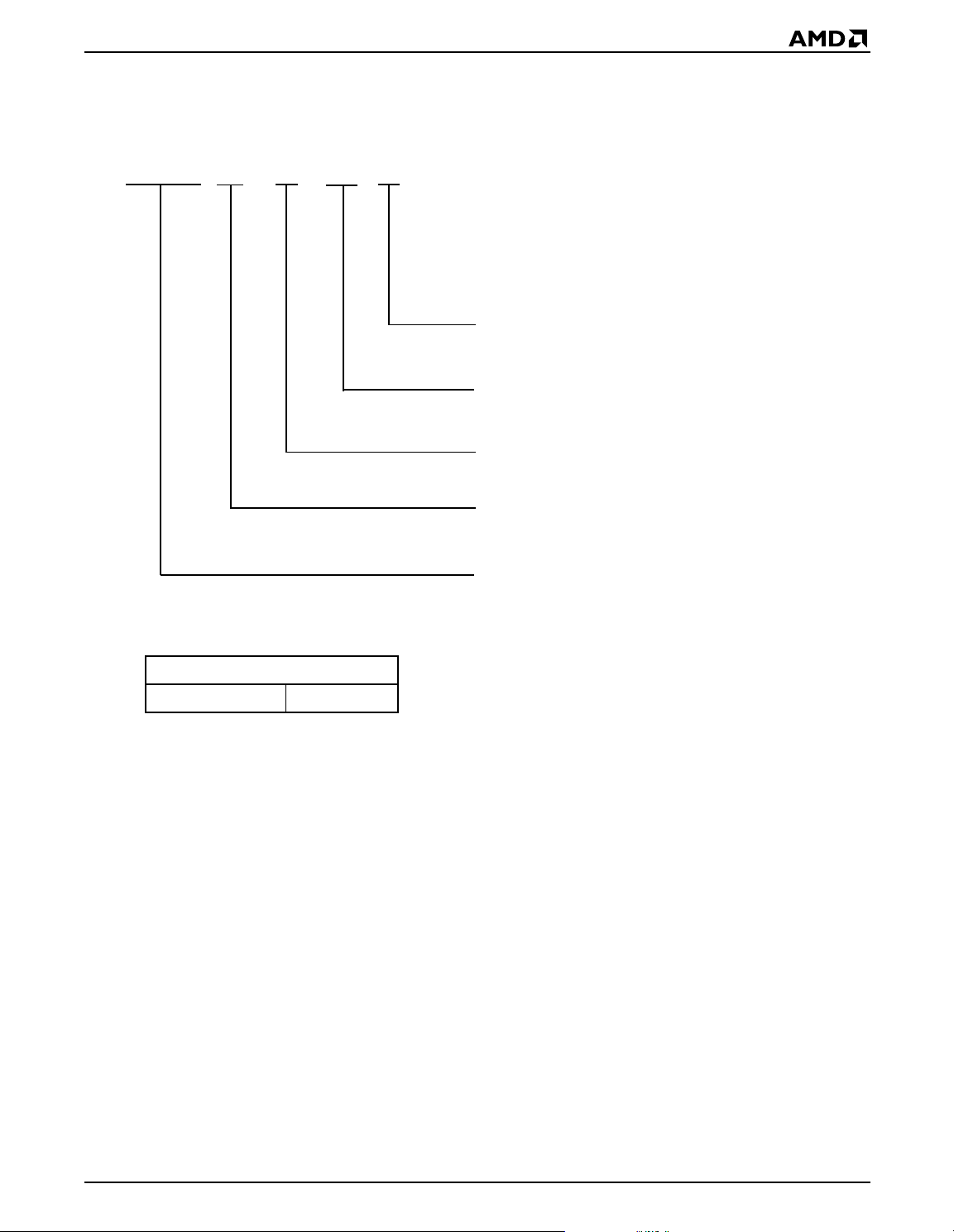
LOGIC SYMBOL
Management
Expansion
Port
Test and
Port
PRELIMINARY
V
DAT
JAM
ACK
COL
SELO
SELI[1:0]
SI
SO
SCLK
AMODE
STR
CRS_I
CRS
SI_D
CLK
RST
DD
Am79C985
LDA[4:0], LDB[4:0]
TXD+
TXD–
RXD+
RXD–
DO+
DO–
DI+
DI–
CI+
CI–
LDGA, LDGB
LDC[2:0]
ACT[7:0]
Twisted Pair
Ports
(4 Ports)
AUI
LED
Interface
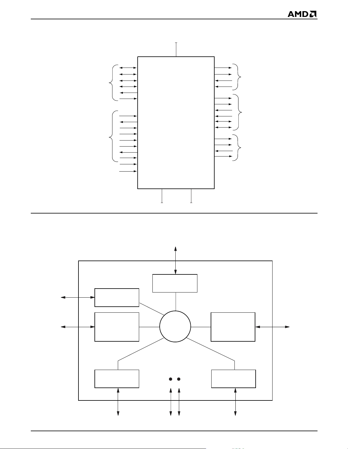
LOGIC DIAGRAM
LED
Port
Control
Port
DV
SS
AUI
Repeater
State
Machine
AV
SS
20651B-4
Expansion
Port
Twisted Pair
Port 0
Twisted Pair
Port 3
20651B-5
Am79C985 9
Page 10

PIN DESIGNATIONS (PL 084)
Listed by Pin Number
PRELIMINARY
Pin No.
1
2 TXD3- 23 STR 44 SCLK 65 LDB3
3 VDD 24 DVSS 45 VDD 66 LDA4
4 RXD0+ 25 CRS_I 46 ACT0 67 DVSS
5 RXD0- 26 SI_D 47 ACT1 68 LDB4
6 RXD1+ 27 VDD 48 ACT2 69 LDGA
7 RXD1- 28 RST 49 DVSS 70 LDGB
8 RXD2+ 29 CLK 50 ACT3 71 VDD
9 RXD2- 30 DVSS 51 ACT4 72 LDC0
10 RXD3+ 31 SELI_0 52 ACT5 73 LDC1
11 RXD3- 32 SELI_1 53 ACT6 74 LDC2
12 REXT 33 SELO 54 ACT7 75 VDD
13 AVSS 34 COL 55 LDA0 76 TXD0+
14 DI+ 35 DVSS 56 LDB0 77 TXD015 DI- 36 ACK 57 DVSS 78 AVSS
16 VDD 37 DAT 58 LDA1 79 TXD1+
17 CI+ 38 VDD 59 LDB1 80 TXD118 CI- 39 JAM 60 VDD 81 VDD
19 AVSS 40 CRS 61 LDA2 82 TXD2+
20 DO+ 41 DVSS 62 LDB2 83 TXD221 DO- 42 SI 63 DVSS 84 AVSS
Pin Name Pin No. Pin Name Pin No. Pin Name Pin No. Pin Name
TXD3+ 22 AMODE 43 SO 64 LDA3
10 Am79C985
Page 11

PIN DESIGNATIONS (PQR100)
Listed by Pin Number
PRELIMINARY
Pin No.
1
2 NC 27 NC 52 NC 77 NC
3 NC 28 NC 53 NC 78 NC
4 NC 29 NC 54 NC 79 NC
5 REXT 30 SELO 55 ACT7 80 VDD
6 AVSS 31 COL 56 LDA0 81 TXD0+
7 DI+ 32 DVSS 57 LDB0 82 TXD0-
8 DI- 33 NC 58 DVSS 83 AVSS
9 VDD 34 ACK 59 NC 84 TXD1+
10 CI+ 35 DAT 60 LDA1 85 TXD111 CI- 36 VDD 61 LDB1 86 VDD
12 AVSS 37 JAM 62 VDD 87 TXD2+
13 DO+ 38 CRS 63 LDA2 88 TXD214 DO- 39 DVSS 64 LDB2 89 AVSS
15 AMODE 40 SI 65 DVSS 90 TXD3+
16 STR 41 SO 66 LDA3 91 TXD317 DVSS 42 SCLK 67 LDB3 92 VDD
18 CRS_I 43 VDD 68 LDA4 93 RXD0+
19 SI_D 44 ACT0 69 DVSS 94 RXD020 VDD 45 ACT1 70 LDB4 95 RXD1+
21 RST 46 ACT2 71 LDGA 96 RXD122 NC 47 DVSS 72 LDGB 97 RXD2+
23 CLK 48 ACT3 73 VDD 98 NC
24 DVSS 49 ACT4 74 LDC0 99 RXD225 SELI_0 50 ACT5 75 LDC1 100 RXD3+
Pin Name Pin No. Pin Name Pin No. Pin Name Pin No. Pin Name
RXD3- 26 SELI_1 51 ACT6 76 LDC2
Note:
1. NC = No Connection.
Am79C985 11
Page 12

PRELIMINARY
PIN DESCRIPTION
AUI Port
DI+, DI–
Data In
Differential Input
DI± are differential, Manchester receiver pins. The
signals comply with IEEE 802.3, Section 7.
DO+, DO–
Data Out
Differential Output
DO± are differential, Manchester output driver pins. The
signals comply with IEEE 802.3, Section 7.
CI+, CI–
Collision Input
Differential Input/Output
CI± are differential, Manchester I/O signals. As an input,
CI is a collision-receive indicator . As an output, CI generates a 10-MHz signal if the eIMR+ device senses a
collision.
Twisted Pair Ports
TXD+
Transmit Data
Differential Output
TXD± are 10BASE-T port differential drivers (4 ports).
RXD+
Receive Data
Differential Input
RXD± are 10BASE-T port differential receive inputs
(4 ports).
0-3
0-3
, TXD–
, RXD–
0-3
0-3
Expansion Bus
DAT
Data
Input/Output/3-State
If the SELO
collision conditions, the eIMR+ device drives NRZ data
onto the DAT line, regenerating the preamble if necessary. During a collision, when JAM is HIGH, D A T is used
to differentiate between single-port (DAT=1) and multiport (DAT=0) collisions. DAT is an output when ACK is
asserted and the eIMR+ device’s ports are active; DAT
is an input when ACK is asserted and the ports are
inactive. If ACK is not asser ted, DAT is in the high-impedance state. It is recommended that DAT be pulled
up or down via a high value resistor.
JAM
Jam
Input/Output/3-State
The active eIMR+ device drives J AM HIGH, if it detects
a collision condition on one or more of its ports. The
and ACK pins are asserted during non-
state of the DAT pin is used in conjunction with JAM to
indicate a single port (DA T =1) or multiport (DAT=0) collision. J AM is in the high-impedance state if neither the
SEL
nor ACK signal is asserted. It is recommended that
JAM be pulled up or down via a high value resistor.
SELI
0-1
Select In
Input, Active LOW
When the expansion bus is configured f or Internal Arbitration mode, these signals indicate that another eIMR+
device is active; SELI0 or SELI1 is driven by SELO from
the upstream device. At reset, SELI0 selects between
the Internal Arbitration mode and the IMR+ mode of the
expansion bus; a HIGH selects the Inter nal Arbitration
mode and a LOW selects the IMR+ mode.
SELI_1 SELI_0
X 1 Internal
X 0 IMR+
Arbitration
Mode
SELO
Select Out
Output, Active LOW
If the expansion bus is configured f or Internal Arbitration
mode, an eIMR+ device drives this pin LOW when it is
active or when either of its SELI
pins is LOW. An
0-1
active eIMR+ device is defined as having one or more
ports receiving or colliding and/or is still transmitting
data from the internal FIFO, or extending a pack et to the
minimum of 96 bit times. When the expansion bus is
configured for IMR+ mode, SELO
is active when the
eIMR+ device is active (acquiring the functionality of the
REQ pin on the Am79C981 IMR+ device).
ACK
Acknowledge
Input/Output, Active LOW, Open Drain
This signal is asserted to indicate that an eIMR+ device
is active. It also signals to the other eIMR+ devices the
presence of a valid collision status on the JAM line and
valid data on the DAT line. When the eIMR+ device is
configured for Internal Arbitration mode, A
CK is an I/O,
and must be pulled to VDD via a minimum equivalent
resistance of 1 k
for IMR+ mode, A
When the eIMR+ device is configured
Ω.
CK is an input driven by an external
arbiter.
COL
Collision
Input/Output, Active LOW, Open Drain
When asserted, COL indicates that more than one
eIMR+ device is active. Each eIMR+ device generates
the Collision Jam sequence independently. When the
eIMR+ device is configured for Internal Arbitration
12 Am79C985
Page 13

PRELIMINARY
mode, COL
minimum equivalent resistance of 1 k
is an I/O and must be pulled to VDD via a
Ω.
When the
eIMR+ device expansion port is configured for IMR+
mode, COL
is an input driven by an external arbiter.
Management Port
AMODE
AUI Mode
Input
At reset, this pin sets the AUI port to either normal or
reversed mode. If AMODE is LOW at the rising edge of
, the AUI port is set to the normal mode; if AMODE
RST
is HIGH, the AUI port is set to the reversed mode.
CRS
Carrier Sense
Output
The states of the internal carrier-sense signals for the
AUI port and the four twisted-pair ports are output continuously on this pin. The output is a serial bit stream
synchronized to CLK. When two eIMR+ devices share
a common HIMIB device, CRS on the first de vice must
be connected to the CRS_I (input) of the second eIMR+
device.
CRS_I
Carrier Sense In
Input
CRS_I is used when two eIMR+ devices share a common HIMIB device. The CRS output from the first eIMR+
should be input to the second eIMR+ via this pin. Internally, the second eIMR+ appends the information on
CRS_I to its own carrier-sense information and outputs
the combined result to the HIMIB chip via its CRS pin.
At the rising edge of RST
eIMR+ device’ s management mode. CRS_I HIGH indicates that only a single eIMR+ device is connected to
the HIMIB chip. CRS_I LOW indicates that two eIMR+
devices are connected to a HIMIB chip.
SCLK
Serial Clock In
Input
Serial data (input or output) is clocked (in or out) on the
rising edge of the signal on this pin. SCLK is asynchronous to CLK and can operate at frequencies up to 10
MHz.
SI
Serial In
Input
The SI pin is used as a test/management serial input
port. Management commands are clocked in on this pin
synchronous to the SCLK input.
At reset, SI sets the state of the Automatic P olarity Reversal function. If SI is HIGH at the rising edge of RST,
, CRS_I is used to set the
Automatic Polarity Reversal is disabled. If SI is LOW at
the rising edge of RST
, Automatic Polarity Reversal is
enabled.
SI_D
Serial Input Append
Input
SI_D is used when two eIMR+ devices share a common
HIMIB device. The SO output from the first eIMR+ device should be input to the second eIMR+ chip via this
pin. Internally, the second eIMR+ chip appends the
SI_D data to its own serial data stream and outputs the
result to the HIMIB device via its SO pin.
When two eIMR+ devices are connected to a HIMIB
device, the HIMIB device has attribute counters for the
AUI port on only one of the eIMR+ devices. That eIMR+
device is referred to as the
other device is referred to as the
primary
secondary
eIMR+ device. The
eIMR+ de-
vice.
At the rising edge of RST
, the combination of CRS_I
and SI_D is used to set the eIMR+ device’s management mode. If CRS_I is HIGH, the state of SI_D is ignored and the eIMR+ device is configured as a single
eIMR+. If CRS_I is LOW, SI_D HIGH indicates that the
eIMR+ device is the secondary device. If CRS_I is LOW
and SI_D is LOW, the eIMR+ device is configured as
the primary device.
Two eIMR+ Devices
CRS_I SI_D
0
0
1
1
0
1
0
1
Single
eIMR+
Device
√
√
Primary
eIMR+
Device
√
Secondary
eIMR+
Device
√
SO
Serial Out
Output
The SO pin is used as a management command serial
output port. Responses to management commands are
clocked out on this pin synchronous to the SCLK input.
STR
Store
Input
The HIMIB device uses this input to communicate with
the eIMR+ device. STR connects to an internal pull-up
resistor. The resistance value is sufficiently high to allow
the STR pins of two eIMR+ devices to be connected
together without presenting an excessive load to the
HIMIB device.
Am79C985 13
Page 14

PRELIMINARY
LED Interface
LDA
LED Drivers
Output, Open Drain
LDA
respectively. LDA0 and LDB0 indicate the status of the
AUI port; LDA
four TP ports. The port attributes monitored by LDA
and LDB
LDGA
Global LED Driver, Bank A
Output, Open Drain
LDGA is the Global LED driver for LED Bank A. The
signal represents global CRS or COL conditions. In a
multiple-eIMR+ configuration, LDGA from each of the
eIMR+ devices can be tied together to drive a single
global LED in Bank A.
LDGB
Global LED Driver, Bank B
Output, Open Drain
LDGB is the Global LED driver for LED Bank B. The
signal represents global CRS or JAB conditions. In a
multiple eIMR+ configuration, LDGB from each of the
eIMR+ devices can be tied together to drive a single
global LED in Bank B.
LDC
LED Control
Input
These pins select the attributes that will be displayed
on LDA
grammed to display two attributes , the attribute associated with the periodic blink takes precedence.
ACT
Activity Display
Output, Open Drain
These signals drive the activity LEDs, which indicate
the percentage of network utilization. The displa y is updated every 250 ms.
, LDB
0-4
0-4
0-2
0-7
0-4
and LDB
are programmed by three pins, LDC
0-4
, LDB
0-4
drive LED Bank A and LED Bank B,
0-4
and LDB
1-4
, LDGA, and LDGB. If an LED is pro-
0-4
indicate the status of the
1-4
0-2
0-4
.
Miscellaneous Pins
RST
Reset
Input, Active LOW
When RST is LOW, the eIMR+ device resets to its default state. On the rising (trailing) edge of RST, the
eIMR+ also monitors the state of the SELI
AMODE pins, to configure the operating mode of the
device. In multiple eIMR+ systems, the falling (leading)
edge of the RST signal must be synchronized to CLK.
CLK
Master Clock In
Input
This pin is a 20-MHz clock input.
REXT
External Reference
Input
This pin is used for an internal current reference. It must
be tied to VDD via a 13-k
Ω resistor with 1% tolerance.
VDD
Power
Power Pin
This pin supplies power to the device.
AVSS
Analog Ground
Ground Pin
This pin is the ground reference for the differential
receivers and drivers.
DVSS
Digital Ground
Ground Pin
This pin is the ground reference for all the digital logic
in the eIMR+ device.
, SI, and
0-1
14 Am79C985
Page 15

PRELIMINARY
FUNCTIONAL DESCRIPTION
The Am79C985 eIMR+ device is a single-chip implementation of an IEEE 802.3/Ethernet repeater (or hub).
It is offered with four integr al 10BASE-T ports plus one
RAUI port comprising the basic repeater. The eIMR+
device is also expandab le, enabling the implementation
of high port count repeaters based on several eIMR+
devices.
The eIMR+ device interfaces directly with AMD’s
Am79C987 HIMIB device. This allows hardware designers to implement a fully managed multiport repeater, as specified by the IEEE 802.3 standard,
Section 19,
Repeaters
used as a chip set, the HIMIB device maintains complete repeater and per-port statistics, which can be accessed on demand through an 8-bit parallel interface.
The eIMR+ chip complies with the full set of repeater
basic functions as defined in Section 9 of ISO 8802.3
(ANSI/IEEE 802.3c). The basic repeater functions are
summarized in the paragraphs below.
Layer Management f or 10 Mbps Baseband
. When the eIMR+ and HIMIB devices are
Basic Repeater Functions
The Am79C985 chip implements the basic repeater
functions as defined by Section 9.5 of the ANSI/IEEE
802.3 specification.
Repeater Function
If any single network port senses the start of a valid
packet on its receive lines, the eIMR+ device will retransmit the received data to all other enabled network
ports (except when contention exists among any of the
ports or when the receive port is par titioned). To allow
multiple eIMR+ device configurations, the data will also
be repeated on the expansion bus data line (DAT).
Signal Regeneration
When retransmitting a packet, the eIMR+ device ensures that the outgoing packet complies with the IEEE
802.3 specification in terms of preamble structure and
timing characteristics. Specifically, data packets repeated by the eIMR+ device will contain a minimum of
56 preamble bits before the Start-of-Frame Delimiter . In
addition, the eIMR+ restores the voltage amplitude of
the repeated waveform to levels specified in the IEEE
802.3 specification. Finally, the eIMR+ device restores
signal symmetry to repeated data packets, removing jitter and distortion caused by the network cabling. Jitter
present at the output of the AUI port will be better than
0.5 ns; jitter at the TP outputs will be better than 1.5 ns .
The start-of-packet propagation delay for a repeater set
is the time delay between the first edge transition of a
data packet on its input port to the first edge transition
of the repeated packet on its output ports. The start-ofpacket propagation delay for the eIMR+ is within the
specification given in Section 9.5.5.1 of the IEEE 802.3
standard.
Jabber Lockup Protection
The eIMR+ device implements a built-in jabber protection scheme to ensure that the network is not disabled
by the transmission of excessively long data packets.
This protection scheme causes the eIMR+ device to interrupt transmission for 96 bit-times if the device has
been transmitting continuously for more than 65,536 bit
times. This is referred to as MAU Jabber Lockup Protection (MJLP). The MJLP status for the eIMR+ device
can be read through the Management Port, using the
Get MJLP Status command.
Collision Handling
The eIMR+ device will detect and respond to collision
conditions as specified in the IEEE 802.3 specification.
Repeater configurations consisting of multiple eIMR+
devices also comply with the IEEE 802.3 specification,
using status signals provided by the expansion bus. In
particular, a repeater based on one or more eIMR+ devices will handle the transmit collision and one-port-left
collision conditions correctly, as specified in Section 9
of the IEEE 802.3 specification.
Fragment Extension
If the total packet length received is less than 96 bits,
including preamble, the eIMR+ device will extend the
repeated packet length to 96 bits by appending a Jam
sequence to the original fragment.
Auto Partitioning/Reconnection
Any of the TP ports or the A UI port can be partitioned if
the duration or frequency of collisions becomes excessive. The eIMR+ device will continue to transmit data
packets to a partitioned port, but will not respond, as a
repeater, to activity on the partitioned port’s receiver.
The eIMR+ device will monitor the port and reconnect
it once certain criteria are met. The criteria for reconnection are specified by the IEEE 802.3 standard. In
addition to the standard reconnection algorithm, the
eIMR+ device implements an alternative reconnection
algorithm, which provides a more robust partitioning
function for the TP ports and/or AUI port. The eIMR+
device partitions each TP port and the AUI port separately and independently of other network ports.
The eIMR+ device will partition an enabled network
port if either of the following conditions occurs at that
port:
1. A collision condition exists continuously for more
than 2048 bit times. (AUI port—SQE signal active;
TP port—simultaneous transmit and receive).
2. A collision condition occurs during each of 32 con-
secutive attempts to transmit to that port.
In the AUI port, a collision condition is indicated by an
active SQE signal. In a TP port, a collision condition is
Am79C985 15
Page 16

PRELIMINARY
indicated when the port is simultaneously attempting to
transmit and receive.
Once a network port is par titioned, the eIMR+ device
will reconnect that port, according to the selected reconnection algorithm, as follows:
1. Standard reconnection algorithm—A data packet
longer than 512-bit times (nominal) is transmitted or
received by the partitioned port without a collision.
2. Alternative reconnection algorithm—A data packet
longer than 512-bit times (nominal) is transmitted by
the partitioned port without a collision.
A partitioned port can also be reconnected by disabling
and re-enabling the port.
All TP ports use the same reconnection algorithm; either they must all use the standard algorithm, or they
must all use the alternative reconnection algorithm.
Howev er, the reconnection algorithm for the AUI port is
programmed independently from that of the TP ports.
Detailed Functions
Reset
The eIMR+ device enters the reset state when the
reset (RST) pin is driven LOW. After the initial application of power , the RST pin must be held LO W for a minimum of 150 µs. If the RST pin is subsequently
asserted while power is maintained to the eIMR+ device, a reset duration of only 4 µs is required. This allows the eIMR+ device to reset its internal logic. During
reset, the eIMR+ registers are set to their default values. Also during reset, the eIMR+ device sets the output signals to their inactive state; that is, all analog
outputs are placed in their idle state, no bidirectional
signals are driven, all active-HIGH signals are driven
LOW and all active-LOW signals are driven HIGH. In a
multiple eIMR+ system, the reset signal must be synchronized to CLK. See Figure 13 in the
cations
section.
Systems Appli-
The eIMR+ device also monitors the state of the
SEL
I
, SI, CRS_I, SI_D, and AMODE pins on the ris-
0-1
ing (trailing) edge of RST to configure the operating
mode of the device.
Table 1 summarizes the state of the eIMR+ chip following reset.
AUI Port
The AUI Por t is fully compatible with the IEEE 802.3,
Section 7 requirement for an A UI port. It has the signals
associated with an AUI port: DO, DI, and CI.
The AUI port has two modes of operation: normal and
reverse. When configured for normal operation, the
functionality is that of an AUI port on a MAC (CI is an
input). When configured f or rev erse operation, the functionality is that of an AUI on a MAU (CI is an output).
The mode of the AUI port is set during the trailing (rising) edge of the reset pulse, by the state of the AMODE
pin. A LO W sets the AUI port to its normal mode (CI Input) and a HIGH sets the AUI port to its reverse (CI Output) mode.
The eIMR+ device can be connected directly to a MAC
through the AUI port. This requires that the AUI port be
configured for reverse operation. Refer to the
Applications
section for more details.
Systems
TP Port Interface
Twisted Pair Transmitters
TXD is a differential twisted-pair driver. When properly
terminated, TXD will meet the electrical requirements
for 10BASE-T transmitters as specified in IEEE 802.3,
Section 14.3.1.2.
The TXD signal is filtered on the chip to reduce harmonic content per IEEE 802.3, Section 14.3.2.1
(10BASE-T). Since filtering is perf ormed in silicon, TXD
can connect directly to a standard transformer, thereb y,
eliminating the need for external filtering modules.
Proper termination is shown in the
tions
section.
Systems Applica-
Table 1. eIMR+ States after Reset
Function State after Reset Pull Up/Pull Down
Active-LOW Outputs HIGH No
Active-HIGH Outputs LOW No
SO Output HIGH No
DAT, JAM HIGH IMPEDANCE Either
Transmitters (TP and AUI) IDLE No
Receivers (TP and AUI) ENABLED Terminated
AUI Partitioning/Reconnection Algorithm STANDARD ALGORITHM N/A
TP Partitioning/Reconnection Algorithm STANDARD ALGORITHM N/A
Link Test Functions for TP Ports ENABLED, TP PORTS IN LINK FAIL N/A
Automatic Receiver Polarity Reversal Function DISABLED IF SI PIN IS HIGH
ENABLED IF SI PIN IS LOW
N/A
16 Am79C985
Page 17

PRELIMINARY
Connection to Alternate Media
The eIMR+ device can be connected to the A UI port of
any MAU device. Thus, it can support 10BASE-2,
10BASE-5, and 10BASE-FL. To connect to an alternate
media type, on-chip filtering should be disabled. This
can be achieved by substituting the normal 110-Ω resistor connected across the TXD diff erential output with
a 500-Ω resistor. If on-chip filter ing is disabled at a TP
port, the Link Pulse must also be disabled. Ref er to the
section on
eIMR+ Management Commands
for pro-
gramming details.
Once port filtering is disabled, the TXD output will be a
square wavef orm and can be connected to the AUI port
of a transceiver . Some external components are necessary to correctly interface the TXD output to the transceiver .
Twisted Pair Receivers
RXD is a differential twisted-pair receiver. When properly terminated, RXD will meet the electrical requirements for 10BASE-T receivers as specified in IEEE
802.3, Section 14.3.1.3. The receivers do not require
external filter modules. Proper termination is shown in
the
Systems Applications
section.
The receiver’ s threshold voltage can be programmed to
an extended-distance mode. In this mode, the differential receiver’s threshold is reduced to allow a longer
cable than the 100 meters specified in the IEEE 802.3
standard. For programming details, refer to the
agement Commands
section.
Man-
Link Test
The integrated TP ports implement the Link Test function, as specified in the IEEE 802.3 10BASE-T standard. The eIMR+ device will transmit Link Test pulses
to any TP port after that port’s transmitter has been inactive for more than 8 ms to 17 ms. Conversely, if a TP
port does not receive any data packets or Link Test
pulses for more than 65 ms to 132 ms and the Link Test
function is enabled for that port, then that port will enter
the link-fail state. The eIMR+ device will disable a port
in link-fail state (i.e., disable repeater transmit and receive functions) until it receives either f our consecutive
Link Test pulses or a data packet.
The Link Test function can be disabled via the eIMR+
management port on a por t-by-por t basis, to allow the
eIMR+ device to operate with pre-10BASE-T networks
that do not implement the Link Test function. When the
Link Test function is disabled, the eIMR+ device will not
allow the TP port to enter link-fail state, even if no Link
Test pulses or data packets are being received. Note,
however, that the eIMR+ device will always transmit
Link Test pulses to all TP ports, regardless of whether
or not the port is enabled, partitioned, in link-fail state,
or has its Link Test function disabled. Separate management commands exist for enabling and disabling
the transmission of Link Test pulses on a port-by-port
basis.
Polarity Reversal
The TP ports can be programmed to receive data if a
wiring error results in a data packet being received at a
TP port with reversed polarity. This function will be enabled upon reception of a negative End Transmit Delimiter (ETD) or negative pulses and allows subsequent
packets to be received with the correct polarity. The polarity-reversal function is executed once following reset
or link-fail and can be programmed via the management port to be enabled or disabled on a port-by-port
basis. The function may be enabled or disabled, following a reset, depending on the level of the SI signal on
the rising edge of the RST pulse.
Visual Status Monitoring (LED) Support
The eIMR+ status port can be connected to LEDs to
facilitate the visual monitoring of repeater port status.
The status port has twelve output signals, LDA
LDB
, LDGA, and LDGB. LDA
0-4
and LDB
0-4
0-4
0-4
, and
represent the four TP ports and AUI port. LDGA and LDGB
are global indicators. Attributes that may be monitored
are Carrier Sense (CRS), Collision (COL), Partition
(PAR), Link Status (LINK), Loopback (LB), Port Disabled (DIS), and Jabber (JAB). Three control bits,
LDC
, select the particular attributes to be displayed
0-2
on the LEDs. Table 1 shows how the programming
combinations for LDC
control the attributes that will
0-2
be monitored.
Each LED drive pin (LDGA, LDGB, LDA
, and LDB
0-4
0-4
has two states: Off and LOW. When none of the selected attributes are true, the driver is off and the diode
is unlit. When an attribute is true, the driver is LO W , and
the corresponding LEDs in Bank A or Bank B will be lit.
Some of the settings (LDC2 = 1) include a blink function. This allows tw o attributes to be selected for a giv en
state on the pin. As an example when LDC
= 110,
0-2
the LDA outputs relating to TP ports will be solidly lit
when there is a link established at that port. However,
whenever there is activity on a port, the corresponding
LDA pin will switch on (LOW) and off at a period of 130
ms. Note that a partition on that port will also cause the
pin to go LOW.
On LDC settings that have two attributes for a state on
a pin (blink or solid-on), the attribute causing the output
to blink has priority. (Those attributes are shown in
Table 2 with a blink period specified next to it.) If an attribute has no blink period specified, the LED indicates
the attribute by being solidly lit.
)
Am79C985 17
Page 18

20651B-6
PRELIMINARY
Table 2. LED Attribute-Monitoring Program Options
LED Control
LDC
LDC
2
0
0 0 1 CRS COL LINK CRS LB CRS
0 1 0 Reserved (Note 5)
0 1 1 Reserved (Note 5)
1 0 0
1 0 1 COL JAB LINK (Note 3)
1 1 0 CRS COL LINK
1 1 1 CRS COL LINK (Note 4)
LDC
1
0
0 0 CRS COL LINK (Note 2) PAR LB PAR
CRS 260-ms blk COL 260-ms blk
Notes:
1. CRS = Carrier Sense, COL = Collision, JAB = Jabber, LINK = Link, LB = Loop Back, PAR = Partition, DIS = Port Disabled,
blk = Blink (Number = period of Blink).
2. For the LDC
setting of 000: If the port is partitioned, the LINK LED is off.
0-2
3. All LEDs blink 16 times at 260 ms per blink after reset.
4. All LEDs are on for approximately 4 seconds after reset.
5. LDC
= ‘010’ and ‘011’ are undefined.
0-2
Global LEDs TP LEDs AUI LEDs
LDGA
LDGB LDA
LINK
CRS 260-ms blk
CRS 512-ms blk
CRS 130-ms blk
PAR 1.56-s blk
1-4
LDB
1-4
PAR
COL 260-ms blk CRS 260-ms blk
PAR (Note 3) (Note 3)
PAR or DIS
COL (Note 4) (Note 4)
LDA
CRS 512-ms blk
CRS 130-ms blk
PAR 1.56-s blk
0
LDB
0
PAR
COL 260-ms blk
PAR (Note 3)
PAR or DIS
PAR (Note 4)
The LEDs can also be controlled via the management
port. The Enable Software Override commands turn
the LEDs on regardless of the attributes selected for
display through the LDC setting. Enable Software
Override of Bank A LEDs causes the LDA
and LDGA
0-4
pins to be driven LOW, and Enable Software Override
of Bank B LEDs causes the LDB
and LDGB pins to
0-4
be driven LOW. The blink rate is set by the Software
Override LED Blink Rate command. The periods are
off, 512 ms, 1560 ms, or solid on.
LED software override is executed in two stages, by
first issuing the blink rate (Software Override of LED
Blink Rate) and then issuing the command to enable
the particular por t LEDs (Enable Software Override of
Bank A/B LEDs). All port combinations selected for
software override control will reference the blink rate
last issued by the Software Override of the LED Blink
Rate command.
LDA
0-4
, LDB
, LDGA, and LDGB are open drain out-
0-4
put drivers that sink 12 mA of current to turn on the
LEDs. In a multiple eIMR+ configuration, the outputs
from the global LED drivers (LDGA and LDGB) of each
chip can be tied together to drive a single pair of global
status LEDs.
CRS and COL are extended to make it easier f or visual
recognition; that is, they will remain active for some
time even if the corresponding condition has expired.
Once carrier sense is active, CRS will remain active f or
a minimum of 4 ms. Once a collision is detected, COL
is active for at least 4 ms. The exception to this rule is
for selection LDC
= 111. For this selection, COL is
0-2
stretched to 100 µ s.
When LDC
tribute (LB) for the A UI port is display ed on LDA
= 000 or LDC
0-2
= 001, the loopback at-
0-2
. LB is
0
true when DO on the MAU is successfully looped back
to DI on the AUI port. LB is f alse (off) if a loopbac k error
is detected, or if the AUI port is disabled or in the reverse mode. Transmit carr ier sense is sampled at the
end of packet to determine the state of LB. The state of
LB remains latched until carrier sense is sampled again
for the next pac ket. The default/power-up state f or LB is
false (off).
Figure 1 shows the recommended connection of LEDs.
When LDA
0-4
, LDB
, LDGA, or LDGB are LOW, the
0-4
LED lights.
V
DD
eIMR+
LED
Interface
LDA[4:0]
LDB[4:0]
LDGA
LDGB
R
Typical
20651A-6
Figure 1. Visual Monitoring Application—Direct
LED Drive
18 Am79C985
Page 19

PRELIMINARY
Network Activity Display
The eIMR+ status port can drive up to eight LEDs to indicate the network-utilization level as a percentage of
bandwidth. The status por t uses eight dedicated outputs (ACT
) to drive a series of LEDs. The number of
0-7
LEDs in the series that will be lit increases as the
amount of network activity increases. ACT0 represents
the lowest level of activity; ACT7 represents the highest. ACT
are open-drain outputs that typically sink
0-7
12 mA of current to turn on the LEDs. See Figure 2.
Table 3 shows ACT
as a function of the percentage
0-7
of network utilization. The table uses a scale that is
more sensitive at low utilization levels. 100% utilization
represents the maximum number of events that could
occur in a given window of time.
The update rate and corresponding internal sampling
window for ACT[7:0] is 250 ms. During this sampling
window , a counter is used to count the number of times
repeater transmit activity is TRUE. The counter uses a
free-running clock which has the granularity to detect
the minimum packet size of 96 bit times.
Figure 3 shows the timing relationship between the
sampling window, counting clock, and transmit activity.
Table 3. Network Utilization
Number of LEDs
Lit by ACT
0-7
8 >80%
7 >64%
6 >32%
5 >16%
4 >8%
3 >4%
2 >2%
1 >1%
V
Percentage Utilization
DD
eIMR+
LED
Interface
ACT[0]
ACT[1]
ACT[2]
ACT[3]
ACT[4]
ACT[5]
ACT[6]
ACT[7]
20651A-7
20651B-7
Figure 2. Network Activity Display
.
latch data;
update display;
clear counter
counter is active
next counting cycle
Sampling
Window
Counting
Clock
Xmit
Activity
20651B-8
Figure 3. Activity Sampling
Am79C985 19
Page 20

PRELIMINARY
Expansion Bus Interface
The eIMR+ device expansion bus allows multiple
eIMR+ devices to be interconnected.
The expansion bus supports two modes of operation:
internal arbitration mode and IMR+ mode. The internal
arbitration mode uses a modified daisy-chain scheme
to eliminate the need for any external arbitration circuitry. The IMR+ mode maintains the full functionality of
the IMR+ (Am79C981) expansion bus and benefits
from minimum delays. In this mode, the eIMR+ device
requires external circuitry to handle arbitration for control of the bus.
The eIMR+ arbitration mode is determined at reset.
This occurs on the trailing edge of RST
state of SELI
, as illustrated in Figure 4.
0-1
according to the
The eIMR+ device can be connected to a HIMIB device ,
as described in the
eIMR+/HIMIB Interconnection
section. The connection to a HIMIB device is not dependent
on the mode of the expansion bus. In other words, the
eIMR+ device can be connected to a HIMIB device
whether the expansion bus is in internal-arbitration
mode or IMR+ mode.
Internal Arbitration Mode
The internal arbitration mode uses a daisy-chain (cascade) configuration. SELI
are arbitration inputs and
0-1
SELO is the arbitration output. SELO goes LOW when
there is activity on one or more of the eIMR+ ports, or
a SELI input is LOW. The SEL lines are connected as
shown in Figure 5. This technique allo ws activity indication to propagate down the chain to the end device. All
unused SELI inputs must be tied to VDD.
ACK and COL are global activity I/O pins. When the
eIMR+ device senses activity, it drives ACK LOW.
RST
SELI_0
SELI_1 SELI_0
X 1 Internal
X 0 IMR+
Mode Selection
Arbitration
Mode
20651B-9
Figure 4. Expansion Bus Mode Selection
An eIMR+ device drives COL LOW when it senses
more than one device is active; that is, if the device has
an active port AND a SELI input is LOW , OR both SELI
inputs are LOW.
In Boolean notation, the formula for COL is as follows:
COL = (Active port & (SELI1 + SELI0))+
(SELI1 & SELI0)
where
& represents the Boolean AND operation
+ represents the Boolean OR operation
ACK and COL are mutually e xclusive. If the eIMR+ device driving ACK senses COL LOW, the device will
deassert ACK.
DAT and JAM are synchronized to CLK. D AT is the repetition of data from any connected port (either TP or
AUI port) encoded in NRZ format. JAM is an internal
collision indicator. If J AM is HIGH, the active eIMR+ device has detected an internal collision across one or
more of its ports. When this occurs , the DAT signal distinguishes between single-port collisions and multiport
collisions. DAT = 1 indicates a single port collision;
DAT = 0 indicates a multiport collision.
The drive capabilities of the I/O signals on the expansion bus (DAT, JAM, A
CK, and COL) are sufficient to
allow seven eIMR+ devices to be connected together
without the use of external transceivers or buffers.
The maximum number of eIMR+ devices that can be
daisy chained is limited by the propagation delay of the
eIMR+ devices. In practice, the depth of the cascade is
limited to three eIMR+ devices, thus allowing a maximum of seven eIMR+ devices connected together via
this expansion bus as shown in Figure 5.
The active device will not drive the data line, DAT,
until one bit time (100 ns) after SELO goes LOW. This
is to avoid a situation where two devices drive DAT
simultaneously.
IMR+ Mode
In IMR+ mode, the expansion bus requires an external
arbiter. The arbiter allows only one eIMR+ device to
control the expansion bus. If more than one device attempts to take control, the arbiter terminates all access
and signals a collision condition.
In IMR+ mode, DAT and JAM retain the same functionality as in internal arbitration mode, but ACK and COL
are inputs to the eIMR+ device, driven by the external
arbiter. The arbiter should drive ACK LOW when exactly one eIMR+ device is active. It should drive COL
when more than one eIMR+ device is active. SELO is
an output from the eIMR+ device. It indicates that the
eIMR+ device has an active port and is requesting access to the bus. When A CK is HIGH, DAT and J AM are
in the high-impedance state. DAT and JAM go active
when ACK goes LOW. Refer to the
tions
section (Fig.14) for the configuration of IMR+
Systems Applica-
mode of operation.
Note: The IMR+ mode is recommended when arbitrating
between multiple boards.
20 Am79C985
Page 21

PRELIMINARY
V
DD
1kΩ
SELI_0
SELI_1
DAT
SELI_0
SELI_1
DAT
SELI_0
SELI_1
DAT
JAM
JAM
JAM
ACK
ACK
ACK
SELO
COL
SELO
COL
SELO
COL
SELI_0
SELI_1
DAT
SELI_0
SELI_1
DAT
JAM
JAM
ACK
ACK
SELO
COL
SELO
COL
SELI_0
SELI_1
DAT
JAM
ACK
SELO
COL
SELI_0
SELI_1
DAT
JAM
ACK
SELO
COL
Figure 5. Internal Arbitration—eIMR+ Devices in Cascade
Management Functions
The eIMR+ device receives management commands
in the form of byte-length data on the serial input pin,
SI. If the eIMR+ device is expected to provide data in
response to the command, it will send byte-length data
to the serial-output pin, SO. Both the input and output
data streams are clocked with the rising edge of the
SCLK signal. The byte-length data is in RS232 serialdata format; that is, one start bit followed by eight data
bits. The externally generated clock at the SCLK pin
Am79C985 21
20651B-10
may be either a free-running clock synchronized to the
input bit patterns, or a series of individual transitions
meeting the setup-and-hold times with respect to the
input bit pattern. If the latter method is used, 20 SCLK
clock transitions are required for management commands that produce SO data, and 14 SCLK clock transitions are required for management commands that
do not produce SO data.
Page 22

PRELIMINARY
eIMR+/HIMIB Interconnection
The eIMR+ device interfaces directly to the HIMIB device for full repeater manageability. To this end, the
eIMR+ device has a management port and a serial output that allows the HIMIB device to monitor port activity .
The eIMR+ device is designed to allow one or two
eIMR+ devices to operate with a single HIMIB device.
Because the HIMIB device can monitor nine ports (8 TP
ports & 1 AUI port), one of the eIMR+ AUI ports is not
managed (statistics not kept). When two eIMR+ de vices
are connected to a HIMIB device, one is designated the
primary device and the other is designated the secondary device. This designation serves to identify which
device has the managed AUI port. The primary device
has the managed AUI port and TP4-7. The secondary
device has the unmanaged A UI port and TP0-3. Figure
6 shows how the HIMIB and eIMR+ devices are interconnected.
V
DD
CRS_I
SI_D
When only one eIMR+ device is connected to a HIMIB
device, the AUI port is managed. The HIMIB device
treats the twisted-pair ports as TP0-3.
Although the HIMIB device does not monitor the AUI
port on the secondary eIMR+ device, the AUI port on
the secondary device defaults to enabled at reset. The
port can be disabled via the Secondary AUI Port Enable
command.
Management Port Interface
The eIMR+ management port is made up of six signals:
SI, SI_D, SO, CRS, CRS_I, and SCLK. SI is the serial
input from an external management module or the
HIMIB device. On the secondar y eIMR+ device, SI_D
is the response input from the primary eIMR+ device. It
is also used at reset to set the eIMR+ device as either
a primary or secondary device . CRS transmits the state
of the eIMR+ device’s internal carrier sense signals.
AUIM Port & TP[3:0]
eIMR+
CRS
SO
SCLK SI
DV
SS
HIMIB
SCLK
HIMIB
SCLK
CRS
SI
SO
CRS
AUIM Port & TP[7:4]
CRS_I
(Primary)
SI_D
SI
SO
a) One eIMR Device Connected to a HIMIB
eIMR+
CRS
SCLK SI
b) Two eIMR Devices Connected to a HIMIB
SO
Figure 6. eIMR-to-HIMIB Connection
AUIU Port & TP[3:0]
CRS_I
(Secondary)
SI_D
eIMR+
CRS
SCLK SI
SO
20651B-11
22 Am79C985
Page 23

PRELIMINARY
When two eIMR+ devices are connected to one HIMIB
device, the secondary device transmits the status of its
TP ports, then transmits the status of the primary eIMR+
TP ports and AUI port (CRS and CI). Note that the secondary device does not transmit the status of its AUI
port. At Reset, the secondary device (and single eIMR+
device) internally synchronizes the CRS stream to begin
with the AUI CI bit. SO is the eIMR+ de vice response to
a Get command.
The pins SI_D and CRS_I are multi-purpose pins. Their
primary pur pose is management input to the primary
eIMR+ device. They are also used to set the management mode of the eIMR+ device. The mode is set on the
rising edge of RST
. The settings are shown in T able 4.
Following reset, the eIMR+ de vices retain their management designations. Howe ver , CRS_I and SI_D return to
their management port functions.
Command/Response Timing
Figure 7 shows the command/response timing. At the
end of a GET command, the eIMR+ device waits two
SCLK cycles and then transmits the response on SO.
The secondary eIMR+ device stores the data received
on the SI_D input (from the primary eIMR+ device) in
an internal register. When it has transmitted D3 data, it
appends the received response to the end of the SO
signal.
Following reset, after the eIMR+ de vices hav e been assigned their primary and secondary designation, SO
and SI_D return to their management-port functions.
Port Activity
In addition to providing a means for receiving commands and sending data in response to those commands, the management port includes a CRS signal
that transmits the state of the eIMR+ device’s internal
carrier-sense signals.
When two eIMR+ devices are connected to one
Am79C987 HIMIB device (as shown in the
Applications
section), CRS_I of the secondary device
System
receives the following signals from the primary device:
the carrier-sense signals of the AUI port, the CI-bit status of the AUI port, and the carrier-sense signals of the
TP ports. The secondary device transmits the status of
the AUI port (CRS and CI) for the primary device, the
status of its own TP ports (TP0-TP3), and then the status of the primary device’s TP ports (TP4-TP7). The
status of the AUI port of the secondary device is not
retransmitted (see Figure 8).
Table 4. eIMR+ Device Management Designations
Two eIMR+ Devices
CRS_I SI_D Single eIMR+ Device Primary eIMR+ Device Secondary eIMR+ Device
0 0
0 1
1 0
1 1
SCLK
SO
SO
Note: For SO on the Primary device, D[3:0] corresponds to TP[7:4].
SI
ST D0 D1 D2 D3 D4 D5 D6 D7
Primary eIMR+ Device or
Single eIMR+ Device
Secondary eIMR+ Device
√
√
ST D0 D1 D2 D3
ST D0 D1 D2 D3 D4 D5 D6 D7
√
√
20651B-12
Figure 7. Management Get Command/Response
Am79C985 23
Page 24

CLK
TCLK
CRS
Secondary
CRS
Primary*
CRS
One eIMR+ Device
PRELIMINARY
CP T0 T1 T2 T3 T4 T5 T6 T7
AP
AP
CPT4 T5 T6 T7
C A T0 T1 T2 T3
*
Shows actual output stream to secondary device.
Figure 8. Port Activity Signals with Am79C987 HIMIB Device
Management Commands
The following section details the operation of each
management commands available in the eIMR+ device. In all cases, the individual bits in each command
are shown with the most-significant bit (bit 7) on the left
and the least-significant bit (bit 0) on the right. Table 5
and Table 6 show a summary of default states and a
summary of management commands, respectively.
Note: Data is transmitted and received on the serial
data lines least-significant bit first and most-significant
bit last.
20651B-13
Table 5. Summary of Default States after Reset
eIMR+ Programmable Option—
CSA
Off
AUI Partitioning Algorithm Normal
TP Partitioning Algorithm Normal
AUI/TP Port Enabled
Link Test Enabled
Link Pulse Enabled
Automatic Receiver Polarity
Reversal
State of SI at reset
Extended Distance Mode Disabled
Blink Rate Off
Software Override of LEDs Disabled
24 Am79C985
Page 25

PRELIMINARY
Table 6. Management Port Command Summary
SO Data
Single eIMR+
Commands
SI Data
Device
Set (Write Commands)
eIMR+ Chip Programmable Options
0000 1CSA
Alternate AUI Partitioning Algorithm 0001 1111
Alternate TP Partitioning Algorithm 0001 0000
Primary AUI Port Disable 0010 1111
Secondary AUI Port Disable 0010 1110
Primary AUI Port Enable 0011 1111
Secondary AUI Port Enable 0011 1110
TP Port Disable 0010 0###
TP Port Enable 0011 0###
Disable Link Test Function (per TP port) 0100 0###
Enable Link Test Function (per TP port) 0101 0###
Disable Link Pulse (per TP port) 0100 1###
Enable Link Pulse (per TP port) 0101 1###
Disable Automatic Receiver Polarity Reversal
(per TP port)
Enable Automatic Receiver Polarity Reversal
(per TP port)
Disable Receiver Extended Distance Mode
(Per TP port)
Enable Receiver Extended Distance Mode
(Per TP port)
Disable Software Override of LEDs
(Per Port - AUI & TP)
Enable Software Override of Bank-A LEDs
(Per Port - AUI & TP, Global)
Enable Software Override of Bank-B LEDs
(Per Port - AUI & TP, Global)
0110 0###
0111 0###
0110 1###
0111 1###
1001 ####
1011 ####
1100 ####
Software Override LED Blink Rate 1110 1###
Get (Read Commands)
AUI Port Status (B, S, and L Cleared)
AUI Port Status (B Cleared)
AUI Port Status (S, L, Cleared)
AUI Port status (None Cleared)
TP Port Partitioning Status
1000 1111 PBSL 0000 0000 PBSL PBSL
1000 1101 PBSL 0000 0000 PBSL PBSL
1000 1011 PBSL 0000 0000 PBSL PBSL
1000 1001 PBSL 0000 0000 PBSL PBSL
1000 0000 0000 C3..C0 0000 C7..C4 C7..C0
Bit Rate Error Status of TP Ports 1010 0000 0000 E3..E0 0000 E7..E4 E7..E0
Link Test Status of TP Ports 1101 0000 0000 L3..L0 0000 L7..L4 L7..L0
Receive Polarity Status of TP Ports 1110 0000 0000 P3..P0 0000 P7..P4 P7..P0
MJLP Status 1111 0000 M000 0000 0000 M000 M
Version 1111 1111 0000 0011 0000 0011 0011
SO Data
Primary
SO Data
Secondary
000 MS000
P
PBSL
P
PBSL
P
PBSL
P
PBSL
P
0011
P
S
S
S
S
S
Am79C985 25
Page 26

PRELIMINARY
SET (Write Commands)
Chip Prog
SI Data 0000 1CSA
SO Data (Pri) None
SO Data (Sec) None
The eIMR+ chip programmable options can be enabled
(or disabled) by setting (or resetting) one or more of the
C, S, and A bits in the command string. The three programmable options are C - CI Reporting, S - AUI test
mask, and A - Alternate port activity monitor (PAM)
function.
rammable Options
C HIMIB Connection
This bit, when set, indicates to the eIMR+ device that it
is connected to a HIMIB device.
S AUI SQE Test Mask
Setting this bit allows the eIMR+ chip to ignore activity
on the CI signal pair, during the SQE test window, following a transmission on the AUI port. Enabling this
function does not prevent the reporting of this condition by the eIMR+ device. The two functions operate
independently.
The SQE Test Window, as defined in IEEE 802.3 (Section 7.2.2.2.4) is from 6 bit times to 34 bit times (0.6 µs
to 3.4 µs). This includes the delay introduced by a 50m AUI. CI activity that occurs outside this window is not
ignored and is treated as a true collision.
A Alternate Port Activity Monitor Function
Setting this bit causes the Port Activity Monitor (PAM)
function to be altered such that the CRS data is presented unmodified. In default operation, CRS is
masked if the port is either disabled or partitioned. Note
that the HIMIB device resets this bit (default operation).
nate AUI Partitioning Algorithm
Alter
SI Data 0001 1111
SO Data (Pri) None
SO Data (Sec) None
Invoking this command sets the partition/reconnection
scheme for the A UI port to the alternate (transmit-only)
reconnection algorithm. To return the AUI port to the
standard (transmit or receive) reconnection algorithm,
it is necessary to reset the eIMR+ device. The standard
partitioning algorithm is selected on reset. If two eIMR+
devices are connected, this command sets both AUI
ports.
nate TP Partitioning Algorithm
Alter
SI Data 0001 0000
SO Data (Pri) None
SO Data (Sec) None
Invoking this command sets the partition/reconnection
scheme for the TP ports to the alternate (transmit-only)
reconnection algorithm. To return the TP ports to the
standard (transmit or receive) reconnection algorithm,
it is necessary to reset the eIMR+ device. The standard
partitioning algorithm is selected on reset.
imary AUI Port Disable
Pr
SI 0010 1111
SO Data (Pri) None
SO Data (Sec) None
This command disables the AUI port on the primar y
eIMR+ device. Subsequently the eIMR+ chip will ignore all inputs to this port and will not transmit a DAT or
JAM pattern on the AUI port. Disabling the AUI port
also sets the partitioning state machine of the AUI port
to the idle state. Therefore , a partitioned port can be reconnected by first disabling the AUI port and then enabling the AUI port.
The AUI port on the primary eIMR+ device defaults to
enabled on reset.
Secondar
SI Data 0010 1110
SO Data (Pri) None
SO Data (Sec) None
This command disables the AUI port on the eIMR+ device designated as the secondary HIMIB attachment.
Subsequently the eIMR+ chip will ignore all inputs to
this port and will not transmit a DAT or JAM pattern on
the AUI port. Disabling the AUI port also sets the partitioning state machine of the AUI port to the idle state.
Therefore, a partitioned port can be reconnected by first
disabling the AUI port and then enabling the AUI port.
The AUI port on the secondary eIMR+ device defaults
to enabled on reset.
imary AUI Port Enable
Pr
SI 0011 1111
SO Data (Pri) None
SO Data (Sec) None
This command enables the AUI port on the primary
eIMR+ device.
Secondar
SI Data 0011 1110
SO Data (Pri) None
SO Data (Sec) None
This command enables the AUI port on the eIMR+ device designated as the secondary HIMIB attachment.
When enabled, the secondary AUI port is fully functional, and can be controlled by the serial/management
interface. However, when used with the Am79C987 device, no status is displayed f or this port since the HIMIB
device does not manage this port. At reset, this port is
enabled.
y AUI Port Disable
y AUI Port Enable
26 Am79C985
Page 27

PRELIMINARY
ort Disable
TP P
SI Data 0010 0###
SO Data (Pri) None
SO Data (Sec) None
This command disables the TP port designated by the
three least-significant bits of the command byte. Subsequently the eIMR+ chip will ignore all inputs to the
designated port and will not transmit a DAT or JAM pattern on that port. Disabling the TP port also sets the
partitioning state machine of that por t to the idle state.
Therefore, a partitioned port can be reconnected by first
disabling the port and then enabling it. Designated port
values of b111 through b100 in the command byte correspond to TP7 through TP4 in the primary eIMR+ device. Designated port values of b011 through b000 in
the command byte correspond to TP3 through TP0 in
the secondary eIMR+ device.
ort Enable
TP P
SI Data 0011 0###
SO Data (Pri) None
SO Data (Sec) None
This command enables the TP port designated by the
three least-significant bits of the command byte. Designated port values of b111 through b100 in the command
byte correspond to TP7 through TP4 in the primary
eIMR+ device. Designated port values of b011 through
b000 in the command byte correspond to TP3 through
TP0 in the secondary eIMR+ device.
le Link Test Function (per TP port)
Disab
SI Data 0100 0###
SO Data (Pri) None
SO Data (Sec) None
This command disables the Link test function of the TP
port designated by the three least-significant bits of the
command data. As a consequence of this, the port will
no longer be disconnected if it fails the Link Test. If a
port has the Link Test disabled, reading the Link Test
Status indicates a ‘Link Pass’. Designated port values
of b111 through b100 in the command byte correspond
to TP7 through TP4 in the primary eIMR+ device. Designated port values of b011 through b000 in the command data correspond to TP3 through TP0 in the
secondary eIMR+ device.
le Link Test Function (per TP port)
Enab
SI Data 0101 0###
SO Data (Pri) None
SO Data (Sec) None
This command enables the Link test function of the TP
port designated by the three least-significant bits of the
command data. As a consequence of this, the port is
disconnected if it fails the Link Test. Designated port
values of b111 through b100 in the command byte correspond to TP7 through TP4 in the primary
eIMR+ device. Designated port values of b011 through
b000 in the command data correspond to TP3 through
TP0 in the secondary eIMR+ device.
le Link Pulse (Per TP Port)
Disab
SI Data 0100 1###
SO Data (Pri) None
SO Data (Sec) None
This command disables the transmission of the Link
pulse on the TP port designated by the three least-significant bits of the command byte. Designated port values of b111 through b100 in the command byte
correspond to TP7 through TP4 in the pr imary eIMR+
device. Designated port values of b011 through b000 in
the command data correspond to TP3 through TP0 in
the secondary eIMR+ device.
le Link Pulse (Per TP Port)
Enab
SI Data 0101 1###
SO Data (Pri) None
SO Data (Sec) None
This command enables the transmission of the Link
pulse on the TP port designated by the three least-significant bits of the command byte. Designated port values of b111 through b100 in the command byte
correspond to TP7 through TP4 in the pr imary eIMR+
device. Designated port values of b011 through b000 in
the command byte correspond to TP3 through TP0 in
the secondary eIMR+ device.
le Automatic Receiver Polarity Reversal (Per TP
Disab
Port)
SI Data 0110 0###
SO Data (Pri) None
SO Data (Sec) None
This command disables the Automatic Receiver Polarity Reversal function for the TP port designated by the
three least-significant bits in the command byte. If this
function is disabled on a TP port receiving with rev ersed
polarity (due to a wiring error), the TP port will fail the
Link Test due to the incorrect polarity of the received
Link pulses. Designated port values of b111 through
b100 in the command byte correspond to TP7 through
TP4 in the primary eIMR+ device. Designated port values of b011 through b000 in the command byte correspond to TP3 through TP0 in the secondary eIMR+
device.
The state of Automatic P olarity Re versal function is set
by SI on reset. If SI is HIGH at the rising edge of RST
the eIMR+ device disables A utomatic Polarity Re versal.
If SI is LOW at the rising edge of RST , the eIMR+ de vice
enables Automatic Polarity Reversal.
,
Am79C985 27
Page 28

PRELIMINARY
le Automatic Receiver Polarity Reversal (Per TP
Enab
Port)
SI Data 0111 0###
SO Data (Pri) None
SO Data (Sec) None
This command enables the Automatic Receiv er P olarity
Reversal function f or the TP port designated by the three
least-significant bits in the command byte. If enabled in
a TP port, the eIMR+ chip will automatically invert the
polarity of that port’s receiver circuitry if the TP port is
detected as having reversed polarity (due to wiring error). After reversing the receiver polarity, the TP port
could then receive subsequent (rev erse polarity) packets
correctly. Designated port values of b111 through b100
in the command byte correspond to TP7 through TP4 in
the primary eIMR+ device. Designated port values of
b011 through b000 in the command byte correspond to
TP3 through TP0 in the secondary eIMR+ device.
le Receiver Extended Distance Mode (Per TP
Disab
Port)
SI Data 0110 1###
SO Data (Pri) None
SO Data (Sec) None
This command disables the Receiver Extended Distance Mode and restores the RXD circuit of the transceiver to normal squelch levels for the TP-port driver
designated by the three least-significant bits of the command data. Designated port values of b111 through
b100 in the command byte correspond to TP7 through
TP4 in the primary eIMR+ device. Designated port values of b011 through b000 in the command byte correspond to TP3 through TP0 in the secondary eIMR+
device.
le Receiver Extended Distance Mode (Per TP
Enab
Port)
SI Data 0111 1###
SO Data (Pri) None
SO Data (Sec) None
This command modifies the RXD circuit of the transceiver for the TP-por t driver designated by the three
least-significant bits of the command data. The RXD
squelch-threshold value is lowered to accommodate
signal attenuation associated with lines longer than 100
meters. Designated port values of b111 through b100
in the command byte correspond to TP7 through TP4
in the primary eIMR+ device. Designated port values of
b011 through b000 in the command byte correspond to
TP3 through TP0 in the secondary eIMR+ device. At
reset, Receiver Extended Distance Mode is disabled
and the RXD circuit defaults to normal squelch-threshold values.
le Software Override of LEDs
Disab
(Per Port - AUI and TP, Global)
SI Data 1001 ####
SO Data (Pri) None
SO Data (Sec) None
This command Disables software override of the Port
LEDs.
Individual LEDs and combinations of LEDs can be selected via the lower four bits of the command byte, as
follows:
####
0000-0111 TP0 - TP7
1000 Primary AUI
1001 Secondary AUI
1010 Both AUI ports
1011 All TP ports
1100 All ports
1101 Primary Global
1110 Secondary Global
1111 All Global
Following command e x ecution, the attributes displa y ed
on the LEDs will be determined by LDC
override of LEDs is disabled after reset.
le Software Override of Bank-A LEDs (Per Port -
Enab
Port(s) affected
. Software
0-2
AUI and TP, Global)
SI Data 1011 ####
SO Data (Pri) None
SO Data (Sec) None
This command forces the LEDs in Bank A to blink. Individual LEDs and combinations of LEDs can be selected via the lower four bits of the command byte, as
follows:
####
0000-0111 TP0 - TP7
1000 Primary AUI
1001 Secondary AUI
1010 Both AUI ports
1011 All TP ports
1100 All ports
1101 Primary Global
1110 Secondary Global
1111 All Global
The designated LED drivers(s) will switch between
LOW and ‘off’ at the rate set by the Software Override
Blink Rate command. Enable Software Override of
Bank A LEDs references the blink rate last issued, and
overrides any other attribute specified by LDC
ware override of LEDs is disabled after reset.
Port(s) affected
0-2
. Soft-
28 Am79C985
Page 29

PRELIMINARY
le Software Override of Bank-B LEDs (Per Port -
Enab
AUI and TP, Global)
SI Data 1100 ####
SO Data (Pri) None
SO Data (Sec) None
This command forces the LEDs in Bank B to blink. Individual LEDs and combinations of LEDs can be selected via the lower four bits of the command byte, as
follows.
####
Port(s) affected
0000-0111 TP0 - TP7
1000 Primary AUI
1001 Secondary AUI
1010 Both AUI ports
1011 All TP ports
1100 All ports
1101 Primary Global
1110 Secondary Global
The designated LED drivers(s) will switch between
LOW and ‘off’ at the rate set by the Software Override
of LED Blink Rate command. Enab le Software Override
of Bank B LEDs references the blink rate last issued,
and overrides any other attribute specified by LDC
0-2
Software override of LEDs is disabled after reset.
are Override of LED Blink Rate
Softw
SI Data 1110 1###
SO Data (Pri) None
SO Data (Sec) None
This command sets the blink Period of the LEDs with
Software Override enabled. The duty cycle is 50%. This
command defaults to ‘off’ at reset.
Setting
Blink Period
1110 1000 Off
1110 1001 512 ms
1110 1010 1560 ms
1110 1011 Solid On
These settings apply to the blink rate for both Bank A
and Bank B. This command must precede the Enable
Software Override of Bank A/B LEDs command. All LED
combinations selected for software override will reference the blink rate last issued.
Get (Read Commands)
UI Port(s) Status
A
SI Data 1000 1111
SO Data (Sec) PBSLP PBSL
S
SO Data (Pri) 0000 PBSL
SO Data (Single) PBSL 0000
The combined AUI status of the eIMR+ de vice(s) allows
a single instruction to be used to monitor the AUI port(s).
The four local status bits are:
P Partitioning Status
This bit is ‘0’ if the AUI port is partitioned and ‘1’ if the
AUI port is connected.
B Bit Rate Error
This bit is set to ‘1’ if there is an instance of FIFO overflow or underflow. The bit is cleared when the eIMR+
device is read.
S SQE T est Status
This bit is set to ‘1’ if the SQE test error is detected by
the eIMR+ chip. The bit is cleared when the status is
read.
L Loopback Error
The MAU attached to the AUI por t is required to loopback data transmitted to DO onto the DI circuit. If the
loopback carrier is not detected by the eIMR+ device,
this bit is set to ‘1’. This bit is cleared when the status
is read.
If a single eIMR+ device is connected to a HIMIB device ,
SO is PBSL 0000. If two eIMR+ devices are connected
.
to a HIMIB device, SO on the primary device is 0000
PBSLP, and SO on the secondary device is PBSL
PBSLS. The subscr ipt (P) indicates the statistics of the
primary eIMR+ device and the subscript (S) indicates
the statistics of the secondary eIMR+ device.
nate AUI Port(s) Status
Alter
There are three further variations of the AUI Port Status
Command allowing selective clearing of a combination
of B,S, and L bits. These are the following:
Alternate 1: B is not cleared, S and L are Cleared
SI Data 1000 1011
SO Data (Sec) PBSLP PBSL
S
SO Data (Pri) 0000 PBSL
SO Data (Single) PBSL 0000
Alternate 2: S and L are not cleared, B is Cleared
SI Data 1000 1101
SO Data (Sec) PBSLP PBSL
S
SO Data (Pri) 0000 PBSL
SO Data (Single) PBSL 0000
Alternate 3: None of S, B, and L are Cleared
SI Data 1000 1001
SO Data (Sec) PBSLP PBSL
S
SO Data (Pri) 0000 PBSL
SO Data (Single) PBSL 0000
P
Am79C985 29
Page 30

PRELIMINARY
ort Partitioning Status
TP P
SI Data 1000 0000
SO Data (Sec) 0000 P3..P0,
P7..P0 (output to HIMIB)
SO Data (Pri) 0000 P7..P4
SO Data (Single) 0000 P3..P0
Pn = 0 TP Port Partitioned
Pn = 1 TP port Connected
where n is a port number in the range 0-7
The response to this command gives the partitioning
status of all four TP ports. If a port is disabled, reading
its partitioning status will indicate that it is connected. If
two eIMR+ devices are connected together , the secondary device indicates the status of all eight TP ports.
P7...P4 correspond to the four ports of the primary
device. P3..P0 correspond to the four por ts of the secondary device.
Bit Rate Error Status of
SI Data 1010 0000
SO Data (Sec) 0000 E3..E0,
SO Data (Pri) 0000 E7..E4
SO Data (Single) 0000 E3..E0
En = 0 No Error
En = 1 FIFO Overflow
where n is a port number in the range 0-7.
The response to this command gives the bit-rate-over-
flow or underflow (data rate mismatch) condition of all
the TP ports. A 1 indicates that the FIFO has overflow ed
or underflowed due to the amount of data received by
the corresponding port. If two eIMR+ devices are connected together, the secondary device indicates the status of all eight TP ports. E7...E4 correspond to the four
ports of the primar y device. E3...E0 correspond to the
four ports of the secondary device.
Test Status of TP ports
Link
SI Data 1101 0000
SO Data (Sec) 0000 L3..L0,
SO Data (Pri) 0000 L7..L4
SO Data (Single) 0000 L3..L0
Ln = 0 TP Port n in Link Test Failed
Ln = 1 TP port n in Link Test Passed
where n is a port number in the range 0-7.
The response to this command gives the Link Test sta-
tus of all the TP ports. A disabled port continues to report
Link Test status. Re-enabling the port causes the port
to be placed in the Link Test Fail state. If two eIMR+
devices are connected together, the secondary device
indicates the status of all eight TP ports. L7..L4 correspond to the four ports of the primary device. L3..L0
correspond to the four ports of the secondary device.
TP Ports
E7..E0 (output to HIMIB)
L7......L0 (output to HIMIB)
e Polarity Status of TP Ports
Receiv
SI Data 1110 0000
SO Data (Sec) 0000 P3......P0,
P7.....P0 (output to HIMIB)
SO Data (Pri) 0000 P7......P4
SO Data (Single) 0000 P3......P0
Pn = 0 TP Port n Polarity Correct
Pn = 1 TP port n Polarity Reversed
where n is a port number in the range 0-7
The response to this command gives the Received Po-
larity status of all the TP ports. If the polarity is detected
as reversed for a TP port, then the eIMR+ device will
set the appropriate bit in this command’s result only if
the Polarity Reversal Function is enabled for that port.
If two eIMR+ devices are connected together, the
secondary device indicates the status of all eight TP
ports. P7...P4 correspond to the four ports of the primary
device. P3..P0 correspond to the four por ts of the secondary device.
MJLP Status
SI Data 1111 0000
SO Data (Sec) M000 0000,
MP000 MS000 (to HIMIB)
SO Data (Pri) 0000 M000
SO Data (Single) M000 0000
Each eIMR+ device contains an independent MA U Jabber Lock Up Protection timer. The timer is designed to
inhibit the transmit function of the eIMR+ device if it has
been transmitting continuously for more than 65536 bit
times. This bit remains set and is only cleared when the
MJLP status is read using this command. If two eIMR+
devices are connected together, the secondary device
will indicate the status of both devices (MP is the status
of the primary device; MS is the status of the secondary
device).
ersion
V
SI Data 1111 1111
SO Data (Sec) 0000 0011,
0011P 0011S (to HIMIB)
SO Data (Pri) 0000 0011
SO Data (Single) 0000 0011
The response to this command gives the version of the
eIMR+ device. 0011 w as chosen to help distinguish the
eIMR+ device from the IMR (Am79C980) and the IMR+
(Am79C981) devices. If two eIMR+ devices are connected together, the secondary device will indicate the
version of the primary device in the upper four bits of
the SO byte, and its own version number in the lower
four bits.
30 Am79C985
Page 31

PRELIMINARY
SYSTEMS APPLICATIONS
eIMR+ to TP Port Connection
The eIMR+ device provides a system solution
to designing non-managed multiport repeaters. The
eIMR+ device connects directly to AC coupling modules for a 10BASE-T hub. Figure 9 shows the simplified connection.
Twisted Pair Transmitters
TXD signals need to be properly terminated to meet the
electrical requirement for 10BASE-T transmitters.
Proper termination is shown in Figure 10 which consists
eIMR+
TXD0+
TXD0–
RXD0+
RXD0–
TXD1+
TXD1–
RXD1+
RXD1–
110 Ω
100 Ω
110 Ω
100 Ω
of a 110-Ω resistor and a 1:1 transformer. The load is a
twisted-pair cable that meets IEEE 802.3, Section 14.4
specifications. The cable is terminated at the opposite
end by 100 Ω.
Twisted Pair Receivers
RXD signals need to be properly terminated to meet
the electrical requirements for 10BASE-T receivers.
Proper termination is shown in Figure 11. Note that the
receivers do not require external filter modules.
TP Connector
1:1
1:1
TP Connector
1:1
1:1
TP Connector
1:1
1:1
TP Connector
1:1
1:1
20651B-14
RST
CLK
TXD2+
TXD2–
RXD2+
RXD2–
TXD3+
TXD3–
RXD3+
RXD3–
110 Ω
100 Ω
110 Ω
100 Ω
Figure 9. Simplified 10BASE-T Connection
TXD+
110Ω
TXD-
1:1
Twisted Pair
100Ω
20650A-13
20651B-15
Figure 10. TXD Termination
Am79C985 31
Page 32

RXD+
PRELIMINARY
1:1
100Ω
RXD–
Twisted Pair
100Ω
Figure 11. RXD Termination
MAC Interface
The eIMR+ device can be connected directly to a MAC
through the AUI port. This requires that the AUI port be
configured in the reverse mode and connected as
shown in Figure 12a. Notice that DI is connected to DO
Am79C940 eIMR+ Am7996 eIMR+
DO+
DO–
DI+
DI–
CI+
CI–
40 Ω
40 Ω
40 Ω
DI+
DI–
40 Ω
DO+
DO–
CI+
CI–
of the MAC and DO is connected to DI of the MAC, because the reverse configuration only affects CI. Where
CI is an input in the normal mode, in the reverse mode,
CI is an output. Figure 12b shows the normal AUI configuration for reference.
40 Ω
1:1
40 Ω
1:1
1:1
40 Ω
0.1 µF
DI+
DI–
DO+
DO–
40 Ω
CI+
CI–
20650A-14
20650A-14
DI+
DI–
DO+
DO–
CI+
CI–
20651B-16
40 Ω
0.1 µF 0.1 µF
a) Reverse Mode (with MAC) b) Normal Mode (with MAU)
40 Ω
39 – 150 Ω
Figure 12. AUI Port Interconnections
Internal Arbitration Mode Connection
The internal arbitration mode uses a modified daisychain scheme to eliminate the need for any external
arbiter. In this mode, ACK and COL need to be pulled
up through a minimum resistance of 1 k
JAM pins also need to be pulled down via a high value
Ω.
The DAT and
IMR+ Mode External Arbitration
The IMR+ mode maintains the full functionality of AMD’s
IMR+ (Am79C981) device’s expansion bus. In this
mode, the eIMR+ device requires external circuitry to
handle arbitration for control of the bus . Figure 14 shows
the configuration for the IMR+ mode of operation.
resistor. Refer to Figure 13.
32 Am79C985
–9 V
40 Ω
0.1 µF
40 Ω
0.1 µF
20651B-17
20651A-17
Page 33

PRELIMINARY
V
DD
(Note: In a multiple eIMR+ system, the reset
signal must be synchronized to CLK.)
RST
20 MHz
OSC
D
P C
74LS74
Q
Q
D
Q
Q
P C
Figure 13. eIMR+ Internal Arbitration Mode Connection
eIMR+ eIMR+
SELI_0
SELO
SELI_1
DAT JAM ACK COL
SELI_0
SELI_1
RST
CLK
DAT
SELI_0
SELI_1
RST
CLK
DAT
eIMR+
SELO
JAM
ACK
COL
eIMR+
SELO
JAM
ACK
COL
SELI_0
SELO
SELI_1
DAT JAM ACK COL
1 kΩ
SELI_0
SELI_1
RST
CLK
DAT
eIMR+
SELO
JAM
ACK
COL
~1 kΩ
~1 kΩ
eIMR+
SELI_0
SELO
SELI_1
DAT JAM ACK COL
V
DD
V
DD
20651B-18
1 kΩ
COL ACK SEL1 SEL2 SEL3
Arbiter
Figure 14. IMR+ Mode External Arbitration
Am79C985 33
GCOL
20651B-19
Page 34

PRELIMINARY
Visual Status Display
LDA/B[4:0] and LDGA/B provide visual status indicators
for the eIMR+. LD A/B[4:0] displays Link, Carrier Sense,
Collision, and Partition information for the TP and AUI
ports. LDGA/B display global Carrier Sense, Collision,
and Jabber information.
In a multiple eIMR+ configuration, the global LED drivers (LDGA/B) from each chip can be tied together to
drive a single pair of global status LEDs. The open dr ain
output of these drivers facilitate this configuration. Refer
to Figure 15.
eIMR+
VDD
LDA[4:0]
LDB[4:0]
LDGA
LDGB
eIMR+
LDA[4:0]
LDB[4:0]
LDGA
LDGB
20651B-20
Figure 15. Visual Status Display Connection
34 Am79C985
Page 35

PRELIMINARY
ABSOLUTE MAXIMUM RATINGS
Storage Temperature . . . . . . . . . . –65° C to +150° C
Ambient Temperature Under Bias . . . . 0° C to +70° C
Supply Voltage referenced to
AVSS or DVSS (AVDD, DVDD). . . . . . . –0.3 V to +6.0 V
Stresses above those listed under ABSOLUTE MAXI-
OPERATING RANGES
Commercial (C) Devices
Temperature (TA) . . . . . . . . . . . . . . . . .0° C to +70° C
Supply Voltages (VDD) . . . . . . . . . . . . . . . . .+5 V ±5%
Operating ranges define those limits between which
the functionality of the device is guaranteed.
MUM RATINGS may cause permanent device failure.
Functionality at or above these limits is not implied.
Exposure to Absolute Maximum Ratings for extended
periods may affect reliability. Programming conditions
may differ.
DC CHARACTERISTICS over Commercial operating ranges unless otherwise specified
Parameter
Symbol
Digital I/O
V
V
V
V
I
ILSTR
V
OLOD
OH
I
Input LOW Voltage
IL
Input HIGH Voltage
IH
Output LOW Voltage
OL
Output HIGH Voltage
Input Leakage Current
IL
Input Leakage Current for STR pin
Open Drain Output LOW Voltage (LED pins)
AUI Ports
I
IAXD
V
V
AICM
AIDV
Input Current at DI
DI±, CI± Open Circuit Input Voltage Range
Differential Mode Input Voltage Range
(DI, CI)
V
V
V
V
ASQ
ATH
AOD
AOC
DI, CI Squelch Threshold
DI Switching Threshold
Differential Output Voltage (DO+) – (DO)
Differential Output Voltage (CI+) – (CI–)
(Reverse Mode)
V
I
V
AOD
AOD
V
AODI
AOCM
DO Differential Output Voltage Imbalance
OFF
DO Differential Idle Output Voltage R
OFF
DO Differential Idle Output Current R
DO+, DO- Common Mode Output Voltage
Twisted Pair Ports
I
IRXD
Input Current at RXD
and CI± Pairs
R
V
TIVB
RXD Differential Input
RXD
RXD+, RXD– Open Circuit
Input V oltage (bias)
V
Differential Mode Input
TID
Range (RXD)
Parameter Description
± and CI± Pairs
±
Test Conditions
V
= 0.0 V
SS
= 0.0 V
V
SS
I
= 4.0 mA
OL
= –0.4 mA
I
OH
V
SS<VIN<VDD
V
SS<VIN<VDD
I
= 12 mA
OLOD
V
SS<VIN<VDD
= 0
I
IN
V
= 5.0 V
DD
Min
Max
–0.5 0.8 V
2.0 0.5 + V
DD
– 0.4 V
2.4 – V
–
–
10
50
– 0.4 V
500
– 1.0
V
DD
V
–500
DD
– 3.0
–2.5 +2.5 V
– –275 –160 mV
(Note 1) -35 +35 mV
RL = 78
R
R
= 78 Ω (Note 1)
L
R
AV
SS<VIN<VDD
L
L
L
L
= 78
= 78
= 78
= 78
Ω
Ω
Ω
Ω
Ω
620
620
–25
–40
–1.0 +1.0 mA
2.5
–500
1100 mV
1100 mV
+25 mV
+40 mV
V
DD
500
(Note 1) 10 – k
V
= 5.0 V
DD
– 3.0
V
DD
–3.1 +3.1 V
– 1.5
V
DD
Unit
V
µ
A
µ
A
µ
A
V
V
µ
A
Ω
V
Am79C985 35
Page 36

PRELIMINARY
DC CHARACTERISTICS (continued)
Parameter
Symbol
Parameter Description
Test Conditions
Twisted Pair Ports (Continued)
V
TSQ+
V
TSQ–
V
THS+
V
THS–
V
LTSQ+
V
LTSQ–
V
LTHS+
V
LTHS–
V
RXDTH
RXD Positive Squelch Threshold
(peak)
RXD Negative Squelch Threshold
(peak)
RXD Post-Squelch Positive
Threshold (peak)
RXD Post-Squelch Negative
Threshold (peak)
RXD Positive Squelch Threshold
(peak) - Extended Distance Mode
RXD Negative Squelch Threshold
(peak) - Extended Distance Mode
RXD Post-Squelch Positive
Threshold - Extended Distance Mode
RXD Post-Squelch Negative
Threshold - Extended Distance Mode
RXD Switching Threshold
Sinusoid
5 MHz<f<10 MHz
Sinusoid
5 MHz<f<10 MHz
Sinusoid
5 MHz<f<10 MHz
Sinusoid
5 MHz<f<10 MHz
Sinusoid
5 MHz<f<10 MHz
Sinusoid
5 MHz<f<10 MHz
Sinusoid
5 MHz<f<10 MHz
Sinusoid
5 MHz<f<10 MHz
(Note 1) –60 60 mV
Power Supply Current
I
Power Supply Current
DD
(Idle) (Note 2)
Power Supply Current
(Transmitting)
CLK = 20 MHz
V
= +5.25V
DD
CLK = 20 MHz
V
= +5.25V
DD
Notes:
1. Parameter not tested.
2. LED current not included. Maximum current rating on LED drivers is 12 mA.
Min
Max
Unit
300 520 mV
–520 –300 mV
150 293 mV
–293 –150 mV
180 365 mV
–365 –180 mV
90 175 mV
–175 –90 mV
– 100 mA
– 350 mA
36 Am79C985
Page 37

SWITCHING CHARACTERISTICS
PRELIMINARY
Parameter
Symbol
Clock and Reset Timing
t
CLK
t
CLKH
t
CLKL
t
CLKR
t
CLKF
t
PRST
t
RST
t
RSTSET
t
RSTHLD
t
XRS
t
XRH
CLK Clock Period
CLK Clock High 20 30 ns
CLK Clock Low
CLK Rise Time
CLK Fall Time
Reset Pulse Width after Power On
Reset Pulse Width
Reset HIGH Setup Time with respect to CLK
Reset LOW Hold Time
AMODE, SELI0, CRS_I, and SI_D Setup
Time to Rising Edge of RST
AMODE,SELI0, CRS_I and SI_D Hold Time
from Rising Edge of RST
AUI Port Timing
t
DOTD
t
DOTR
t
DOTF
t
DORM
t
DOETD
t
PWODI
t
PWKDI
t
PWOCI
t
PWKCI
t
CITR
t
CITF
t
CIRM
CLK Rising Edge to DO Toggle – 30 ns
DO+, DO– Rise Time (10% to 90%) – 7.0 ns
DO+, DO– Fall Time (90% to 10%) – 7.0 ns
DO+, DO– Rise and Fall Time Mismatch – 1.0 ns
DO± End of Transmission 275 375 ns
DI Pulse Width Accept/Reject Threshold |VIN|>|V
DI Pulse Width Not to Turn-off Internal
Carrier Sense
CI Pulse Width Accept/Reject Threshold |VIN|>|V
CI Pulse Width Not to Turn-off Threshold |VIN|>|V
CI Rise Time (In Reverse Mode) – 7.0 ns
CI Fall Time (In Reverse Mode) – 7.0 ns
CI+, CI– Rise and Fall Time Mismatch
(AUI in Reverse Mode)
Expansion Bus Timing
t
CLKHRL
t
CLKHRH
t
CLKHDR
t
CLKHDZ
t
DJSET
t
DJHOLD
t
CASET
t
CAHLD
t
SCLKHLD
CLK HIGH to SELO Driven LOW CL = 50 pF 15 30 ns
CLK HIGH to SELO Driven HIGH CL = 50 pF 15 30 ns
CLK HIGH to DAT/JAM Driven CL = 100 pF 14 30 ns
CLK HIGH to DAT/JAM Not Driven CL = 100 pF 14 30 ns
DAT/JAM Setup Time to CLK 10 – ns
DAT/JAM Hold Time from CLK 9 – ns
COL/ACK Setup Time to CLK 10 – ns
COL/ACK Hold Time from CLK 9 – ns
SI, SCLK Hold Time 50 – ns
Parameter Description
Test Conditions
| (Note 2) 15 45 ns
ASQ
|VIN|>|V
| (Note 3) 136 200 ns
ASQ
| (Note 4) 10 26 ns
ASQ
| (Note 5) 75 160 ns
ASQ
Min
Max
Unit
49.995 50.005 ns
20 30 ns
– 10 ns
– 10 ns
150 –
4 –
µ
µ
15 – ns
0 – ns
0 – ns
400 – ns
– 1.0 ns
s
s
Am79C985 37
Page 38

PRELIMINARY
SWITCHING CHARACTERISTICS (continued)
Parameter
Symbol
Parameter Description
Twisted Pair Port Timing
t
TXTD
t
TETD
t
PWKRD
t
PERLP
t
PWLP
CLK Rising Edge to TXD± Transition Delay – 50 ns
Transmit End of Transmission 250 375 ns
RXD Pulse Width Maintain/Turn-off
Threshold
Idle Signal Period 8 24 ms
Idle Link Test Pulse Width 75 120 ns
Management Port Timing
t
SCLK
t
SCLKH
t
SCLKL
t
SCLKR
t
SCLKF
t
SISET
t
SIHLD
t
SODLY
t
CLKHCRS
t
STRSET
t
STRHLD
SCLK Clock Period 100 – ns
SCLK Clock HIGH 30 – ns
SCLK Clock LOW 30 – ns
SCLK Clock Rise Time – 10 ns
SCLK Clock Fall Time – 10 ns
SI Input Setup Time to SCLK Rising Edge 10 – ns
SI Input Hold Time from SCLK Rising Edge 10 – ns
SO Output Delay from SCLK Rising Edge CL = 100 pF – 40 ns
CLK Rising Edge to CRS valid CL = 100 pF 5 40 ns
STR Setup Time 5 – ns
STR Hold Time 9 – ns
Notes:
1. Parameter not tested.
2. DI pulses narrower than t
3. DI pulses narrower than t
PWODI
PWKDI
carrier sense off.
4. CI pulses narrower than t
5. CI pulses narrower than t
PWOCI
PWKCI
carrier sense off.
6. RXD pulses narrower than t
turn RXD carrier sense off.
Test Conditions
|VIN|>|V
(min) will be rejected; pulses wider than t
Min
| (Note 6) 136 200 ns
THS
(max) will turn internal DI carrier sense on.
PWODI
(min) will maintain internal DI carrier on; pulses wider than t
(min) will be rejected; pulses wider than t
(max) will turn internal CI carrier sense on.
PWOCI
(min) will maintain internal CI carrier on; pulses wider than t
(min) will maintain internal RXD carrier sense on; a pulse wider than t
PWKRD
Max
(max) will turn internal DI
PWKDI
(max) will turn internal CI
PWKCI
PWKRD
Unit
(max) will
38 Am79C985
Page 39

KEY TO SWITCHING W AVEFORMS
WAVEFORM INPUTS OUTPUTS
PRELIMINARY
SWITCHING W A VEFORMS
t
CLKH
Must be
Steady
May
Change
from H to L
May
Change
from L to H
Don’t Care,
Any Change
Permitted
Does Not
Apply
t
CLK
t
Will be
Steady
Will be
Changing
from H to L
Will be
Changing
from L to H
Changing,
State
Unknown
Center
Line is HighImpedance
“Off” State
KS000010-PAL
CLKL
CLK
t
CLKR
t
CLKF
Figure 16. Clock Timing
Am79C985 39
20650A-20
20651B-21
Page 40

PRELIMINARY
SWITCHING W A VEFORMS (continued)
SCLK
t
SCLKH
SI/SI_D
t
SODLY
SO
Figure 17. Management Port Timing
t
SCLK
t
SCLKL
t
SISET
t
SCLKR
t
SIHLD
t
SCLKF
20651B-22
CLK
RST
t
RST
TCLK
or t
PRST
Note: TCLK represents internal eIMR+ timing
Figure 18. Reset Timing
AMODE, SELI[0],
SI_D, CRS_I
RST
t
RSTHLD
t
XRS
t
RSTSET
t
20651B-23
XRH
Figure 19. Mode Initialization
40 Am79C985
20651B-24
Page 41

PRELIMINARY
SWITCHING W A VEFORMS (continued)
CLK
TCLK
SELO
ACK
COL
DAT/JAM
Note: TCLK represents internal eIMR+ timing
Figure 20. Expansion Bus Input Timing
CLK
TCLK
t
CLKHRH
t
CAHLD
SELO
ACK
COL
t
CASET
t
CLKHDR
t
CLKHRL
t
DJSET
IN
t
DJHOLD
t
CLKHDZ
t
CASET
20651B-25
DAT/JAM
Note: TCLK represents internal eIMR+ timing
Figure 21. Expansion Bus Output Timing
Am79C985 41
OUT
20651B-26
Page 42

PRELIMINARY
SWITCHING W A VEFORMS (continued)
CLK
TCLK
SELO
t
CLKHRL
ACK
COL
t
CLKHRH
t
CASET
t
CASET
t
CAHLD
DAT/JAM
Note: TCLK represents internal eIMR+ timing
Figure 22. Expansion Bus Collision Timing
CLK
t
DOTD
D0+
D0-
Figure 23. AUI Timing Diagram
t
PWKDI
(t
)
PWKCI
t
DOTRtDOTF
t
PWKDI
(t
PWKCI
ININ
20651A-27
20651A-27
t
DOETD
20651B-27
20651B-28
)
DI+
(CI±)
t
PWODI
(t
PWOCI
V
ASQ
)
Figure 24. AUI Receive Diagram
42 Am79C985
20650A-28
20651B-29
Page 43

PRELIMINARY
SWITCHING W A VEFORMS (continued)
10111010ETD
01
CLK
t
TXTD
TXD+
TXD–
Figure 25. TP Ports Output Timing Diagram
t
TETD
20651B-30
RXD+/–
V
TSQ–
V
TSQ+
t
PWLP
t
PERLP
Figure 26. TP Idle Link Test Pulse
t
PWKRD
t
PWKRD
Figure 27. TP Receive Timing Diagram
t
PWKRD
V
V
THS+
THS–
20651B-31
20560A-31
20651B-32
Am79C985 43
Page 44

SWITCHING TEST CIRCUIT
PRELIMINARY
V
DD
Pin
Test Point
V
SS
Figure 28. Switching Test Circuit
20650A-32
20651B-33
44 Am79C985
Page 45

PRELIMINARY
PHYSICAL DIMENSIONS
PL 084
84-Pin Plastic Leaded Chip Carrier (measured in inches)
1.185
1.195
1.150
1.156
.042
.056
.062
.083
1.185
1.195
1.150
1.156
.026
.032
Pin 1 I.D.
TOP VIEW
.050 REF
.007
.013
.090
.130
.165
.180
SIDE VIEW
1.090
1.130
1.000
REF
.013
.021
SEATING PLANE
16-038-SQ
PL 084
DF79
8-1-95 ae
Am79C985 45
Page 46

PQR100
100-Pin Plastic Quad Flat Pack
Pin 100
12.35
REF
Pin 1 I.D.
PRELIMINARY
17.00
13.90
14.10
17.40
Pin 80
18.85
REF
19.90
20.10
23.00
23.40
Pin 30
0.25
MIN
2.70
2.90
0.65 BASIC
Pin 50
3.35
MAX
SEATING PLANE
16-038-PQR-1_AH
PQR100
DP92
6-20-96 lv
46 Am79C985
Page 47

Appendix A
Security
EAVESDROP PROTECTION
The eIMR+/HIMIB devices are capable of providing
network eavesdrop protection. This f eature is protected
by a software key. An application note containing the
necessary software key and implementation details is
available from AMD. A brief description of eavesdrop
protection is given below . F or more information, contact
your local AMD sales representative.
FEATURES SUMMARY
Eavesdrop protection is based on the concept that confidential data should only be received by specified secure stations. The eIMR+/HIMIB devices are capable of
repeating packets only to ports considered secure for a
packet’s destination address. On all other ports, transmission can be disrupted by transmitting a pattern of
alternating 1s and 0s.
The eIMR+/HIMIB can disrupt packet transmission, as
described above, on ports not having a valid address.
Valid addresses are determined by comparing a
CLK
packet’s destination address with the two address registers associated with each repeater port: Last Source
Address Register and Preferred Source Address Register. Eavesdrop protection can be masked on a portby-port basis. Disruption of multicast packets can also
be masked on a port-by-port basis. If the destination
address is a broadcast address, the packet is transmitted unmodified on all ports.
In many instances, a station targeted with a specific
destination address will not reside within the same repeater as the originating station. To ensure that packets
arrive at the intended destination, eIMR+/HIMIB ports
can be programmed to pass packets with an in valid destination address undisturbed if no other port on the repeater has a valid address that matches the destination
address. The eIMR+/HIMIB devices can determine if
there is a match on the repeater by monitoring its ports
and by monitoring signals on the eIMR+/HIMIB expansion bus.
TCLK
STR
Note: TCLK illustrates internal eIMR+ chip clock phase relationship.
Figure A1. STR Input Signal from Am79C987 HIMIB Device
AUI TP0 TP1 TP2 TP3 TP4 TP5 TP6 TP7
Am79C985 A-1
20651B-34
Page 48

Trademarks
Copyright 1997 Advanced Micro Devices, Inc. All rights reserved.
AMD, the AMD logo, and combinations thereof are trademarks of Advanced Micro Devices, Inc.
Hardware Implemented Management Information Base (HIMIB), Integrated Multiport Repeater (IMR) Integrated Multiport Repeater Plus (IMR+),
Basic Integrated Multiport Repeater (bIMR), and enhanced Multiport Repeater Plus (eIMR+) are trademarks of Advanced Micro Devices, Inc.
Product names used in this publication are for identification purposes only and may be trademarks of their respective companies.
A-2 Am79C985
 Loading...