

Page 1

PRELIMINARY
This document contains information on a product under development at Advanced Micro Devices. The information
is intended to help you ev aluate this produc t. AMD reserves the right to chang e or discontinu e work on this proposed
product without notice.
Publication# 22929 Rev: C Amendment/0
Issue Date: August 2000
Refer to AMD’s Website (www.amd.com) for the latest information.
Am79C976
PCnet-PRO™
10/100 Mbps PCI Ethernet Controller
DISTINCTIVE CHARACTERISTICS
■ Integrated Fast Ethernet controller for the
Peripheral Component Interconnect (PCI) bus
— 32-bit gluele ss PCI hos t interf ace
— Supports PCI clock frequency from DC to
33 MHz independent of network clock
— Supports network operation with PCI clock
from 15 MHz to 33 MHz
— High performance bus mastering
architecture with integrated Direct Memory
Access (DMA) Buffer Management Unit for
low CPU and bus utilization
— PCI specification revision 2.2 compliant
— Supports PCI Subsystem/Subvendor
ID/Vendor ID programming through the
EEPROM interface
— Supports both PCI 3.3-V and 5.0-V signaling
environments
— Plug and Play compatible
— Uses advanced PCI commands (MWI, MRL,
MRM)
— Optionally supports PCI bursts aligned to
cache line boundaries
— Supports big endian and little endian byte
alignments
— Implements optional PCI power management
event (PME
) pin
— Supports 40-bit addressing (using PCI Dual
Address Cycles)
■ Media Independent Interface (MII) for
connecting external 10/100 megabit per second
(Mbps) transceivers
— IEEE 802.3-compliant MII
— Intelligent Auto-Poll™ external PHY status
monitor and interrupt
— Supports both auto-negotiable and non auto-
negotiable external PHYs
— Supports 10BASE-T, 100BASE-TX/FX,
100BASE-T4, and 100BASE-T2 IEEE 802.3compliant MII PHYs at full- or half-duplex
■ Full-duplex operation supported with
independent Transmit (TX) and Receive (RX)
channels
■ Includes support for IEEE 802.1Q VLANs
— Automatically inserts, deletes, or modifies
VLAN tag
— Optionally filters untagged frames
■ Provides optional flow control features
— Recognizes and transmits IEEE 802.3x MAC
flow control frames
— Asserts collision-based back pressure in
half-duplex mode
■ Provides internal Management Information
Base (MIB) counters for network statistics
■ Supports PC97, PC98, PC99, and Net PC
requirements
— Implements full OnNow features including
pattern matching and link status wake-up
— Implements Magic Packet™ mode
— Magic Packet mode and the physical address
loaded from EEPROM at power up without
requiring PCI clock
— Supports PCI Bus Power Management
Interface Specification Version 1.1
— Supports Advanced Configuration and
Power Interface (ACPI) Specification Version
1.0
— Supports Network Device Class Power
Management Specification Version 1.0
■ Large independent external TX and RX FIFOs
— Supports up to 4 megabytes (Mbytes)
external SSRAM for RX and TX frame storage
— Programmable FIFO watermarks for both
transmit and receive operations
— Receive frame queuing for high latency PCI
bus host operation
— Programmable allocation of buffer space
between transmit and receive queues
Page 2

2 Am79C976 8/01/00
PRELIMINARY
■ Dual-speed CSMA/CD (10 Mbps and 100 Mbps)
Media Access Controller (MAC) compliant with
IEEE/ANSI 802.3 and Blue Book Ethernet
standards
■ Programmable internal/external loopback
capabilities
■ Supports patented External Address Detection
Interface (EADI) with receive frame tagging
support for internetworking applications
■ EEPROM interface supports jumperless design
and provides through-chip programming
— Supports full programmability of all internal
registers through EEPROM mapping
■ Programmable PHY reset output pin capab le of
resetting external PHY without needing
buffering
■ Integrated oscillator circuit is controlled by
external crystal
■ Extensive programmable LED status support
■ Supports up to 16 Mbyte optional Boot PR OM or
Flash for diskless node application
■ Look-Ahead Packet Processing (LAPP) data
handling technique reduces system overhead
by allowing protocol analysis to begin before
the end of a receive frame
■ Optional delayed interrupt feature reduces CPU
overhead
■ Programmable Inter Packet Gap (IPG) to
address less aggressive network MAC
controllers
■ Offers the Modified Back-Off algorithm to
address the Ethernet Capture Effect
■ Optionally sends and receives non-standard
frames of up to 64K octets in length
■ IEEE 1149.1-compliant JTAG Boundary Scan
test access port interface for board-level
production connectivity test
■ Provides built-in self test (MBIST) for the
external SSRAM
■ Software compatible with AMD PCnet Family
and LANCE/C-LANCE register and descriptor
architecture
■ Compatible with the existing PCnet Family
driver and diagnostic software (except for
statistics)
■ Available in 208-pin PQFP package
■ +3.3-V power supply with 5-V tolerant I/Os
enables broad system compatibility
■ Support for operation in Industrial temperature
range (-40° C to +85
C) available.
Page 3

8/01/00 Am79C976 3
PRELIMINARY
GENERAL DESCRIPTION
The Am79C976 controll er is a highly-integrated 32- bit
full-duplex, 10/100-Megabit per second (Mbp s) Ethernet controller solution, designed to address highperformance system application requirements. It is a
flexible bus mastering device that ca n be used in any
application, including network-ready PCs and bridge/
router designs. The bus master architecture provides
high data throughput and low CPU and system bus utilization. The Am79C976 controller is fabricated with
advanced low-power 3.3-V CMOS p rocess to provid e
low operating current for power sensitive applications.
The Am79C976 controller also has several enhancements over its predecessor, the Am79C971
PCnet-FAST d evice. In addi tion t o providing acc ess t o
a larger SSRAM, it fur ther reduces s ystem implementation cost by the addition of a new EEPROM programmable pin (PHY_RST) and the integration of the PAL
function needed for Magic Packet application. The
PHY_RST pin is i mplemented to reset the external
PHY without increasing the load to the PCI bus and t o
block RST
to the PHY when PG input is LOW.
The 32-bit multiplexed bus interface unit provides a d irect interface to the P CI local bus, simplif ying the design of an Ethernet node in a PC system. The
Am79C976 contr oller provides the complet e interface
to an Expansion ROM or Flash device allowing add-on
card designs with onl y a single lo ad per PCI bus interface pin. With its built-in suppor t for both little and big
endian byte alignment, this controller also addresses
non-PC applications. The A m79C976 controller’s
advanced CMOS design allows the bus interface to be
connected to eithe r a +5-V o r a +3.3-V signalin g environment. An IEEE 1149.1-compliant JTAG test interface for board-level testing is also provided.
The Am79C976 controller is also compliant with the
PC97, PC98, PC99, and Network PC (Net PC) specifications. It includes the full implementation of the Microsoft OnNow and ACPI specifications, which are
backward compatible with the Magic Packet technology, and it is compliant with the PCI Bus Power Management Interface Specifica tio n by sup porting the four
power management states ( D0, D1, D2, and D3), th e
optional PME
pin, and the necessary configuration and
data registers.
The Am79C976 control ler is ideal ly suited for Net PC,
motherboard, net work interface card (N IC), and embedded designs. It is available in a 208-pin Plastic
Quad Flat Pack (PQFP) package.
The Am79C976 controller contains a bus interface unit,
a DMA Buffer Management Unit, an ISO/IEC 8802-3
(IEEE 802.3)-compliant Media Access Controller
(MAC), and an IEEE 802.3-compliant MII. An i nter face
to an external RAM of up to 4 Mbytes is provided for
frame storage. The MII supports IEEE 802.3-compliant
full-duplex and half-duplex operations at 10 Mbps or
100 Mbps. The MII TX an d RX clock signals can be
stopped independently for home networking applications.
The Am79C976 controller is register compatible with
the LANCE™ (Am7990) and C-LANCE™ (Am79C 90)
Ethernet controllers, and all Et hernet contro ll ers in the
PCnet Family except ILACC™ (Am79C900), including
the PCnet™-ISA controller (Am79C960),
PCnet™-ISA+ (Am79C961), PCnet™-ISA II
(Am79C961A), P Cnet™-32 (Am79C965) , PCnet™PCI (Am79C970), PCn et™-PCI II (Am79C970A), and
the PCnet™-FAST (Am79C971).
The Buffer Management Unit supports the LANCE and
PCnet descriptor software models.
The Am79C976 controll er suppor ts auto- configuration
in the PCI configu ration space. Additional Am79C976
controller configuration parameters, including the
unique IEEE physical address, can be read from an external nonvolatile memory (EEPROM) immediately following system reset.
In addition, the device provides programmable on-chip
LED drivers f or tr ansmit, re ceiv e, coll ision, lin k integrity,
Magic Packet status, activit y, addre ss match, fullduplex, or 100 Mbps status. The Am79C976 controller
also provides an EADI to al low external hardware address filtering in interne tworking applications and a
receive frame tagging feature.
With the rise of embedded networking applications operating in harsh environments where temperatures
may exceed the normal commercial temperature (0
C
to +70
C) window, an industrial temperature (-40 C to
+85
C) version is available. This industrial temperature
version of the PCnet-PRO Ethernet co ntroller is characterized across the industrial temperature range (-40
C to +85 C) within the published power supply specification (4.75V to 5.25V;
±5% Vcc). Thus, conformance
of the PCnet-PRO performance over this temperature
range is guaranteed by a design and character i zatio n
monitor.
Page 4
4 Am79C976 8/01/00
PRELIMINARY
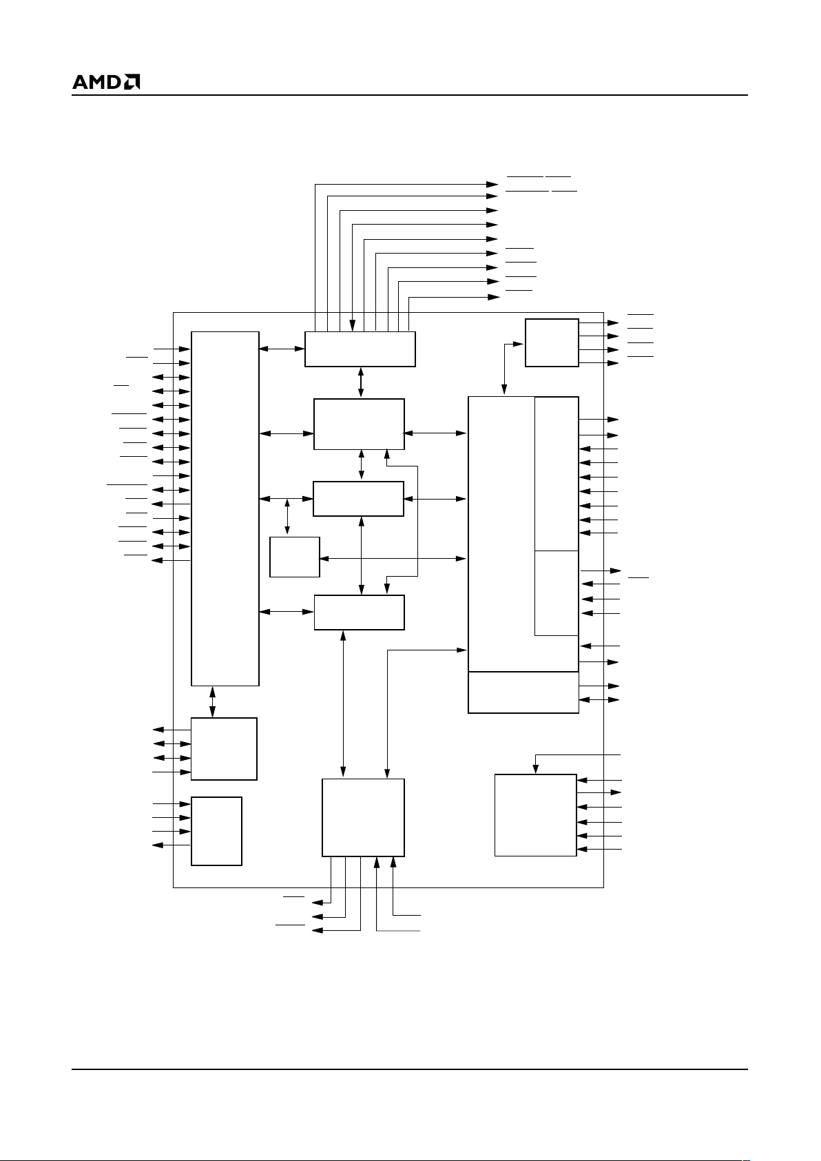
BLOCK DIAGRAM
CLK
RST
AD[31:0]
C/BE[3:0]
PAR
FRAME
TRDY
IRDY
STOP
IDSEL
DEVSEL
REQ
GNT
PERR
SERR
INTA
PCI Bus
Interface
Unit
93CXX
EEPROM
Interface
Expansion Bus
Interface
MIB
Counters
JTAG
Port
Control
OnNow
Power
Management
Unit
802.3
MAC
Core
MII
Port
EADI
Port
ERADV/FLOE
ERADSP/ICEN
ERCLK
ERD[31:0]/FLD[7:0]/FLA[23.20]
ERA[19:0]/FLA[19:0]
ERCE
EROE
ERWE
FLCS
PME
RWU
WUMI
PG
PHY_RST
TXD[3:0]
TX_EN
TX_CLK
COL
RXD[3:0]
RX_ER
RX_CLK
RX_DV
CRS
SFBD
EAR
RXFRTGD
RXFRTGE
EECS
EESK
EEDI
EEDO
LED0
LED1
LED2
LED3
Network Port
Manager
MDC
MDIO
Memory Control
Unit
Register Control
and Status Unit
Descriptor
Management Unit
LED
Control
VAUX_SENSE
Clock
Generator
XTAL1
XTAL2
XCLK
CLKSEL0
CLKSEL1
CLKSEL2
FC
TCK
TMS
TDI
TDO
TEST
22929B1
Page 5

8/01/00 Am79C976 5
PRELIMINARY
DISTINCTIVE CHARACTERISTICS . . . . . . . . . . . . . . . . . . . . . . . . . . . . . . . . . . . . . . . . . . . . . . . . . . . . . .1
GENERAL DESCRIPTION . . . . . . . . . . . . . . . . . . . . . . . . . . . . . . . . . . . . . . . . . . . . . . . . . . . . . . . . . . . . .3
BLOCK DIAGRAM. . . . . . . . . . . . . . . . . . . . . . . . . . . . . . . . . . . . . . . . . . . . . . . . . . . . . . . . . . . . . . . . . . . . 4
TABLE OF CONTENTS. . . . . . . . . . . . . . . . . . . . . . . . . . . . . . . . . . . . . . . . . . . . . . . . . . . . . . . . . . . . . . . . 5
LIST OF FIGURES. . . . . . . . . . . . . . . . . . . . . . . . . . . . . . . . . . . . . . . . . . . . . . . . . . . . . . . . . . . . . . . . . . .12
LIST OF TABLES . . . . . . . . . . . . . . . . . . . . . . . . . . . . . . . . . . . . . . . . . . . . . . . . . . . . . . . . . . . . . . . . . . . 14
ORDERING INFORMATION . . . . . . . . . . . . . . . . . . . . . . . . . . . . . . . . . . . . . . . . . . . . . . . . . . . . . . . . . . .17
Standard Products . . . . . . . . . . . . . . . . . . . . . . . . . . . . . . . . . . . . . . . . . . . . . . . . . . . . . . . . . . . . . . . . 17
CONNECTION DIAGRAM (PQR208) . . . . . . . . . . . . . . . . . . . . . . . . . . . . . . . . . . . . . . . . . . . . . . . . . . . .18
PIN DESIGNATIONS (PQR208) . . . . . . . . . . . . . . . . . . . . . . . . . . . . . . . . . . . . . . . . . . . . . . . . . . . . . . . . 19
Listed By Pin Number . . . . . . . . . . . . . . . . . . . . . . . . . . . . . . . . . . . . . . . . . . . . . . . . . . . . . . . . . . . . . 19
Listed By Group. . . . . . . . . . . . . . . . . . . . . . . . . . . . . . . . . . . . . . . . . . . . . . . . . . . . . . . . . . . . . . . . . . 21
PIN DESCRIPTIONS . . . . . . . . . . . . . . . . . . . . . . . . . . . . . . . . . . . . . . . . . . . . . . . . . . . . . . . . . . . . . . . . .24
PCI Interface . . . . . . . . . . . . . . . . . . . . . . . . . . . . . . . . . . . . . . . . . . . . . . . . . . . . . . . . . . . . . . . . . . . .24
Board Interface . . . . . . . . . . . . . . . . . . . . . . . . . . . . . . . . . . . . . . . . . . . . . . . . . . . . . . . . . . . . . . . . . . 26
EEPROM Interface . . . . . . . . . . . . . . . . . . . . . . . . . . . . . . . . . . . . . . . . . . . . . . . . . . . . . . . . . . . . . . . 28
External Memory Interface. . . . . . . . . . . . . . . . . . . . . . . . . . . . . . . . . . . . . . . . . . . . . . . . . . . . . . . . . . 28
Media Independent Interface. . . . . . . . . . . . . . . . . . . . . . . . . . . . . . . . . . . . . . . . . . . . . . . . . . . . . . . . 29
External Address Detection Interface . . . . . . . . . . . . . . . . . . . . . . . . . . . . . . . . . . . . . . . . . . . . . . . . .30
IEEE 1149.1 (1990) Test Access Port Interface. . . . . . . . . . . . . . . . . . . . . . . . . . . . . . . . . . . . . . . . . .31
Power Supply Pins. . . . . . . . . . . . . . . . . . . . . . . . . . . . . . . . . . . . . . . . . . . . . . . . . . . . . . . . . . . . . . . . 31
BASIC FUNCTIONS . . . . . . . . . . . . . . . . . . . . . . . . . . . . . . . . . . . . . . . . . . . . . . . . . . . . . . . . . . . . . . . . .32
System Bus Interface. . . . . . . . . . . . . . . . . . . . . . . . . . . . . . . . . . . . . . . . . . . . . . . . . . . . . . . . . . . . . . 32
Software Interface . . . . . . . . . . . . . . . . . . . . . . . . . . . . . . . . . . . . . . . . . . . . . . . . . . . . . . . . . . . . . . . . 32
Network Interface. . . . . . . . . . . . . . . . . . . . . . . . . . . . . . . . . . . . . . . . . . . . . . . . . . . . . . . . . . . . . . . . . 32
DETAILED FUNCTIONS . . . . . . . . . . . . . . . . . . . . . . . . . . . . . . . . . . . . . . . . . . . . . . . . . . . . . . . . . . . . . . 33
Slave Bus Interface Unit. . . . . . . . . . . . . . . . . . . . . . . . . . . . . . . . . . . . . . . . . . . . . . . . . . . . . . . . . . . .33
Slave Configuration Transfers . . . . . . . . . . . . . . . . . . . . . . . . . . . . . . . . . . . . . . . . . . . . . . . . . . . . . . . 33
Slave I/O Transfers. . . . . . . . . . . . . . . . . . . . . . . . . . . . . . . . . . . . . . . . . . . . . . . . . . . . . . . . . . . . . . . .33
Expansion ROM Transfers. . . . . . . . . . . . . . . . . . . . . . . . . . . . . . . . . . . . . . . . . . . . . . . . . . . . . . .37
Slave Cycle Termination . . . . . . . . . . . . . . . . . . . . . . . . . . . . . . . . . . . . . . . . . . . . . . . . . . . . . . . . 37
Disconnect When Busy. . . . . . . . . . . . . . . . . . . . . . . . . . . . . . . . . . . . . . . . . . . . . . . . . . . . . .37
Disconnect Of Burst T ransfer . . . . . . . . . . . . . . . . . . . . . . . . . . . . . . . . . . . . . . . . . . . . . . . . .38
Parity Error Response. . . . . . . . . . . . . . . . . . . . . . . . . . . . . . . . . . . . . . . . . . . . . . . . . . . . . . . . . .39
Master Bus Interface Unit . . . . . . . . . . . . . . . . . . . . . . . . . . . . . . . . . . . . . . . . . . . . . . . . . . . . . . . . . . 40
Bus Acquisition . . . . . . . . . . . . . . . . . . . . . . . . . . . . . . . . . . . . . . . . . . . . . . . . . . . . . . . . . . . . . . .40
Bus Master DMA Transfers . . . . . . . . . . . . . . . . . . . . . . . . . . . . . . . . . . . . . . . . . . . . . . . . . . . . . .40
Basic Non-Burst Read Transfer. . . . . . . . . . . . . . . . . . . . . . . . . . . . . . . . . . . . . . . . . . . . . . . .40
Basic Burst Read Transfer . . . . . . . . . . . . . . . . . . . . . . . . . . . . . . . . . . . . . . . . . . . . . . . . . . .41
Basic Non-Burst Write Transfer. . . . . . . . . . . . . . . . . . . . . . . . . . . . . . . . . . . . . . . . . . . . . . . . 42
Basic Burst Write Transfer . . . . . . . . . . . . . . . . . . . . . . . . . . . . . . . . . . . . . . . . . . . . . . . . . . .44
DMA Burst Alignment . . . . . . . . . . . . . . . . . . . . . . . . . . . . . . . . . . . . . . . . . . . . . . . . . . . . . . . . . .45
Target Initiated Termination . . . . . . . . . . . . . . . . . . . . . . . . . . . . . . . . . . . . . . . . . . . . . . . . . . . . . . 45
Disconnect With Data Transfer . . . . . . . . . . . . . . . . . . . . . . . . . . . . . . . . . . . . . . . . . . . . . . . .45
Disconnect Without Data Transfer. . . . . . . . . . . . . . . . . . . . . . . . . . . . . . . . . . . . . . . . . . . . . .46
Target Abort . . . . . . . . . . . . . . . . . . . . . . . . . . . . . . . . . . . . . . . . . . . . . . . . . . . . . . . . . . . . . .47
Master Initiated Termination . . . . . . . . . . . . . . . . . . . . . . . . . . . . . . . . . . . . . . . . . . . . . . . . . . . . . 48
Preemption During Non-Burst Transaction . . . . . . . . . . . . . . . . . . . . . . . . . . . . . . . . . . . . . . .48
Preemption During Burst Transaction. . . . . . . . . . . . . . . . . . . . . . . . . . . . . . . . . . . . . . . . . . .48
Master Abort . . . . . . . . . . . . . . . . . . . . . . . . . . . . . . . . . . . . . . . . . . . . . . . . . . . . . . . . . . . . . . . . .49
Parity Error Response. . . . . . . . . . . . . . . . . . . . . . . . . . . . . . . . . . . . . . . . . . . . . . . . . . . . . . . . . .51
Initialization Block DMA Transfers . . . . . . . . . . . . . . . . . . . . . . . . . . . . . . . . . . . . . . . . . . . . . . . . .52
Descriptor DMA Transfers . . . . . . . . . . . . . . . . . . . . . . . . . . . . . . . . . . . . . . . . . . . . . . . . . . . . . . . 52
FIFO DMA Transfers . . . . . . . . . . . . . . . . . . . . . . . . . . . . . . . . . . . . . . . . . . . . . . . . . . . . . . . . . . .57
Descriptor Management Unit. . . . . . . . . . . . . . . . . . . . . . . . . . . . . . . . . . . . . . . . . . . . . . . . . . . . . . . . 59
Initialization . . . . . . . . . . . . . . . . . . . . . . . . . . . . . . . . . . . . . . . . . . . . . . . . . . . . . . . . . . . . . . . . . .59
TABLE OF CONTENTS
Page 6

6 Am79C976 8/01/00
PRELIMINARY
Re-Initialization . . . . . . . . . . . . . . . . . . . . . . . . . . . . . . . . . . . . . . . . . . . . . . . . . . . . . . . . . . . . . . .60
Run and Suspend . . . . . . . . . . . . . . . . . . . . . . . . . . . . . . . . . . . . . . . . . . . . . . . . . . . . . . . . . . . . .60
Descriptor Management . . . . . . . . . . . . . . . . . . . . . . . . . . . . . . . . . . . . . . . . . . . . . . . . . . . . . . . . 61
Descriptor Rings . . . . . . . . . . . . . . . . . . . . . . . . . . . . . . . . . . . . . . . . . . . . . . . . . . . . . . . . . . . . . .61
Polling . . . . . . . . . . . . . . . . . . . . . . . . . . . . . . . . . . . . . . . . . . . . . . . . . . . . . . . . . . . . . . . . . . . . . .63
Transmit Polling . . . . . . . . . . . . . . . . . . . . . . . . . . . . . . . . . . . . . . . . . . . . . . . . . . . . . . . . . . . . . . .64
Receive Polling . . . . . . . . . . . . . . . . . . . . . . . . . . . . . . . . . . . . . . . . . . . . . . . . . . . . . . . . . . . . . . .65
Look Ahead Packet Processing . . . . . . . . . . . . . . . . . . . . . . . . . . . . . . . . . . . . . . . . . . . . . . . 65
Software Interrupt Timer . . . . . . . . . . . . . . . . . . . . . . . . . . . . . . . . . . . . . . . . . . . . . . . . . . . . . . . . . . .66
Media Access Control . . . . . . . . . . . . . . . . . . . . . . . . . . . . . . . . . . . . . . . . . . . . . . . . . . . . . . . . . . . . . 66
Transmit and Receive Message Data Encapsulation . . . . . . . . . . . . . . . . . . . . . . . . . . . . . . . . . . 66
Framing. . . . . . . . . . . . . . . . . . . . . . . . . . . . . . . . . . . . . . . . . . . . . . . . . . . . . . . . . . . . . . . . . . 66
Destination Address Handling. . . . . . . . . . . . . . . . . . . . . . . . . . . . . . . . . . . . . . . . . . . . . . . . . . . .67
Error Detection . . . . . . . . . . . . . . . . . . . . . . . . . . . . . . . . . . . . . . . . . . . . . . . . . . . . . . . . . . . . 67
Media Access Management . . . . . . . . . . . . . . . . . . . . . . . . . . . . . . . . . . . . . . . . . . . . . . . . . . . . .67
Medium Allocation. . . . . . . . . . . . . . . . . . . . . . . . . . . . . . . . . . . . . . . . . . . . . . . . . . . . . . . . . . 67
Signal Quality Error (SQE) Test . . . . . . . . . . . . . . . . . . . . . . . . . . . . . . . . . . . . . . . . . . . . . . .68
Collision Handling . . . . . . . . . . . . . . . . . . . . . . . . . . . . . . . . . . . . . . . . . . . . . . . . . . . . . . . . . .68
Transmit Operation. . . . . . . . . . . . . . . . . . . . . . . . . . . . . . . . . . . . . . . . . . . . . . . . . . . . . . . . . . . . . . . . 69
Transmit Function Programming . . . . . . . . . . . . . . . . . . . . . . . . . . . . . . . . . . . . . . . . . . . . . . . . . .69
Automatic Pad Generation . . . . . . . . . . . . . . . . . . . . . . . . . . . . . . . . . . . . . . . . . . . . . . . . . . . . . .69
Transmit FCS Generation . . . . . . . . . . . . . . . . . . . . . . . . . . . . . . . . . . . . . . . . . . . . . . . . . . . . . . . 70
Transmit Error Conditions . . . . . . . . . . . . . . . . . . . . . . . . . . . . . . . . . . . . . . . . . . . . . . . . . . . . . . .70
Loss of Carrier . . . . . . . . . . . . . . . . . . . . . . . . . . . . . . . . . . . . . . . . . . . . . . . . . . . . . . . . . . . . 71
Late Collision . . . . . . . . . . . . . . . . . . . . . . . . . . . . . . . . . . . . . . . . . . . . . . . . . . . . . . . . . . . . . 71
Transmit FIFO Underflow . . . . . . . . . . . . . . . . . . . . . . . . . . . . . . . . . . . . . . . . . . . . . . . . . . . .71
Receive Operation. . . . . . . . . . . . . . . . . . . . . . . . . . . . . . . . . . . . . . . . . . . . . . . . . . . . . . . . . . . . . . . .71
Receive Function Programming . . . . . . . . . . . . . . . . . . . . . . . . . . . . . . . . . . . . . . . . . . . . . . . . . .71
Address Matching . . . . . . . . . . . . . . . . . . . . . . . . . . . . . . . . . . . . . . . . . . . . . . . . . . . . . . . . . . . . .71
Automatic Pad Stripping . . . . . . . . . . . . . . . . . . . . . . . . . . . . . . . . . . . . . . . . . . . . . . . . . . . . . . . .72
Receive FCS Checking . . . . . . . . . . . . . . . . . . . . . . . . . . . . . . . . . . . . . . . . . . . . . . . . . . . . . . . . . 73
Receive Exception Conditions. . . . . . . . . . . . . . . . . . . . . . . . . . . . . . . . . . . . . . . . . . . . . . . . . . . .73
Statistics Counters. . . . . . . . . . . . . . . . . . . . . . . . . . . . . . . . . . . . . . . . . . . . . . . . . . . . . . . . . . . . . . . . 73
Receive Statistics Counters. . . . . . . . . . . . . . . . . . . . . . . . . . . . . . . . . . . . . . . . . . . . . . . . . . . . . .74
Transmit Statistics Counters . . . . . . . . . . . . . . . . . . . . . . . . . . . . . . . . . . . . . . . . . . . . . . . . . . . . .76
VLAN Support . . . . . . . . . . . . . . . . . . . . . . . . . . . . . . . . . . . . . . . . . . . . . . . . . . . . . . . . . . . . . . . . . . .78
VLAN Frame Size . . . . . . . . . . . . . . . . . . . . . . . . . . . . . . . . . . . . . . . . . . . . . . . . . . . . . . . . . . 79
Admit Only VLAN Frames Option . . . . . . . . . . . . . . . . . . . . . . . . . . . . . . . . . . . . . . . . . . . . . . 79
VLAN Tags in Descriptors. . . . . . . . . . . . . . . . . . . . . . . . . . . . . . . . . . . . . . . . . . . . . . . . . . . . 79
Loopback Operation. . . . . . . . . . . . . . . . . . . . . . . . . . . . . . . . . . . . . . . . . . . . . . . . . . . . . . . . . . . . . . . 80
Miscellaneous Loopback Features . . . . . . . . . . . . . . . . . . . . . . . . . . . . . . . . . . . . . . . . . . . . . . . .80
Full-Duplex Operation . . . . . . . . . . . . . . . . . . . . . . . . . . . . . . . . . . . . . . . . . . . . . . . . . . . . . . . . . . . . . 80
Full-Duplex Link Status LED Support . . . . . . . . . . . . . . . . . . . . . . . . . . . . . . . . . . . . . . . . . . . . . .81
Media Independent Interface. . . . . . . . . . . . . . . . . . . . . . . . . . . . . . . . . . . . . . . . . . . . . . . . . . . . . . . . 81
MII Transmit Interface . . . . . . . . . . . . . . . . . . . . . . . . . . . . . . . . . . . . . . . . . . . . . . . . . . . . . . . . . . 81
MII Receive Interface. . . . . . . . . . . . . . . . . . . . . . . . . . . . . . . . . . . . . . . . . . . . . . . . . . . . . . . . . . .81
MII Network Status Interface. . . . . . . . . . . . . . . . . . . . . . . . . . . . . . . . . . . . . . . . . . . . . . . . . . . . .82
MII Management Interface. . . . . . . . . . . . . . . . . . . . . . . . . . . . . . . . . . . . . . . . . . . . . . . . . . . . . . .82
MII Management Frames . . . . . . . . . . . . . . . . . . . . . . . . . . . . . . . . . . . . . . . . . . . . . . . . . . . . . . .82
Host CPU Access to External PHY. . . . . . . . . . . . . . . . . . . . . . . . . . . . . . . . . . . . . . . . . . . . . . . . 83
Auto-Poll State Machine . . . . . . . . . . . . . . . . . . . . . . . . . . . . . . . . . . . . . . . . . . . . . . . . . . . . . . . .84
Network Port Manager . . . . . . . . . . . . . . . . . . . . . . . . . . . . . . . . . . . . . . . . . . . . . . . . . . . . . . . . .85
Auto-Negotiation . . . . . . . . . . . . . . . . . . . . . . . . . . . . . . . . . . . . . . . . . . . . . . . . . . . . . . . . . . . . . . . . . 85
Auto-Negotiation With Multiple PHY Devices . . . . . . . . . . . . . . . . . . . . . . . . . . . . . . . . . . . . . . . . 86
Operation Without MMI Management Interface. . . . . . . . . . . . . . . . . . . . . . . . . . . . . . . . . . . . . . .86
Regulating Network Traffic. . . . . . . . . . . . . . . . . . . . . . . . . . . . . . . . . . . . . . . . . . . . . . . . . . . . . . . . . .87
MAC Control Pause Frames . . . . . . . . . . . . . . . . . . . . . . . . . . . . . . . . . . . . . . . . . . . . . . . . . . . . .87
Back Pressure. . . . . . . . . . . . . . . . . . . . . . . . . . . . . . . . . . . . . . . . . . . . . . . . . . . . . . . . . . . . . . . .87
Page 7

8/01/00 Am79C976 7
PRELIMINARY
Enabling Traffic Regulation . . . . . . . . . . . . . . . . . . . . . . . . . . . . . . . . . . . . . . . . . . . . . . . . . . . . . .87
Hardware Control of Traffic Regulation . . . . . . . . . . . . . . . . . . . . . . . . . . . . . . . . . . . . . . . . . . . . .88
Software Control of Traffic Regulation. . . . . . . . . . . . . . . . . . . . . . . . . . . . . . . . . . . . . . . . . . . . . .88
Programming the Pause Length Register . . . . . . . . . . . . . . . . . . . . . . . . . . . . . . . . . . . . . . . . . . .89
PAUSE Frame Reception . . . . . . . . . . . . . . . . . . . . . . . . . . . . . . . . . . . . . . . . . . . . . . . . . . . . . . .89
Delayed Interrupts . . . . . . . . . . . . . . . . . . . . . . . . . . . . . . . . . . . . . . . . . . . . . . . . . . . . . . . . . . . . . . . . 89
External Address Detection Interface . . . . . . . . . . . . . . . . . . . . . . . . . . . . . . . . . . . . . . . . . . . . . . . . .90
External Address Detection Interface: Receive Frame Tagging . . . . . . . . . . . . . . . . . . . . . . . . . .91
External Memory Interface. . . . . . . . . . . . . . . . . . . . . . . . . . . . . . . . . . . . . . . . . . . . . . . . . . . . . . . . . . 91
Expansion ROM - Boot Device Access . . . . . . . . . . . . . . . . . . . . . . . . . . . . . . . . . . . . . . . . . . . . .92
Direct Flash Access. . . . . . . . . . . . . . . . . . . . . . . . . . . . . . . . . . . . . . . . . . . . . . . . . . . . . . . . . . . .94
Flash/EPROM Read . . . . . . . . . . . . . . . . . . . . . . . . . . . . . . . . . . . . . . . . . . . . . . . . . . . . . . . . 94
SRAM Configuration . . . . . . . . . . . . . . . . . . . . . . . . . . . . . . . . . . . . . . . . . . . . . . . . . . . . . . . . . . .95
EEPROM Interface . . . . . . . . . . . . . . . . . . . . . . . . . . . . . . . . . . . . . . . . . . . . . . . . . . . . . . . . . . . . . . . 96
Automatic EEPROM Read Operation . . . . . . . . . . . . . . . . . . . . . . . . . . . . . . . . . . . . . . . . . . . . . .96
EEPROM Auto-Detection . . . . . . . . . . . . . . . . . . . . . . . . . . . . . . . . . . . . . . . . . . . . . . . . . . . . 98
Direct Access to the Interface. . . . . . . . . . . . . . . . . . . . . . . . . . . . . . . . . . . . . . . . . . . . . . . . .98
EEPROM CRC Calculation. . . . . . . . . . . . . . . . . . . . . . . . . . . . . . . . . . . . . . . . . . . . . . . . . . .98
LED Support . . . . . . . . . . . . . . . . . . . . . . . . . . . . . . . . . . . . . . . . . . . . . . . . . . . . . . . . . . . . . . . . . . . .98
Power Savings Mode . . . . . . . . . . . . . . . . . . . . . . . . . . . . . . . . . . . . . . . . . . . . . . . . . . . . . . . . . . . . . .99
Power Management Support. . . . . . . . . . . . . . . . . . . . . . . . . . . . . . . . . . . . . . . . . . . . . . . . . . . . .99
OnNow Wake-Up Sequence. . . . . . . . . . . . . . . . . . . . . . . . . . . . . . . . . . . . . . . . . . . . . . . . .100
RWU Wake-Up Sequence . . . . . . . . . . . . . . . . . . . . . . . . . . . . . . . . . . . . . . . . . . . . . . . . . .101
Link Change Detect . . . . . . . . . . . . . . . . . . . . . . . . . . . . . . . . . . . . . . . . . . . . . . . . . . . . . . .101
Magic Packet Mode. . . . . . . . . . . . . . . . . . . . . . . . . . . . . . . . . . . . . . . . . . . . . . . . . . . . . . . .101
OnNow Pattern Match Mode. . . . . . . . . . . . . . . . . . . . . . . . . . . . . . . . . . . . . . . . . . . . . . . . .102
Pattern Match RAM (PMR) . . . . . . . . . . . . . . . . . . . . . . . . . . . . . . . . . . . . . . . . . . . . . . . . . .102
IEEE 1149.1 (1990) Test Access Port Interface. . . . . . . . . . . . . . . . . . . . . . . . . . . . . . . . . . . . . . . . .103
Boundary Scan Circuit . . . . . . . . . . . . . . . . . . . . . . . . . . . . . . . . . . . . . . . . . . . . . . . . . . . . . . . .103
TAP Finite State Machine . . . . . . . . . . . . . . . . . . . . . . . . . . . . . . . . . . . . . . . . . . . . . . . . . . . . . . 103
Supported Instructions . . . . . . . . . . . . . . . . . . . . . . . . . . . . . . . . . . . . . . . . . . . . . . . . . . . . . . . . 103
Boundary Scan Register . . . . . . . . . . . . . . . . . . . . . . . . . . . . . . . . . . . . . . . . . . . . . . . . . . . . . . .104
Other Data Registers. . . . . . . . . . . . . . . . . . . . . . . . . . . . . . . . . . . . . . . . . . . . . . . . . . . . . . . . . .104
Reset . . . . . . . . . . . . . . . . . . . . . . . . . . . . . . . . . . . . . . . . . . . . . . . . . . . . . . . . . . . . . . . . . . . . . . . . . 104
H_RESET . . . . . . . . . . . . . . . . . . . . . . . . . . . . . . . . . . . . . . . . . . . . . . . . . . . . . . . . . . . . . . . . . .104
EE_RESET . . . . . . . . . . . . . . . . . . . . . . . . . . . . . . . . . . . . . . . . . . . . . . . . . . . . . . . . . . . . . . . . .104
S_RESET . . . . . . . . . . . . . . . . . . . . . . . . . . . . . . . . . . . . . . . . . . . . . . . . . . . . . . . . . . . . . . . . . .105
STOP. . . . . . . . . . . . . . . . . . . . . . . . . . . . . . . . . . . . . . . . . . . . . . . . . . . . . . . . . . . . . . . . . . . . . .105
Power on Reset. . . . . . . . . . . . . . . . . . . . . . . . . . . . . . . . . . . . . . . . . . . . . . . . . . . . . . . . . . . . . .105
External PHY Reset . . . . . . . . . . . . . . . . . . . . . . . . . . . . . . . . . . . . . . . . . . . . . . . . . . . . . . . . . .105
Software Access . . . . . . . . . . . . . . . . . . . . . . . . . . . . . . . . . . . . . . . . . . . . . . . . . . . . . . . . . . . . . . . . 106
PCI Configuration Registers . . . . . . . . . . . . . . . . . . . . . . . . . . . . . . . . . . . . . . . . . . . . . . . . . . . .106
I/O Resources . . . . . . . . . . . . . . . . . . . . . . . . . . . . . . . . . . . . . . . . . . . . . . . . . . . . . . . . . . . . . . .106
I/O Registers. . . . . . . . . . . . . . . . . . . . . . . . . . . . . . . . . . . . . . . . . . . . . . . . . . . . . . . . . . . . . 107
Address PROM Space . . . . . . . . . . . . . . . . . . . . . . . . . . . . . . . . . . . . . . . . . . . . . . . . . . . . . 107
Reset Register . . . . . . . . . . . . . . . . . . . . . . . . . . . . . . . . . . . . . . . . . . . . . . . . . . . . . . . . . . .107
Word I/O Mode . . . . . . . . . . . . . . . . . . . . . . . . . . . . . . . . . . . . . . . . . . . . . . . . . . . . . . . . . . . 108
Double Word I/O Mode . . . . . . . . . . . . . . . . . . . . . . . . . . . . . . . . . . . . . . . . . . . . . . . . . . . . .108
USER ACCESSIBLE REGISTERS . . . . . . . . . . . . . . . . . . . . . . . . . . . . . . . . . . . . . . . . . . . . . . . . . . . . .111
PCI Configuration Registers . . . . . . . . . . . . . . . . . . . . . . . . . . . . . . . . . . . . . . . . . . . . . . . . . . . . . . .111
PCI Vendor ID Register. . . . . . . . . . . . . . . . . . . . . . . . . . . . . . . . . . . . . . . . . . . . . . . . . . . . . . . .111
PCI Device ID Register . . . . . . . . . . . . . . . . . . . . . . . . . . . . . . . . . . . . . . . . . . . . . . . . . . . . . . . .111
PCI Command Register . . . . . . . . . . . . . . . . . . . . . . . . . . . . . . . . . . . . . . . . . . . . . . . . . . . . . . .111
PCI Status Register. . . . . . . . . . . . . . . . . . . . . . . . . . . . . . . . . . . . . . . . . . . . . . . . . . . . . . . . . . .113
PCI Revision ID Register. . . . . . . . . . . . . . . . . . . . . . . . . . . . . . . . . . . . . . . . . . . . . . . . . . . . . . .114
PCI Programming Interface Register. . . . . . . . . . . . . . . . . . . . . . . . . . . . . . . . . . . . . . . . . . . . . .114
PCI Sub-Class Register . . . . . . . . . . . . . . . . . . . . . . . . . . . . . . . . . . . . . . . . . . . . . . . . . . . . . . .114
PCI Base-Class Register. . . . . . . . . . . . . . . . . . . . . . . . . . . . . . . . . . . . . . . . . . . . . . . . . . . . . . .114
Page 8

8 Am79C976 8/01/00
PRELIMINARY
PCI Cache Line Size Register. . . . . . . . . . . . . . . . . . . . . . . . . . . . . . . . . . . . . . . . . . . . . . . . . . .115
PCI Latency Timer Register . . . . . . . . . . . . . . . . . . . . . . . . . . . . . . . . . . . . . . . . . . . . . . . . . . . .115
PCI Header Type Register. . . . . . . . . . . . . . . . . . . . . . . . . . . . . . . . . . . . . . . . . . . . . . . . . . . . . . 115
PCI I/O Base Address Register. . . . . . . . . . . . . . . . . . . . . . . . . . . . . . . . . . . . . . . . . . . . . . . . . .115
PCI Memory Mapped I/O Base Address Register. . . . . . . . . . . . . . . . . . . . . . . . . . . . . . . . . . . .116
PCI Subsystem Vendor ID Register . . . . . . . . . . . . . . . . . . . . . . . . . . . . . . . . . . . . . . . . . . . . . .116
PCI Subsystem ID Register. . . . . . . . . . . . . . . . . . . . . . . . . . . . . . . . . . . . . . . . . . . . . . . . . . . . .117
PCI Expansion ROM Base Address Register . . . . . . . . . . . . . . . . . . . . . . . . . . . . . . . . . . . . . . .117
PCI Capabilities Pointer Register . . . . . . . . . . . . . . . . . . . . . . . . . . . . . . . . . . . . . . . . . . . . . . . .118
PCI Interrupt Line Register . . . . . . . . . . . . . . . . . . . . . . . . . . . . . . . . . . . . . . . . . . . . . . . . . . . . .118
PCI Interrupt Pin Register . . . . . . . . . . . . . . . . . . . . . . . . . . . . . . . . . . . . . . . . . . . . . . . . . . . . . . 118
PCI MIN_GNT Register. . . . . . . . . . . . . . . . . . . . . . . . . . . . . . . . . . . . . . . . . . . . . . . . . . . . . . . . 118
PCI MAX_LAT Register. . . . . . . . . . . . . . . . . . . . . . . . . . . . . . . . . . . . . . . . . . . . . . . . . . . . . . . . 119
PCI Capability Identifier Register . . . . . . . . . . . . . . . . . . . . . . . . . . . . . . . . . . . . . . . . . . . . . . . .119
PCI Next Item Pointer Register . . . . . . . . . . . . . . . . . . . . . . . . . . . . . . . . . . . . . . . . . . . . . . . . . . 119
PCI Power Management Capabilities Register (PMC) . . . . . . . . . . . . . . . . . . . . . . . . . . . . . . . .119
PCI Power Management Control/Status Register (PMCSR). . . . . . . . . . . . . . . . . . . . . . . . . . . .120
PCI PMCSR Bridge Support Extensions Register . . . . . . . . . . . . . . . . . . . . . . . . . . . . . . . . . . .121
PCI Data Register . . . . . . . . . . . . . . . . . . . . . . . . . . . . . . . . . . . . . . . . . . . . . . . . . . . . . . . . . . . .121
Memory-Mapped Registers . . . . . . . . . . . . . . . . . . . . . . . . . . . . . . . . . . . . . . . . . . . . . . . . . . . . . . . . 122
MIB Offset . . . . . . . . . . . . . . . . . . . . . . . . . . . . . . . . . . . . . . . . . . . . . . . . . . . . . . . . . . . . . . . . . .122
AP_VALUE0: Auto-Poll Value0 Register . . . . . . . . . . . . . . . . . . . . . . . . . . . . . . . . . . . . . . . . . . .122
AP_VALUE1: Auto-Poll Value1 Register . . . . . . . . . . . . . . . . . . . . . . . . . . . . . . . . . . . . . . . . . . .122
AP_VALUE2: Auto-Poll Value2 Register . . . . . . . . . . . . . . . . . . . . . . . . . . . . . . . . . . . . . . . . . . .123
AP_VALUE3: Auto-Poll Value3 Register . . . . . . . . . . . . . . . . . . . . . . . . . . . . . . . . . . . . . . . . . . .123
AP_VALUE4: Auto-Poll Value4 Register . . . . . . . . . . . . . . . . . . . . . . . . . . . . . . . . . . . . . . . . . . .123
AP_VALUE5: Auto-Poll Value5 Register . . . . . . . . . . . . . . . . . . . . . . . . . . . . . . . . . . . . . . . . . . .123
AUTOPOLL0: Auto-Poll0 Register. . . . . . . . . . . . . . . . . . . . . . . . . . . . . . . . . . . . . . . . . . . . . . . . 123
AUTOPOLL1: Auto-Poll1 Register. . . . . . . . . . . . . . . . . . . . . . . . . . . . . . . . . . . . . . . . . . . . . . . . 124
AUTOPOLL2: Auto-Poll2 Register. . . . . . . . . . . . . . . . . . . . . . . . . . . . . . . . . . . . . . . . . . . . . . . . 125
AUTOPOLL3: Auto-Poll3 Register. . . . . . . . . . . . . . . . . . . . . . . . . . . . . . . . . . . . . . . . . . . . . . . . 126
AUTOPOLL4: Auto-Poll4 Register. . . . . . . . . . . . . . . . . . . . . . . . . . . . . . . . . . . . . . . . . . . . . . . . 127
AUTOPOLL5: Auto-Poll5 Register. . . . . . . . . . . . . . . . . . . . . . . . . . . . . . . . . . . . . . . . . . . . . . . . 128
BADR: Receive Ring Base Address Register . . . . . . . . . . . . . . . . . . . . . . . . . . . . . . . . . . . . . . .128
BADX: Transmit Ring Base Address Register. . . . . . . . . . . . . . . . . . . . . . . . . . . . . . . . . . . . . . .129
CHIPID: Chip ID Register . . . . . . . . . . . . . . . . . . . . . . . . . . . . . . . . . . . . . . . . . . . . . . . . . . . . . .129
CHPOLLTIME: Chain Poll Timer Register. . . . . . . . . . . . . . . . . . . . . . . . . . . . . . . . . . . . . . . . . .129
CMD0: Command0 . . . . . . . . . . . . . . . . . . . . . . . . . . . . . . . . . . . . . . . . . . . . . . . . . . . . . . . . . . .130
CMD2: Command2 . . . . . . . . . . . . . . . . . . . . . . . . . . . . . . . . . . . . . . . . . . . . . . . . . . . . . . . . . . .131
CMD3: Command3 . . . . . . . . . . . . . . . . . . . . . . . . . . . . . . . . . . . . . . . . . . . . . . . . . . . . . . . . . . .135
CMD7: Command7 . . . . . . . . . . . . . . . . . . . . . . . . . . . . . . . . . . . . . . . . . . . . . . . . . . . . . . . . . . .138
CTRL0: Control0 Register. . . . . . . . . . . . . . . . . . . . . . . . . . . . . . . . . . . . . . . . . . . . . . . . . . . . . .139
CTRL1: Control1 Register. . . . . . . . . . . . . . . . . . . . . . . . . . . . . . . . . . . . . . . . . . . . . . . . . . . . . .140
CTRL2: Control2 Register. . . . . . . . . . . . . . . . . . . . . . . . . . . . . . . . . . . . . . . . . . . . . . . . . . . . . .143
CTRL3: Control3 Register. . . . . . . . . . . . . . . . . . . . . . . . . . . . . . . . . . . . . . . . . . . . . . . . . . . . . .144
DATAMBIST: Memory Built-in Self-Test Access Register . . . . . . . . . . . . . . . . . . . . . . . . . . . . . .145
DELAYED_INT: Delayed Interrupts Register. . . . . . . . . . . . . . . . . . . . . . . . . . . . . . . . . . . . . . . .147
EEPROM_ACC: EEPROM Access Register. . . . . . . . . . . . . . . . . . . . . . . . . . . . . . . . . . . . . . . . 147
FLASH_ADDR: Flash Address Register . . . . . . . . . . . . . . . . . . . . . . . . . . . . . . . . . . . . . . . . . . . 150
FLASH_DATA: Flash Data Register . . . . . . . . . . . . . . . . . . . . . . . . . . . . . . . . . . . . . . . . . . . . . .150
FLOW: Flow Control Register. . . . . . . . . . . . . . . . . . . . . . . . . . . . . . . . . . . . . . . . . . . . . . . . . . .151
IFS1: Inter-Frame Spacing Part 1 Register . . . . . . . . . . . . . . . . . . . . . . . . . . . . . . . . . . . . . . . . .152
INT0: Interrupt0 . . . . . . . . . . . . . . . . . . . . . . . . . . . . . . . . . . . . . . . . . . . . . . . . . . . . . . . . . . . . . . 153
INTEN0: Interrupt0 Enable . . . . . . . . . . . . . . . . . . . . . . . . . . . . . . . . . . . . . . . . . . . . . . . . . . . . .155
IPG: Inter-Packet Gap Register. . . . . . . . . . . . . . . . . . . . . . . . . . . . . . . . . . . . . . . . . . . . . . . . . .157
LADRF: Logical Address Filter Register . . . . . . . . . . . . . . . . . . . . . . . . . . . . . . . . . . . . . . . . . . .157
LED0 Control Register . . . . . . . . . . . . . . . . . . . . . . . . . . . . . . . . . . . . . . . . . . . . . . . . . . . . . . . .158
LED1 Control Register . . . . . . . . . . . . . . . . . . . . . . . . . . . . . . . . . . . . . . . . . . . . . . . . . . . . . . . .159
Page 9

8/01/00 Am79C976 9
PRELIMINARY
LED2 Control Register . . . . . . . . . . . . . . . . . . . . . . . . . . . . . . . . . . . . . . . . . . . . . . . . . . . . . . . .159
LED3 Control Register . . . . . . . . . . . . . . . . . . . . . . . . . . . . . . . . . . . . . . . . . . . . . . . . . . . . . . . .159
MAX_LAT_A: PCI Maximum Latency Alias Register. . . . . . . . . . . . . . . . . . . . . . . . . . . . . . . . . .160
MIN_GNT_A: PCI Minimum Grant Alias Register. . . . . . . . . . . . . . . . . . . . . . . . . . . . . . . . . . . .160
PADR: Physical Address Register. . . . . . . . . . . . . . . . . . . . . . . . . . . . . . . . . . . . . . . . . . . . . . . .160
Pause Count Register . . . . . . . . . . . . . . . . . . . . . . . . . . . . . . . . . . . . . . . . . . . . . . . . . . . . . . . . . 161
PCIDATA0: PCI DATA Register Zero Alias Register . . . . . . . . . . . . . . . . . . . . . . . . . . . . . . . . . .161
PCIDATA1: PCI DATA Register One Alias Register. . . . . . . . . . . . . . . . . . . . . . . . . . . . . . . . . . .161
PCIDATA2: PCI DATA Register Two Alias Register . . . . . . . . . . . . . . . . . . . . . . . . . . . . . . . . . . .162
PCIDATA3: PCI DATA Register Three Alias Register . . . . . . . . . . . . . . . . . . . . . . . . . . . . . . . . .162
PCIDATA4: PCI DATA Register Four Alias Register . . . . . . . . . . . . . . . . . . . . . . . . . . . . . . . . . . 162
PCIDATA5: PCI DATA Register Five Alias Register. . . . . . . . . . . . . . . . . . . . . . . . . . . . . . . . . . . 162
PCIDATA6: PCI DATA Register Six Alias Register. . . . . . . . . . . . . . . . . . . . . . . . . . . . . . . . . . . .162
PCIDATA7: PCI DATA Register Seven Alias Register . . . . . . . . . . . . . . . . . . . . . . . . . . . . . . . . . 162
PHY Access Register. . . . . . . . . . . . . . . . . . . . . . . . . . . . . . . . . . . . . . . . . . . . . . . . . . . . . . . . .163
PMAT0: OnNow Pattern Register 0. . . . . . . . . . . . . . . . . . . . . . . . . . . . . . . . . . . . . . . . . . . . . . .164
PMAT1: OnNow Pattern Register 1. . . . . . . . . . . . . . . . . . . . . . . . . . . . . . . . . . . . . . . . . . . . . . .164
PMC_A: PCI Power Management Capabilities Alias Register . . . . . . . . . . . . . . . . . . . . . . . . . . 165
Receive Protect Register. . . . . . . . . . . . . . . . . . . . . . . . . . . . . . . . . . . . . . . . . . . . . . . . . . . . . . .165
RCV_RING_LEN: Receive Ring Length Register. . . . . . . . . . . . . . . . . . . . . . . . . . . . . . . . . . . . 165
ROM_CFG: ROM Base Address Configuration Register . . . . . . . . . . . . . . . . . . . . . . . . . . . . . .166
SID_A: PCI Subsystem ID Alias Register . . . . . . . . . . . . . . . . . . . . . . . . . . . . . . . . . . . . . . . . . .166
SRAM Boundary Register . . . . . . . . . . . . . . . . . . . . . . . . . . . . . . . . . . . . . . . . . . . . . . . . . . . . .167
SRAM Size Register . . . . . . . . . . . . . . . . . . . . . . . . . . . . . . . . . . . . . . . . . . . . . . . . . . . . . . . . . .167
STAT0: Status0 . . . . . . . . . . . . . . . . . . . . . . . . . . . . . . . . . . . . . . . . . . . . . . . . . . . . . . . . . . . . . .168
Software Timer Value Register . . . . . . . . . . . . . . . . . . . . . . . . . . . . . . . . . . . . . . . . . . . . . . . . . .169
SVID_A: PCI Subsystem Vendor ID Alias Register. . . . . . . . . . . . . . . . . . . . . . . . . . . . . . . . . . .170
VID_A: PCI Vendor ID Alias Register . . . . . . . . . . . . . . . . . . . . . . . . . . . . . . . . . . . . . . . . . . . . .171
XMT_RING_LEN: Transmit Ring Length Register . . . . . . . . . . . . . . . . . . . . . . . . . . . . . . . . . . .171
XMTPOLLTIME: Transmit Poll Timer Register . . . . . . . . . . . . . . . . . . . . . . . . . . . . . . . . . . . . . . 171
RAP Register. . . . . . . . . . . . . . . . . . . . . . . . . . . . . . . . . . . . . . . . . . . . . . . . . . . . . . . . . . . . . . . . . . . 172
RAP: Register Address Port . . . . . . . . . . . . . . . . . . . . . . . . . . . . . . . . . . . . . . . . . . . . . . . . . . . .172
Control and Status Registers. . . . . . . . . . . . . . . . . . . . . . . . . . . . . . . . . . . . . . . . . . . . . . . . . . . . . . .173
CSR0: Am79C976 Controller Status and Control Register. . . . . . . . . . . . . . . . . . . . . . . . . . . . .173
CSR1: Initialization Block Address 0. . . . . . . . . . . . . . . . . . . . . . . . . . . . . . . . . . . . . . . . . . . . . .175
CSR2: Initialization Block Address 1. . . . . . . . . . . . . . . . . . . . . . . . . . . . . . . . . . . . . . . . . . . . . .175
CSR3: Interrupt Masks and Deferral Control. . . . . . . . . . . . . . . . . . . . . . . . . . . . . . . . . . . . . . . .175
CSR4: Test and Features Control . . . . . . . . . . . . . . . . . . . . . . . . . . . . . . . . . . . . . . . . . . . . . . . .177
CSR5: Extended Control and Interrupt 1. . . . . . . . . . . . . . . . . . . . . . . . . . . . . . . . . . . . . . . . . . .179
CSR6: Reserved . . . . . . . . . . . . . . . . . . . . . . . . . . . . . . . . . . . . . . . . . . . . . . . . . . . . . . . . . . . . .181
CSR7: Extended Control and Interrupt 2. . . . . . . . . . . . . . . . . . . . . . . . . . . . . . . . . . . . . . . . . . .181
CSR8: Logical Address Filter 0 . . . . . . . . . . . . . . . . . . . . . . . . . . . . . . . . . . . . . . . . . . . . . . . . . .184
CSR9: Logical Address Filter 1 . . . . . . . . . . . . . . . . . . . . . . . . . . . . . . . . . . . . . . . . . . . . . . . . . .184
CSR10: Logical Address Filter 2 . . . . . . . . . . . . . . . . . . . . . . . . . . . . . . . . . . . . . . . . . . . . . . . . .184
CSR11: Logical Address Filter 3 . . . . . . . . . . . . . . . . . . . . . . . . . . . . . . . . . . . . . . . . . . . . . . . . .184
CSR12: Physical Address Register 0 . . . . . . . . . . . . . . . . . . . . . . . . . . . . . . . . . . . . . . . . . . . . .184
CSR13: Physical Address Register 1 . . . . . . . . . . . . . . . . . . . . . . . . . . . . . . . . . . . . . . . . . . . . .185
CSR14: Physical Address Register 2 . . . . . . . . . . . . . . . . . . . . . . . . . . . . . . . . . . . . . . . . . . . . .185
CSR15: Mode . . . . . . . . . . . . . . . . . . . . . . . . . . . . . . . . . . . . . . . . . . . . . . . . . . . . . . . . . . . . . . .185
CSR16-23: Reserved . . . . . . . . . . . . . . . . . . . . . . . . . . . . . . . . . . . . . . . . . . . . . . . . . . . . . . . . .186
CSR24: Base Address of Receive Ring Lower . . . . . . . . . . . . . . . . . . . . . . . . . . . . . . . . . . . . . .187
CSR25: Base Address of Receive Ring Upper . . . . . . . . . . . . . . . . . . . . . . . . . . . . . . . . . . . . . .187
CSR26-29: Reserved . . . . . . . . . . . . . . . . . . . . . . . . . . . . . . . . . . . . . . . . . . . . . . . . . . . . . . . . .187
CSR30: Base Address of Transmit Ring Lower. . . . . . . . . . . . . . . . . . . . . . . . . . . . . . . . . . . . . .187
CSR31: Base Address of Transmit Ring Upper. . . . . . . . . . . . . . . . . . . . . . . . . . . . . . . . . . . . . .187
CSR32-46: Reserved . . . . . . . . . . . . . . . . . . . . . . . . . . . . . . . . . . . . . . . . . . . . . . . . . . . . . . . . .188
CSR47: Transmit Polling Interval. . . . . . . . . . . . . . . . . . . . . . . . . . . . . . . . . . . . . . . . . . . . . . . . .188
CSR48: Reserved . . . . . . . . . . . . . . . . . . . . . . . . . . . . . . . . . . . . . . . . . . . . . . . . . . . . . . . . . . . .188
Page 10

10 Am79C976 8/01/00
PRELIMINARY
CSR49: Chain Polling Interval. . . . . . . . . . . . . . . . . . . . . . . . . . . . . . . . . . . . . . . . . . . . . . . . . . .188
CSR50-57: Reserved . . . . . . . . . . . . . . . . . . . . . . . . . . . . . . . . . . . . . . . . . . . . . . . . . . . . . . . . .189
CSR58: Software Style . . . . . . . . . . . . . . . . . . . . . . . . . . . . . . . . . . . . . . . . . . . . . . . . . . . . . . . .189
CSR59-75: Reserved . . . . . . . . . . . . . . . . . . . . . . . . . . . . . . . . . . . . . . . . . . . . . . . . . . . . . . . . .191
CSR76: Receive Ring Length . . . . . . . . . . . . . . . . . . . . . . . . . . . . . . . . . . . . . . . . . . . . . . . . . . .191
CSR77: Reserved . . . . . . . . . . . . . . . . . . . . . . . . . . . . . . . . . . . . . . . . . . . . . . . . . . . . . . . . . . . .191
CSR78: Transmit Ring Length. . . . . . . . . . . . . . . . . . . . . . . . . . . . . . . . . . . . . . . . . . . . . . . . . . .191
CSR79: Reserved . . . . . . . . . . . . . . . . . . . . . . . . . . . . . . . . . . . . . . . . . . . . . . . . . . . . . . . . . . . .191
CSR80: DMA Transfer Counter and FIFO Threshold Control . . . . . . . . . . . . . . . . . . . . . . . . . . .191
CSR81-87: Reserved . . . . . . . . . . . . . . . . . . . . . . . . . . . . . . . . . . . . . . . . . . . . . . . . . . . . . . . . .193
CSR88: Chip ID Register Lower . . . . . . . . . . . . . . . . . . . . . . . . . . . . . . . . . . . . . . . . . . . . . . . . .193
CSR89: Chip ID Register Upper . . . . . . . . . . . . . . . . . . . . . . . . . . . . . . . . . . . . . . . . . . . . . . . . .193
CSR90-99: Reserved . . . . . . . . . . . . . . . . . . . . . . . . . . . . . . . . . . . . . . . . . . . . . . . . . . . . . . . . .193
CSR100: Bus Timeout. . . . . . . . . . . . . . . . . . . . . . . . . . . . . . . . . . . . . . . . . . . . . . . . . . . . . . . . .193
CSR101-111: Reserved . . . . . . . . . . . . . . . . . . . . . . . . . . . . . . . . . . . . . . . . . . . . . . . . . . . . . . . 193
CSR112: Missed Frame Count . . . . . . . . . . . . . . . . . . . . . . . . . . . . . . . . . . . . . . . . . . . . . . . . . .193
CSR113: Reserved . . . . . . . . . . . . . . . . . . . . . . . . . . . . . . . . . . . . . . . . . . . . . . . . . . . . . . . . . . .193
CSR114: Receive Collision Count. . . . . . . . . . . . . . . . . . . . . . . . . . . . . . . . . . . . . . . . . . . . . . . .193
CSR115: Reserved . . . . . . . . . . . . . . . . . . . . . . . . . . . . . . . . . . . . . . . . . . . . . . . . . . . . . . . . . . .193
CSR116: OnNow Power Mode Register . . . . . . . . . . . . . . . . . . . . . . . . . . . . . . . . . . . . . . . . . . .194
CSR117-121: Reserved . . . . . . . . . . . . . . . . . . . . . . . . . . . . . . . . . . . . . . . . . . . . . . . . . . . . . . . 195
CSR122: Advanced Feature Control. . . . . . . . . . . . . . . . . . . . . . . . . . . . . . . . . . . . . . . . . . . . . .195
CSR123: Reserved . . . . . . . . . . . . . . . . . . . . . . . . . . . . . . . . . . . . . . . . . . . . . . . . . . . . . . . . . . .195
CSR124: Test Register 1. . . . . . . . . . . . . . . . . . . . . . . . . . . . . . . . . . . . . . . . . . . . . . . . . . . . . . . 195
CSR125: MAC Enhanced Configuration Control. . . . . . . . . . . . . . . . . . . . . . . . . . . . . . . . . . . . .196
Bus Configuration Registers . . . . . . . . . . . . . . . . . . . . . . . . . . . . . . . . . . . . . . . . . . . . . . . . . . . . . . . 197
BCR0: Master Mode Read Active . . . . . . . . . . . . . . . . . . . . . . . . . . . . . . . . . . . . . . . . . . . . . . . .198
BCR1: Master Mode Write Active . . . . . . . . . . . . . . . . . . . . . . . . . . . . . . . . . . . . . . . . . . . . . . . .198
BCR2: Miscellaneous Configuration . . . . . . . . . . . . . . . . . . . . . . . . . . . . . . . . . . . . . . . . . . . . . .199
BCR4: LED0 Status. . . . . . . . . . . . . . . . . . . . . . . . . . . . . . . . . . . . . . . . . . . . . . . . . . . . . . . . . . .199
BCR5: LED1 Status. . . . . . . . . . . . . . . . . . . . . . . . . . . . . . . . . . . . . . . . . . . . . . . . . . . . . . . . . . .201
BCR6: LED2 Status. . . . . . . . . . . . . . . . . . . . . . . . . . . . . . . . . . . . . . . . . . . . . . . . . . . . . . . . . . .203
BCR7: LED3 Status. . . . . . . . . . . . . . . . . . . . . . . . . . . . . . . . . . . . . . . . . . . . . . . . . . . . . . . . . . .205
BCR9: Full-Duplex Control . . . . . . . . . . . . . . . . . . . . . . . . . . . . . . . . . . . . . . . . . . . . . . . . . . . . .207
BCR16: I/O Base Address Lower . . . . . . . . . . . . . . . . . . . . . . . . . . . . . . . . . . . . . . . . . . . . . . . .207
BCR17: I/O Base Address Upper . . . . . . . . . . . . . . . . . . . . . . . . . . . . . . . . . . . . . . . . . . . . . . . .208
BCR18: Burst and Bus Control Register . . . . . . . . . . . . . . . . . . . . . . . . . . . . . . . . . . . . . . . . . . .208
BCR19: EEPROM Control and Status . . . . . . . . . . . . . . . . . . . . . . . . . . . . . . . . . . . . . . . . . . . .209
BCR20: Software Style . . . . . . . . . . . . . . . . . . . . . . . . . . . . . . . . . . . . . . . . . . . . . . . . . . . . . . . .212
BCR22: PCI Latency Register. . . . . . . . . . . . . . . . . . . . . . . . . . . . . . . . . . . . . . . . . . . . . . . . . . .214
BCR23: PCI Subsystem Vendor ID Register. . . . . . . . . . . . . . . . . . . . . . . . . . . . . . . . . . . . . . . . 214
BCR24: PCI Subsystem ID Register. . . . . . . . . . . . . . . . . . . . . . . . . . . . . . . . . . . . . . . . . . . . . .215
BCR25: SRAM Size Register . . . . . . . . . . . . . . . . . . . . . . . . . . . . . . . . . . . . . . . . . . . . . . . . . . .215
BCR26: SRAM Boundary Register . . . . . . . . . . . . . . . . . . . . . . . . . . . . . . . . . . . . . . . . . . . . . . .215
BCR27: SRAM Interface Control Register. . . . . . . . . . . . . . . . . . . . . . . . . . . . . . . . . . . . . . . . . .216
BCR28: Expansion Bus Port Address Lower (Used for Flash/EPROM and SRAM Accesses). . 216
BCR29: Expansion Port Address Upper (Used for Flash/EPROM Accesses) . . . . . . . . . . . . . . 216
BCR30: Expansion Bus Data Port Register . . . . . . . . . . . . . . . . . . . . . . . . . . . . . . . . . . . . . . . .217
BCR31: Software Timer Register . . . . . . . . . . . . . . . . . . . . . . . . . . . . . . . . . . . . . . . . . . . . . . . .217
BCR32: MII Control and Status Register. . . . . . . . . . . . . . . . . . . . . . . . . . . . . . . . . . . . . . . . . . .217
BCR33: MII Address Register. . . . . . . . . . . . . . . . . . . . . . . . . . . . . . . . . . . . . . . . . . . . . . . . . . .219
BCR34: MII Management Data Register. . . . . . . . . . . . . . . . . . . . . . . . . . . . . . . . . . . . . . . . . . .220
BCR35: PCI Vendor ID Register . . . . . . . . . . . . . . . . . . . . . . . . . . . . . . . . . . . . . . . . . . . . . . . . . 220
BCR36: PCI Power Management Capabilities (PMC) Alias Register . . . . . . . . . . . . . . . . . . . . .220
BCR37: PCI DAT A Register Zero (DATA0) Alias Register . . . . . . . . . . . . . . . . . . . . . . . . . . . . . .221
BCR38: PCI DATA Register One (DATA1) Alias Register . . . . . . . . . . . . . . . . . . . . . . . . . . . . . . 221
BCR39: PCI DATA Register Two (DATA2) Alias Register . . . . . . . . . . . . . . . . . . . . . . . . . . . . . .221
BCR40: PCI DATA Register Three (DATA3) Alias Register . . . . . . . . . . . . . . . . . . . . . . . . . . . . .222
Page 11

8/01/00 Am79C976 11
PRELIMINARY
BCR41: PCI DATA Register Four (DATA4) Alias Register . . . . . . . . . . . . . . . . . . . . . . . . . . . . . .222
BCR42: PCI DAT A Register Five (DATA5) Alias Register . . . . . . . . . . . . . . . . . . . . . . . . . . . . . . 222
BCR43: PCI DAT A Register Six (DATA6) Alias Register . . . . . . . . . . . . . . . . . . . . . . . . . . . . . . .223
BCR44: PCI DATA Register Seven (DATA7) Alias Register. . . . . . . . . . . . . . . . . . . . . . . . . . . . . 223
BCR45: OnNow Pattern Matching Register 1 . . . . . . . . . . . . . . . . . . . . . . . . . . . . . . . . . . . . . . .223
BCR46: OnNow Pattern Matching Register 2 . . . . . . . . . . . . . . . . . . . . . . . . . . . . . . . . . . . . . . .224
BCR47: OnNow Pattern Matching Register 3 . . . . . . . . . . . . . . . . . . . . . . . . . . . . . . . . . . . . . . .224
Initialization Block . . . . . . . . . . . . . . . . . . . . . . . . . . . . . . . . . . . . . . . . . . . . . . . . . . . . . . . . . . . . . . .225
RLEN and TLEN . . . . . . . . . . . . . . . . . . . . . . . . . . . . . . . . . . . . . . . . . . . . . . . . . . . . . . . . . . . . .225
RDRA and TDRA . . . . . . . . . . . . . . . . . . . . . . . . . . . . . . . . . . . . . . . . . . . . . . . . . . . . . . . . . . . . 226
LADRF. . . . . . . . . . . . . . . . . . . . . . . . . . . . . . . . . . . . . . . . . . . . . . . . . . . . . . . . . . . . . . . . . . . . .226
PADR. . . . . . . . . . . . . . . . . . . . . . . . . . . . . . . . . . . . . . . . . . . . . . . . . . . . . . . . . . . . . . . . . . . . . .226
Mode . . . . . . . . . . . . . . . . . . . . . . . . . . . . . . . . . . . . . . . . . . . . . . . . . . . . . . . . . . . . . . . . . . . . . .226
Receive Descriptors. . . . . . . . . . . . . . . . . . . . . . . . . . . . . . . . . . . . . . . . . . . . . . . . . . . . . . . . . . . . . . 227
Transmit Descriptors . . . . . . . . . . . . . . . . . . . . . . . . . . . . . . . . . . . . . . . . . . . . . . . . . . . . . . . . . . . . .238
REGISTER SUMMARY . . . . . . . . . . . . . . . . . . . . . . . . . . . . . . . . . . . . . . . . . . . . . . . . . . . . . . . . . . . . . .245
PCI Configuration Registers . . . . . . . . . . . . . . . . . . . . . . . . . . . . . . . . . . . . . . . . . . . . . . . . . . . . . . .245
Memory-Mapped Registers . . . . . . . . . . . . . . . . . . . . . . . . . . . . . . . . . . . . . . . . . . . . . . . . . . . . . . . . 246
Control and Status Registers. . . . . . . . . . . . . . . . . . . . . . . . . . . . . . . . . . . . . . . . . . . . . . . . . . . . . . .248
Bus Configuration Registers . . . . . . . . . . . . . . . . . . . . . . . . . . . . . . . . . . . . . . . . . . . . . . . . . . . . . . . 252
REGISTER BIT CROSS REFERENCE . . . . . . . . . . . . . . . . . . . . . . . . . . . . . . . . . . . . . . . . . . . . . . . . . .253
REGISTER PROGRAMMING SUMMARY . . . . . . . . . . . . . . . . . . . . . . . . . . . . . . . . . . . . . . . . . . . . . . .262
Programmable Registers . . . . . . . . . . . . . . . . . . . . . . . . . . . . . . . . . . . . . . . . . . . . . . . . . . . . . . . . . . 262
ABSOLUTE MAXIMUM RATINGS . . . . . . . . . . . . . . . . . . . . . . . . . . . . . . . . . . . . . . . . . . . . . . . . . . . . .266
OPERATING RANGES . . . . . . . . . . . . . . . . . . . . . . . . . . . . . . . . . . . . . . . . . . . . . . . . . . . . . . . . . . . . . .266
DC CHARACTERISTICS OVER COMMERCIAL OPERATING RANGES . . . . . . . . . . . . . . . . . . . . . . . 267
SWITCHING CHARACTERISTICS: BUS INTERFACE . . . . . . . . . . . . . . . . . . . . . . . . . . . . . . . . . . . . .269
SWITCHING WAVEFORMS . . . . . . . . . . . . . . . . . . . . . . . . . . . . . . . . . . . . . . . . . . . . . . . . . . . . . . . . . .270
Key to Switching Waveforms . . . . . . . . . . . . . . . . . . . . . . . . . . . . . . . . . . . . . . . . . . . . . . . . . . . . . . .270
SWITCHING TEST CIRCUITS. . . . . . . . . . . . . . . . . . . . . . . . . . . . . . . . . . . . . . . . . . . . . . . . . . . . . . . . .271
SWITCHING WAVEFORMS: SYSTEM BUS INTERFA CE . . . . . . . . . . . . . . . . . . . . . . . . . . . . . . . . . . .272
SWITCHING CHARACTERISTICS: EEPROM INTERFACE. . . . . . . . . . . . . . . . . . . . . . . . . . . . . . . . . .274
SWITCHING CHARACTERISTICS: JTAG TIMING. . . . . . . . . . . . . . . . . . . . . . . . . . . . . . . . . . . . . . . . .276
SWITCHING CHARACTERISTICS: MEDIA INDEPENDENT INTERFACE . . . . . . . . . . . . . . . . . . . . . . 278
SWITCHING CHARACTERISTICS: EXTERNAL ADDRESS DETECTION INTERFACE . . . . . . . . . . .281
SWITCHING WAVEFORMS: RECEIVE FRAME TAG. . . . . . . . . . . . . . . . . . . . . . . . . . . . . . . . . . . . . . . 283
SWITCHING WAVEFORMS: EXTERNAL MEMORY INTERFACE . . . . . . . . . . . . . . . . . . . . . . . . . . . . 284
PHYSICAL DIMENSIONS* . . . . . . . . . . . . . . . . . . . . . . . . . . . . . . . . . . . . . . . . . . . . . . . . . . . . . . . . . . .285
PQFP208. . . . . . . . . . . . . . . . . . . . . . . . . . . . . . . . . . . . . . . . . . . . . . . . . . . . . . . . . . . . . . . . . . . . . . 285
Plastic Quad Flat Pack Trimmed and Formed. . . . . . . . . . . . . . . . . . . . . . . . . . . . . . . . . . . . . . .285
APPENDIX A: LOOK-AHEAD PACKET PROCESSING. . . . . . . . . . . . . . . . . . . . . . . . . . . . . . . . . . . . . A-1
Introduction . . . . . . . . . . . . . . . . . . . . . . . . . . . . . . . . . . . . . . . . . . . . . . . . . . . . . . . . . . . . . . . . . . . . A-1
Outline of LAPP Flow. . . . . . . . . . . . . . . . . . . . . . . . . . . . . . . . . . . . . . . . . . . . . . . . . . . . . . . . . . . . . A-2
Setup. . . . . . . . . . . . . . . . . . . . . . . . . . . . . . . . . . . . . . . . . . . . . . . . . . . . . . . . . . . . . . . . . . . . . . A-2
Flow. . . . . . . . . . . . . . . . . . . . . . . . . . . . . . . . . . . . . . . . . . . . . . . . . . . . . . . . . . . . . . . . . . . . . . . A-2
LAPP Software Requirements . . . . . . . . . . . . . . . . . . . . . . . . . . . . . . . . . . . . . . . . . . . . . . . . . . . . . . A-5
LAPP Rules for Parsing Descriptors . . . . . . . . . . . . . . . . . . . . . . . . . . . . . . . . . . . . . . . . . . . . . . . . . A-5
Some Examples of LAPP Descriptor Interaction . . . . . . . . . . . . . . . . . . . . . . . . . . . . . . . . . . . . . . . . A-6
Buffer Size Tuning . . . . . . . . . . . . . . . . . . . . . . . . . . . . . . . . . . . . . . . . . . . . . . . . . . . . . . . . . . . . A-7
An Alternative LAPP Flow: Two-Interrupt Method . . . . . . . . . . . . . . . . . . . . . . . . . . . . . . . . . . . . A-8
APPENDIX B: MII MANAGEMENT REGISTERS . . . . . . . . . . . . . . . . . . . . . . . . . . . . . . . . . . . . . . . . . . B-1
Control Register (Register 0). . . . . . . . . . . . . . . . . . . . . . . . . . . . . . . . . . . . . . . . . . . . . . . . . . . . . . . B-1
Status Register (Register 1) . . . . . . . . . . . . . . . . . . . . . . . . . . . . . . . . . . . . . . . . . . . . . . . . . . . . . . . B-2
Auto-Negotiation Advertisement Register (Register 4) . . . . . . . . . . . . . . . . . . . . . . . . . . . . . . . . . . . B-3
Technology Ability Field Bit Assignments . . . . . . . . . . . . . . . . . . . . . . . . . . . . . . . . . . . . . . . . . . B-3
Auto-Negotiation Link Partner Ability Register (Register 5). . . . . . . . . . . . . . . . . . . . . . . . . . . . . . . . B-4
INDEX . . . . . . . . . . . . . . . . . . . . . . . . . . . . . . . . . . . . . . . . . . . . . . . . . . . . . . . . . . . . . . . . . . . . . . .INDEX-1
Page 12

12 Am79C976 7/25/00
PRELIMINARY
LIST OF FIGURES
Figure 1: Slave Configuration Read . . . . . . . . . . . . . . . . . . . . . . . . . . . . . . . . . . . . . 34
Figure 2: Slave Configuration Write . . . . . . . . . . . . . . . . . . . . . . . . . . . . . . . . . . . . . 34
Figure 3: Slave Read Using I/O Command . . . . . . . . . . . . . . . . . . . . . . . . . . . . . . . . 35
Figure 4: Slave Write Using Memory Command . . . . . . . . . . . . . . . . . . . . . . . . . . . . 36
Figure 5: Disconnect Of Slave Cycle When Busy . . . . . . . . . . . . . . . . . . . . . . . . . . . 38
Figure 6: Disconnect Of Slave Burst Transfer - No Host Wait States . . . . . . . . . . . . 38
Figure 7: Disconnect Of Slave Burst Transfer - Host Inserts Wait States . . . . . . . . . 39
Figure 8: Address Parity Error Response . . . . . . . . . . . . . . . . . . . . . . . . . . . . . . . . . 39
Figure 9: Slave Cycle Data Parity Error Response . . . . . . . . . . . . . . . . . . . . . . . . . . 40
Figure 10: Bus Acquisition . . . . . . . . . . . . . . . . . . . . . . . . . . . . . . . . . . . . . . . . . . . . . 41
Figure 11: Non-Burst Read Transfer . . . . . . . . . . . . . . . . . . . . . . . . . . . . . . . . . . . . . 42
Figure 12: Burst Read Transfer . . . . . . . . . . . . . . . . . . . . . . . . . . . . . . . . . . . . . . . . . 43
Figure 13: Non-Burst Write Transfer . . . . . . . . . . . . . . . . . . . . . . . . . . . . . . . . . . . . . . 44
Figure 14: Burst Write Transfer . . . . . . . . . . . . . . . . . . . . . . . . . . . . . . . . . . . . . . . . . . 45
Figure 15: Disconnect With Data Transfer . . . . . . . . . . . . . . . . . . . . . . . . . . . . . . . . . 46
Figure 16: Disconnect Without Data Transfer . . . . . . . . . . . . . . . . . . . . . . . . . . . . . . . 47
Figure 17: Target Abort . . . . . . . . . . . . . . . . . . . . . . . . . . . . . . . . . . . . . . . . . . . . . . . . 48
Figure 18: Preemption During Non-Burst Transaction . . . . . . . . . . . . . . . . . . . . . . . . 49
Figure 19: Preemption During Burst Transaction . . . . . . . . . . . . . . . . . . . . . . . . . . . . 50
Figure 20: Master Abor . . . . . . . . . . . . . . . . . . . . . . . . . . . . . . . . . . . . . . . . . . . . . . . . 51
Figure 21: Master Cycle Data Parity Error Response . . . . . . . . . . . . . . . . . . . . . . . . . 52
Figure 22: Descriptor Ring Read In Non-Burst Mode . . . . . . . . . . . . . . . . . . . . . . . . . 53
Figure 23: Descriptor Ring Read In Burst Mode . . . . . . . . . . . . . . . . . . . . . . . . . . . . . 54
Figure 24: Descriptor Ring Write In Non-Burst Mode . . . . . . . . . . . . . . . . . . . . . . . . . 56
Figure 25: Descriptor Ring Write In Burst Mode . . . . . . . . . . . . . . . . . . . . . . . . . . . . . 57
Figure 26: FIFO Burst Write At Start Of Unaligned Buffer . . . . . . . . . . . . . . . . . . . . . 58
Figure 27: FIFO Burst Write At End Of Unaligned Buffer . . . . . . . . . . . . . . . . . . . . . . 59
Figure 28: 16-Bit Software Model . . . . . . . . . . . . . . . . . . . . . . . . . . . . . . . . . . . . . . . . 62
Figure 29: 32-Bit Software Model . . . . . . . . . . . . . . . . . . . . . . . . . . . . . . . . . . . . . . . . 63
Figure 30: ISO 8802-3 (IEEE/ANSI 802.3) Data Frame . . . . . . . . . . . . . . . . . . . . . . . 70
Figure 31: IEEE 802.3 Frame and Length Field Transmission Order . . . . . . . . . . . . . 73
Figure 32: VLAN-Tagged Frame Format . . . . . . . . . . . . . . . . . . . . . . . . . . . . . . . . . . 79
Figure 33: Media Independent Interface . . . . . . . . . . . . . . . . . . . . . . . . . . . . . . . . . . . 82
Figure 34: Frame Format at the MII Interface Connection . . . . . . . . . . . . . . . . . . . . . 83
Figure 35: MII Receive Frame Tagging . . . . . . . . . . . . . . . . . . . . . . . . . . . . . . . . . . . . 91
Figure 36: External SSRAM and Flash Configuration . . . . . . . . . . . . . . . . . . . . . . . . . 92
Figure 37: Expansion ROM Bus Read Sequence . . . . . . . . . . . . . . . . . . . . . . . . . . . . 93
Figure 38: Flash Read from Expansion Bus Data Port . . . . . . . . . . . . . . . . . . . . . . . . 95
Figure 39: Flash Write Sequence . . . . . . . . . . . . . . . . . . . . . . . . . . . . . . . . . . . . . . . . 95
Figure 40: EEPROM Data Format . . . . . . . . . . . . . . . . . . . . . . . . . . . . . . . . . . . . . . . 97
Figure 41: EEPROM Entry Positions . . . . . . . . . . . . . . . . . . . . . . . . . . . . . . . . . . . . . 97
Figure 42: CRC Flow . . . . . . . . . . . . . . . . . . . . . . . . . . . . . . . . . . . . . . . . . . . . . . . . . . 98
Figure 43: LED Control Logic . . . . . . . . . . . . . . . . . . . . . . . . . . . . . . . . . . . . . . . . . . . 99
Figure 44: OnNow Functional Diagram . . . . . . . . . . . . . . . . . . . . . . . . . . . . . . . . . . . 100
Figure 45: Pattern Match RAM . . . . . . . . . . . . . . . . . . . . . . . . . . . . . . . . . . . . . . . . . 103
Figure 46: PCI Expansion ROM Base Address Register . . . . . . . . . . . . . . . . . . . . . 117
Figure 47: Address Match Logic . . . . . . . . . . . . . . . . . . . . . . . . . . . . . . . . . . . . . . . .2 27
Figure 48: Normal and Tri-State Outputs . . . . . . . . . . . . . . . . . . . . . . . . . . . . . . . . . 271
Page 13

7/25/00 Am79C976 13
PRELIMINARY
Figure 49: CLK Waveform for 5 V Signaling . . . . . . . . . . . . . . . . . . . . . . . . . . . . . . . 272
Figure 50: CLK Waveform for 3.3 V Signaling . . . . . . . . . . . . . . . . . . . . . . . . . . . . . 272
Figure 51: Input Setup and Hold Timing . . . . . . . . . . . . . . . . . . . . . . . . . . . . . . . . . . 272
Figure 52: Output Valid Delay Timing . . . . . . . . . . . . . . . . . . . . . . . . . . . . . . . . . . . . 273
Figure 53: Output Tri-State Delay Timing . . . . . . . . . . . . . . . . . . . . . . . . . . . . . . . . . 273
Figure 54: EEPROM Read Functional Timing . . . . . . . . . . . . . . . . . . . . . . . . . . . . . 274
Figure 55: Automatic PREAD EEPROM Timing . . . . . . . . . . . . . . . . . . . . . . . . . . . . 275
Figure 56: JTAG (IEEE 1149.1) TCK Waveform for 5 V Signaling . . . . . . . . . . . . . . 276
Figure 57: JTAG (IEEE 1149.1) Test Signal Timing . . . . . . . . . . . . . . . . . . . . . . . . . 277
Figure 58: Transmit Timing . . . . . . . . . . . . . . . . . . . . . . . . . . . . . . . . . . . . . . . . . . . . 279
Figure 59: Receive Timing . . . . . . . . . . . . . . . . . . . . . . . . . . . . . . . . . . . . . . . . . . . . 279
Figure 60: MDC Waveform . . . . . . . . . . . . . . . . . . . . . . . . . . . . . . . . . . . . . . . . . . . .279
Figure 61: Management Data Setup and Hold Timing . . . . . . . . . . . . . . . . . . . . . . .280
Figure 62: Management Data Output Valid Delay Timing . . . . . . . . . . . . . . . . . . . . . 280
Figure 63: Reject Timing - External PHY MII @ 25 MHz . . . . . . . . . . . . . . . . . . . . . 281
Figure 64: Reject Timing - External PHY MII @ 2.5 MHz . . . . . . . . . . . . . . . . . . . . . 282
Figure 65: Receive Frame Tag Timing with Media Independent Interface . . . . . . . .283
Figure 66: External Memory Timing . . . . . . . . . . . . . . . . . . . . . . . . . . . . . . . . . . . . . 284
Figure A-1: LAPP Timeline . . . . . . . . . . . . . . . . . . . . . . . . . . . . . . . . . . . . . . . . . . . . . A-4
Figure A-2: LAPP 3 Buffer Grouping . . . . . . . . . . . . . . . . . . . . . . . . . . . . . . . . . . . . . A-5
Figure A-3: LAPP Timeline for Two-Interrupt Method . . . . . . . . . . . . . . . . . . . . . . . . . A-9
Figure A-4: LAPP 3 Buffer Grouping for Two-Interrupt Method . . . . . . . . . . . . . . . . A-10
Page 14

14 Am79C976 7/25/00
PRELIMINARY
LIST OF TABLES
Table 1: System Clock Selections . . . . . . . . . . . . . . . . . . . . . . . . . . . . . . . . . . . . . . 27
Table 2: Slave Commands . . . . . . . . . . . . . . . . . . . . . . . . . . . . . . . . . . . . . . . . . . . . 33
Table 3: PCI Commands . . . . . . . . . . . . . . . . . . . . . . . . . . . . . . . . . . . . . . . . . . . . . 41
Table 4: Descriptor Read Sequence . . . . . . . . . . . . . . . . . . . . . . . . . . . . . . . . . . . . 54
Table 5: Descriptor Write Sequence . . . . . . . . . . . . . . . . . . . . . . . . . . . . . . . . . . . . . 55
Table 6: Receive Address Match . . . . . . . . . . . . . . . . . . . . . . . . . . . . . . . . . . . . . . . 72
Table 7: Receive Statistics Counters . . . . . . . . . . . . . . . . . . . . . . . . . . . . . . . . . . . . 74
Table 8: Transmit Statistics Counters . . . . . . . . . . . . . . . . . . . . . . . . . . . . . . . . . . . . 76
Table 9: VLAN Tag Control Command . . . . . . . . . . . . . . . . . . . . . . . . . . . . . . . . . . . 80
Table 10: VLAN Tag Type . . . . . . . . . . . . . . . . . . . . . . . . . . . . . . . . . . . . . . . . . . . . . 80
Table 11: Auto-Negotiation Capabilities . . . . . . . . . . . . . . . . . . . . . . . . . . . . . . . . . . . 85
Table 12: MAC Control Pause Frame Format . . . . . . . . . . . . . . . . . . . . . . . . . . . . . . 87
Table 13: FC Pin Functions . . . . . . . . . . . . . . . . . . . . . . . . . . . . . . . . . . . . . . . . . . . . 88
Table 14: FCCMD Bit Functions . . . . . . . . . . . . . . . . . . . . . . . . . . . . . . . . . . . . . . . . . 89
Table 15: SRAM_TYPE Field Encoding . . . . . . . . . . . . . . . . . . . . . . . . . . . . . . . . . . . 92
Table 16: LED Default Configuration . . . . . . . . . . . . . . . . . . . . . . . . . . . . . . . . . . . . . 99
Table 17: IEEE 1149.1 Supported Instruction Summary . . . . . . . . . . . . . . . . . . . . . 104
Table 18: BSR Mode Of Operation . . . . . . . . . . . . . . . . . . . . . . . . . . . . . . . . . . . . . . 104
Table 19: Device ID Register . . . . . . . . . . . . . . . . . . . . . . . . . . . . . . . . . . . . . . . . . . 104
Table 20: PCI Configuration Space Layout . . . . . . . . . . . . . . . . . . . . . . . . . . . . . . . 106
Table 21: Address PROM Space Contents . . . . . . . . . . . . . . . . . . . . . . . . . . . . . . . 107
Table 22: I/O Map In Word I/O Mode (DWIO = 0) . . . . . . . . . . . . . . . . . . . . . . . . . . 108
Table 23: Legal I/O Accesses in Word I/O Mode (DWIO = 0) . . . . . . . . . . . . . . . . . 109
Table 24: I/O Map In DWord I/O Mode (DWIO = 1) . . . . . . . . . . . . . . . . . . . . . . . . . 109
Table 25: Legal I/O Accesses in Double Word I/O Mode (DWIO =1) . . . . . . . . . . . . 109
Table 26: AP_VALUE0: Auto-Poll Value0 Register . . . . . . . . . . . . . . . . . . . . . . . . . 122
Table 27: AP_VALUE1: Auto-Poll Value1 Register . . . . . . . . . . . . . . . . . . . . . . . . . 123
Table 28: AP_VALUE2: Auto-Poll Value2 Register . . . . . . . . . . . . . . . . . . . . . . . . . 123
Table 29: AP_VALUE3: Auto-Poll Value3 Register . . . . . . . . . . . . . . . . . . . . . . . . . 123
Table 30: AP_VALUE4: Auto-Poll Value4 Register . . . . . . . . . . . . . . . . . . . . . . . . . 123
Table 31: AP_VALUE5: Auto-Poll Value5 Register . . . . . . . . . . . . . . . . . . . . . . . . . 123
Table 32: AUTOPOLL0: Auto-Poll0 Register . . . . . . . . . . . . . . . . . . . . . . . . . . . . . 123
Table 33: AUTOPOLL1: Auto-Poll1 Register . . . . . . . . . . . . . . . . . . . . . . . . . . . . . 124
Table 34: AUTOPOLL2: Auto-Poll2 Register . . . . . . . . . . . . . . . . . . . . . . . . . . . . . 125
Table 35: AUTOPOLL3: Auto-Poll3 Register . . . . . . . . . . . . . . . . . . . . . . . . . . . . . 126
Table 36: AUTOPOLL4: Auto-Poll4 Register . . . . . . . . . . . . . . . . . . . . . . . . . . . . . 127
Table 37: AUTOPOLL5: Auto-Poll5 Register . . . . . . . . . . . . . . . . . . . . . . . . . . . . . 128
Table 38: Receive Ring Base Address Register . . . . . . . . . . . . . . . . . . . . . . . . . . . 128
Table 39: Transmit Ring Base Address Register . . . . . . . . . . . . . . . . . . . . . . . . . . . 129
Table 40: CHIPID: Chip ID Register . . . . . . . . . . . . . . . . . . . . . . . . . . . . . . . . . . . . . 129
Table 41: CHPOLLTIME: Chain Polling Interval Register . . . . . . . . . . . . . . . . . . . . 129
Table 42: CMD0: Command0 Register . . . . . . . . . . . . . . . . . . . . . . . . . . . . . . . . . . 130
Table 43: CMD2: Command2 Register . . . . . . . . . . . . . . . . . . . . . . . . . . . . . . . . . . 131
Table 44: CMD3: Command3 Register . . . . . . . . . . . . . . . . . . . . . . . . . . . . . . . . . . 135
Table 45: CMD7: Command7 Register . . . . . . . . . . . . . . . . . . . . . . . . . . . . . . . . . . 138
Table 46: CTRL0: Control0 Register . . . . . . . . . . . . . . . . . . . . . . . . . . . . . . . . . . . . 139
Table 47: CTRL1: Control1 Register . . . . . . . . . . . . . . . . . . . . . . . . . . . . . . . . . . . . 140
Table 48: CTRL2: Control2 Register . . . . . . . . . . . . . . . . . . . . . . . . . . . . . . . . . . . . 143
Page 15

7/25/00 Am79C976 15
PRELIMINARY
Table 49: CTRL3: Control3 Register . . . . . . . . . . . . . . . . . . . . . . . . . . . . . . . . . . . . 144
Table 50: Software Styles . . . . . . . . . . . . . . . . . . . . . . . . . . . . . . . . . . . . . . . . . . . . . 144
Table 51: DATAMBIST: Memory Built-in Self-Test Access Register . . . . . . . . . . . . 145
Table 52: DELAYED_INT: Delayed Interrupts Register . . . . . . . . . . . . . . . . . . . . . . 147
Table 53: EEPROM_ACC: EEPROM Access Register . . . . . . . . . . . . . . . . . . . . . .148
Table 54: Interface Pin Assignment . . . . . . . . . . . . . . . . . . . . . . . . . . . . . . . . . . . . . 149
Table 55: FLASH_ADDR: Flash Address Register . . . . . . . . . . . . . . . . . . . . . . . . . 150
Table 56: FLASH_DATA: Flash Data Register . . . . . . . . . . . . . . . . . . . . . . . . . . . . . 150
Table 57: FLOW: Flow Control Register . . . . . . . . . . . . . . . . . . . . . . . . . . . . . . . . . 151
Table 58: IFS1: Inter-Frame Spacing Part 1 Register . . . . . . . . . . . . . . . . . . . . . . . 152
Table 59: INT0: Interrupt0 Register . . . . . . . . . . . . . . . . . . . . . . . . . . . . . . . . . . . . .153
Table 60: INTEN0: Interrupt0 Enable Register . . . . . . . . . . . . . . . . . . . . . . . . . . . . . 155
Table 61: IPG: Inter-Packet Gap Register . . . . . . . . . . . . . . . . . . . . . . . . . . . . . . . . 157
Table 62: Logical Address Filter Register . . . . . . . . . . . . . . . . . . . . . . . . . . . . . . . . . 157
Table 63: LED0 Control Register . . . . . . . . . . . . . . . . . . . . . . . . . . . . . . . . . . . . . . . 158
Table 64: MAX_LAT_A: PCI Maximum Latency Alias Register . . . . . . . . . . . . . . . . 160
Table 65: MIN_GNT_A: PCI Minimum Grant Alias Register . . . . . . . . . . . . . . . . . . 160
Table 66: PADR: Physical Address Register . . . . . . . . . . . . . . . . . . . . . . . . . . . . . . 161
Table 67: PAUSE_CNT: Pause Count Register . . . . . . . . . . . . . . . . . . . . . . . . . . . . 161
Table 68: PCIDATA0: PCI DATA Register Zero Alias Register . . . . . . . . . . . . . . . . 161
Table 69: PHY_ACCESS: PHY Access Register . . . . . . . . . . . . . . . . . . . . . . . . . . . 163
Table 70: PMAT0: OnNow Pattern Register 0 . . . . . . . . . . . . . . . . . . . . . . . . . . . . . 164
Table 71: PMAT1: OnNow Pattern Register 1 . . . . . . . . . . . . . . . . . . . . . . . . . . . . . 164
Table 72: Receive Protect Register . . . . . . . . . . . . . . . . . . . . . . . . . . . . . . . . . . . . .165
Table 73: RCV_RING_LEN: Receive Ring Length Register . . . . . . . . . . . . . . . . . . 165
Table 74: ROM_CFG: ROM Base Address Configuration Register . . . . . . . . . . . . .166
Table 75: SID_A: PCI Subsystem ID Alias Register . . . . . . . . . . . . . . . . . . . . . . . . . 166
Table 76: SRAM Boundary Register . . . . . . . . . . . . . . . . . . . . . . . . . . . . . . . . . . . . 167
Table 77: SRAM Size Register . . . . . . . . . . . . . . . . . . . . . . . . . . . . . . . . . . . . . . . . .167
Table 78: STAT0: Status0 Register . . . . . . . . . . . . . . . . . . . . . . . . . . . . . . . . . . . . .168
Table 79: Software Timer Value Register . . . . . . . . . . . . . . . . . . . . . . . . . . . . . . . . 169
Table 80: SVID: PCI Subsystem Vendor ID Shadow Register . . . . . . . . . . . . . . . . . 170
Table 81: TEST0: Test Register . . . . . . . . . . . . . . . . . . . . . . . . . . . . . . . . . . . . . . . .170
Table 82: VID_A: PCI Vendor ID Alias Register . . . . . . . . . . . . . . . . . . . . . . . . . . . . 171
Table 83: XMT_RING_LEN: Transmit Ring Length Register . . . . . . . . . . . . . . . . . . 171
Table 84: XMTPOLLTIME: Transmit Polling Interval Register . . . . . . . . . . . . . . . . . 172
Table 85: Software Styles . . . . . . . . . . . . . . . . . . . . . . . . . . . . . . . . . . . . . . . . . . . . . 190
Table 86: Receive Watermark Programming . . . . . . . . . . . . . . . . . . . . . . . . . . . . . . 192
Table 87: Transmit Start Point Programming . . . . . . . . . . . . . . . . . . . . . . . . . . . . . . 192
Table 88: Transmit Watermark Programming . . . . . . . . . . . . . . . . . . . . . . . . . . . . . 192
Table 89: BCR Registers . . . . . . . . . . . . . . . . . . . . . . . . . . . . . . . . . . . . . . . . . . . . . 197
Table 90: EEDET Setting . . . . . . . . . . . . . . . . . . . . . . . . . . . . . . . . . . . . . . . . . . . . . 211
Table 91: Interface Pin Assignment . . . . . . . . . . . . . . . . . . . . . . . . . . . . . . . . . . . . . 211
Table 92: Software Styles . . . . . . . . . . . . . . . . . . . . . . . . . . . . . . . . . . . . . . . . . . . . . 214
Table 93: SRAM_BND Programming . . . . . . . . . . . . . . . . . . . . . . . . . . . . . . . . . . . . 216
Table 94: FMDC Values . . . . . . . . . . . . . . . . . . . . . . . . . . . . . . . . . . . . . . . . . . . . . . 218
Table 95: APDW Values . . . . . . . . . . . . . . . . . . . . . . . . . . . . . . . . . . . . . . . . . . . . . . 218
Table 96: Initialization Block (SSIZE32 = 0) . . . . . . . . . . . . . . . . . . . . . . . . . . . . . . . 225
Table 97: Initialization Block (SSIZE32 = 1) . . . . . . . . . . . . . . . . . . . . . . . . . . . . . . . 225
Page 16

16 Am79C976 7/25/00
PRELIMINARY
Table 98: R/TLEN Decoding (SSIZE32 = 0) . . . . . . . . . . . . . . . . . . . . . . . . . . . . . . .226
Table 99: R/TLEN Decoding (SSIZE32 = 1) . . . . . . . . . . . . . . . . . . . . . . . . . . . . . . .226
Table 100: Receive Descriptor (SWSTYLE = 0) . . . . . . . . . . . . . . . . . . . . . . . . . . . . 227
Table 101: Receive Descriptor (SWSTYLE = 2) . . . . . . . . . . . . . . . . . . . . . . . . . . . . 227
Table 102: Receive Descriptor (SWSTYLE = 3) . . . . . . . . . . . . . . . . . . . . . . . . . . . . 228
Table 103: Receive Descriptor (SWSTYLE = 4) . . . . . . . . . . . . . . . . . . . . . . . . . . . . 228
Table 104: Receive Descriptor (SWSTYLE = 5) . . . . . . . . . . . . . . . . . . . . . . . . . . . . 228
Table 105: Receive Descriptor, SWSTYLE = 0 . . . . . . . . . . . . . . . . . . . . . . . . . . . . . 229
Table 106: Receive Descriptor, SWSTYLE = 2 . . . . . . . . . . . . . . . . . . . . . . . . . . . . . 230
Table 107: Receive Descriptor, SWSTYLE = 3 . . . . . . . . . . . . . . . . . . . . . . . . . . . . . 232
Table 108: Receive Descriptor, SWSTYLE = 4 . . . . . . . . . . . . . . . . . . . . . . . . . . . . . 233
Table 109: Receive Descriptor, SWSTYLE = 5 . . . . . . . . . . . . . . . . . . . . . . . . . . . . . 235
Table 110: Transmit Descriptor (SWSTYLE = 0) . . . . . . . . . . . . . . . . . . . . . . . . . . . . 238
Table 111: Transmit Descriptor (SWSTYLE = 2) . . . . . . . . . . . . . . . . . . . . . . . . . . . . 238
Table 112: Transmit Descriptor (SWSTYLE = 3) . . . . . . . . . . . . . . . . . . . . . . . . . . . . 238
Table 113: Transmit Descriptor (SWSTYLE = 4) . . . . . . . . . . . . . . . . . . . . . . . . . . . . 238
Table 114: Transmit Descriptor (SWSTYLE = 5) . . . . . . . . . . . . . . . . . . . . . . . . . . . . 239
Table 115: Transmit Descriptor, SWSTYLE = 0 . . . . . . . . . . . . . . . . . . . . . . . . . . . . . 239
Table 116: Transmit Descriptor, SWSTYLE = 2 . . . . . . . . . . . . . . . . . . . . . . . . . . . . . 240
Table 117: Transmit Descriptor, SWSTYLE = 3 . . . . . . . . . . . . . . . . . . . . . . . . . . . . . 241
Table 118: Transmit Descriptor, SWSTYLE = 4 . . . . . . . . . . . . . . . . . . . . . . . . . . . . . 242
Table 119: Transmit Descriptor, SWSTYLE = 5 . . . . . . . . . . . . . . . . . . . . . . . . . . . . . 243
Table 120: Register Bit Cross Reference . . . . . . . . . . . . . . . . . . . . . . . . . . . . . . . . . 253
Table 121: Control and Status Registers . . . . . . . . . . . . . . . . . . . . . . . . . . . . . . . . . . 262
Table 122: Bus Configuration Registers . . . . . . . . . . . . . . . . . . . . . . . . . . . . . . . . . . . 264
Table B-1: MII Management Register Set . . . . . . . . . . . . . . . . . . . . . . . . . . . . . . . . . B-1
Table B-2: MII Management Control Register (Register 0) . . . . . . . . . . . . . . . . . . . . B-1
Table B-3: MII Management Status Register (Register 1) . . . . . . . . . . . . . . . . . . . . . B-2
Table B-4: Auto-Negotiation Advertisement Register (Register 4) . . . . . . . . . . . . . . . B-3
Table B-5: Technology Ability Field Bit Assignments . . . . . . . . . . . . . . . . . . . . . . . . . B-3
Table B-6: Auto-Negotiation Link Partner Ability Re gister (Register 5)
- Base Page Format. . . . . . . . . . . . . . . . . . . . . . . . . . . . . . . . . . . . . . . . . B-4
Page 17
8/01/00 Am79C976 17
PRELIMINARY
ORDERING INFORMATION
Standard Products
AMD standard produc ts are av ailable in sev eral pac kages and operating r anges. T he order number (Valid Combination) is f ormed
by a combination of the elements below.
AM79C976
TEMPERATURE RANGE
C = Commercial (0 C to +70 C)
I = Industrial (–40 C to 85 C
SPEED OPTION
PACKAGE TYPE
Valid Combinations list configurations planned to be
supported in volume for this device. Consult the local
AMD sales office to confirm availability of specific
valid combinations and to check on newly released
combinations.
Valid Combinations
DEVICE NUMBER/DESCRIPTION
Not applicable
K = Plastic Quad Flat Pack (PQR208)
Am79C976
PCnet-Pro 10/100 Mb ps PCI Ethernet Controller
Valid Combinations
AM79C976
KC\WV,
KI\W
ALTERNATE PACKAGING OPTION
\W = Trimmed and formed in a tray
\W
C
K
Page 18
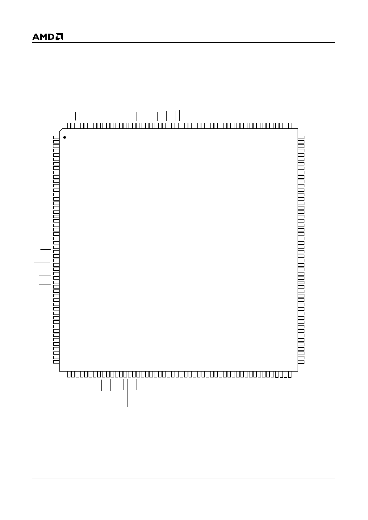
18 Am79C976 8/01/00
PRELIMINARY
CONNECTION DIAGRAM (PQR208)
200
199
198
197
196
195
194
193
192
191
190
189
188
187
186
185
184
183
182
181
180
179
178
177
176
175
174
173
171
170
169
168
167
166
165
164
163
162
161
172
156
155
154
153
152
151
150
149
148
147
146
145
144
143
142
141
140
139
138
137
136
135
134
133
132
131
130
129
127
126
125
124
123
122
121
120
119
118
117
128
6162636465666768697071727374757677787980818283848586878890919293949596979899100
89
1
2
3
4
5
6
7
8
9
10
11
12
13
14
15
16
17
18
19
20
21
22
23
24
25
26
27
28
30
31
32
33
34
35
36
37
38
39
40
29
ERD3/FLD3
ERD17
VDD
ERD18
ERD19
VSSB
TX_EN
TXD2
ERD0/FLD0
ERD1/FLD1
TXD1
TXD0
VSSB
CRS
VDD
ERD2/FLD2
VDD
ERD4/FLD4
ERD5/FLD5
ERD6/FLD6
VSS
ERD7/FLD7
VDD
ERD8/FLA20
ERD10/FLA22
ERD11/FLA23
VSSB
VDD
ERD13
ERD14
ERD15
ERD16
VSS
ERD12
ERD9/FLA21
VSSB
TXD3
COL
ERD20
VSSB
IRDY
VDD
TRDY
STOP
VSSB
PERR
VSS
SERR
PAR
VDD
C/BE1
AD15
AD14
AD30
AD29
VDD
AD28
AD27
AD26
VSSB
AD25
AD24
C/BE3
VDD
IDSEL
AD23
AD22
VSSB
AD21
AD20
AD19
VDD
AD18
AD17
AD16
VSSB
C/BE2
FRAME
DEVSEL
VSS
ERCE
VDD
EROE
VSSB
ERWE/FLWE
ERADV/FLOE
ERADSP/CEN
VSS
VSSB
ERA13/FLA13
ERA3/FLA3
ERA4/FLA4
VDD
ERA5/FLA5
ERA6/FLA6
ERA8/FLA8
ERA9/FLA9
VDD
VSS
VSSB
ERA11/FLA11
ERA12/FLA12
ERA14/FLA14
VDD
VSSB
ERA15/FLA15
VDD
ERA18/FLA18
ERA17/FLA17
VDD
FLCS
VSSB
ERA1/FLA1
ERA7/FLA7
ERA16/FLA16
ERD31
ERA0/FLA0
ERA10/FLA10
ERA2/FLA2
ERA19/FLA19
VDD
VSS
AVDD
VSSB
XTAL1
EAR
VDD
LED0/EEDI
LED2/RXFRTGE
XTAL2
LED3/EEDO/RXFRTGD
VSS
VSSB
CLKSEL0
TEST
VAUX_SENSE
PHY_RST
MDC
RXD3
VSSB
VDD
RXD0
EECS
PME
WUMI
FC
RWU
TCK
TMS
TDO
PG
VSSB
TDI
XCLK
CLKSEL1
MDIO
RXD2
RXD1
LED1/EESK
CLKSEL2
Am79C976
PCnet-PRO
INTA
RST
VDD
CLK
GNT
AD31
VSSB
REQ
41
42
43
44
45
46
47
48
VSSB
AD13
AD12
AD11
VDD
AD10
AD9
AD8
53545556575859
60
AD5
VDD
AD4
AD3
VSSB
AD2
AD1
AD0
116
115
114
113
112
111
110
109
VDD
ERD23
ERD24
ERD25
ERD22
ERD21
VSSB
ERCLK
49
50
51
52
VSSB
C/BE0
AD7
AD6
108
107
106
105
VSSB
ERD26
VDD
ERD27
101
102
103
104
ERD29
VSSB
ERD28
ERD30
160
159
158
157
RX_DV
RX_ER
TX_CLK
RX_CLK
208
207
206
205
204
203
202
201
22929B2
Page 19

8/01/00 Am79C976 19
PRELIMINARY
PIN DESIGNATIONS (PQR208)
Listed By Pin Number
Pin No. Pin Name Pin No. Pin Name Pin No. Pin Name Pin No. Pin Name
1 AD30 53 AD5 105 ERD27 157 TX_CLK
2 AD29 54 VDD 106 VDD 158 RX_ER
3 VDD 55 AD4 107 ERD26 159 RX_CLK
4 AD28 56 AD3 108 VSSB 160 RX_DV
5 AD27 57 VSSB 109 ERCLK 161 RXD0
6 AD26 58 AD2 110 ERD25 162 VDD
7 VSSB 59 AD1 111 ERD24 163 RXD1
8 AD25 60 AD0 112 ERD23 164 VSSB
9 AD24 61 ERCE 113 VDD 165 RXD2
10 C/BE3 62 VDD 114 ERD22 166 RXD3
11 VDD 63 EROE 115 VSSB 167 MDC
12 IDSEL 64 VSSB 116 ERD21 168 MDIO
13 AD23 65 ERWE/FLWE 117 ERD20 169 PHY_RST
14 AD22 66 ERADV/FLOE 118 ERD19 170 VAUX_SENSE
15 VSSB 67 ERADSP/CEN 119 ERD18 171 TEST
16 AD21 68 VSS 120 VDD 172 CLKSEL0
17 VSS 69 FLCS 121 ERD17 173 CLKSEL1
18 AD20 70 VDD 122 VSSB 174 VSSB
19 AD19 71 ERA0/FLA0 123 VSS 175 CLKSEL2
20 VDD 72 VSSB 124 ERD16 176 VSS
21 AD18 73 ERA1/FLA1 125 ERD15 177 XTAL2
22 AD17 74 ERA2/FLA2 126 ERD14 178 XTAL1
23 AD16 75 ERA3/FLA3 127 ERD13 179 AVDD
24 VSSB 76 ERA4/FLA4 128 VDD 180 XCLK
25 C/BE2 77 VDD 129 ERD12 181 VDD
26 FRAME
78 ERA5/FLA5 130 VSSB 182
LED3
/EEDO/
RXFRTGD
27 IRDY
79 VSSB 131 ERD11/FLA23 183 LED2/RXFRTGE
28 VDD 80 ERA6/FLA6 132 ERD10/FLA22 184 LED1/EESK
29 TRDY 81 ERA7/FLA7 133 ERD9/FLA21 185 LED0/EEDI
30 DEVSEL 82 ERA8/FLA8 134 ERD8/FLA20 186 EECS
31 STOP 83 ERA9/FLA9 135 VDD 187 EAR
32 VSSB 84 VDD 136 ERD7/FLD7 188 VSSB
33 PERR 85 ERA10/FLA10 137 VSSB 189 VSS
34 VSS 86 VSS 138 VSS 190 FC
Page 20

20 Am79C976 8/01/00
PRELIMINARY
35 SERR 87 VSSB 139 ERD6/FLD6 191 VDD
36 PAR 88 ERA11/FLA11 140 ERD5/FLD5 192 PME
37 VDD 89 ERA12/FLA12 141 ERD4/FLD4 193 WUMI
38 C/BE1 90 ERA13/FLA13 142 ERD3/FLD3 194 RWU
39 AD15 91 ERA14/FLA14 143 VDD 195 TCK
40 AD14 92 VDD 144 ERD2/FLD2 196 TMS
41 VSSB 93 ERA15/FLA15 145 VSSB 197 TDO
42 AD13 94 VSSB 146 ERD1/FLD1 198 TDI
43 AD12 95 ERA16/FLA16 147 ERD0/FLD0 199 VSSB
44 AD11 96 ERA17/FLA17 148 CRS 200 PG
45 VDD 97 ERA18/FLA18 149 COL 201 INTA
46 AD10 98 ERA19/FLA19 150 VDD 202 RST
47 AD9 99 VDD 151 TXD3 203 VDD
48 AD8 100 ERD31 152 TXD2 204 CLK
49 VSSB 101 VSSB 153 VSSB 205 GNT
50 C/BE0 102 ERD30 154 TXD1 206 REQ
51 AD7 103 ERD29 155 TXD0 207 VSSB
52 AD6 104 ERD28 156 TX_EN 208 AD31
Pin No. Pin Name Pin No. Pin Name Pin No. Pin Name Pin No. Pin Name
Page 21

8/01/00 Am79C976 21
PRELIMINARY
PIN DESIGNATIONS
Listed By Group
Pin Name Pin Function Signal Type1Pin Type1No. of Pins
Clock Interface
XTAL1 Crystal I I 1
XTAL2 Crystal O O 1
XCLK External Clock I I 1
CLKSEL0 Clock Select I I 1
CLKSEL1 Clock Select I I 1
CLKSEL2 Clock Select I I 1
TEST Test Select I I 1
PCI Bus Interface
AD[31:0] Address/Data Bus IO IO 32
C/BE[3:0] Bus Command/Byte Enable IO IO 4
CLK Bus Clock I I 1
DEVSEL Device Select IO IO 1
FRAME Cycle Frame IO IO 1
GNT Bus Grant I I 1
IDSEL Initialization Device Select I I 1
INTA Interrupt O TSO 1
IRDY Initiator Ready IO IO 1
PAR Parity IO IO 1
PERR Parity Error IO IO 1
REQ Bus Requ es t O TSO 1
RST Reset I I 1
SERR System Error IO IO 1
STOP Stop IO IO 1
TRDY Target Ready IO IO 1
Board Interface
LED0 LED0 O TSO 1
LED1 LED1 O TSO 1
LED2 LED2 O IO 1
LED3 LED3 O IO 1
PHY_RST Reset to PHY O O 1
FC Flow Control I I 1
EEPROM Interface
Page 22

22 Am79C976 8/01/00
PRELIMINARY
EECS Serial EEPROM Chip Select O O 1
EEDI Serial EEPROM Data In O TSO 1
EEDO Serial EEPROM Data Out I IO 1
EESK Serial EEPROM Clock IO TSO 1
External Memory Interface
ERCLK External Memory Clock O O 1
ERA[19:0]/FLA[19:0] External Memory Address[19:0] O O 20
ERD[31:0] / FLA[23:20] / FLD[7:0]
External Memory Data [31:0]/Flash
Address[23:20]/Flash Data[7:0]
IO IO 32
ERADV
/FLOE Extern al Memory Advance O O 1
ERADSP/CEN External Memory Address Strobe O O 1
EROE External Memory Output Enable O O 1
ERWE/FLWE External Memor y Write En able O O 1
ERCE SSRAM Chip Enable O O 1
FLCS Flash Memory Chip Select O O 1
Media Independent Interface (MII)
COL Collision I I 1
CRS Carrier Sense I I 1
FC Hardware Flow Control I I 1
MDC Management Data Clock O O 1
MDIO Management Data I/O IO IO 1
RX_CLK Receive Clock I I 1
RXD[3:0] Receive Data I I 4
RX_DV Receive Data Valid I I 1
RX_ER Receive Error I I 1
TX_CLK Transmit Clock I I 1
TXD[3:0] Transmit Data O O 4
TX_EN Transmit Data Enable O O 1
External Address Detection Interface (EADI)
EAR External Address Reject I I 1
SFBD Start Frame Byte Delimiter Note 2 Note 2 1
RXFRTGD Receive Frame Tag Data I IO 1
RXFRTGE Receive Frame Tag Enable I IO 1
Power Management Interface
RWU Remote Wake Up O TSO 1
PME Power Management Event O OD 1
WUMI Wake-Up Mode Indicator O OD 1
PG Power Good I I 1
Pin Name Pin Function Signal Type
1
Pin Type1No. of Pins
Page 23
8/01/00 Am79C976 23
PRELIMINARY
Notes:
1. Since some pins provide more than one signal, the pin type for a signal may differ from the signal type.
2. The SFBD signal can be programmed to appear on any of the LED pins.
Table Legend:
VAUX_SENSE Vaux Sense I I 1
IEEE 1149.1 Test Access Port Interface (JTAG)
TCK Test Clock I I 1
TDI Test Data In I I 1
TDO Test Data Out O O 1
TMS Test Mode Select I I 1
Power Supplies
VDD Digital and I/O Buffer Power P P 24
VSS Digital Ground P P 8
A VDD Analog VDD for PLL and OSC P P 1
VSSB I/O Buffer Ground P P 25
Pin Name Pin Function Signal Type1Pin Type1No. of Pins
Name Pin Type
IO Input/Output
I Input
O Output
TSO Three-State Output
OD Open Drain
Page 24

24 Am79C976 8/01/00
PRELIMINARY
PIN DESCRIPTIONS
PCI Interface
AD[31:0]
Address and Data Input/Output
Address and data ar e multi pl exed on the same bus interface pins. During the firs t clock of a transaction,
AD[31:0] contain a physical address (32 bits). During
the subsequent clocks, AD[31:0] contain data. Byte ordering is L ittle Endian by de fault. AD[7:0] are de fined
as the least significant byte (LSB) and AD[31:24] are
defined as the most significant byte (MSB). For FIFO
data transfers, the Am79C976 controller can be programmed for Big Endian byte ordering. See Control 0
Register, bit 24 (BSWP) for more details.
During the address phase of the transaction, when the
Am79C976 controller is a bus master, AD[31:2] will
address the active Double Word (DWord). The
Am79C976 controller always drives AD[1:0] to “00” during the address phase indicating linear burst order.
When the Am79C976 controller is not a bus master, the
AD[31:0] lines are continuously monitored to determine
if an address match exists for slave transf ers.
During the data phase of the transaction, AD[31:0] are
driven by the Am79C976 controller wh en performing
bus master write and slave read operations. Data on
AD[31:0] is latched by the Am79C976 co ntroller when
performing bus master read and slave write operations.
The Am79C976 device suppor ts Dual A ddress Cy cles
(DAC) for systems with 64-bit addressing. As a bus
master the Am79C976 d evice wil l gene rate add re ss es
of up to 40 bits in length. If the value of the C/BE
[3:0]
bus during the PCI addres s phase is 1101b, the address phase is extended to two clock cycles. T he low
order address bits appear on the AD[31:0] bus during
the first clock cycle, and the high order bits appear during the second clock cycle. In dual address cycles the
PCI bus command (memory read, I/O write, etc.) appears on the C/BE
pins during the second clock cycle.
C/BE[3:0]
Bus Command and Byte Enables Input/Output
Bus command and byte enables are multiplexed on the
same bus interface pins. During the a ddress phase o f
the transaction, C /BE
[3:0] define the bus command.
During the data phase, C/BE
[3:0] are us ed as byte enables. The byte enables define which physical byte
lanes carry meaningful data. C/BE
0 applies to byte 0
(AD[7:0]) and C/BE
3 applies to byte 3 (AD[31:24]). The
function of the byte enables is indepe nden t of the byte
ordering mode (BSWP, CSR3, bit 2).
CLK
Clock Input
This cloc k is us e d to d rive the system b u s i n te rface. All
bus signals are sampled on the rising edge of CLK and
all parameters are defined with respect to this edge.
The Am79C976 controller normally operates over a frequency range of 15 MHz to 33 MHz on the PCI bus due
to networking demands. The Am79C976 controller will
support a c lock frequency of 0 MHz after cer tain pr ecautions are taken to ens ure data integr ity. This clock
or a derivation is not used to drive any network functions.
DEVSEL
Device Select Input/Output
The Am79C976 controller dr ives DEVSEL when it detects a transaction that selects the device as a tar get.
The device samples DEVSEL
to detect if a target
claims a transaction that the Am79C976 controller has
initiated.
FRAME
Cycle Frame Input/Output
FRAME is driven by the Am79 C976 controll er when it
is the bus master to indicate the beginning and duration
of a transaction. FRAME
is asser ted to indica te a bus
transaction is be ginning. FRAME
is asserted while
data transfers continue. FRAME
is deasserted before
the final data phase o f a transaction. When the
Am79C976 controller is in slave mode, it samples
FRAME
to determ ine the ad dress phas e of a tran sac-
tion.
GNT
Bus Grant Input
This signal indicates that the access to the bus has
been granted to the Am79C976 controller.
The Am79C976 controller supports bus parking. When
the PCI bus is idle and the system arbiter asserts GNT
without an active REQ from the Am79C976 controller,
the device will drive the AD[31:0], C/BE
[3:0], and PA R
lines.
IDSEL
Initialization Device Select Input
This signal is used as a chi p sele ct for the Am7 9C97 6
controller duri ng configurat ion read a nd write transactions.
INTA
Interrupt Request Output
An attention signal which indicates that one or more
enabled interrupt flag bits are set. See the descriptions
of the INT and INTEN registers for details.
Page 25

8/01/00 Am79C976 25
PRELIMINARY
By default INTA
is an open-drain output. For applications that need an a ctive-high edge-sens itive interrup t
signal, the INTA
pin can be configured for this mode by
setting INTLEVEL (CMD3, bit 13 or BCR2, bit 7) to 1.
IRDY
Initiator Ready Input/Output
IRDY indicates the ability of the initiato r of the transac tion to complete the current data phase. IRDY
is used
in conjunc ti o n w i th TRDY
. Wait states are inserted until
both IRDY
and TRDY are asser ted simultaneously. A
data phase is completed on any clock when both IRDY
and TRDY are asserted.
When the Am79C976 c ontroll er is a bus mas ter, it asserts IRDY during all write data phases to indicate that
valid data is present on AD[31:0]. Dur ing all read dat a
phases, the device asserts IRDY
to indicate that it is
ready to accept the data.
When the Am79C976 controller is the target of a trans-
action, it checks IRDY
during all wr ite data phas es to
determine if valid data is presen t on AD[31:0]. During
all read data phases, the device checks IRDY
to deter-
mine if the initiator is ready to accept the data.
PAR
Parity Input/Output
Parity is even parity across AD[31:0 ] and C/BE[3:0].
When the Am79C976 controller is a bus master, it generates parity during the address and write data phases.
It checks parity during read data phases. When the
Am79C976 controller operates in slave mode, it checks
parity during every address phase. When it is the target
of a cycle, it checks parity during write data phases and
it generates parity during read data phases.
PERR
Parity Error Input/Output
During any slave write transaction and any master read
transaction, the Am79C976 contro ller asserts PE RR
when it detects a dat a pa rity error and repo rting of th e
error is enabled by setting PERREN (PCI Command
register, bit 6) to 1. During any master write transaction,
the Am79C976 controlle r monit ors PERR
to see if the
target reports a data parity error.
REQ
Bus Request Input/Output
The Am79C976 controller asserts REQ pin as a signal
that it wishes to become a bus mas ter. REQ
is driven
high when the Am79C976 control ler does not request
the bus.
RST
Reset Input
When RST is asser ted LOW and the PG pin is HIGH,
then the Am79C976 controller performs an internal
system reset of the type H_RESET
(HARDWARE_RESET, see section on RESET). Immediately after the initial power up, RST
must be held low
for 26µs. At any other time RST
must be held low for a
minimum of 30 clock periods to gu arant ee t hat the device is properly reset. While in the H_RESET state, the
Am79C976 controller will disable or deassert all outputs. RST
may be asynchronous to clock when as-
serted or deasserted.
Asserting RS T disables all of the PCI pins except the
PME
pin.
SERR
System Error Output
During any slave transaction, the Am79C976 controller
assert s S ER R
when it detects an address par i ty error,
and reporting of the error is enabled by setting PERREN (PCI Command register, bit 6) and SERREN (PCI
Command register, bit 8) to 1.
By default SERR
is an open-drain out put. For component test, it can be programmed to be an active-high
totem-pole output.
STOP
Stop Input/Output
In slave mode, the Am79C976 controller drives the
STOP
signal to inform the bus mas ter to stop the current transaction. In bus master mode, the Am 79C976
controller checks STOP
to determine if the target wants
to disconnect the current transaction.
TRDY
Target Ready Input/Output
TRDY indicates the ability of the target of the tran saction to complete the current data phase. Wait states are
inserted until both IRD Y
and TRDY are asserted simultaneously. A data phase is comple ted on any clock
when both IRDY
and TRDY are asserted.
When the Am79C976 controller is a bus master, it
checks TRD Y during all read data phases to determine
if vali d data is present on AD[31: 0]. During all write data
phases, the device checks TRDY
to determine if the
target is ready to accept the data.
When the Am79C976 controller is the target of a trans-
action, it asser ts TRDY
during all read data pha ses to
indicate that valid data is present on AD[31 :0]. Durin g
all write data phases, the device asserts TR DY
to indi-
cate that it is ready to accept the data.
Page 26

26 Am79C976 8/01/00
PRELIMINARY
PME
Power Management Event Output, Open Drain
PME is an output that can be used to indicate that a
power management event (a Magic Pack et, an OnNow
pattern match, or a ch ange in link state) has been detected. The PME
pin is asserted when either:
1. PME_STATUS and PME_EN are both 1,
2. PME_EN_OVR and MPMAT are both 1, or
3. PME_EN_OVR and LCDET are both 1.
The PME
signal is asynchronous with respect to the
PCI clock.
Board Interface
Note: Before programmin g the LE D pins, see th e description of LEDPE in BCR2, bit 12.
LED0
LED0 Output
This output is designed to directly drive an LED. By default, LED0
indicates an active link connection. This pin
can also be programmed to indicate other network status (see BCR4). The LED0
pin polarity is programma-
ble, but by default it is active LOW. When the LED0
pin
polarity is programmed to active LOW, the output is an
open drain dri ver. When the LED0
pin polarity is programmed to active HIGH, the output is a totem pole
driver.
Note: The LED0
pin is multiplexed with the EEDI pin.
LED1
LED1 Output
This output is designed to directly drive an LED. By default, LED1
indicates receive or transmit activity on the
network. This pin can also be programm ed to indic ate
other network status (see BCR5). The LED1
pin polarity is programmable, but by default, it is active LOW.
When the LED1
pin polarity is programmed to active
LOW, the output is an o pen drain driver. When the
LED1
pin polar ity is programm ed to acti ve HIGH, the
output is a totem pole driver.
Note: The LED1 pin is multiplexed with the EESK pin.
LED2
LED2 Output
This output is designed to directly drive an LED. By default, LED2
indicates that the network bit rate is 100
Mb/s. This pin can also be programmed to indicate various network status (see BCR6). The LED2
pin polarity
is programmable, but by default it is active LOW. When
the LED2
pin polarity is programmed to active LOW , the
output is an open d rain driver. When the LED2
pin polarity is pr ogrammed to active HIGH, th e output is a
totem pole driver.
Note: The LED2
pin is multiplexed with the RXFRTGE
pin.
LED3
LED3 Output
This output is designed to directly drive an LED. By default, LED3
indicates that a collision has occurred. This
pin can also be programmed to indicate o ther ne twork
status (see BCR7). The LED3
pin polarity i s programmable, but by default it is active LOW. When the LED 3
pin polarity is programmed to active LOW, the output is
an open drain driver. When the LED3
pin polarity is programmed to active HIGH, the output is a totem pole
driver.
Special attention must be given to the external circuitry
attached to this pin. When thi s pin is used to drive an
LED while an EEPROM is used in the system, then
buffering may be required between the LED3
pin and
the LED circuit. If an LED circuit were directly attached
to this pin, it may create an I
OL requirement that could
not be met by the serial EEPROM attached to this pin.
If no EEPROM is included i n the system design or l ow
current LEDs are used, then the LE D3
signal may be
directly connecte d to an LED without buffering. In any
case, if an EEPROM is present, there must be a pull-up
resistor connected to this pin (10 k
W should be ade-
quate). For more details regarding LED connection,
see the section on LED Support.
Note: The LED3
pin is multiplexed with the EEDO and
RXFRTGD pins.
PG
Power Good Input
The PG pin has two functions: (1) it puts the device into
Magic Packet mode, and (2) it blocks any resets when
the PCI bus power is off.
When PG is LOW and either MPPEN or MPMODE is
set to 1, the device enters the Magic Packet mode.
When PG is LOW, a LO W assertion of the PCI RST
pin
will only cause the PCI interface pins (except for PME
)
to be put in the high impedance state. The internal logic
will ignore the assertion of RST
.
When PG is HIGH, assertion of the PCI RST
pin
causes the controller logic to be reset and the configuration information to be loaded from the EEPROM.
RWU
Remote Wake Up Output
RWU is an output that is asserted either when the controller is in the Magic Packet mode and a Magic Packet
frame has been detected, or the controller is in the Link
Change Detect mode and a Link Change has been detected.
Page 27

8/01/00 Am79C976 27
PRELIMINARY
This pin can dr ive the external system mana gement
logic that causes the CP U to get out of a low power
mode of operation. This pin is implemented for designs
that do not support the PME
function.
Three bits that are loaded from the EEPROM into
CSR116 can program the characteristics of this pin:
1. RWU_POL determines the polarity of the RWU signal.
2. If RWU_GATE bit is set, RWU is forced to the hig h
impedance state when PG input is LOW.
3. RWU_DRIVER determines whether the output is
open drain or totem pole.
The internal power-on-reset signal forces this output
into the high impedance state until after the polarity and
drive type have been determined.
WUMI
Wake-Up Mode Indicator Output,
Open Drain
This output, which is cap able of drivi ng an LED, is asserted when the device is in Magic Packet mode. It can
be used to drive external logic that switches the device
power source from the main power supp ly to an auxi liary power suppl y.
VAUX_SENSE
3.3 Vaux Presence Sense Input
The signal on this pin is logically anded with bit 15 of
the PCI PMC register when the PMC regist er is read.
This pin should norm ally be connected to the PCI
3.3 Vaux pin. This allows the PMC register to indicat e
that the device is capable of suppor ting PME
from the
D3
cold
state only when the 3.3 Vaux pin is supplying
power.
CLKSEL0
Clock Select 0 Input
The Am79C976 system clock can either be driven by
an external clock generator connected to the XCLK pin
or by an internal clock generator timed by a 25-MHz
crystal connected between the XT AL1 and XTAL2 pins.
The CLKSEL0 and CLKSEL1 pins select the source of
the system clock and the frequency at which the external clock generator must run. In addition, CLKSEL0
and CLKSEL1 determine the frequency of ERCLK, the
external SSRAM clock. Table 1 shows the possible
combinations.
CLKSEL1
Clock Select 1 Input
The Am79C976 system clock can either be driven by
an external clock generator connected to the XCLK pin
or by an internal clock generator timed by a 25-MHz
crystal connected between the XT AL1 and XTAL2 pins.
The CLKSEL0 and CLKSEL1 pins select the source of
the system clock and the frequency at which the external clock generator must run. In addition CLKSEL0 and
CLKSEL1 determin e the frequenc y of ERCLK, the external SSRAM clock. Table 1 shows the possible combinations.
CLKSEL2
Clock Select 2 Input
The CLKSEL2 pin must be hel d low dur i ng no rmal operation.
TEST
Test Reset Input
The TEST pin must b e held low dur ing nor mal operation.
XCLK
External Clock Input Input
The Am79C976 system clock can either be driven by
an external clock generator connect ed to this pin or by
a 25-MHz crystal connected between the XTAL1 and
XTAL2 pins, depending on the state of the CLKSEL0
and CLKSEL1 pins. When either CLKSEL0 or
CLKSEL1 or both are held high, a 20-, 25-, or
33
1
/
3
-MHz clock signal must be applied to XCLK as
shown in Table 1. When CLKSEL0 and C LKSEL1 ar e
both held low, the XCLK pin should be connected to either VSS or VDD.
Table 1. System Clock Selections
XTAL1
Crystal Input
If the CLKSEL0 and CLKSEL 1 pins are both he ld low,
a 25-MHz crystal should be connected between the
XTAL1 pin and the XTAL2 pin. This crystal controls the
frequency of the internal clock-generator circuit.
If the CLKSEL0 and CLKSEL1 pins ar e not both held
low, a 20-, 25-, or
33
1
/
3
-MHz clock source must be con-
CLKSEL2 CLKSEL1 CLKSEL0
CLOCK
SOURCE
ERCLK
(MHz)
1XX
Design Factory
Test Only.
000
25-MHz
Crystal,
XTAL1,XT
AL2
87.5
001
XCLK, 20
MHz
90
010
XCLK, 25
MHz
87.5
011
XCLK,
33
1
/
3
MHz
82.5
Page 28

28 Am79C976 8/01/00
PRELIMINARY
nected to the XCLK pin, and the XTAL1 and XTAL2 pins
should be connected to VSS.
XTAL1 and XTAL2 are not 5-volt tolerant pins.
XTAL2
Crystal Output
If the CLKSEL0 and CLKSEL 1 pins are both he ld low,
a 25 MHz crystal should be connected between the
XTAL1 pin and the XT AL2 pin. This crystal controls the
frequency of the internal clock generator circuit.
If either the CLKSEL0 or the CLKS EL1 pin or both ar e
held high, a 20-, 25-, or
33
1
/
3
-MHz clock source must be
connected to the XCLK pin, and the XTAL1 and XTAL2
pins should be connected to VSS.
XTAL1 and XTAL2 are not 5-volt tolerant pins.
PHY_RST
PHY Reset Output
PHY_RST is an output pin that is used to reset the external PHY. This output eliminates the need for a
fan-out buffer for the PCI RST signal, provides polarity
for the specific PHY used, and prevents the resetting of
the PHY when the PG input is LOW. The output polarity
is determined by the PHY_RST_POL bit (CMD3, bit0),
which can be loaded from the EEPROM.
The length of time for which the PHY_RST pin is asserted depends on the number of registers that are
loaded from the EEP ROM and the order in whi ch the
registers are loaded. Immediately after the
PHY_RST_POL bit is loaded from the EEPROM, the
PHY_RST pin is asser ted. When the la st register has
been loaded from the EEPROM, the PHY_RST pin is
deasserted. Each register loaded after the
PHY_RST_POL bit is loaded adds about 240 µs to the
time that PHY_RST is asserted. If the PHY_RST pin is
used to reset an external PHY, the us er should prog ram
the EEPROM to make sure that PHY_RST is asserted
long enough to meet the requirements of the PHY. The
user can in sert d ummy writes to offset 28h to extend
the reset period.
FC
Flow Control Input
The Flow Control input signal controls when MAC Control Pause Frames are sent or when half-duplex back
pressure is asserted.
EEPROM Interface
EECS
EEPROM Chip Select Output
This pin is designed to directly interface to a serial EEPROM that uses the 93Cxx EE PROM interface protocol. EECS is connected to the EEPROM ’s chip select
pin. It is controll ed by either the Am7 9C976 controll er
during command portions of a read of the entire EEPROM, or indirectly by the host system by writing to
BCR19, bit 2.
EEDI
EEPROM Data In Output
This pin is designed to directly interface to a serial EEPROM that uses the 93Cxx EEP ROM interface protocol. EEDI is co nnected to the EE PROM’s data input
pin. It is control led by either the Am7 9C976 controll er
during command portions of a read of the entire EEPROM, or indirectly by the host system by writing to
BCR19, bit 0.
Note: The EEDI pin is multiplexed with the LED0
pin.
EEDO
EEPROM Data Out Input
This pin is designed to directly interface to a serial EEPROM that uses the 93Cxx EEP ROM interface protocol. EEDO is con nected to the EEPROM’s data output
pin. It is control led by either the Am7 9C976 controll er
during command portions of a read of the entire EEPROM, or indirectly by the host system by reading from
BCR19, bit 0.
Note: The EEDO pin is multiplexed with the LED3
and
RXFRTGD pins.
EESK
EEPROM Serial Clock Output
This pin is designed to directly interface to a serial EEPROM that uses the 93Cxx EEP ROM interface protocol. EESK is connected to the EEPROM’s clock pin. It
is controlled by either the Am79C976 controller directly
during a read of the entire EEPROM, or indirectly by
the host system by writing to BCR19, bit 1.
Note: The EESK pin is multiplexed with the LED1
pin.
External Memory Interface
ERA[19:0]/FLA[19:0]
External Memory Address [19:0] Output
The ERA[19:0] pins provide addresses for both the external SSRAM and the external boot ROM device.
All ERA[19:0] pin outputs are forced to a constant level
to conserve power while no access on the External
Memory Bus is being performed.
FLA[23:20]
Boot ROM (Flash) Address [23:20] Output
The FLA[23:20] pins provide the 4 most significant bits
of the address for the external boot ROM device.
All FLA[23:20] pin outputs are forced to a constant level
to conserve power while no access on the External
Memory Bus is being performed.
Page 29

8/01/00 Am79C976 29
PRELIMINARY
Note: The FLA[23:20] pins are multiplexed with the
ERD[11:8] pins.
ERD[31:0]/FLD[7:0]
External Memory Data [31:0] Input/Output
The ERD[7:0] pins provide data bits [7:0] for boot ROM
accesses. The ERD[31: 0] p ins provid e data bits [ 31:0]
for external SSRAM accesses. The ERD[31:0] signals
are forced to a constant l evel to conser ve power while
no access on the Exter nal Memor y Bus is b eing performed.
Note: The FLA[23:20] pins are multiplexed with the
ERD[11:8] pins.
ERCE
External SSRAM Chip Enable Output
ERCE
serves as the chip enable for the external SSRAM. It is asser t ed low when the SSRAM add ress o n
the ERA[19:0] pins is valid.
FLCS
Boot ROM Chip Select Output
FLCS serves as the chip select for the boot device. It is
asserted low when the boot ROM address on the
FLA[23:20] and ERA[19:0] pins is valid.
EROE
External SSRAM Output Enable Output
EROE is asserted active LOW during SS RAM device
read operations to allow the SSRAM device to drive the
ERD[31:0] data bus. It is deasserted at all other times.
FLOE
Expansion ROM Output Enable Out put
FLOE
is asserted active LOW during boot ROM read
operations to allow the boot ROM to drive the ERD[7:0]
data bus. It is deasserted at all other times.
Note: The FLOE
pin is multiplexed with the ERADV
pin.
ERWE/FLWE
External Memory Write Enable Output
ERWE provides the write enable for write acc esses to
the external SSRAM and the Flash (boot ROM) device.
ERADSP/CEN
External Memory Address Strobe Output
ERADSP provides the address strobe signal to load
the address into the external SSRAM.
ERADV
External Memory Address Advance Output
ERADV provides the address advance signal to the external SSRAM. Th is signal is asser ted low during a
burst access to increment the addres s counter in the
SSRAM.
Note: The FLOE
pin is multiplexed with the ERADV
pin.
ERCLK
External Memory Clock Output
ERCLK is the reference clock for all synchronous
SRAM accesses.
Media Independent Interface
TX_CLK
Transmit Clock Input
TX_CLK is a conti nuous clock input th at provides the
timing reference for the transfer of the TX_EN and
TXD[3:0] signals out of the Am79C976 device.
TX_CLK must provide a nibble rate clock (25% of th e
network data rate). Hence, an MII transceiver operating
at 10 Mbps must provide a TX_CLK f requency of 2.5
MHz and an MII transceiver operating at 100 Mbps
must provide a TX_CLK frequency of 25 MHz.
TXD[3:0]
Transmit Data Output
TXD[3:0] is the nibble-wide MII transmit data bus. V alid
data is generated on TXD[3:0] on every TX_CLK rising
edge while TX_EN is asser te d. While TX_EN is deasserted, TXD[3:0] values are driven to a 0. TXD[3:0]
transitions synchronous to TX_CLK rising edges.
TX_EN
Transmit Enable Output
TX_EN indicates when the Am79C976 device is presenting valid transmit nibbles on the MII. While TX_EN
is asserted, the Am79C976 device generates TXD[3:0]
on TX_CLK risin g edges. TX_EN is as serted with the
first nibble of preamble and remains asserted throughout the duration of a packet until it i s deasser ted pr ior
to the first TX_CLK following the final nibble of the
frame. TX_EN transitions synchron ous to T X_CLK rising edges.
COL
Collision Input
COL is an input that indicates that a collision has been
detected on the network medium.
CRS
Carrier Sense Input
CRS is an input that indicates that a non-idl e medium ,
due either to transmit or receive activity, has been detected.
Page 30

30 Am79C976 8/01/00
PRELIMINARY
RX_CLK
Receive Clock Input
RX_CLK is a clock input that provides the timing reference for the transfer of the RX_DV, RXD[3:0], and
RX_ER signals into the Am79C976 device. RX_CLK
must provide a nibble rate clo ck (25% of the network
data rate). Hence, an MII transceiver operating at 10
Mbps must provide an RX_ CLK freq uency of 2 .5 MHz
and an MII transceiver operating at 100 Mbps must provide an RX_CLK frequency of 25 MHz. When the external PHY switches the RX_CLK and TX_CLK, it must
provide glitch-free clock pulses.
RXD[3:0]
Receive Data Input
RXD[3:0] is the nibble-wide MII recei ve data bus. Data
on RXD[3:0] is sampled on every rising edge of
RX_CLK while RX_DV is asserted. RXD[3:0] is ignored
while RX_DV is de-asserted.
RX_DV
Receive Data Valid Input
RX_DV is an input used to indicate that valid, received
data is being presented o n the RXD[3:0] pins and
RX_CLK is sync hronous to the re ceive data. In order
for a frame to be fully received by the Am79C976 device on the MII, RX_DV must be asser ted prior to the
RX_CLK rising edge, when the first nibble of the Startof-Frame Delimiter is driven on RXD[3:0], and must remain asserted until after the rising edge of RX_CLK,
when the last nibble of the CRC is driven on RXD[3:0].
RX_DV must then be deasserted pri or to the RX _CLK
rising edge which follows this final nibble. RX_DV transitions are synchronous to RX_CLK rising edges.
RX_ER
Receive Error Input
RX_ER is an input that indicates that the MII transceiver device has detected a coding error in the receive
frame currently being transferred on the RXD[3:0] pins.
When RX_ER is asser ted whi le RX_DV is assert ed, a
CRC error will be indicated in the receive descriptor for
the incoming receive frame. RX_ER is ignored while
RX_DV is deasserted. Spec i al co de group s gen erate d
on RXD while RX_DV is deasserted are ignor ed (e.g.,
Bad SSD in TX and IDLE in T4). RX_ER transitions are
synchronous to RX_CLK rising edges.
MDC
Management Data Clock Output
MDC is a non-continuous clock output t hat provides a
timing referenc e for bits on the MDIO p in. Duri ng MII
management por t operations, MDC runs at a nominal
frequency of 2.5 MHz. When no management operations are in progress, MDC is driven LOW.
If the MII Management p ort is not use d, the MDC pin
can be left floating.
MDIO
Management Data I/O Input/Output
MDIO is the bidirectional M II management port data
pin. MDIO is an output during the header portion of the
management frame transfers and dur ing the dat a portions of write transfers. MDIO is an input during the
data portions of read data transfers. When an operation
is not in progress on the management port, MDIO is not
driven. M DIO tr ansiti ons fr om the Am79C976 contro ller
are synchronous to MDC falling edges.
If the PHY is attached through an MII physical connector, then the MDIO pin should be externally pulled down
to VSS with a 10-k
W ±5% resistor. If the PHY is perma-
nently connected, the n the MDIO pin should be externally pulled up to VCC with a 10-k
W ±5% resistor.
External Address Detection Interface
EAR
External Address Reject Input
The incoming frame will be checked against the internally active address detection mechanisms and the result of this check will be OR’d with the value on the EAR
pin. The EAR pin acts as an exter nal address ac cept
function. The pin value is OR’d with the intern al address detection result to determine if the current frame
should be accepted. If EAR
remains high while a frame
is being received, the frame will be accepted regardless of the state of the internal address matching logic.
The EAR
pin must not be left unconnecte d. If it is no t
used, it should be tied to VSS through a 10-k
W ±5% re-
sistor.
SFBD
Start Frame-Byte Delimiter Output
An initial rising edge on the SFBD signal indicates that
a start of valid data is present on the RXD[3:0] pins.
SFBD will go high for one nibble time (400 ns when operating at 10 Mbps and 40 ns when operating at 100
Mbps) one RX_CLK perio d after RX_DV has been asserted and RX _ER is deas serted, and there is the detection of the S FD (Start of Frame Delimiter ) of a
received frame.
Data on the RXD[3:0] will be the start of the destination
address field. SFBD will subsequently toggle every nibble time (1.25 MHz frequency when operating at 10
Mbps and 12.5 MHz fr equency when o peratin g at 10 0
Mbps), indicating the first nibble of each subsequent
byte of the received nibble stream. The RX_CLK
should be used in conjunction with t he SFBD to latch
the correct data for external addre ss matching. SFBD
will be active only during frame reception.
Page 31

8/01/00 Am79C976 31
PRELIMINARY
Note: The SFBD signal can be programmed to appear
on any of the LED pins.
RXFRTGD
Receive Frame T ag Data Input
When the EADI is enabled (EADISEL, BCR2, bit 3) and
the Receive Frame Tagg ing is enabled (RXFRTG,
CSR7, bit 14), the RXFRTGD pin becomes a data input
pin for the Receive Frame Tag. See the Receive Frame
Tagging section for details.
Note: The RXFRTGD pin is multiplexed with the LED3
and EEDO pins.
RXFRTGE
Receive Frame T ag Enable Input
When the EADI is enabled (EADISEL, BCR2, bit 3) and
the Receive Frame Tagg ing is enabled (RXFRTG,
CSR7, bit 14), the RXFRTGE pin becomes a data input
enable pin fo r the Re ceiv e F rame Tag. See the Receive
Frame Tagging section for details.
Note: The RXFRTGE pin is multiplexed with the LED2
pin.
IEEE 1149.1 (1990) Test Access Port
Interface
TCK
Test Clock Input
TCK is the clock input for the boundary scan test mode
operation. It can operate at a frequency of up to 10
MHz. TCK has an internal pull-up resistor.
TDI
Test Data In Input
TDI is the test da ta input path t o the Am79C976 controller. The pin has an internal pull-up resistor.
TDO
Test Data Out Output
TDO is the test data output path from the Am79C97 6
controller. The pin is tri-stated when the JT AG port is inactive.
TMS
Test Mode Select Input
A serial input bit stream on th e TMS pin is used to
define the specific bo undary scan test to b e executed.
The pin has an internal pull-up resistor.
Power Supply Pins
AVDD
Analog Power (1 Pin) Power
This power supply pin is used for the internal oscillator
and phase-locked loop circuits. This pin must be
connected to a +3.3-V supply.
VSSB
I/O Buffer Ground (25 Pins) Power
There are 25 ground pins that are used by the input/
output buffer drivers.
VDD
Digital and I/O Buffer Power (24 Pins) Power
There are 24 power supply pins that are used by the internal digital circuitry and I/O buffers. All VDD pins must
be connected to a +3.3 V supply.
VSS
Digital Ground (8 Pins) Power
There are eight ground pins that are used by the internal digital circuitry.
Page 32

32 Am79C976 8/01/00
PRELIMINARY
%$6,&)81&7,216
System Bus Interface
The Am79C976 controller is des igned to operate as a
bus master during nor mal operations. Some slave I/O
accesses to t he Am79C976 controller are require d in
normal operations as well. Initialization of the
Am79C976 controller is achieved through a combination of PCI Configuration Space accesses, bus slave
accesses, bus master acces ses, and an opti onal rea d
of a serial EEPROM that is performed by the
Am79C976 controller. The EEPROM read operat ion is
performed through the 93Cxx EE PROM int er face. The
ISO 8802-3 (IEEE/A NSI 80 2.3) Eth ernet Address may
reside within the serial EEPROM. Some Am79C976
controller configuration registers may also be programmed by the EEPROM read operation.
The Am79C976 controller requires 4 Kbytes of memory
address spac e for ac cess to all th e various in ternal registers as well as access to some setup information
stored in an external serial EEPROM. For compatibility
with previous PCnet family devices, the lower 32 bytes
of the register space are al so mapped into I/O sp ace,
but some functions of the Am79C976 con troller (such
as network sta tistics) are only available in memor y
space. The location of the memory or I/O address
space claimed by this device is programmed through
the base address registers in PCI configuration space.
For diskless stations, the Am79C976 controller supports a ROM or Flash-based (both referred to as the
Expansion ROM throughout this specification) boot device of up to 16 Mbyte in size. The host can map the
boot device to any memory address that aligns to a device size boundary by modifying the Expansion ROM
Base Address regi ster in the PC I configu ration spac e.
The Expansion ROM device size is d eter mined by the
value set in the ROM-CFG register.
Software Interface
The software interface to the Am79C976 controller is
divided into three parts. One part is the PCI configura-
tion registers used to identify the Am79C976 controller
and to setup the configuration of the device. The setup
information includes the I/O or memory mapped I/O
base address, mappin g of the Expansion ROM, an d
the routing of the Am 79C9 76 controller interr upt ch annel. This allows for a jumperless implementation.
The second por tion of the so ftware interface is the
direct access to the I/O resources of the Am79C976
controller. The Am79C976 control le r r e qui r e s 4 Kbytes
of memory add re ss spac e for acces s to al l t he vari ous
internal registers as well as access to some setup information stored in an external serial E EP ROM. Fo r com patibility with previous PCne t family devices, the lower
32 bytes of the register space are also mapped into I/O
space, but some functions of the Am79C976 controller
(such as network s tati stic s) a re onl y available in memory space.
The third por tion of the s oftware interface is the d escriptor and buffer areas that are shared between the
software and the Am79C976 cont roller durin g normal
network oper ations. The desc riptor area b oundaries
are set by the software and do not change du r ing normal network operations. There is one descriptor area
for receive activity and there is a separate area for
transmit activity. The descriptor space contains relocatable pointers to the networ k frame d ata, and it is use d
to transfer frame status from the Am79C976 con troller
to the software. The buffer areas are locations that hold
frame data for transmission or that acce pt frame data
that has been received.
Network Interface
The Am79C976 controller can be connected to an
IEEE 802.3 or proprietary network through the IEEE
802.3-compliant Media Independent Interface (MII).
The MII is a nibble-wide interface to an external
100-Mbps and/or 10-Mbps transceiver device.
The Am79C976 controller supports both half-duplex
and full-duplex operation on the network interface.
Page 33

8/01/00 Am79C976 33
PRELIMINARY
DETAILED FUNCTIONS
Slave Bus Interface Unit
The slave bus interface unit (BIU) controls all accesses
to the PCI configuration space, the Control and Sta tus
Registers (CSR), the Bu s Configuration Registers
(BCR), the Ad dress PROM (APROM) lo cations, and
the Expansion ROM. Table 2 shows the response of
the Am79C976 controller to each of the PCI commands
in slave mode.
Table 2. Slave Commands
Slave Configuration Transfers
The host can access the Am79C976 PCI configuration
space with a configuration read or write command. The
Am79C976 controller will assert DEVSEL
during the
address phase when IDSEL is asserted, AD[1:0] are
both 0, and the access is a configuration cycle. AD[7:2]
select the DWord location in the configuration space.
The Am79C976 controller requires AD[10:8] to be 0,
because it is a si ngle function device. AD[31:11] are
“don't care.”
The active bytes within a DWord are determined by the
byte enable signals. Eight-bit, 16-bit, a nd 32-bit transfers are supported. DEV SEL
is asserted two clock cy-
cles after the host has asserted FRAME
. All
configuration cycles are of fixed length. The
Am79C976 controll er will asser t TRDY
on the third or
fourth clock of the data phase.
The Am79C976 controller does not support burst trans-
fers for access to configurati on space. When th e host
keeps FRAME
asserted for a second data phase, the
Am79C976 controller will disconnect the transfer.
When the host tries to access the PCI configuration
space while the automatic r ead of the EEPROM after
H_RESET (see section on RESET) is on-going, the
Am79C976 control ler will ter minate the access on the
PCI bus with a disconnect/retry response.
The Am79C976 controller supports fast back-to-back
transactions to different targets. This is indicated by the
Fast Back-To-Back Capable bit (PCI Status register,
bit 7), which is hardwired to 1. The Am79C976 controller is capable of detecting a configuration cycle even
when its address phase immediately follows the data
phase of a transaction to a different target withou t any
idle state in-between. There will be no contention on
the DEVSEL
, TRDY, and STOP signals, since the
Am79C976 controll er asser ts DEV SEL
on the second
clock after FRAME
is asserted (medium timing).
Slave I/O Transfers
After the Am79C976 contr oller is confi gured as an I/O
device by setting IOEN (for regular I/O mode) or
MEMEN (for memory mapped I/O mode) in the PCI
Command register, it starts monito r ing the PCI bus for
access to its address space. If configured for regular
I/O mode, the Am79C976 controller will look for an address that falls within its 32 bytes of I/O address space
(starting from the I/O base address). The Am79C976
controller asserts DEVSEL
if it detects an address
match and the acces s is an I /O cy cle. If conf igure d for
memory ma pped I/O mode, the Am7 9C976 controller
will look for an address that falls within its 4096 bytes of
memory address space (starting from the memory
mapped I/O base address ). The Am79C 976 contr oller
asserts DEVSEL
if it detects an address match and the
C[3:0] Command Use
0000
Interrupt
Acknowledge
Not used
0001 Special Cycle Not used
0010 I/O Read
Read of CSR, BCR, APROM,
and Reset registers
0011 I/O Write
Write to CSR, BCR, and
APROM
0100 Reserved
0101 Reserved
0110 Memory Read
Memory mapped I/O read of
CSR, BCR, APROM, and
Reset registers read of the
Expansion Bus
0111 Memor y Write
Memory mapped I/O write of
CSR, BCR, and APROM
1000 Reserved
1001 Reserved
1010
Configuration
Read
Read of the Configuration
Space
1011
Configuration
Write
Write to the Configuration
Space
1100
Memory Read
Multiple
Aliased to Memory Read
1101
Dual Address
Cycle
Not used
1110
Memory Read
Line
Aliased to Memory Read
1111
Memory Write
Invalidate
Aliased to Memory Write
AD31-
AD11
AD10 -
AD8
AD7-
AD2
AD1 AD0
Don’t care 0
DWord
index
00
Page 34

34 Am79C976 8/01/00
PRELIMINARY
access is a memor y cycle. DEVSEL is asserted two
clock cycles after the host ha s asser ted F RAME
. See
Figure 11 and Figure 22.
)LJXUH6ODYH&RQILJXUDWLRQ5HDG
)LJXUH6ODYH&RQILJXUDWLRQ:ULWH
For compatibility with older members of the PCnet family
of controllers, the 32 lowest addresses of the I/O or
memory space c laime d by the Am7 9C97 6 device support indirect addressing of internal registers. The
Am79C976 controller does not s uppor t burst transfers
for access to these locations. When the host keeps
FRAME
assert ed for a second data phase in this address range, the Am79 C976 controller will discon nect
the transfer. How ev er , the controller does support burst
accesses to locations at offsets 32 and above.
Because of the side ef fects of reading the Rese t Register at offset 14h or 18h (de pending on the state of
DWIO (CMD2, bit 28)), locations at offsets less than
20h cannot be prefetched.
The Am79C976 controller supp orts fast back-to-back
transactions to different targets. This is indicated by the
Fast Back-To-Back Capable bit (PCI Status register, bit
7), which is hardw ired to 1. The Am79C97 6 controller
is capable of detecting an I/O or a memor y-mapped
I/O cycle even when its address phase immediately follows the data phase of a transaction to a different target,
without any idle state in-between. There will be no contention on the DEVSEL
, TRD Y , and STOP signals, since
the Am79C976 controller asserts DEVSEL
on the sec-
ond clock after FRAM E
is asserted (medi um timing).
See Figure 33 and Figure 44.
6
FRAME
CLK
AD
IRDY
TRDY
C/BE
DEVSEL
STOP
IDSEL
1 23456
1010
PAR
PAR PAR
BE
DATA
ADDR
7
22929B3
FRAME
CLK
AD
IRDY
TRDY
C/BE
DEVSEL
STOP
IDSEL
1 23456
1011
PAR
PAR
PAR
BE
DATA
ADDR
7
22929B4
The Am79C976 co ntroller will not asser t DEVSE L if it
detects an address match, but the PCI command is not
of the correct type. In memor y mapped I/O mode, the
Am79C976 controller aliases all accesses to the I/O resources of the co mm and types Memory Re ad Mul tip le
and Memory Read Line to the basic Memor y Read
command. All access es of the typ e Memory Write and
Invalidate are aliased to the basic Memory Wr ite com mand. Eight-bit, 16-bit, and 32-bit transactions are supported. The Am79C976 contr oller decodes all 32
address lines to determine which I/O resource is accessed.
The number of wait states added to slave transactions
varies. Typical values are shown in the table below:
Slave Transactions
Transaction Type
Read Write
Memory-mapped
transactions
90
I/O-mapped transactions 9 3
Page 35

8/01/00 Am79C976 35
PRELIMINARY
)LJXUH6ODYH5HDG8VLQJ,2&RPPDQG
FRAME
CLK
AD
IRDY
TRDY
C/BE
DEVSEL
STOP
PAR
ADDR
0010
PAR
1 2345678
109
11
DATA
PAR
BE
22929B5
Page 36

36 Am79C976 8/01/00
PRELIMINARY
)LJXUH6ODYH:ULWH8VLQJ0HPRU\&RPPDQG
FRAME
CLK
AD
IRDY
TRDY
C/BE
DEVSEL
STOP
PAR
ADDR
0111
PAR
1 2345678
109
11
DATA
PAR
BE
22929B6
Page 37

8/01/00 Am79C976 37
PRELIMINARY
([SDQVLRQ5207UDQVIHUV
The Am79C976 device includes an int erface to an optional expansion ROM. The amount of PCI address
space claimed by this ROM is deter mi ned by the co ntents of the ROM Configura tion Register, ROM_CFG,
which should normally be loaded from the serial EEPROM.
The host must initialize the Expansion ROM Base
Address register a t off se t 30 H in the PCI configuration
space with a valid addre ss b e fore enabling the access
to the device. The Am79C976 controller will not react to
any access to the Expansion ROM until bo th MEMEN
(PCI Command register, bit 1) and ROMEN (PCI Expansion ROM Base Address register, bit 0) are set to 1.
After the Expa nsion ROM is en abled, the Am79C9 76
controller will assert DEVSEL
on all memor y read accesses to th e memory space defi ned by t he contents of
the Expansion ROM Base Address register. The
Am79C976 controller aliases all accesses to the Expansion ROM of the command types Memory Read
Multiple and Memory Read Line to the bas ic Memory
Read command. Eight-bit, 16-bit, and 32-bit read transfers are supported.
Since setting MEMEN also enables memory mapped
access to the I/O resources, attention must be given
the PCI Memor y Mapped I/O B ase Address reg ister
before enabling access to the Expansion ROM. The
host must set the PCI Memor y Mapped I/O Bas e Address register to a value that prevents the Am79C976
controller from claiming any memory cycles not intended for it.
The Am79C976 controller will always read four bytes
for every host Expansion ROM read access. Since this
takes more than 16 PCI clock cy cles, the Am79 C976
device will assert STOP
to force a PCI bus retry. Subsequent accesses will be retried until all four bytes have
been read from the ROM and stored in an internal temporary register. The timing of the access to the ROM
device is determined by the ROMTMG parameter
(CTRL0, bits 11-8).
Note: The Expansion ROM must not be read when the
Am79C976 controller is r unning (when the RUN bit in
CMD0 is set to 1). Any access to the Expansion ROM
clears the RUN bit and thereby abruptly stops all network and DMA operations.
When the host tries to write to the Expansion ROM, the
Am79C976 controller will claim the cycle. The write op-
eration will have no effect. Writes to the Expansion
ROM are done through the BCR30 Expansion Bus
Data Port. See the section on the Expansion Bus Inter-
face for more details.
During the boot procedure, the system will try to find an
Expansion ROM. A PCI system assumes that an Expansion ROM is present when it reads the ROM signature 55H (byte 0) and AAH (byte 1).
6ODYH&\FOH7HUPLQDWLRQ
In addition to the normal completion of a transaction,
there are three scenarios in which the Am79C976 controller term inates a slave access for which it is the tar get.
'LVFRQQHFW:KHQ%XV\
If a slave access to the Am79C976 device takes more
than 16 PCI CLK cycles, the Am79C976 device will
generate a PCI disc onnect/retry cycle by assertin g
STOP
and deasser ting TRDY while keeping DEVSEL
asserted. This will free up the PCI bus so that it can be
used by other bus masters while the Am79C976 device
is busy. See Figure 55.
The Am79C976 controller cannot service any slave access while it is reading the contents of the EEPROM.
Simultaneous access is not allowed in order to avoid
conflicts, since the EEPROM is used to initialize some
of the PCI configuratio n space locations and user-selected BCRs and CSRs. The EEPROM read operation
will always happen automatically following H_RESET.
(See the H_RESET secti on for more details.) In addition, the host can start the read operation by setting the
PREAD bit (BCR19, bit 14). While the EEPROM read
is on-going, the Am79C976 controller will disconnect
any slave access where it is the target by asserting
STOP
together with DEVSEL, while driving TRDY high.
STOP
will stay asserted until the end of the cycle.
Note: The I/O and memory slave accesses will only be
disconnected if they are enabled by setting the IOEN or
MEMEN bit in the PCI Co mmand registe r. Without the
enable bit set, the cycles will not b e claimed at all.
Since H_RESET clears the IOEN an d ME ME N bi ts for
the automatic EEPROM read a fter H_RESET, the disconnect only applies to configuration cycles.
The Am79C976 device will also gen erate PCI disconnect/retry cycles when it is executing a blocking read
access to an external PHY register.
Page 38

38 Am79C976 8/01/00
PRELIMINARY
)LJXUH'LVFRQQHFW2I6ODYH&\FOH:KHQ%XV\
'LVFRQQHFW2I%XUVW7UDQVIHU
The Am79C976 controller does not support burst access to the configuration space, the first 32 bytes of its
I/O or memory s pace, or to the Expansion Bus. The
host indicate s a burst transaction by keeping FRAME
asserted during the data phase. When the Am79 C97 6
controller sees FRAME
and IRD Y asserted in the clock
cycle before it wants to assert TRDY
, it also asserts
STOP
at the same t ime. The transfer of th e first data
phase is still successful, since IRDY
and TRDY are
both asserted. See Figure 66.
)LJXUH'LVFRQQHFW2I6ODYH%XU VW7UDQVIHU1R
+RVW:DLW6WDWHV
If the host is not yet ready when the Am79C976 controller asserts TRDY
, the device will wait for the host to as-
sert IRDY
. When the host asserts IRDY and FRAME is
still asserted, the Am79C976 controller will finish the
first data phase by deas ser ting TRDY
one clock later.
At the same ti me, it will assert ST OP
to signal a discon-
nect to the host. STOP
will stay asserted until th e host
removes FRAM E
. See Figure 77.
FRAME
CLK
AD
IRDY
TRDY
C/BE
DEVSEL
STOP
1 2345
CMD
PAR
PAR PAR
BE
DATA
ADDR
22929B7
FRAME
CLK
AD
IRDY
TRDY
C/BE
DEVSEL
STOP
1 2345
BE
PAR
PAR
PAR
BE
DATA
1st DATA
22929B8
Page 39

8/01/00 Am79C976 39
PRELIMINARY
)LJXUH'LVFRQQHFW2I6ODYH%XUVW7UDQVIHU
+RVW,QVHUWV:DLW6WDWHV
3DULW\(UURU5HVSRQVH
When the Am79C976 control ler is not the current bus
master, it samples the AD[31:0], C/BE
[3:0], and the
PAR li nes during t he address phase of any PCI command for a parity error. When it detects an address parity error, the controller sets PERR (PCI Status register,
bit 15) to 1. When repo r tin g of that erro r is ena bled by
setting SERREN (P CI Command register, bit 8) an d
PERREN (PCI Command register, bit 6) to 1, the
Am79C976 controller also d r ives the SERR
signal low
for one clock cycle and sets SERR (PCI Status register,
bit 14) to 1. The assertion of SERR
follows the address
phase by two clock cycles. The Am79C976 controller
will not assert DEVSEL
for a PCI transaction that has
an address parity er ror when PERREN and SE RREN
are set to 1. See Figure 88.
)LJXUH$GGUHVV3DULW\(UURU5HVSRQVH
During the data phase of an I/O write, memory-mapped
I/O write, or configurati on write comm and that selects
the Am79C976 controller as target, the device samples
the AD[31:0] and C/BE
[3:0] lines for parity on the clock
edge, and data is transferred as indicated by the assertion of IRD Y
and TRD Y. PAR is sampled in the following
clock cycle. If a parity error is detected and reporting of
that error is enabled by setting PERREN (PCI Command register, bit 6) to 1, PERR
is asser ted one clock
later. The parity error will always set PERR (PCI Status
register, bit 15) to 1 even when PERREN is cleared t o
0. The Am79C976 controller will finish a transaction
that has a data parity error in the normal way by asserting TRDY
. The corrupted data will be wr itten to the
addressed location.
Figure 9 shows a transaction that suffered a parity error
at the time data was transferred (clock 7, IRDY
and
TRDY
are both asser ted). PERR is dr iven high at the
beginning of the data phase and then drops low due to
the parity error on clock 9, two clock cycles after the
data was transferred. After PERR
is driven low, the
Am79C976 controller drives PERR
high for one clock
cycle, since PERR
is a sustained tri-state signal.
FRAME
CLK
AD
IRDY
TRDY
C/BE
DEVSEL
STOP
1 23456
PAR
BE
PAR
PAR
BE
DATA
1st DATA
22929B9
FRAME
CLK
AD
SERR
C/BE
DEVSEL
1 2345
PAR
PAR
ADDR
1st DATA
BE
CMD
PAR
22929B10
Page 40

40 Am79C976 8/01/00
PRELIMINARY
)LJXUH6ODYH&\FOH'DWD3DULW\(UURU5HVSRQVH
Master Bus Interface Unit
The master Bus Interface Unit (BIU) controls the acquisition of the PCI bus and all acc esses to the initi alization block, descriptor rings, and the receive and
transmit buffer memory. Table 3 shows the usage o f
PCI commands by the Am 79C 976 c ontr o lle r in master
mode.
%XV$FTXLVLWLRQ
The Am79C976 logic will determine when a DMA
transfer should be initiate d. The first step in any
Am79C976 bus master transfer is to acquire ownership
of the bus. This task is hand led by synchronous log ic
within the BIU. Bus ownership is requested with the
REQ
signal and ownership is granted by the arbiter
through the GNT
signal.
Figure 10 shows the Am79C976 controller bus acquisition. REQ is asserted and the arbiter returns GNT while
another bus master is transferring data. The
Am79C976 controller waits until the bus is idle (FRAME
and IRDY deasser ted ) before it star t s driv ing AD[ 31:0]
and C/BE
[3:0] on clock 5. FRAME is asserted at clock
5 indicating a valid address and command on AD[31:0]
and C/BE
[3:0]. REQ is deasser ted at the same time
that FRAME
is asserted. Th e Am79C976 controller
does not use address steppi ng which is reflected by
ADSTEP (bit 7) in the PCI Command register being
hardwired to 0.
%XV0DVWHU'0$7UDQVIHUV
There are four primary types of DMA transfers. The
Am79C976 controller uses non-burst as well as burst
cycles for read and write access to the main memory.
%DVLF1RQ%XUVW5HDG7UDQVIHU
The Am79C976 controller uses non-burst cycles to access descript ors when SWSTYLE (BCR20, bits 7-0) is
0 or 2. All Am79C976 controller non-burst read accesses are of the PCI command type Memor y Read
(type 6). Note that dur ing a non-burst read operation,
all byte lanes will always be active. The Am79C976
controller will internally discard unneeded bytes.
FRAME
CLK
AD
IRDY
TRDY
C/BE
DEVSEL
PAR
ADDR
CMD
PAR
1 2345678
109
DATA
PAR
BE
PERR
22929B11
Page 41

8/01/00 Am79C976 41
PRELIMINARY
Table 3. PCI Commands
)LJXUH%XV$FTXLVLWLRQ
The Am79C976 controller typically performs more than
one non-burst read transaction within a single bus mastership per iod. FRAME
is dropped between consecu-
tive non-burst read cycles. REQ
, however, stays
asserted until F RAME
is asser ted for the last tran saction. The Am79C976 controller supports zero waitstate read cycles. It asserts IRDY
immediate ly af ter t he
address phase and at the same time starts sampling
DEVSEL
. Figure 11 shows two non-burst read transactions. The first transaction has zero wait st ates. In the
second transaction, the target extends the cycle by asserting TRDY
one clock later.
%DVLF%XUVW5HDG7UDQVIHU
The Am79C976 controlle r supports burst mod e for all
bus master read operations. To allow burst transfers in
descriptor read operations, the Am79C976 controller
must be programmed to use SWSTYLE 3, 4, or 5
(BCR20, bits 7-0).
The BIU chooses which PCI command to use as follows:
■ When reading one DWord, use Memory Read.
■ When reading a block of more than one DWord that
does not cross a cache line, use Memory Read
Line.
■ When reading a block that crosses a cache line
boundary, use Memory Read Multiple.
C[3:0] Command Use
0000 Interrupt Acknowledge Not used
0001 Special Cycle Not used
0010 I/O Read Not used
0011 I/O Write Not used
0100 Reser ved
0101 Reser ved
0110 Memory Read
Read of the initialization block and descriptor rings
Read of the transmit buffer in non-burst mode
0111 Memory Write Write to the descriptor rings and to the receive buffer
1000 Reserved
1001 Reser ved
1010 Configuration Read Not used
1011 Configuration Write Not used
1100 Memor y Read Multiple Read of descriptor or transmit buffer in burst mode
1101 Dual Address Cycle Used when required
1110 Memory Read Line Read of descriptor or transmit buffer in burst mode
1111 Memory Write Invalidate Burst write of 1 or more complete cache lines to the receive buffer
22929B12
FRAME
CLK
AD
IRDY
C/BE
REQ
GNT
1 2345
CMD
ADDR
Page 42

42 Am79C976 8/01/00
PRELIMINARY
)LJXUH1RQ%XUVW5HDG7UDQVIHU
The FIFO thresholds should be greater than or equal to
the cache line size to maximize the use of the MRL and
MRM commands . If the PCI bridge s tops a tr ansf er , the
Am79C976 device waits until the FIFO threshold co nditions are met before resuming the transfer.
During the address phase of a burst access, AD[1:0]
will both be 0 indicating a linear burst order. Note that
during a burst read operation, all byte lanes will always
be active. The Am79C976 controller will inter nally dis card unneeded bytes.
The Am79C976 controller will always perform only a
single burst read transaction per bus mastership period, where transa ction is de fined as one address
phase and one or multiple data phases. The
Am79C976 controller supports zero wait state read cycles. It asserts IRDY
immediately after the address
phase and at the sa me time starts sampling DEVS EL
.
FRAME
is deasserted when the next-to-last data
phase is completed.
The devi ce ma y ins ert IRDY wait states in the middle of
a burst read transaction.
Figure 12 shows a typical burst read acces s. The
Am79C976 controller arb itrates for the bus, is granted
access, reads three 32-bit words (DWord) from the system memory, and then releases the bus. In the example, the memory system extends the data phase of
each access by one wait state.
%DVLF1RQ%XUVW:ULWH7UDQVIHU
The Am79C976 controll er uses non-burst cycles to
write descriptors when SWSTYLE (BCR20, bits 7-0) is
0 or 2. All Am79C976 controller non-burst write accesses are of the PCI comman d type Memory Wri te
(type 7). The byte enable signals indicate the byte
lanes that have valid data.The Am 79C976 controller
may perform more than one non-burst write transaction
within a single bus mastership period. FRAME
is
dropped between consecutive non-burst write cycles.
REQ
, howe ver , stays asserted until FR AME is asse rted
for the last transaction. T he Am79 C976 supp or ts zero
wait state write cycles. (See the section Descriptor
DMA Transfers for the only exception.) It asserts IRDY
immediately after the address phase.
Figure 13 shows two non-burst write transactions. The
first transaction has two wait states. The Am79C976
device supports zero wait state non-burst write cycles.
FRAME
CLK
AD
IRDY
TRDY
C/BE
DEVSEL
REQ
GNT
PAR
DEVSEL is sampled
ADDR
0110
PAR
1 2345678
109
11
DATA
ADDR
DATA
PAR PAR
PAR
0000
0110
0000
22929B13
Page 43

8/01/00 Am79C976 43
PRELIMINARY
)LJXUH%XUVW5HDG7UDQVIHU
FRAME
CLK
AD
IRDY
TRDY
C/BE
DEVSEL
REQ
GNT
PAR
DEVSEL is sampled
ADDR
00001110
PAR
1 2345678
109
11
DATA
DATA
DATA
PAR PAR
PAR
22929B14
Page 44

44 Am79C976 8/01/00
PRELIMINARY
)LJXUH1RQ%XUVW:ULWH7UDQVIHU
%DVLF%XUVW:ULWH7UDQVIHU
The Am79C976 controlle r supports burst mod e for all
bus master write operations. To allow burst transfers in
descriptor write operations, the Am79C976 controller
must be programmed to use SWSTYLE 3, 4, or 5
(BCR20, bits 7-0).
The controller uses the following rules to determine
whether to use the PCI Memory Write (MW) command
or the Memory Write and Invalidate (MWI) command
for burst write transfers.
— When a transfer starts on a cache line boundary,
and there is at least a cache line of data to transfer, use MWI.
— When a transfer does not star t on a cache l ine
boundary, use MW. (T he external PCI bridge
should stop the transfer at the cache line boundary if it can make good us e of the MWI command.)
— Stop the MW I transfer at a cache line boundar y
if there is less than 1 cache line of data left to
transfer.
The Receive FIFO threshold should be greater than or
equal to the cache line size to maximize the use of the
MWI command. If the PC I bridge stops a transfer, the
Am79C976 device waits until the FIFO threshold conditions are met before resuming the transfer.
During the address phase o f a burst write transfer
AD[1:0] will both be 0 indicating a linear burst order.
The byte enable signals indicate which byte lanes have
valid data.
The Am79C976 contr olle r wi ll always perfor m a s ingle
burst write transaction per bus mastership period,
where transaction is defined as one address phase and
one or mult iple dat a phase s. Th e Am79C 976 cont roll er
supports zero wait state write cycles when using the
Memory Write command. When using Memory Write
and Invalidate commands, the device may insert IRDY
wait states anywhere in the transaction.
The device asserts IRD Y
immediately after the address
phase and at the s ame tim e starts sampling DEVSEL
.
FRAME
is deasserted when the next-to-last data
phase is completed.
Figure 14 shows a typical burst write access. The
Am79C976 controller arbitrates for the bus, is granted
access, and writes four 32-bit words (DWords) to the
system memor y and then rel eases the bus. In this ex-
FRAME
CLK
AD
IRDY
TRDY
C/BE
DEVSEL
REQ
GNT
PAR
DEVSEL is sampled
ADDR
0111
PAR
1 2345678
109
DATA
ADDR
DATA
PAR
PAR
PAR
BE
0111
BE
22929B15
Page 45

8/01/00 Am79C976 45
PRELIMINARY
ample, the memory system extends the data phase of
the first access by one wait st ate. The following three
data phases take one clock cycle each, which is determined by the timing of TRDY
.
'0$%XUVW$OLJQPHQW
The BIU has two programmable features that can improve the DMA performance with PCI bri dges that do
not automatically stop burst transfers to align them with
cache line boundaries:
1. The Burst Alignment (BA) bit ( CTRL0 , bit 0). When
this bit is set, if a burst transfer starts in th e middle
of a cache line, the transfer will stop at the first
cache line boundary.
2. The Burst Limit Register (CTRL0, bi ts 3:0). This 4bit register limits the maximum length of a burst
transfer. If the contents of this registe r are 0, the
burst length is limited by the amount of data available or by the amount of FIFO space available.
If the contents of this register are not zero, a burst
transfer will end when the transfer has crosse d the
number of cache line boundar ies equal to the contents of this register.
7DUJHW,QLWLDWHG7HUPLQDWLRQ
When the Am79C976 controller is a bus master, the cycles it produces on the PC I bus may be terminated by
the target in one of three different ways: disconnect
with data transfer, disconnect without data transfer, and
target abort.
'LVFRQQHFW:LWK'DWD7UDQVIHU
Figure 15 shows a disconnection in which one last data
transfer occurs after the target asser ted STOP
. STOP
is assert ed on clock 4 to start the te rmination sequence. Data is still transferred during this cycle, since
both IRDY
and TRDY are ass erted. The Am79C976
controller terminates the current transfer with the deassertion of FRAME
on clock 5 and of IRDY one clock
later. It finally releases the bus on clock 7. The
Am79C976 controller will again request the bus after
two clock cycles, if it wants to transfer more da ta. The
starting address of the new transfer will be the address
of the next non-transferred data.
)LJXUH%XUVW:ULWH7UDQVIHU
FRAME
CLK
AD
IRDY
TRDY
C/BE
DEVSEL
REQ
GNT
12345678
ADDR
DATA
DATA DATA
BE
0111
9
PAR
PAR
PAR
PAR PAR
DATA
PAR
DEVSEL is sampled
22929B16
Page 46

46 Am79C976 8/01/00
PRELIMINARY
)LJXUH'LVFRQQHFW:LWK'DWD7UDQVIHU
'LVFRQQHFW:LWKRXW'DWD7UDQVIHU
Figure 16 shows a tar get disconne ct seque nce dur ing
which no data is transferred. STOP
is asserted on clock
4 without TRDY
being asserted at the sam e tim e. The
Am79C976 controller terminates the access with the
deassertion of FRAME
on clock 5 and of IRDY one
clock cycle later. It finally releases the bus on clock 7.
The Am79C976 controller will again request the bus
after two clock cycles to retry the last transfer. The
starting address of the new transfer will be the address
of the last non-transferred data.
FRAME
CLK
AD
IRDY
TRDY
C/BE
DEVSEL
REQ
GNT
PAR
DEVSEL is sampled
ADDR
i
00000111
PAR
0111
23456789
11
10
PAR
DATA
STOP
ADDRi+8
DATA
1
22929B17
Page 47

8/01/00 Am79C976 47
PRELIMINARY
)LJXUH'LVFRQQHFW:LWKRXW'DWD7UDQVIHU
7DUJHW$ERUW
Figure 17 shows a target abort sequ ence. The target
asserts DEVSEL
for one clock. It then deasserts
DEVSEL
and asser ts STOP on clock 4. A target can
use the target abor t sequence to indicate that it cannot service the data transfer and that it does not want
the transaction to be retried. Additionally, the
Am79C976 controller cannot make any assumption
about the success of the previous data transfers in the
current transaction. The Am79C9 76 controller terminates the current transfer with the deassertion of
FRAME
on clock 5 and of IRDY one clock cycle later.
It finally releases the bus on clock 6.
Since data integrity is not guaranteed, the Am79C976
controller cannot recover from a target abort event. The
Am79C976 controller will reset all CSR locations to their
STOP_RESET values. The BCR and PCI configuration
registers will not be cleared. Any on-going network
transmission is terminated with the current FCS inverted and appended at the next byte boundary. This guarantees that the receiving station will drop the truncated
frame.
FRAME
CLK
AD
IRDY
TRDY
C/BE
DEVSEL
REQ
GNT
PAR
DEVSEL is sampled
STOP
ADDR
i
00000111
PAR
0111
23456789
11
10
ADDR
i
DATA
PAR
1
22929B18
Page 48

48 Am79C976 8/01/00
PRELIMINARY
)LJXUH7DUJHW$ERUW
RTABORT (PCI Status register, bit 12) will be set to
indicate that the Am 79C976 controller has received a
target abort. In addition, SINT (CSR5, bit 11) will be set
to 1. When SINT is set , INTA
is assert ed if the e nable
bit SINTE (CSR5, bit 10 ) is set to 1. This me chanism
can be used to inform the driver of the system error. The
host can read the PCI Status reg ister to de termine the
exact cause of the interrupt.
0DVWHU,QLWLDWHG7HUPLQDWLRQ
There are three scenar ios besides normal comp letion
of a transaction wher e the Am79C976 contr oller will
terminate the cycles it produces on the PCI bus.
3UHHPSWLRQ'XULQJ1RQ%XUVW7UDQVDFWLRQ
When the Am79C976 controller performs multiple nonburst transactions, it keeps REQ
asser ted until the as-
sertio n of FRAME
for the last transaction. When GNT
is removed, the Am79C976 controller will finish the current transaction and then release the bus. If it is not the
last transaction, REQ
will remain asserted to regain
bus ownership as soon as possible. See Figure 1818.
3UHHPSWLRQ'XULQJ%XUVW7UDQVDFWLRQ
When the Am79C976 controller operates in burst
mode, it only performs a single transaction per bus
mastership period, where transaction is defined as one
address phas e and one or mu ltiple data p hases. The
central arbiter can remove GNT
at any time dur ing th e
transaction. The Am79C976 controller will ignore the
deasser tion of GNT
and continue w ith data t ransfers,
as long as the PCI Latency Timer is not expired. When
the Latency Timer is 0 and GNT
is deasserted, the
Am79C976 controller will finish the current data phase,
deassert FRAM E
, finish the last data pha se, and re-
lease the bus. It will immediately assert REQ
to regain
bus ownership as soon as possible.
When the pree mption occurs af ter the counter has
counted down to 0, the Am79C976 controller will finish
the current data phase, deass ert FR AME
, finish the
last data phase, and release the bus. Note that it is important for the host to program the PCI Lat ency Timer
according to the bus bandwidth requirement of the
Am79C976 controller. The host can determine this bus
bandwidth requirement by reading the PCI MAX_LAT
and MIN_GNT registers.
FRAME
CLK
AD
IRDY
TRDY
C/BE
DEVSEL
REQ
GNT
PAR
DEVSEL is sampled
234567
ADDR
0000
0111
PAR PAR
DATA
STOP
1
22929B19
Page 49

8/01/00 Am79C976 49
PRELIMINARY
)LJXUH3UHHPSWLRQ'XULQJ1RQ%XUVW7UDQVDFWLRQ
If the controller is executing a Memory Write and Invalidate instructio n when preemptio n occurs, the contro ller will finish writing the current cache line before it
releases the bus.
Figure 19 assumes that the PCI Latency Timer has
counted down to 0 on clock 7.
0DVWHU$ERUW
The Am79C976 controller will terminate its cycle with a
Master Abort sequence if DEVSEL
is not asserted
within 4 clocks after FRAME
is asserted. Master Abort
is treated as a fatal error by the Am79C9 76 controll er.
The Am79C976 cont roller will rese t all CSR locatio ns
to their STOP_RESET values. The BCR and PCI configuration registers will not be clea red. Any on-going
network transmissi on is terminated in an orderly sequence. The message wi ll have the current FCS inverted and appended at the next byte boundary to
guarantee that the receiving station will treat the transmission either as a runt or as a corrupted frame.
RMABORT (in the PCI Status register, bit 13) will be set
to indicate that the Am79C976 controller has terminated its transaction with a master abort. In addition,
SINT (CSR5, bit 11) will be set to 1. When SINT is set,
INTA
is asserted if the enable bit SINTE (CSR5, bit 10)
is set to 1. This mechanism can be used to inform the
driver of the system erro r. The host can read the PCI
Status register to deter mine the exact cause of the interrupt. See Figure 2020.
FRAME
CLK
AD
IRDY
TRDY
C/BE
DEVSEL
REQ
GNT
1 234567
BE0111
PAR
PAR
DEVSEL is sampled
PAR
DATA
ADDR
22929B20
Page 50

50 Am79C976 8/01/00
PRELIMINARY
)LJXUH3UHHPSWLRQ'XULQJ%XUVW7UDQVDFWLRQ
FRAME
CLK
AD
IRDY
TRDY
C/BE
DEVSEL
PAR
DEVSEL is sampled
ADDR
BE0111
PAR
1 234
5
6
78
9
DATA
PAR
REQ
DATA
DATA
DATA
DATA
PAR PAR PAR
PAR
GNT
22929B21
Page 51

8/01/00 Am79C976 51
PRELIMINARY
)LJXUH0DVWHU$ERU
3DULW\(UURU5HVSRQVH
During every data phase of a DMA r ead operation,
when the target in dicates that the data is valid by asserting TRDY
, the Am79C976 controller samples the
AD[31:0], C/BE
[3:0] and the PAR lines for a data parity
error. When it detects a data parity error, the controller
sets PERR (PCI Status regi ster, bit 15) to 1. When reporting of th at error is enabled by setting PERREN
(PCI Command register, bit 6) to 1, the Am79C976
controller also drives the PERR
signal low and sets
DATAPERR (PCI Status register, bit 8) to 1. The assertion of PERR
follows the corrupted data/byte enables
by two clock cycles and PAR by one clock cycle.
Figure 21 shows a transaction that has a parity error in
the data phase. The Am79C976 controller asser ts
PERR
on clock 8, two clock cycles after data is valid.
The data on clock 5 is not checked for parity, since on
a read access PAR is only required to be valid one
clock after the target has asserted TRDY
. The
Am79C976 controller then drives PERR
high for one
clock cycle, since PERR
is a sustained tri-state signal.
During every data phase of a DMA write operation, the
Am79C976 controll er checks the P ERR input t o see if
the target reports a parity error. When it sees the PERR
input asserted, the controller sets PERR (PCI Status
register, bit 15) to 1. When PERREN (PCI Command
register, bit 6) is set to 1, the Am79C976 controller also
sets DATAPERR (PCI Status register, bit 8) to 1.
FRAME
CLK
AD
IRDY
TRDY
C/BE
DEVSEL
PAR
DEVSEL is sampled
ADDR
0111
PAR
1 234
5
6
78
9
DATA
PAR
REQ
GNT
0000
22929B22
Page 52

52 Am79C976 8/01/00
PRELIMINARY
)LJXUH0DVWHU&\FOH'DWD3DULW\(UURU5HVSRQVH
Whenever the Am79C976 controller is the cur rent bus
master and a da t a pa rity er r o r o ccu rs, SINT (CS R5, b it
11) will be set to 1. When SINT is set, INTA
is asserted
if the enable bit SINTE (CSR5, bi t 10) is set to 1 . This
mechanism can be used to inform the driver of the system error. The host can read the PCI Status register to
determine the exact cause of the interr u pt. Th e sett in g
of SINT due to a data par ity e rror is not d ependen t o n
the setting of PERREN (PCI Command register, bit 6).
By default, a data parity error does not affect the state
of the MAC engine. The Am79C976 controller treats the
data in all bus master transfers that have a parity error
as if nothing has happened. All network activity continues.
,QLWLDOL]DWLRQ%ORFN'0$7UDQVIHUV
During execution of the Am79C976 controller bus master initializatio n procedure, the Am79C97 6 controller
will use a burst transfer of seven Dwords to read the initialization block. AD[1:0] is 0 during the address phase
indicating a linear burst order.
'HVFULSWRU'0$7UDQVIHUV
During descri ptor read accesses, the byte enable signals will indicate that all byte lanes ar e active. Should
some of the bytes not be needed, then the Am79C976
controller will internally discard the extraneous information that was gathered during such a read.
The settings of SWSTYLE (BCR20, bits 7-0) affect the
way the Am79C976 controller performs descriptor read
operations.
Because of the order in which the descriptor data must
be read or written when SWSTY LE is set to 0 or 2, all
descriptor read o perations ar e performed in non -burst
mode. See Figure 2222.
FRAME
CLK
AD
IRDY
TRDY
C/BE
DEVSEL
PAR
DEVSEL is sampled
ADDR
BE
0111
PAR
1 234
5
6
78
9
DATA
PAR
PERR
22929B23
Page 53

8/01/00 Am79C976 53
PRELIMINARY
)LJXUH'HVFULSWRU5LQJ5HDG,Q1RQ%XUVW0RGH
When SWSTYLE i s se t to 3, 4, or 5 the desc ri ptor e ntries are ordered to allow burst transfers, and the
Am79C976 controller will perfor m all descriptor read
operations in burst mo de. The device may read more
than one descriptor in a single burst. See Figure 23.
FRAME
CLK
AD
IRDY
TRDY
C/BE
DEVSEL
REQ
GNT
PAR
DEVSEL is sampled
MD1
00000110
PAR
PAR
DATA DATA
MD0
00000110
PAR PAR
1 2345678
109
22929B24
Page 54

54 Am79C976 8/01/00
PRELIMINARY
)LJXUH'HVFULSWRU5LQJ5HDG,Q%XUVW0RGH
Table 4 shows the descriptor read sequence. During
descriptor write ac cesses, only the byte lanes which
need to be written are enabled.
The settings of SWSTYLE (BCR20, bits 7-0) affect the
way the Am79C976 controller performs descriptor write
operations.
When SWSTYLE is set to 0 or 2, all descriptor write operations are performed in non-burst mode.
When SWSTYLE is set to 3, 4, or 5, the descriptor entries are ordered to allow burst transfers. The
Am79C976 controller will perform all descriptor write
operations in burst mode. See Tab le 5 for the descriptor
write sequence.
Table 4. Descriptor Read Sequence
FRAME
CLK
AD
IRDY
TRDY
C/BE
DEVSEL
REQ
GNT
1 234567
MD1
00000110
PAR
PAR PAR
DATA
DATA
PAR
DEVSEL is sampled
22929B25
SWSTYLE
BCR20
[7:0]
AD Bus Sequence
for Rx Descriptors
AD Bus Sequence
for Tx Descriptors
0
Address = XXXX
XX00h
Turn around cycle
Data
Idle
Address = XXXX
XX04h
Turn around cycle
Data
Address = XXXX
XX00h
Turn around cycle
Data
Idle
Address = XXXX
XX04h
Turn around cycle
Data
2
Address = XXXX
XX04h
Turn around cycle
Data
Idle
Address = XXXX
XX00h
Turn around cycle
Data
Address = XXXX
XX04h
Turn around cycle
Data
Idle
Address = XXXX
XX00h
Turn around cycle
Data
3
Address = XXXX
XX04h
Turn around cycle
Data
Data
Address = XXXX
XX04h
Turn around cycle
Data
Data
4
Address = XXXX
XX04h
Turn around cycle
Data
Data
Address = XXXX
XX00h
Turn around cycle
Data
Data
Data
5
Address = XXXX
XX08h
Turn around cycle
Data
Data
Data
Address = XXXX
XX00h
Turn around cycle
Data
Data
Data
Data
Page 55

8/01/00 Am79C976 55
PRELIMINARY
Table 5. Descriptor Write Sequence
Note: Figure 24 assumes that the Am79C976 controller is programmed to use 32-bit software structures
(SWSTYLE = 2, 3, 4, or 5). The byte enable signals for
the second data transfer would be 011 1b, if the device
was programmed to use 16-bit software structures
(SWSTYLE = 0).
SWSTYLE
BCR20[7:0]AD Bus Sequence
for Rx Descriptor
AD Bus Sequence
for Tx Descriptor
0
Address = XXXX
XX04h
Data
Idle
Address = XXXX
XX00h
Data
Address = XXXX
XX04h
Data
Idle
Address = XXXX
XX00h
Data
2
Address = XXXX
XX08h
Data
Idle
Address = XXXX
XX04h
Data
Address = XXXX
XX08h
Data
Idle
Address = XXXX
XX04h
Data
3
Address = XXXX
XX00h
Data
Data
Address = XXXX
XX00h
Data
Data
4
Address = XXXX
XX00h
Data
Address = XXXX
XX00h
Data
5
Address = XXXX
XX00h
Data
Address = XXXX
XX00h
Data
Page 56

56 Am79C976 8/01/00
PRELIMINARY
)LJXUH'HVFULSWRU5LQJ:ULWH,Q1RQ%XUVW0RGH
FRAME
CLK
AD
IRDY
TRDY
C/BE
DEVSEL
REQ
GNT
PAR
DEVSEL is sampled
MD2
00000111
PAR
MD1
00110111
PAR
1 2345678
109
DATA
PAR
PAR
DATA
22929B26
Page 57

8/01/00 Am79C976 57
PRELIMINARY
)LJXUH'HVFULSWRU5LQJ:ULWH,Q%XUVW0RGH
),)2'0$7UDQVIHUV
Am79C976 logic will determine when a FIFO DMA
transfer is required. This transfer mode will be used for
transfers of data to and fro m the Am79C976 FIFO s.
Once the Am79C976 BI U has been granted bus mastership, it will perform a series of co nsecutive transfer
cycles before relinquishing the bus. All transfers within
the master cycle will be either read or write cycles, and
all transfers will be transferred to contiguo us, ascending addresses. Burst cy cles ar e use d whenever possible.
A burst transaction will start with an address phase, followed by one or more data phases. AD[1:0] will always
be 0 during the address phase indicating a linear burst
order.
During FIFO DMA read operations, all byte lanes will
always be active. The Am79C976 co ntroller will internally discard unused bytes. During the first and the last
data phases of a FIFO DMA burst write operation, one
or more of the byte enable s ig nal s may be in active. All
other data phases will always write a complete DWord.
Figure 26 shows the beginning of a FIFO DMA write
with the beginning of the buffer not aligned to a DWord
boundary. The Am79C976 controller star ts o ff by wr iting only three bytes during the first data phase. This operation aligns the address for all other data transfers to
a 32-bit boundary so that the Am79C976 controller can
continue bursting full DWords.
GNT
REQ
DEVSEL
TRDY
PAR
C/BE
FRAME
CLK
35
PAR
AD
IRDY
DEVSEL is sampled
DATA
1 2 4 6 7 8
0110
0000 0011
MD2
PAR
DATA
PAR
22929B27
Page 58

58 Am79C976 8/01/00
PRELIMINARY
)LJXUH),)2%XUVW:ULWH$W6WDUW2I8QDOLJQHG
%XIIHU
If a receive buffer does not end on a DWord boundary,
the Am79C976 controller will perform a non-DWord
write on the last transfer to the buffer. Figure 27 shows
the final three FIFO DMA trans fers to a receive buffer.
Since ther e were only 9 bytes of sp ace left in the r eceive buffer , the Am79C976 controller bursts three data
phases. The first two data phases writ e a full DWord,
the last one only writes a single byte.
FRAME
CLK
AD
IRDY
TRDY
C/BE
DEVSEL
REQ
GNT
1 23456
00000111
PAR
PAR PAR
DEVSEL is sampled
0001
PAR
DATA DATA
DATA
ADD
22929B28
Page 59

8/01/00 Am79C976 59
PRELIMINARY
)LJXUH),)2%XUVW:ULWH$W(QG2I8QDOLJQHG
%XIIHU
Note that t he Am 7 9C 9 76 controller wi ll al ways pe rform
a DWord transfer as long as it owns the buffer space,
even when there are less than four bytes to write. For
example, if there is only one byte left for the current receive frame, the Am79C976 controller will write a full
DWord, containing the last byte of the receive frame in
the least signifi cant byte position (BSWP is c leared to
0, CSR3, bit 2). The content of the other th ree bytes is
undefined. The message byte count in the receive
descriptor always reflects the exact length of the received frame.
In the normal DMA mode (when the Burst Alignment bit
= 0 and the Burst Limit register contents = 0) the
Am79C976 contro ller will continue transferr ing FIFO
data until the transmit FIFO is filled to its high threshold
(for read transfers) or the receive FIFO is emptied to its
low threshold (for write transfers), or until the
Am79C976 controller is preempted and the PCI Latency Timer is expired. The host should use the values
in the PCI MIN_GNT and MAX_LAT registers to determine the value for the PCI Latency Timer.
In the burst alignment mode (when the Burst Alignment
bit = 1) if a burst transfer starts in the middle of a cache
line, the transfer will stop at the first cache line
boundary.
If the contents of the Burst Limit register are not zero, a
burst transfer will end when the transfer has crossed
the number of cache line bo und aries equal to the c ontents of this register.
The exact number of total transfer cycles in the bus
mastership per iod is dependent on all of the following
variables: the settings of the FIFO watermarks, the
conditions of the FIFOs, the laten cy of the sy stem bus
to the Am79C976 controller’s bus requ est, and the
speed of bus operation. The TRDY
response time of
the memory de vice wil l also affect the number of trans fers, since the speed of the accesses will affect the
state of the FIFO. The general rule is that the longer the
Bus Grant lat ency, the slower th e bus transfer operations; the slower the clock speed, the hig her th e tran smit watermark; or the lower the receive watermark, the
longer the total burst length will be.
When a FIFO DMA burst operation is preempted, the
Am79C976 controller wil l not reli nq uis h bus ownershi p
until the PCI Latency Timer expires.
Descriptor Management Unit
The Descriptor Management Unit (DMU) implements
the automatic initialization procedure and manages the
descriptors and buffers.
,QLWLDOL]DWLRQ
The Am79C976 controller is initialized by a combination of EEPROM register writes, direct register writes
from the PCI bus and, for compatibility with older PCnet
family products, DMA reads f ro m an ini tia li za tio n block
in memory . The registers that must be programmed depend on the features that are required in a particular
application. See USER ACCESSIBLE REG ISTERS on
page 111 for more detail s.
The format of the legacy initialization block depends on
the programming of the SWSTYLE register, as described in the Initialization Block section.
The initia lization block is r ead when the IN IT bit in
CSR0 is set. The INIT bit shoul d be set before or concurrent with the STRT bit to ensure correct o peration.
Once the initia liza tion block has been comp letely rea d
in and internal r egisters have been updated, IDON will
be set in CSR0, generating an interrupt (if IENA is set).
The Am79C976 con troller obta ins the sta rt address o f
the initialization block from the contents of CSR1 (least
significant 16 bits o f addr ess) a nd C SR2 (mos t signi ficant 16 bits of address). The host must write CSR1 and
CSR2 before setting the INIT bit. The initialization block
contains the user defined conditions for Am79C976 operation, together with the base addresses and length
information of the transmit and receive descriptor rings.
FRAME
CLK
AD
IRDY
TRDY
C/BE
DEVSEL
REQ
GNT
1 234567
00000111
PAR
PAR PAR
PAR
DEVSEL is sampled
1110
PAR
DATA DATA
DATA
ADD
Page 60

60 Am79C976 8/01/00
PRELIMINARY
5H,QLWLDOL]DWLRQ
Earlier members of the PCnet family of controllers had
to be re-initialized if the transmitter and/or the receiver
were not turned on during the original initialization, and
it was subsequently requir ed to activate them, or if e ither sectio n was shut of f due to the det ection of a m emory error, transmitter underflow, or transmit buffer error
condition. This restr iction does not apply to the
Am79C976 device. The memor y error and transmit
buffer error conditions cannot occur in the Am79C976
controller and th e transmit underfl ow condition does
not stop the Am79C976 controller’s transmitter.
For compatibility with other PCnet family devices, reinitialization may be done v ia the initial ization block or
by setting the STOP bit in CSR0, followed by writing to
CSR15, and then set ting the STRT bit in CSR0. Note
that this form of restart will not perform the same in the
Am79C976 controller as in the C-LANCE device. In
particul ar, setting the STRT bit causes the Am79C97 6
controller to reload the transm it and rec eive descr iptor
pointers with their respective base addr esses. This
means that the software must clear the descriptor
OWN bits and reset its descri ptor ring point ers before
restarti ng the Am79C976 controller. The reload of descriptor base addr esses i s perform ed in the C-LA NCE
device only after initialization, so that a restart of the
C-LANCE without initialization leaves the C-LANCE
pointing at the same descriptor locations as before the
restart.
5XQDQG6XVSHQG
Following reset, the transmitter and receiver of the
Am79C976 controller are disabled, so no descriptor or
data DMA activity will occur. The receiver will process
incoming frames to detect address matches, which are
counted in the RcvMissP kts reg ister. No transmits wi ll
occur except that pause frames may be s ent (see fl ow
control section).
Setting the RUN bit in CMD0 (equivalent to setting
STRT in CSR0) causes the Am79C976 controller to
begin descrip tor polling and nor mal transmit and r eceive activity. Clearing the RUN bit (equivalent to setting STOP in CSR0) causes the Am79C976 con troller
to halt all transmit, receive, and DMA transfer activities
abruptly.
The Am79C976 controller o ffers suspend mode s that
allow stopping the device with orderly termination of all
network activity. Transmit and receive are controlled
separately.
Setting the RX_FAST_SPND bit in CMD0 suspends receiver activity after the current frame being received by
the MAC is complete. If no frame is being received
when RX_FAST_SPND is set, the receiver is suspended immed iately. After the receiver is suspe nded,
the RX_SUSPENDED bit in STAT0 is set and SPNDINT interrupt bit in INT0 is set. Receive data and de-
scriptor DMA activity continues normally while the
receiver is fast suspended.
Setting the RX_SPND bit in CMD0 s uspends the receiver in the same way as RX_FAST_SPND, but the
RX_SUSPENED b it and SPNDINT inter rupt bit are
only set after any frames in the receive FIFO have been
completely transferred into system memory and the
corresponding descriptors updated. No receive data or
descriptor DMA activi ty will o ccur w hile the receiver is
suspended.
When the receiver is susp ended, n o frames will be received into the receive FIFO, but frames will be
checked for address match and the RcvMissPkts
counter increment ed appropr iately, and frames will be
checked for Magic Packet match if Magic Packet mode
is enabled.
Setting the TX_FAST_SPND bit in CMD0 suspends
transmitter activity after the c urrent frame bein g transmitted by the MAC is complete. If no frame is being
transmitted when TX_F AST_SPND is set, the transmitter is suspended immediately. After the transmitter is
suspended, the TX_SUSPENDED bit in STAT0 is set
and SPNDINT interru pt bit i n INT0 is set. Transmit descriptor and data DMA activity c ontinues normally
while the transmitter is fast suspended.
Setting the TX_SPND bit in CMD0 suspends the transmitter in the same way as TX_FAST_SPND, but the
TX_SUSPENDED bit and SPNDI NT interrupt bit are
only set after any frames in the transmit FIFO have
been completely transmitted. No transmit descriptor or
data DMA activity will occur while the transmitter is suspended.
When the transmitte r is suspended, n o frames will b e
transmitted except for flow control frames (see Flow
Control section).
It is not meaningful to set both TX_SPND and
TX_FAST_SPND at the same time, nor is it meaningful
to set both RX_SPND a nd RX_FAST_SPND at the
same time. Doing so wil l cause unpredicta ble results.
However , transmit and receive are independent of each
other, so one may be suspended or fast suspended
while the other is running, suspe nded or fast suspended.
For compatibility with other PCne t family devices, setting the SPND bit in CSR5 with FASTSPNDE in CSR7
cleared is equivalent to setting both TX_SPND a nd
RX_SPND and clearing SPND with FASTSPNDE
cleared is equivalent to clearing both TX_SPND and
RX_SPND. Similarly, setting SPND with FASTSPNDE
set is equivalent to setting both TX _FAST_SPND and
RX_FAST_SPND and clearing SPND with
FASTSPNDE set is equivalent to clearing both
TX_FAST_SPND and RX_F AST_SPND . While equivalent, these methods ar e not identical, so software
Page 61

8/01/00 Am79C976 61
PRELIMINARY
should not mix the CSR5/CSR7 method with the CMD0
method.
For compatibility with other PCnet family devices, after
the SPND bit in CSR5 is set, it will read back a one only
after the suspend operation is complete, that is, after
both TX_SUSPENDED and RX_SUSPENDED in
STAT0 have been set. It is recommended that when
software polls this register that a delay be inserted between polls. Continuous po lling will reduce the bus
bandwidth available to the Am79C976 controller and
will delay the completion of the suspend operation.
It is recommended that so ftware use the SP NDINT interrupt to determine when the Am79C976 controller
has suspended after one or more suspend bits have
been set. This results in the least competition for the
PCI bus and thus the shortest time from setting of a
suspend bit until completion of the suspend operation.
Clearing the RUN bit in CMD0 will generate a pulse that
will clear all the suspend command and st atus bits
(TX_SPND, RX_SPND, TX_FAST_SPND and
RX_FAST_SPND in CMD0, TX_SUSPENDED and
RX_SUSPENDED in STAT0, SPND in CSR5 and DRX
and DTX in CSR15). The RX_SPND or TX_SPND bits
may then be set while RUN is cleared. When RUN is
subsequently set, the suspend bi t will remain set an d
the corresponding operation (transmit or receive) will
be disabled. Since the suspend bit will be cleared when
RUN is cleared, this must be done each time RUN is
set. Since the suspend bits an d RUN are in the same
register (CMD0), the suspend bit may be set at the
same time that RUN is set.
For compatibility with other PCnet family devices, setting the STOP bit in CSR0 will al so cl ea r the S PND bit
in CSR5. While STOP is set, the DRX or DTX bits in
CSR15 may be set. When the STRT bit in CSR0 is subsequently set, the corr espon ding op eration wil l be disabled. Since the bits are all cleared when STOP is set,
CSR15 must be written (either directly or indirectly via
the DMA initialization) ea ch time before STRT is set
again.
The suspend bits in CMD0 an d STAT0 are equivalent
but not identical to the suspend bits in CSR5, CSR7
and CSR15. Software should use one set of bits or the
other and not mix them. The SPNDI NT bit in INT0 has
no equivalent in the CSR registers, so this bi t may be
used to detect the com pletion of a sus pend operation
initiated by the SPND bit in CSR5.
'HVFULSWRU0DQDJHPHQW
Descriptor management is accomplished through message descripto r entr ies organized as rin g str uc tures i n
memory. There are two descriptor rings, one for transmit and one for receive. Each descriptor describes a
single buffer. A frame may occupy one or more buffers.
If multiple buffers are used, this is referred to as buffer
chaining.
'HVFULSWRU5LQJV
Each descriptor ring must occupy a contiguous area of
memory. During initialization, the user-defined base
address for the transmit and receive descriptor rings,
as well as the num ber of entri es contained in the descriptor rings a re s et u p. The programming o f the s oftware style (SWSTYLE, BCR20, bits 7-0) affects the
way the descriptor rings and their entries are arranged.
When SWSTYLE is at its default value of 0, the descriptor rings are backwards compatible with the
Am79C90 C-LANCE and the Am79C96x PCnet-ISA
family. The descriptor r ing base addresses must be
aligned to 8-byte boundari es. Each ring entr y co ntai ns
a subset of the three 32-bit transmit or receive message descriptor s that are organized as four 16-bit
structures (SSIZE32 (BCR20, bit 8) is set to 0). Note
that even though the Am79C976 controller treats the
descriptor entries as 16-bit structures, it will always
perform 32-bit bus transfers to access the descriptor
entries. The value of CSR2, bits 15-8, is us ed as the
upper 8-bits for all memory addresses during bus master transfers.
When SWSTYLE is set to 2, 3, or 4, the descriptor ring
base addresses must be aligned to 16-byte boundaries. Each ring entry is organized as three 32-bit message descriptors (SS IZE32 (BCR20, bit 8) is set to 1) .
The fourth DWord is reserved for user software purposes. When SWSTYLE is set to 3, 4, or 5, the order of
the message descriptors is optimized to allow read and
write access in burst mode.
When SWSTYL E is set to 5, the descri ptor ring ba se
addresses must be aligned to a 32-byte boundary.
Each ring entry is or ganized as eigh t 32-bit mess age
descriptors (SSIZE32 (BCR20, bit 8) is set to 1).
Descriptor ri ng lengths can be s et up either by writin g
directly to the transmit and receive ring length registers
(CSR76, CSR78) or by using the initialization block. If
the initialization block is used to set up ring lengths, the
ring lengths are restricted to powers of two that are less
than or equal to 128 if SWSTYLE is 0 or 512 if SWSTYLE is 2 or 3. However, ring lengths of any size up
to 65535 descriptors can be set up by writing directly to
the transmit and receive ring length registers.
The initialization block can not be used if SWSTYLE is
4 or 5. The descriptor ring lengths must be initialized by
writing directly to the appropriate registers.
Each ring entry contains the following information:
■
7KHDGGUHVV RIWKHDFWXDO PHVVDJHGDWDEXIIHULQ
XVHURUKRVWPHPRU\
Page 62

62 Am79C976 8/01/00
PRELIMINARY
■ 7KHOHQJWKRIWKHPHVVDJHEXIIHU
■ 6WDWXV LQIRUPDWLRQ LQGLFDWLQJ WKH FRQGLWLRQ RI WKH
EXIIHU
To permit the queuing and de-queuing of message
buffers, ownership of each buffer is allocated to either
the Am79C976 controller or the host. The OWN bit
within the descr iptor sta tus informati on, either TM D or
RMD, is used for this purpose.
Setting the OWN to 1 signifies that the Am79C976 controller currently has ownership of this r ing descriptor
and its associated buffer. Only the owner is permitted
to relinquish ownership or to write to any field in the descriptor entry. A device that is not the c ur rent owner o f
a descriptor entry cannot assume ownership or change
any field in the entry. A device may, however , read from
a descriptor that it does not currently own. Software
should always read descriptor entr ie s in sequ ential order. When software finds that the curre nt descri ptor is
owned by the Am79C976 controller, then the software
must not read ahead to the next descriptor. The software should wai t at a descr iptor it does not own until
the Am79C976 controller sets OWN to 0 to release
ownership to the software. (When LAPPEN (CSR3, bit
5) is set to 1, this rule is modified. See the LAPPEN description.
At initialization, the base address of the receive descriptor ring is written to CSR24 (lower 16 bits) and
CSR25 (upper 16 bits), and the base address of the
transmit descriptor ring is written to CSR30 and
CSR31.
Figure 28 illustrates the relationship between the initialization base address, the initialization block, the receive and transmit descriptor ring base addresses, the
receive and transmit descr iptors, and the recei ve and
transmit data buffers, when SSIZE32 is cleared to 0.
)LJXUH%LW6RIWZDUH0RGHO
Initialization
Block
IADR[15:0]IADR[31:16]
CSR1
CSR2
TDRA[15:0]
MOD
PADR[15:0]
PADR[31:16]
PADR[47:32]
LADRF[15:0]
LADRF[31:16]
LADRF[47:32]
LADRF[63:48]
RDRA[15:0]
RLE
RES
RDRA[23:16]
TLE RES
TDRA[23:16]
Rcv
Buffers
RMDO
RMD1
RMD2
RMD3
Rcv Descriptor
Ring
N
N
N
N
•
•
•
1st
desc.
2nd
desc.
RMD0
Xmt
Buffers
TMD0
TMD1
TMD2
TMD3
Xmt Descriptor
Ring
M
M
M
M
•
•
•
1st
desc.
2nd
desc.
TMD0
Data
Buffer
N
Data
Buffer
1
Data
Buffer
2
Data
Buffer
M
Data
Buffer
1
Data
Buffer
2
Page 63

8/01/00 Am79C976 63
PRELIMINARY
Note that in this mode the value of CSR2, bit s 15-8, is
used as the upper 8-bits for all memory addresses during bus master transfers.
Figure 29 illustrates the relationship between the initialization base address, the initialization block, the receive and transmit descriptor ring base addresses, the
receive and transmit descr iptors, and the recei ve and
transmit data buffers, when SSIZE32 is set to 1.
)LJXUH%LW6RIWZDUH0RGHO
3ROOLQJ
If there is no network cha nnel activity and t here is no
pre- or post-receive or pre- or post-transmit activity
being performed by the Am79C976 controller, then the
Am79C976 controller will periodically poll the current
receive and transmit desc riptor entr ies in order to as certain their ownership. If the TXDPOLL bit in CSR4 is
set, then the transmit polli ng function is disa bled. The
Descriptor Management Unit (DMU) is responsible for
these operations.
The Am79C976 controller stores internally the information from two or more receive descriptors and two or
more transmit descriptors. Polling operations depend
on the ownership of the current a nd next receive and
transmit descriptors.
When the poll time has elapsed , if the cu rrent re ceive
descriptor is not owned by the Am79C976 controller or
if the current rece ive descrip tor is owned a nd the next
receive descriptor is not owned, the unowned descr iptor will be polled. Depending on the software style,
more than one descriptor may be read in a burst.
If the TXDPOLL bit is not set and the poll time has
elapsed, or whenever the TDMD bit is set, if the current
transmit descriptor is not owned by the Am79C976
controller, it will be polled. Depending on the software
style, more than one descriptor may be read in a burst.
If either transmit or rece ive or both are suspende d or
disabled due to the setting of TX_SPND, RX_SPND,
SPND, DRX or DTX, the corresponding descriptors will
not be polled. Polling is not affected by fast suspend.
Initialization
Block
CSR1CSR2
RMD0
RMD1
RMD2
RMD3
Rcv Descriptor
Ring
N
N
N
N
•
•
•
1st
desc.
start
2nd
desc.
start
RMD0
TMD0
TMD1
TMD2
TMD3
Xmt Descriptor
Ring
M
M
M
M
•
•
•
1st
desc.
start
2nd
desc.
start
TMD0
Data
Buffer
N
Data
Buffer
1
Data
Buffer
2
Data
Buffer
M
Data
Buffer
2
Data
Buffer
1
PADR[31:0]
IADR[31:16] IADR[15:0]
TLE
RES
RLE
RES
MODE
PADR[47:32]
RES
LADRF[31:0]
LADRF[63:32]
RDRA[31:0]
TDRA[31:0]
Rcv
Buffers
Xmt
Buffers
Page 64

64 Am79C976 8/01/00
PRELIMINARY
Receive descriptor polling will continue even if transmit
polling is disabled by setting TXDPO LL. If at leas t two
receive descriptors are owned by the Am79C9 76 controller there will be no descriptor polling if there is no
network activity.
The user may change the poll time value from the default value by modifying the value in the Transmit Polling Interval register (CSR47). The default value is
0000h, which corresponds to a polling interval of
65,536 X 3 ERCLK cl ock periods or 2.185 ms when
ERCLK = 90 MHz.
When the Am79C976 controller is in the process of receiving a frame and it does not own the next descriptor
or if it is in the process of transmitting a frame that does
not end in the current descriptor and it does not own the
next descriptor, it switches to the chain polling mode in
which the polling interval is determined by the Chain
Polling Interval register (CSR49). Thus, the device can
be programmed to poll at a faster rate when it is abou t
to run out of buffers.
7UDQVPLW3ROOLQJ
If, after a transmit descriptor access, the Am79C976
controller finds that the OWN bit of that descriptor is not
set, the Am79C976 controller resumes the poll time
count and re-examines the same descriptor at the next
expiration of the poll time count.
If the OWN bit of the descriptor is set, but the Star t of
Packet (STP) bit is not set, the Am79C976 controller
will immediately request the bus in order to clear the
OWN bit of this descriptor. After resetting the OWN bit
of this descriptor, the Am79C976 controller will again
immediately request the bus in order to access the next
descriptor in the ring.
If the OWN bit is set and the buffer length is 0, the OWN
bit will be cleared. The Am79C976 controller skips buffers with length of 0, which differs from the C-LANCE
device, which interprets a buffer length of 0 to mean a
4096-byte buffer. For the Am79C976 d evice a zero
length buffer is acceptable anywhere in the buffer
chain.
If the OWN bit and STP are set, the DMA controller will
start reading data from the current transmit buffer. If the
next transmit descriptor is not al ready known to be
owned, the Am79C976 contr ol ler w ill i nterleave a read
of this descriptor into the sequence of data DMA operations.
If the next transmit descriptor has the OWN bit set, the
Am79C976 cont roller will compl ete reading the d ata
from the current transmit buffer, clear the OWN bit in
the current descriptor and advance the internal ring
pointer to make the next transmit descriptor the new
current transmit descriptor.
The Am79C976 contro ller returns owner ship of transmit descriptors to th e software when the DMA transfer
of data from system me mory to the Am 79C976 co ntroller’s memory is complete. This is different from older
devices in the PCnet family, which will not return the
last transmit descriptor of a frame (the one with
ENP=1) until transmission of the frame is complete.
The Am79C976 controller does not return any status
information in the transmit descriptor, it will only write to
the OWN bit to clear it.
Normally, the driver will set all the OWN bits of a frame
in reverse order so that the Am79C976 controller will
never encounter the situation wh ere the cur rent transmit descriptor has OWN=1 and ENP= 0 and the next
transmit descriptor has OWN=0. Older devices in the
PCnet family treat this condition as a fatal error. The
Am79C976 controller allows thi s mode of operation to
permit DMA of the beginning of a frame before processing of the entire frame is complete. The number of
bytes in the first buffer(s) should be less than the transmit start point or the R EX_UFLO bi t in CMD3 should be
set.
When the Am79C976 c ontro ller en counte rs th e condition of the current transmit descriptor’s OWN=1 and
ENP=0 and the next transmit descriptor’s OWN=0, it
enters the chain pol ling mode. In this mo de, polling of
the descriptor will occur at intervals determined by the
Chain Polling Interval register (CSR49). Setting the
TDMD bit will also cause a poll. Chain polling may be
disabled by setting the CHDPOLL bit in CSR7 or
CMD2. Note that th is w ill als o di sable chain poll ing for
receive descriptors.
If underflow occurs due to delays in setting the OWN
bits or excessive bus latency, the transmitter will append an inverted F CS fi el d t o t he frame an d wil l in crement the XmtUnderrunPkts counter. The frame may be
retransmitted (if the REX_UFL O bit in CMD3 is set) or
discarded.
If an error occurs in the transmission that causes the
frame to be discarded (late collision, underflow or retry
failure with the corresponding retry or retransmit option
not enabled) before the entire frame has been transferred or if the current transmit descr iptor has its KILL
bit set, and if current transmit descriptor does not have
its ENP bit set, the Am 79C976 c ontr oller wil l skip over
the rest of the frame which experienced t he erro r. The
Am79C976 controller will clear the OWN bit for all descriptors with OWN = 1 and STP = 0 and continue in
like manner until a descr iptor with OWN = 0 (no more
transmit frames in the ri ng) or OWN = 1 and STP = 1
(the first buffer of a new frame) is reached.
At the end of any transmit operation, whether successful or with errors, the Am79C9 76 controll er will always
perform another polling operation, unless the next
transmit descriptor is already known to be owned.
Page 65

8/01/00 Am79C976 65
PRELIMINARY
By default, whenever the DMA controller finishes copying a transmit frame from syste m memor y, it sets the
TINT bit of CSR0 to indicate that the buffers are no
longer needed. This causes an inter rupt signal if the
IENA bit of CSR0 has been set and the TINTM bit of
CSR3 is cleared.
The Am79C976 controller provides two modes to reduce the number of transmit int err upts. If the contents
of the Delayed Interrupt Register is no t zero, the interrupt to the CPU will be postponed until a programmable
number of interrupt events have occurred or a programmable amount of time has elapsed since the first interrupt event occurred. Another mode, which is enabled
by setting LTINTEN (CSR5, bit 14) to 1, allows su ppression of interrupts for transmissions of all but the
last frame in a sequence.
5HFHLYH3ROOLQJ
If the Am79C976 controller does not own both the current and the next receive descriptor, then the
Am79C976 controll er wi ll con tinue to p oll acco rding to
the polling seq uence de scr ib ed in the Transmit Polling
section. If the receive descriptor ring length is one, then
there is no next descriptor to be polled.
If a poll operation has revealed that the current and the
next receive descriptors belong to the Am79C976 controller, then additional poll accesses are not necessary.
Future poll operations wil l not include r eceive descri ptor accesses as long as the Am79C976 controller retains ownership of the current and the next receive
descriptors.
When receive activity is prese nt on the channel, the
Am79C976 controller waits until the number of bytes
specified in the RCV_PROTECT register (default 64)
have been received. If the frame is accepted based on
all active addressing schemes at that time, the DMU is
notified that a frame has been received.
As receive buffers become available in system memory, the DMA controller will copy frame data from the receive FIFO into system memory. The Am79C976
controller will set t he S T P bit in the firs t des c r iptor of a
frame. If the frame length exceeds the length of the current buffer, the Am79C976 controller will pa ss ownership back to the system by wr itin g 0s to the OWN an d
ENP bits of the de scriptor w hen the first buffer is full.
This activity continues until the Am79C976 controller
recognizes the completion of the frame (the last byte of
this receive message h as been removed from the
FIFO). The Am79C976 controller will subsequently update the current receive descr iptor with the frame status (message byte count, VLAN info, frame tag, error
flags, etc.) and will set the ENP bit to 1. The Am79C976
controller will then advance the inter nal ring pointer to
make the next receive descriptor the new current receive descriptor.
When the Am79C976 controller has receive data in the
FIFO ready to write to system memory, either at the beginning of a new frame or in the middle of a frame that
does not fit in the p revious buffer, and it does not own
the current receive descriptor, it will immediately poll it.
If the OWN bit is still zero, polling of this descr i pto r will
continue at a rate determined by the contents of the
CHPOLLINT register (CSR49). Polling will occur immediately if the RDMD bit is set.
If the driver does not provide the Am79C976 controller
with a descri ptor in a timely fashion, th e receive FIFO
will eventually overflow . Subsequent frames will be discarded and the RcvMissPkts MIB counter will be incremented. Normal r eceive operation wi ll resu me when a
descriptor is p rovided to the Am79C976 con tro ller an d
sufficient data h as been DMA’ed from the Am79C976
controller’s receive FIFO into the system memory.
When the receive FIFO is empty and the Am79C976
device does not own two descriptors (current and next),
the Receive Descr iptor Ring is p olled a t an interval by
the contents of the TXPOLLINT register (CSR47).
When the Am79C976 device owns two descriptors, the
Receive Descriptor Ring is not polled at all.
/RRN$KHDG3DFNHW3URFHVVLQJ
Setting LAPPEN (CMD2, bit 2 or CSR3, bit 5) to a 1
modifies the way the controller processes receive descriptors. The Am79C976 controller will use the STP
information to deter mine where it should beg in writin g
a receive packet’s data. Note that while in this mo de,
the Am79C976 controller can write intermediate packet
data to buffers whose descriptors do not contain STP
bits set to 1. Following th e write to the la st descrip tor
used by a packet, the Am79C976 controller will scan
through the next descriptor entries to locate the next
STP bit that is set to a 1. The Am79C976 controller will
begin writing the next packet’s data to the buffer
pointed to by that descriptor.
Note that because several descriptors may be allocated by the host for each packet and not all messages
may need all of the des criptors t hat are allocate d between descriptor s containing STP = 1, then so me descriptors/buffers may be skipped in the ring. While
performing the search for the next STP bit that is set to
1, the Am79C976 controller will advance through the
receive descriptor r ing regardless of the state of ownership bits. If any of the entries that a re examined during this search indicate Am79C976 controller
ownership of the descript or but also indicate ST P = 0,
then the Am79C976 controller will reset the OWN bit to
0 in these entries. If a scanned entry indicates host
ownership with STP = 0, then the Am79C976 controller
will not alter the entry, b ut will advance to the next entry.
When the STP bit is found to be true, but the descriptor
that contains this setting is not owned by the
Am79C976 controller, then the Am79C976 controller
Page 66

66 Am79C976 8/01/00
PRELIMINARY
will stop advancing through the r ing entr ies and begi n
periodic polling of this entry . When the STP bit is found
to be true, and the descri ptor that c ontain s this set ting
is owned by the Am79C976 controller, then the
Am79C976 controller will stop advancing through the
ring entries, store the d es cr i ptor information that it has
just read, and wait for the next receive to arrive.
This behavior allows the host software to pre-assign
buffer space in such a manner that the header portio n
of a receive packet will always be written to a particular
memory area, and the data portion of a receive packet
will always be written to a separate memory area. The
interrupt is generated when the header bytes have
been written to the header memory area.
Software Interrupt Timer
The Am79C976 controller is equipped with a software
programmable free-running interrupt timer. The timer is
constantly running and will generate an interrupt STINT
(CSR 7, bit 11) when STINITE (CSR 7, bit 10) is set to
1. After generating the interrupt, the software timer will
load the value stored in STVAL and restar t. The timer
value STVAL (BCR31, bits 15-0) is inter preted as an
unsigned number with a resolutio n of 10.24µs. For instance, a value of 98 (62h) corresponds to 1.0 ms. The
default v a lue of STVAL is FFFFh which corresponds to
0.671 seconds. A write to STV AL restarts the timer with
the new contents of STVAL.
Media Access Control
The Media Access Contr ol ( MAC) engin e in co rporates
the essential pro tocol re qui rements for operation of an
Ethernet/IEEE 80 2.3- c om pli ant no de and pr ovid es th e
interface between the FIFO subsystem and the MII.
This section desc ribes operation of the MAC engine
when operating in half-duplex mode. The operation o f
the device in full-duplex mode is descr ibed i n the section titled Full-Duplex O peration.
The MAC engine is fully compliant to Section 4 of IEEE
Std 802.3, 1998 Edition.
The MAC engine provides programmable enhanced
features designed to min imize host super vision, bus
utilization, and pre- or post-message processing.
These features include the ability to disable retries after
a collision, dynamic FCS generation on a frame-byframe basis, automatic pad fiel d i nsertion and de le tio n
to enforce minimum frame size attributes, automatic retransmission withou t reloading the FIFO, and automatic deletion of collision fragments. The MAC also
provides a mechanis m for automatically in ser ting, deleting, and modifying IEEE 802.3ac VLAN tags.
The two primary attributes of the MAC engine are:
■
7UDQVPLWDQGUHFHLYHPHVVDJHGDWDHQFDSVXODWLRQ
— Framing (frame boundary delimitation, frame
synchronization)
— Addressing (source and destination address
handling)
— Error detection (physical medium transmission
errors)
■ Media access management
— Medium allocation (collision avoidance, except
in full-duplex operation)
— Contention resolution (collision handling, except
in full-duplex operation)
7UDQVPLWDQG5HFHLYH0HVVDJH'DWD(QFDSVXODWLRQ
The MAC engine provides minimum frame size enforcement for transmit and receive frames. When
APAD_XMT (CSR 4, bit 11) is set to 1, transmit messages will be pad ded with sufficie nt bytes (containin g
00h) to ensure that the receiving station will observe an
information field (destinati on add r ess, sou rce add re ss,
length/type, data, and FCS) of 64 bytes. When
ASTRP_RCV (CSR4, bit 10) is set to 1, the receiver will
automatically strip pad bytes from the received message by observing th e value in the length fiel d and by
stripping excess bytes if this value is below the minimum data size (46 bytes). Both features can be independently over-ridden to allow illegally short (less than
64 bytes of frame data) messag es to be transmitted
and/or received. The use of this feature reduces bus
utilization because the pad bytes are not transferred
into or out of main memory.
)UDPLQJ
The MAC engine will autonomously handle the construction of the transmit frame. Once the transmit FIFO
has been filled to the pre determi ned threshold ( set by
XMTSP in CSR80) and access to the channel is currently permitted, the MAC engine will commence the
7-byte preamble sequence (10101010 b, where first bit
transmitted is a 1). The MAC engine will subs equen tly
append the Start Frame Delimiter (SFD) byte
(10101011b) followed by the serialized data from the
transmit FIFO. Once the data has been transmitted, the
MAC engine will append the FCS (most si gnificant bit
first) which was computed on the entire data portion of
the frame. The data portion of the frame consists of
destination address, s ource address, length/ type, and
frame data. The user is respo nsible for the correct ordering and content in each of these fields in the frame.
The MAC does not use the content in the length/type
field unless APAD_XMT (CSR4, bit 11) is set and the
data portion of the frame is shorter than 60 bytes.
Page 67

8/01/00 Am79C976 67
PRELIMINARY
The receiver section of the MAC engine will detect the
incoming preamble seque nce when the RX_DV signal
is activated by the external PHY. The MAC will discard
the preamble and begin searchi ng for the SFD except
in the case of 100B ASE-T4 , for which there is no preamble. In that case, the SFD will be the first two nibbles
received. Once the SFD is detected, all subsequent
nibbles are treated as part of the frame. The MAC engine will inspect the length field to ensure minimum
frame size, strip unnecessa ry pa d characters (if automatic pad stripping is enabled), and pass the remaining
bytes through the receive FIFO to the host. If pad stripping is performed, the MAC engine will also strip the received FCS bytes, although nor mal FCS c omputation
and checking will occur. Note that apart from pad stripping, the frame will be passed unmodi fied to the host.
If the length field has a value of 46 or greater, all frame
bytes including FCS will be passed unmodified to th e
receive buffer, regardless of the actual frame length.
If the frame termina tes or suffers a collis ion before 64
bytes of information (after SFD) have been received,
the MAC engine will automatically delete the frame
from the receive FIFO, without host intervention. The
Am79C976 controller has the ability to accept runt
packets for diagnostic purposes and proprietary networks.
'HVWLQDWLRQ$GGUHVV+DQGOLQJ
The first 6 bytes of in formation afte r SFD wi ll be i nterpreted as the des tination address fi eld. The MAC engine provides facilities for physical (unicast), logical
(multicast), and broadcast address reception.
(UURU'HWHFWLRQ
The MAC engine provides several facilities which count
and recover from errors on the medium. In addition, it
protects the network from gross error s due to inability
of the host to keep pace with the MAC engine activity.
On completion of transmission, the MAC engine updates various counters that are described in the Statistics Counters section. The host CPU can read these
counters at any time for networ k management purposes.
The MAC engine also attemp ts to prevent the crea tio n
of any network err or due to the in ability of th e host to
servic e the MAC engine. Dur ing transm ission, if th e
host fails to keep the transmit FIFO filled sufficiently,
causing an underflow, the MAC engine will guarantee
the message is sent with an invalid FCS, which will
cause the receiver to reject the message.
The MAC engine can be programmed to try to transmit
the same frame again after a FIFO underflow or excessive collision error.
The status of each rece ive mess age is available in the
appropriate R eceive Message Descr iptor (RMD). A ll
received frames ar e passed to t he host regar dless of
any error.
During the reception, the FCS is generated on every
nibble (including the dribbling bits) coming from the MII,
although the internally saved FCS value is only updated on each byte boundary. The MAC engine will ignore an extra nibble at the end of a message, which
corresponds to dribbling bits on the network medium. A
framing or alignment error is reported to the user if an
FCS error is detected and there is an extra nibble in the
message. If there is an extra nibble but no FCS error,
no framing error is reported.
0HGLD$FFHVV0DQDJHPHQW
The basic requirement for all stations on the network is
to provide fairness of channel allocatio n. The IEEE
802.3/Ethernet protocols define a media access mech-
anism which permits all stations to access the channel
with equality. Any node can attempt to contend for the
channel by waiting for a predetermined time (Inter
Packet Gap) after the last activity, before transmitting
on the media. The channel is a multidr op communic ations media (with various topologic al configurations
permitted), which allows a single station to transmit and
all other statio ns to receive. If two nodes simultaneously contend for the channel, their signals will interact causing loss of data, defined as a collision. It is the
responsibility of the MAC to attempt to avoid and to recover from collisions.
0HGLXP$OORFDWLRQ
The IEEE/ANSI 802.3 standard (ISO/IEC 8802-3 1990)
requires that the CSMA/CD MAC monitor the medium
for traffic by watching for carrier activity. When carrier is
detected, the media i s conside red busy, and the MAC
should defer to the existing message.
The ISO 8802-3 (IEEE/ANSI 802.3) standard allows an
optional two-part def erral after a receive message.
See ANSI/IEEE Std 802.3-1993 Edition, 4.2.3.2.1:
Note: It is possible for the PLS carrier sense indication
to fail to be asserted during a collision on the me di a. If
the deference process simply times the inter-Frame
gap based on this indication, it is possible for a short interFrame gap to be generated, leading to a potential reception failure of a subsequent frame. To enhance
system robustness, the following optional measures,
as specified in 4.2.8, are recommended when InterFrame-SpacingPart1 is other than 0:
1. Upon completing a transmission, start timing the interrupted gap, as soon as transmitting and carrier
sense are both false.
2. When timing an inter-frame gap following reception,
reset the inter-frame ga p ti min g i f car rier sense becomes true during the first 2/3 of the inter-frame gap
timing interval. During the final 1/3 of the interval,
Page 68

68 Am79C976 8/01/00
PRELIMINARY
the timer shall not be reset to ens ure fair access to
the medium. An initial period shorter than 2/3 of the
interval is permissible including 0.
The MAC engine implements the optional r eceive two
part deferral algorithm, with an Inter FrameSpacingPart1 (IFS1) time of 60 bit times and a n InterFrameSpacingPart 2 time of 36 bit times.
The Am79C976 controller will perform the two-part deferral algorithm as specified in Clause 4.2.8 of IEEE Std
802.3 (Process Deference). The Inter Packet Gap
(IPG) timer will start timing the 96-bi t Inte rFrameSpacing after the receive carrier is deasserted.
During the first part deferral (InterFrameSpacingPart1 IFS1), the Am79C976 controller will defer any pending
transmit frame and respond to th e rec ei ve message. If
carrier sense or collision is detected during the first part
of the gap, the IPG counter wi ll b e cl ear ed to 0 c ontinuously until c arrier sense and collisio n are both deasserted , at which poin t the IPG counter will resume th e
96-bit time count once again. Once the IPG counter
reaches the IFS1 count (60- bit times), the Am79 C976
controller will not defer to a recei ve frame if a transmit
frame is pending. Instead, when the IPG count reaches
96-bit times, the transmitter will star t transmitting,
which will cause a collision. The Am79C976 controller
will complete the preamble (64-bit) and jam (32-bit) sequence before ceasing transmission and invoking the
random backoff algorithm.
The Am79C976 co ntroller allows th e user to program
both the IPG and the first part deferral (InterFrameSpacingPart1 - IF S1) through CSR12 5. The user can
change the IPG value from its default of 96-bit times to
compensate for delays through the exter nal PHY device. Changing IFS1 will a lter the per iod for which the
Am79C976 MAC engine will defer to in comi ng recei ve
frames.
CAUTION: Care must be exercised when altering
these parameters. Undesirable network activity
could result!
This transmit two- part deferral algo rithm is implemented as an option which ca n be disabled using the
DXMT2PD bit in CSR3. When DXMT2PD i s set to 1,
the IFS1 register is ignored, and the value 0 is used for
the Inter FrameSpacingPart1 parameter. However, the
IPG value is still valid.
When the Am79C976 device operates in full-duplex
mode, the IPG timer starts co unting when TX_EN is
de-asserted. CRS is ignored in full-duplex mode.
6LJQDO4XDOLW\(UURU64(7HVW
During the time period immediately after a transmission
has been completed, an external transceiver operating
in the 10 Mb/s half-duplex mode should generate an
SQE T est signal on the COL pin within 0.6 µs to 1.6 µSs
after the transmission ceases. Therefore, when the
Am79C976 controller is operating in half-duplex mode,
the IPG counter ignores the COL signal during the first
40-bit times of the inter-packet gap. This 40-bit times is
the time period in wh ich the SQ E Test message is expected.
The SQE Test was originally d esign ed to check the integrity of the Colli sion Detection mechanism in dependently of the Transmit and Receive capabilities of the
Physical Layer. However, MII-based PHY devices detect collisions by sensin g receptions that occ ur during
transmissions, a process that does not require a separate level-sensing collision detection mechanism. Collision detection is ther efore dependent on th e health of
the receive channel. Sin ce the Link Monitor functio n
checks the health of the receive channel, the SQE test
is not very useful for MII-based devices. Therefore, the
Am79C976 device does not repor t or count SQE Test
failures.
&ROOLVLRQ+DQGOLQJ
Collision detection is performed and reported to the
MAC engine via the COL input pin. Since the COL signal is not required to be synchronized with TX_CLK,
the COL signa l must be asser ted for at least t hree
TX_CLK cycles in order to be detected reliably.
If a collision is detected before the complete preamble/
SFD sequence has be en trans mit ted, the MAC engine
will complete the preamble/SFD before appe nding the
jam sequence. If a collision is detected after the preamble/SFD has been completed, but prior to 512 bits
being transmitted, the MAC engine will abort the transmission and append the jam sequence immediately.
The jam sequence is a 32-bit all zeros pattern.
The MAC engine will attempt to transmit a frame a total
of 16 times (initial attem pt plus 15 retries ) due to normal collisions (th ose wi thin the slo t time). D etection of
collision will cause the t ransmi ss io n to be resc hed ule d
to a time determin ed by the random ba ckoff algorit hm .
If a single retr y was required, the Xm tOneCollision
counter will be incremented. If more than one retry was
required, the XmtMultipleCollision counter will be incremented. If all 16 attempts experienced collisions, the
XmtExcessiveCollision counter will be incremented.
After an excessive collision error, if REX_RTRY
(CMD3, bit 18) is cleared to 0, the transmit message
will be flushed from the FIFO. If the REX_RTRY bit is
set to 1, the transmitter will not flush the tran smit me ssage from the FIFO. Inst ead, it wi ll clear th e back-off
logic and will restart the transmission process, treating
the data in the FIFO as a new frame.
If retries have been disabled by setting the DRTY bit in
CSR15, the MAC engine will abandon transmis sion of
the frame on detection of the first collision. In this case,
XmtExcessiveCollision counter will be incremented,
and the transmit message will be flushed from the
FIFO.
Page 69

8/01/00 Am79C976 69
PRELIMINARY
If a collision is detected after 512-b it times have been
transmitted, the collision is termed a late collision. The
MAC engine will abor t the transmissi on, append the
jam sequence, and increment the Xm tLateCollision
counter. If RTRY_LCOL (CMD3, bit 16) is set to 1, th e
retry logic treats late collisions just like normal collisions. However, if the RTRY_LCOL bit is cleared to 0,
no retry attempt will be scheduled on detection of a late
collision. In this case, the transmit message will be
flushed from the FIFO.
The ISO 8802-3 (IEEE/ANS I 802 .3) Stan dard r equ ires
use of a “truncated binary exponential backoff” algorithm, which provides a controlled pseudo random
mechanism to enforce the collision backoff interval, before retransmission is attempted.
See ANSI/IEEE Std 802.3-1990 Edition, 4.2.3.2.5:
“At the end of enforcing a collision (jam ming), the
CSMA/CD s ublayer delays before attemp ting t o retransmit the frame. The delay is an integer multiple
of slot time. The number of slot time s to delay before the nth retransmission attempt is chosen as a
uniformly distributed random integer r in the range:
0 £ r < 2
k
where k = min (n,10).”
The Am79C976 controller provides an alternative algorithm, which suspends the counting of the slot time/IPG
during the time tha t receive carrier sense is detected .
This aids in networks where large numbers of nodes
are present, and numerous nodes can be in collision. It
effectively accelerates the increa se in the backoff time
in busy networks and allows n odes not involved in the
collision to access the channel, while the colliding
nodes await a reduction in channel activity . Once channel activity is reduced, the nodes resolving the collision
time-out their slot time counters as normal.
This modified backoff algorithm is enabled when EMBA
(CSR3, bit 3) is set to 1.
Transmit Operation
The transmit operation and features of the A m79C97 6
controller are c ontr olle d by prog ramm ab le op tions . T he
Am79C976 controller provides a large transmit FIFO to
provide frame buffering for increased system latency,
automatic retransmission with no FIFO reload, and automatic transmit padding.
7UDQVPLW)XQFWLRQ3URJUDPPLQJ
Automatic transmit features such as retry on colli sion,
FCS generation/transmission, and pad field insertion
can all be programmed to p rovide f lexibility in the (re- )
transmission of messages.
Disable retry on collision (DRTY) is controlled by the
DRTY bit of the Mode register (CSR15) in the initialization block.
Automatic pad field inser tion is controlled by the
APAD_XMT bit in CSR4.
The disable FCS generation/transmission feature can
be programmed as a static feature or dynamically on a
frame-by-frame basis.
REX_RTRY (CMD3, bit 18) and REX_UFLO (CMD3,
bit 17) can be programmed to ca use the transm itt er to
automatically res tar t the transm ission process i nstead
of discarding a frame that experiences an excessive
collisions or underflow error. In this case the retransmission will not begin until the entire frame has been
loaded into the transmit FIFO. The RTRY_LCOL bit
(CMD3, bit 16) c an be programmed either to drop a
frame after a late collision or to treat late collisions just
like normal collisions.
T r ansmit FIFO Watermark (XMTFW) in CSR80 sets the
point at which the controller requests more data from
the transmit buffers for the FIFO. A minimum of
XMTFW empty spaces mus t be available in the transmit FIFO before the controller wil l request the system
bus in order to transfer transmit frame data into the
transmit FIFO.
Transmit S tart Point (XMTSP) in CS R80 s ets the point
when the transmitter actually attempts to transmit a
frame onto the media. A minimum of XMTSP bytes
must be written to the transmit FIFO for the current
frame before transmission of the c ur rent frame wil l begin. (When automatically padded packets are being
sent, it is conceivable that the XMTSP i s not reached
when all of the data has been tra nsferred to th e FIFO.
In this case, the transmission will begin when all of the
frame data has been placed into the transmit FIFO.)
The default value of XMTSP is 01b, meaning there has
to be 64 bytes in the transmit FIFO to start a transmission.
In order to ensure that collis ions occ urrin g within 5 12bit times from the star t of transmis sion (includin g preamble) will be automatical ly retried w ith no host intervention, the transmit FIFO ensures that data contained
within the FIFO will not be overwritten unti l at least 6 4
bytes (512 bits) of pream ble plus addr ess, length , and
data fields have been transmitted onto the network
without encounter ing a coll ision. If the RE X_RTRY bit
or the REX_UFLO bit is s et, the transmit data w ill not
be overwritten until the frame has been either transmitted or discarded.
$XWRPDWLF3DG*HQHUDWLRQ
T ransmit frames can be automatically padded to extend
them to 64 data bytes (excluding preamble). This allows the minimum frame size o f 64 bytes (5 12 bit s) for
IEEE 802.3/ Ethernet to be gu aranteed with no softw are
intervention f rom the host/con trolling process. S etting
the APAD_XMT bit in CSR4 enables the automatic
padding feature. The pad is placed between the LLC
Page 70

70 Am79C976 8/01/00
PRELIMINARY
data field and FCS field in the IEEE 802 .3 frame. FCS
is always added if the frame is padded, regardless of
the state of DXMTFCS (CSR15, bit 3) or ADD_FCS
(TMD1, bit 29). The tra nsmit frame will be pa dded by
bytes with the value of 00H. The default value of
APAD_XMT is 0 after H_RESET, which will disable automatic pad generation.
If automatic pad generation is disabled, the software is
responsible for insuring that the minimum frame size
requirement is met. The hardware can reliably transmit
frames ranging in size from 16 to 65536 octets.
It is the responsibility of upper l ayer software to correctly define the actual length/type field contained in
the message to correspond to the total number of LLC
Data bytes encapsulated in the frame (length/type field
as defined in the IEEE 802.3 standard). The length
value contained in th e message is not used by th e
Am79C976 controller to compute the actual number of
pad bytes to be inserted. The Am79C976 controller will
append pad bytes dependen t on the actual number of
bits transmitted onto the network. Once the last data
byte of the frame has completed, prior to appending the
FCS, the Am79C976 controller will check to ensure that
544 bits have been transmitted. If not, pad bytes are
added to extend the frame size to this value, and the
FCS is then added. See Figure 3030.
.
)LJXUH,62,((($16,'DWD)UDPH
The 544 bit count is derived from the following:
Minimum frame size (excluding preamble/SFD,
including FCS) 64 bytes 512 bits
Preamble/SFD size 8 bytes 64 bits
FCS size 4 bytes 32 bits
At the point that FCS is to be appended, the transmitted
frame should contain:
Preamble/SFD + (Min Frame Size - FCS)
64 + (512-32) = 544 bits
A minimum length transmit frame from the Am79C97 6
controller, therefore, will b e 576 bits, af ter the FCS i s
appended.
7UDQVPLW)&6*HQHUDWLRQ
Automatic generation and transm ission of FCS for a
transmit frame depends on the value of DXMTFCS
(CSR15, bit 3). If DXMTFCS is cleared to 0, the transmitter will generate and append th e FCS to the transmitted frame. If the transmitter modifies the frame data
because of automatic padding o r VLAN ta g manipulation, the FCS will be appended by the Am79C976 controller regardless of the state of DXMTFCS or
ADD_FCS (TMD1, bit 29). Note that the c alculated
FCS is transmitted most significant bit first. The default
value of DXMTFCS is 0 after H_RESET.
When DXMTFCS is set to 1, the ADD_FCS (TMD1, bit
29) allows the automatic generatio n and transmission
of FCS on a frame-by-frame basis. When DXMTFCS is
set to 1, a valid FCS field is appended only to those
frames whose TX descriptors have their ADD_FCS bits
set to 1. If a frame is split into more than one buffer, the
ADD_FCS bit is ignored in all descriptors except for the
first.
7UDQVPLW(UURU&RQGLWLRQV
The Am79C976 transm itter detec ts the following error
conditions and increments the appropriate error
counters when they occur :
■
/RVVRIFDUULHU
■ /DWHFROOLVLRQ
■ 7UDQVPLW),)28QGHUIORZ
Late collision erro rs c an on ly oc cu r whe n th e device is
operating in half-duplex mode. Loss of carrier and
transmit FIFO underfl ow errors are possible whe n the
device is operating in half- or full-duplex mode.
When an error occurs in th e middle of a multi-buffer
frame transmission, the appropri ate error counter will
be incremented, and the tran smission will be abor ted
with an inverted FCS field appended to the frame. The
OWN bit(s) in the current and subsequent descriptor(s)
will be cleared until the STP (the next frame) is found.
Preamble
1010....1010
SFD
10101011
Destination
Address
Source
Address
Length/
Type
LLC
Data
Pad FCS
4
Bytes
46 – 1500
Bytes
2
Bytes
6
Bytes
6
Bytes
8
Bits
56
Bits
Page 71

8/01/00 Am79C976 71
PRELIMINARY
If REX_UFLO (CMD3, bit 7) is set, the transmi tter will
not flush the frame data from the transmit FIF O after a
transmit FIFO underfl ow error occurs. Instead, it will
wait until the entire frame has been copied into the
transmit FIFO, and then it will restart the transmissio n
process.
/RVVRI&DUULHU
The XmtLossCarrier counter is incremented if transmit
is attempted when the LINK_ST AT bit in the ST AT0 register is 0.
/DWH&ROOLVLRQ
A late collision wi ll be d etecte d whe n the device is o perating in half-duplex mode and a collision condi tion
occurs after one slot time (512 bit times) after the transmit process was initiated (first bit of preamble commenced). When it detects a late collision, the
Am79C976 controller wil l increment the XmtLateColl ision counter. If RTRY_LCOL (CMD3, bit 16) is cl eared
to 0, the controller will abandon the transmit process for
that frame, and process the next transmit frame in the
ring. If the RTRY_LCOL bit is set to 1, transmission attempts that incur late collisions will be retried up to a
maximum of 16 attempts.
7UDQVPLW),)28QGHUIORZ
An underflow error occurs when the transmitter runs
out of data from the transmit FIFO in the middle of a
transmission. When this happens, an inverte d FCS is
appended to the frame so that the intended receiver will
ignore the frame, and the XmtUnderr un Pk ts cou nter is
incremented. If REX_UF LO (CM D3, bi t 17) is set to 1 ,
the transmitter will then wait until the entire frame has
been loaded into the transmit FIFO, and then it will restart the transmi ssion of the same frame. If the
REX_UFLO is cleared to 0, the transmitter will not attempt to retransmit the aborted frame.
Receive Operation
The receive operation and features of the Am79 C976
controller are c ontr olle d by prog ramm ab le op tions . T he
Am79C976 controller uses a large receive FIFO to provide frame buffering for increased system latency, automatic flushing of collision fragments (runt packets),
automatic receive pad stripping, and a variety of address match options.
5HFHLYH)XQFWLRQ3URJUDPPLQJ
Automatic pad field str ipping is en abled by setting the
ASTRP_RCV bit in CSR4. This can provide flexibility in
the reception of messages using the IEEE 802.3 frame
format.
The device can be programmed to accept all receive
frames regardless of destination address by setting the
PROM bit in CSR15. Acceptance of unicast and broadcast frames can be individually turned off by setting the
DRCVPA or DRCVBC bits in CSR15. The Physical Address register (CSR12 to CSR14) stores the address
that the Am79C976 controller compares to the destination address of the in coming frame for a unicast address match. T he Logical Address F ilter register
(CSR8 to CSR11) ser ves as a hash filter for multicast
address match.
The point at which the controller will star t to transfer
data from the receive FIFO to buffer memory is controlled by the RCVFW bits in CSR80. The default established during H_RESET is 01b, which sets the
watermark flag at 64 bytes filled.
For test purposes, the Am79C976 controller can be
programmed to accept runt packets of 12 bytes or
larger by setting RPA in CSR124.
$GGUHVV0DWFKLQJ
The Am79C976 controll er suppor ts three types of address matching: unicast, multicast, and broadcast. The
normal address matching procedure can be modified
by prog rammin g three bi ts in CSR1 5, the mode register
(PROM, DRCVPA, and DRCVBC).
If the first bit received afte r the SFD (the least s ignificant bit of the first byte of the destination address field)
is 0, the frame is unicast, which indicates that the frame
is meant to be recei ved by a single nod e. If the fir st bi t
received is 1, the frame is mult icast, which indicates
that the frame is meant to be received by a group of
nodes. If the destination addr ess field contains al l 1s,
the frame is broadcast, which is a special type of multicast. Frames with the broadcast address in the destination address field are meant to be received by all nodes
on the local area network.
When a unic ast frame arr ives at the Am 79C976 controller, the controller will accept the frame if the destination address field of the incoming frame exactly
matches the 6-byte station address stored in the Physical Address register s (PADR, CSR12 to CSR14). The
byte ordering is such that the first byte re ceived from
the network (after the SFD) must match the least significant byte of CSR12 (PADR[7:0]), and the sixth byte received must match the most si gni fi ca nt byte of C SR1 4
(PADR[47:40]).
When DRCVPA (CSR15, bit 13) is set to 1, the
Am79C976 controller will not accept unicast frames.
If the incoming frame is multicast, the Am79C976 controller performs a calculation on the contents of the
destination address field to determine whether or not to
accept the frame. This calculation is explained in the
section that descr ibes the Logical Address Fil ter
(LADRF).
When all bits of the LADRF registers are 0, no multicast
frames are accepted, except for broadcast frames.
Page 72

72 Am79C976 8/01/00
PRELIMINARY
Although broadcast frames are classified as special
multicast frames, they are treated differently by the
Am79C976 controlle r hardware. B ro adcas t f rames a re
always accepted, except when DRCVBC (CSR15, bit
14) is set. DRCVBC overrides a logical address match.
If DRCVBC is set to 1, broadcast frames are not accepted even if the Logical Address Filter is programmed in such a way that a Broad cast frame woul d
pass the hash filter.
None of the address filtering described ab ove applies
when the Am79C976 controll er is operati ng in the promiscuous mode. In the promiscuous mode, all properly
formed packets are received, regar dless of the co ntents of their destination address fields. The promiscuous mode overrides the Disable Receive Broadcast bit
(DRCVBC bit Am79C976 in the MODE register) and
the Disable Receive Physical Address bit (DRCVPA,
CSR15, bit 13).
The Am79C976 controll er operates in promiscuous
mode when PROM (CSR15, bit 15) is set.
In addition, the Am79C976 controlle r provides the External Address De tection Interface (EADI) to all ow external address filtering. See the External Address
Detection Interface section for further details.
The receive descriptor entry RMD1 contain s t hree b its
that indicate which method of address matching
caused the Am79C97 6 controller to a ccept the frame.
Note that these indicator bits are not available when the
Am79C976 controller is programmed to use 16-bit
structures for the descriptor entries (BCR20, bit 7-0,
SWSTYLE is set to 0).
PAM (RMD1, bit 22) is set by the Am79C976 controller
when it accepts the rec eived frame due to a match of
the frame’s destination address wi th the co nten t of th e
physical address register.
LAFM (RMD1, bit 21) is set by the Am79C976 controller when it accepts the received frame based on the
value in the logical address filter register.
BAM (RMD1, bit 20) is set by the Am79C976 controller
when it ac cepts the received f rame because the
frame’s destination address is of the type ’Broadcast’.
Only BAM, but not LAFM, will be set when a Broadcast
frame is received, even if the Logical Address Filter is
programmed in such a way that a Broadcast frame
would pass the hash filter.
When the Am79C976 controller operates in promisc uous mode and none of the three match bits is set, it is
an indication that the Am79C976 controller only accepted the frame because it was in promiscuous mode.
When the Am79C976 c ontroller is no t programmed to
be in promiscuous mode, but the EADI interface is used
and when none of the three match bits is set, it is an indication that the Am79C976 controller only accepted
the frame because it was not rejected by driving the
EAR
pin LOW during the receive protect time. The
length of receive protect period can be programmed in
the Receive Protect Register.
See Table 6 for receive address matches.
Table 6. Receive Address Match
$XWRPDWLF3DG6WULSSLQJ
During reception of an IEEE 802.3 frame, the pad field
can be stripped automatically. Setting ASTRP_RCV
(CSR4, bit 0) to 1 enables the automa tic pa d str ippin g
feature. The pad field will be stri pp ed b efore the frame
is passed to the FI FO, thus pres erving FIFO sp ace for
additional frames. The FCS fie ld will also be stri pped,
since it is computed at the transmitting station based on
the data and pad field characters, and will be invalid for
a receive frame that has had the pad characters
stripped.
The number of bytes to be s tripped is calculated f rom
the embedded length field (as defined in the ISO 88023 (IEEE/ANSI 802.3) definition) contained in the frame.
The length indicates the actual number of LLC data
bytes contained in the mes sage. Any received frame
which contains a length field less than 46 bytes will have
the pad field str ipped ( if AST RP_RCV is se t). Re ceive
frames which have a length field of 46 bytes or greater
will be passed to the host unmodified.
Figure 31 shows the byte/bit order ing of the received
length field for an IEEE 802.3-compatible frame format.
PAM LAFM BAM Comment
000
Frame accepted due to
PROM = 1 or no EADI
reject
1 0 0 Physical address match
010
Logical address filter
match;
frame is not of type
broadcast
0 0 1 Broadca st fr am e
Page 73

8/01/00 Am79C976 73
PRELIMINARY
)LJXUH,((()UDPHDQG/HQJWK)LHOG7UDQVPLVVLRQ2UGHU
Since any valid Ethernet Type field v alue will always be
greater than a nor mal IEEE 802.3 Length field (Š46),
the Am79C976 controll er will not attem pt to str ip valid
Ethernet fr ames . Note that for some network protocols,
the value passed in the Ethernet Ty pe and/or IEEE
802.3 Length field is not compliant with either standard
and may cause problems if pad stripping is enabled.
5HFHLYH)&6&KHFNLQJ
Reception and che cking of the received FCS is per formed automatically by the Am79C976 controller.
Note that if the Automatic Pad Strippi ng feature is enabled, the FCS for padded frames will be verified
against the value computed for the incoming bit stream
including pad chara cte rs, but the F CS value for a pa dded frame will not be passed to the host. If an FCS
error is detected in any frame, the error will be reported
in the CRC bit in the Receive Descriptor.
5HFHLYH([FHSWLRQ&RQGLWLRQV
Exception conditions for frame reception fall into two
categories, i.e., those conditions which are the result of
normal networ k operation , and tho se which o ccur due
to abnormal network and/or host related events.
Normal exception events are caused by collisions,
which can distort and truncate received frames.
Frames shorter than 64 bytes will, by default, be discarded. These fragment s will be disca rded regardle ss
of whether the receive frame was the first (or only)
frame in the FIFO or if the r eceive frame was queued
behind a previously received message.
There are two control bits that can be used to cause the
MAC to override normal behavior and accept all frames
that pass addre ss match, regardless o f the frame
length. Setting the Runt Packet Accept (RPA) bit
(CMD2, bit 19) causes the MAC to accept runt packets
when the device is operating in either half- or full-duplex mode. Setting Full-Duplex Runt Packet Accept
(FDRPA, CMD2, bit 20) causes the MAC to accept runt
packets when the device is operating in full -duplex
mode. (When the value of RPA is 1, runt packets are
accepted regardless of the duplex mode or the value of
FDRPA.) In either case, there is a minimum frame size
of 16 bytes. Frames shorter than this may not be accepted, regardless of the value of RPA or FDRPA.
Abnormal network conditions include:
■
)&6HUURUV
■ )UDPLQJHUURUV
■ 5HFHLYHURYHUIORZHYHQWV
These error conditions are reported in the corresponding receive descriptors. The RcvFCS Errors, RcvAlignmentErrors, or RcvMissPkts counter is also
incremented when one of these events occurs.
Statistics Counters
In order to provide network management information
with minimum host CPU overhead, the Am79C976 device automatically maintains a set of 32-bit controller
statistics counter s. These counters are mapp ed di-
Preamble
1010....1010
SFD
10101011
Destination
Address
Source
Address
Length
LLC
Data
Pad FCS
4
Bytes
46 – 1500
Bytes
2
Bytes
6
Bytes
6
Bytes
8
Bits
56
Bits
Start of Frame
at Time = 0
Increasing Time
Bit
0
Bit 7Bit
0
Bit
7
Most
Significant
Byte
Least
Significant
Byte
1 – 1500
Bytes
45 – 0
Bytes
Page 74

74 Am79C976 8/01/00
PRELIMINARY
rectly into PCI memory space and can not be accessed
indirectly through the RAP and RDP registers.
To simpli fy the us e of so ftware d ebuggers, the c oun ter
logic is designed so that the statistics counters can be
accessed one, two, or four bytes at a time. When a portion of a statistics counter is read, the en tire 32 bi ts of
the counter is loaded into an internal holding register in
a single atomic operation. When the CPU reads one or
more bytes from the same coun ter, the data are read
from the holding r egister rather than fr om the coun ter.
The holding register is updated when either a read access is made to a different counter or a byte of the
same counter is read for a second time.
Write acc ess to statist ics counters is provided for debugging purposes only. No holding register is u sed for
write accesses. Writing one or two bytes at a tim e to a
statistics counter while the network is active can cause
unpredictable results.
The contents of the entire set of statistics counters can
be cleared to zero by setti ng the INIT_M IB bit (CMD3 ,
bit 25). The counters will be cleared within approximately 55 ERCLK cycles after the INIT_MIB bit is set.
5HFHLYH6WDWLVWLFV&RXQWHUV
The receive statistics counters are defined and the
Management Informatio n B ase ( MIB ) objects that they
support are listed in Table 7.
For these counters, the defini tion of a valid frame depends on the state of the J UMBO and VSIZE bits
(CMD3, bits 21 and 20) as follows:
If JUMBO = 1, valid frames are frames that are between 64 and 65536 bytes in length and have a correct
FCS value. Frames longer than 65536 bytes may not
be handled properly.
If JUMBO = 0 and VSIZE = 0, valid frames are frames
that are between 64 and 1518 bytes in length and have
a correct FCS value.
If JUMBO = 0 and VSIZE = 1, valid frames are frames
that are between 64 and 1522 bytes in length and have
a correct FCS value.
In Table 7, the O ffset column gives the offs et with respect to the value stored in the read-only MIB Offset
register, which is located at o ffset 28h in the memor y
address space allocated to the Am79C976 device. The
actual address of a particular counter is the sum of the
following quantities:
■
7KHFRQWHQWVRIWKH3&,0HPRU\0DSSHG,2%DVH
$GGUHVV5HJLVWHU
■ 7KHFRQWHQWVRIWKH0,%2IIVHW5HJLVWHU
■ 7KHRIIVHWJLYHQLQ7DEOH
Table 7. Receive Statistics Counters
Offset (hex) Receive Counter Name MIB Object Supported Description of Counter/Comments
00 RcvMissPkts
RMON etherStatsDropEv e nts
RMON etherHistoryDropEv ent s
MIB-II ifInDiscards
E-like
dot3StatsInternalMacReceiveErrors
The number of times a rec eive pac ket was
dropped due to lac k of resourc es. This is
the number of times a packet was dropped
due to receive FIFO overflow. This count
does not include undersize, oversize,
misaligned or bad FCS packets.
04 RcvOcte ts
RMON etherStatsOctets
RMON etherHistoryOctets
MIB-II IfInOctets
The total number of octets of data
received including octets from invalid
frames. This does not include the
preamble but does include the FCS bits.
The RcvOctets counter is incremented
whenever the receiver receives an octet.
08 RcvBroadCastPkts
RMON etherStatsBroadcastPk ts
RMON etherHistoryBroadcastPkts
EXT-MIB-II ifInBroadcastPkts
The total number of valid frames received
that are addressed to a broadcast
address. This counter does not include
errored broadcast packets or valid
multicast pack e ts.
0C RcvMultiCastPkts
RMON etherStatsMultic astPkts
RMON etherHistoryMulticastPk ts
EXT-MIB-II ifInMulticastPkts
The total number of valid frames received
that are addressed to a multicast address.
This counter does not include errored
multicast packets or valid broadca st
packets.
Page 75

8/01/00 Am79C976 75
PRELIMINARY
10 RcvUndersizePkts
RMON etherStatsUndersizePkts
RMON etherHistoryUndersiz e P kts
The total number of valid frames received
that are less than 64 bytes long (inclu ding
the FCS) and do not have any error. SFD
must be received so that the FCS can be
calculated.
14 RcvOversizePkts
RMON etherStatsOv e rsi z e Pkts
RMON etherHistoryOvers izePkts
E-like MIB dot3StatsFrameToo Longs
The total number of packets received that
are greater than 1518 (1522 when VLAN
set) bytes long (incl uding the FCS) and do
not have an y error. SFD must be received
so that the FCS can be calculated.
18 RcvFragments
RMON etherStatsFragments
RMON etherHistoryF ragments
The number of packets received that are
less than 64 bytes (not including the
preamble or SFD ) and hav e either an FCS
error or an alignment error.
1C RcvJabbers
RMON etherStatsJa b bers
RMON etherHistoryJab be rs
The number of packets received that are
greater than 1518 (1522 when VLAN set)
bytes long and have either an FCS error or
an alignment error.
20 RcvUnicastPk ts MIB-II ifInUcastPkts
The number of valid frames received that
are not addressed to a multicast address
or a broadcast address . This counter does
not include errored unicast packets.
24 RcvAlignmen tErrors E-like MIB dot3StatsAlignme ntErro rs
The number of packets received that are
between 64 and 1518 (1522 when VLAN
set) bytes (excluding preamble/SFD but
including FCS), i nclusive, an d have a bad
FCS with non-integral number of bytes.
28 RcvFCSErrors E-like MIB dot3StatsFCSErrors
The total number of packets received that
are between 64 and 1518 (1522 when
VLAN set) bytes (excluding preambl e/SFD
but including FCS), inclusive, and have a
bad FCS with an integ ral num ber of b ytes.
This counter will also coun t pack ets with a
correct FCS if RX_ER occurs when valid
carrier RX_DV is present.
2C RcvGoodOctets
RMON hostInOctets
RMON hostTimeInOctets
The total number of bytes received by a
port. Bytes are 8-bit quantities received
after the SFD. This does not include
preamble or bytes from erroneous
packets, but does include the FCS.
30 RcvMACCtrl 802.3x aMACControlFramesReceived
The total number of valid frames received
with a lengthOrType field value equal to
8808h.
34 RcvFlowCtrl
802.3x
aPAUSEMACCtrlFramesReceived
The total number of valid frames received
with (1) a lengthOrType field v alue equal to
8808h and (2) an opcode equal to 1.
40 RcvPkts6 4Octets RMON etherStatsPkts64Octets
The total number of packets (including
error packets) that are 64 bytes long.
44 RcvPkts6 5to1 27 Oc tets RMON etherStatsPkts6 5to 127 O cte ts
The total number of packets (including
error packets) that are 65 bytes to 127
bytes long, inclusive.
Offset (hex) Receive Counter Name MIB Object Supported Description of Counter/Comments
Page 76

76 Am79C976 8/01/00
PRELIMINARY
7UDQVPLW6WDWLVWLFV&RXQWHUV
Table 8 describes the statistics counters associated
with the transmitter and lists the MIB objects that these
counters support.
In this table the Offset colum n gives the offs et wit h respect to the value stored in the read-only MIB Offset
register, which is located at offs et 28h in the memor y
address space allocated to the Am79C976 device. The
actual address of a particular counter is the sum of the
following quantities:
■
7KHFRQWHQWVRIWKH3&,0HPRU\0DSSHG,2%DVH
$GGUHVV5HJLVWHU
■ 7KHFRQWHQWVRIWKH0,%2IIVHW5HJLVWHU
■ 7KHRIIVHWJLYHQLQ7DEOH
Table 8. Transmit Statistics Counters
48 RcvPkts1 28to 25 5O cte ts RMON etherStatsPkts128to255Oct ets
The total number of packets (including
error packets) that are 128 bytes to 255
bytes long, inclusive.
4C RcvPkts256to511O cte ts RMON etherStatsPkts256to511Octets
The total number of packets (including
error packets) that are 256 bytes to 511
bytes long, inclusive.
50 RcvPkts5 12to 10 23O c tets RMON etherStatsPkts512to1023Octets
The total number of packets (including
error packets) that are 512 bytes to 1023
bytes long, inclusive
54 RcvPkts1024to1518Octets
RMON
etherStatsPkts1024to1518Octets
The total number of packets (including
error pack ets) that are 1024 b ytes to 1518
(1522 when VLAN set) bytes long,
inclusive.
58 RcvUnsupportedOpcodes
802.3x an
UnsupportedOpcodesReceived
The total number of v alid frames rec eived
with (1) a lengthOrType field v alue equal to
8808h and (2) an opcode not equal to 1.
5C RcvSymbolErrors
The number of times when valid carrier
(CRS) was present and there was at least
one occurrence of an invalid data symbol
(RX_ER). This counter is incremented
only once per v alid ca rrier ev ent (on ce per
frame), and if a collision is present, this
counter must not be incremented.
Offset (hex) Receive Counter Name MIB Object Supported Description of Counter/Comments
Offset
(hex) Transmit Counter Name MIB Object Supported Description of Counter/Comments
60 XmtUnderrunPkts
RMON etherStatsDropEv e nts
RMON etherHistoryDropEv ent s
MIB-II ifOutDiscards
E-like
dot3StatsInternalMacTranmsitErrors
The number of times a packet was dropped
due to transmit FIFO underrun.
64 XmtOctets
RMON etherStatsOctets
RMON etherHistoryOctets
RMON hostOutOctets
RMON hostTimeOutOctets
MIB-II IfOutOctets
The total number of octets of data
transmitted. This does not include the
preamble b ut does in clu de the FCS bi ts. The
XmtOctets counter is incremented whenever
the transmitter transmits an octet.
Page 77

8/01/00 Am79C976 77
PRELIMINARY
68 XmtPackets
RMON etherStatsPkts
RMON etherHistoryPkts
RMON hostOutPkts
RMON hostTimeOutPkts
BRIDGE-MIB dot1dTpPortOutFrames
The number of packets transmitted. This
does not include packets transmitted with
errors (i.e., collision fragments and partial
packets due to transmit FIFO under runs).
6C XmtBroadCastPkts
RMON etherStatsBroadcastPk ts
RMON etherHistoryBroadcastPkts
RMON hostOutBroadcastPk ts
RMON hostTimeOutBroa dc ast P kts
EXT-MIB-II ifOutBroadcastPkts
The number of valid frames transmitted that
are addressed to a broadcast address. This
counter does not include errored broadcast
packets or valid multicast packets.
70 XmtMultiCastPkts
RMON etherStatsMultic as tPkts
RMON etherHistoryMulticastPk ts
RMON hostOutMultic as tPkt s
RMON hostTimeOutMulticastPkts
EXT-MIB-II ifOutMulticastPkts
The number of valid frames transmitted that
are addressed to a multicast address. This
counter does not include errored multicast
packets or valid broadcast packets.
74 XmtCollisions
RMON etherStatsColli sio ns
RMON etherHistoryCollision s
The number of collisions that occur during
transmission attempts. Collisions that occur
while the device is not transmitting (i.e.,
receive collisions) are not identifiable and
therefore not counted.
78 XmtUnicastPkts MIB-II ifOutUcastPkts
The number of valid frames transmitted that
are not addressed to a multicast or a
broadcast address. This counter does not
include errored unicast packets.
7C Xm tOneCollision E-lik e dot 3Stat sSi ngl eCollisionFra me s
The number of packets successfully
transmitted after e x pe riencing one collision.
80 XmtMultipleCollision E-like dot3StatsMultipleCollsionFrames
The number of packets successfully
transmitted a fter experiencing more than o ne
collision.
84 XmtDeferredTransmit E-lik e dot 3Stat sD eferredTransmissions
The number of packets for which the first
transmission attempt on the network is
delayed because the medium is busy.
88 XmtLateCollision E-like dot3StatsLateCo lli si ons
The number of late collisions that occur. A
late collision is defined as a collision that
occurs more than 512 bit times after the
transmission starts. The 512- bit interval is
measured from the start of preamble.
8C XmtExcessiveDefer
The number of e xcessive def errals that occ ur.
An excessive deferral oc curs when a
transmission is deferred for more than 3036
byte times in normal mode or 3044 byte tim es
in VLAN mode.
90 XmtLossCarrier
The number of transmit atte mpts made w hen
the LINK_STAT bit in the STAT0 register is 0.
94 XmtExcessiveCollision E-like dot3StatsExcessiv eC ol lis io ns
The number of packets that are not
transmitted becau se the pac ket experienced
16 unsuccessful transmission attempts (the
first attempt plus 15 retries).
Offset
(hex) Transmit Counter Name MIB Object Supported Description of Counter/Comments
Page 78

78 Am79C976 8/01/00
PRELIMINARY
VLAN Support
Virtual Bridged Loc al Area Network (VLAN) tags are
defined in IEE E Std 802.3ac-1998 . A VLAN tag is a
4-byte quantity that is inserted between the Source
Address field and the Length/T ype field of a basic 802.3
MAC frame. The VLAN tag consis ts of a Length/Type
field that contains the value 8100h and a 16-bit Tag
Control Information (TCI) field . The TCI field is fur ther
divided into a 3-bit User Priority field, a 1-bit Canonical
Format Indicator (CFI), and a 12-bit VLAN Identifier.
A frame that has no VLAN tag is sa id to be unta gged.
A frame with a VLAN tag whose VLAN Identifier field
contains the value 0 is said to be priority-tagged. A
frame with a VLAN tag with a non-zero VLAN Identifier
field is said to be VLAN-tagged.
The format of a VLAN-tagged frame is shown in
Figure 32.
98 XmtBackPressure
The total number of back pressure collisions
generated.
9C XmtFlowCtrl PAUSEMACCtrlFramesTransmitted
The total number of PAUSE packets
generated and transmitted by the controller
hardware.
A0 XmtPkts64Octet s RMON etherStatsPkts64Octets
The total number of packets (excluding error
packets) that are 64 bytes long.
A4 XmtPkts65to127Octe ts RM ON ethe rStat sPk ts6 5to 127 Octe ts
The total number of packets transmitted
(excluding erro r pa ckets) that are 65 b y tes to
127 bytes long, inclusive.
A8 XmtPkts128to255Oct ets RMON etherStatsPkts128to255Octets
The total number of packets transmitted
(excluding e rror packet s) that are 128 b ytes to
255 bytes long, inclusive.
AC XmtPkts256to511Octets RMON ethe rStatsPkts256to511Octets
The total number of packets transmitted
(excluding e rror packet s) that are 256 byte s to
511 bytes long, inclusive.
B0 XmtPkts512to1023Octets RMON etherStatsPkts5 12 to10 23 Oc tet s
The total number of packets transmitted
(excluding e rror packet s) that are 512 b ytes to
1023 bytes long, inclusive
B4 XmtPkts1024to1518Octets RMON etherStatsPkts1024to1518Octets
The total number of packets transmitted
(excluding error packets) th at a re 1 024 bytes
to 1518 (1522 when VLAN set) bytes long,
inclusive.
B8 XmtOversizePkts
The total number of packets transmitted
(excluding error pa ck ets) that are long er than
1518 (1522 when VLAN set) bytes.
Offset
(hex) Transmit Counter Name MIB Object Supported Description of Counter/Comments
Page 79

8/01/00 Am79C976 79
PRELIMINARY
)LJXUH9/$17DJJHG)UDPH)RUPDW
The Am79C976 device includes several features that
can simplify the processing of IEEE 802.3ac VLANtagged frames.
9/$1)UDPH6L]H
While the maximum frame s ize for IEEE 802.3 frames
without VLAN tags is 1518 bytes, the maxi mum frame
size for VLAN-tagged frames is 1522 bytes. The VLAN
frame size bit (VSIZE, CMD3, bit 20) determines the
maximum frame size. When VSIZE is set to 1 the maximum frame size is 1522 bytes. Otherwise, the maximum frame size is 1518 bytes.
The maximum frame size is used for determining
when to increment the XmtOversizePkts,
XmtPkts1024to 1518Octets, XmtExcessiveDefer,
RcvPkts1024to1518Octets, and RcvOversizePkts
MIB counters.
$GPLW2QO\9/$1)UDPHV2SWLRQ
The Admit Only VLAN (VLONLY) bit in the Command1
Register can be programmed to reject any frame that is
not VLAN-tagged. When VLONLY is set, untagg ed or
priority-tag ged frames wi ll be flu shed from t he recei ve
FIFO and will not be copie d int o system memory. Only
frames with a Length/Type field equal to 8100h and a
non-zero VLAN ID field will be received. The VLAN ID
field consists of bits [11:0] of the 15th and 16th bytes of
the frame.
9/$17DJVLQ'HVFULSWRUV
When the SWSTYLE field in CSR58 contains the value
4 or 5, VLAN tag infor mation can be pa ssed between
the host CPU and the network medium through Transmit or Receive Descriptors. The transmitter can be programmed to inse rt or delete a VLA N tag or to mo dify
the TCI field of a VLAN tag. This feature allows VLAN
software to co ntrol the VLAN ta g of a frame wi thout
modifying data in transmit buffers. The receiver can determine whether a frame is untagged, pr iority-tag ged,
or VLAN-tagged, and it can copy the TCI field of the
VLAN tag into the Receive Descriptor
The Tag Con tr ol Co mm and ( TCC) is a 2- bit fie ld in th e
Transmit Descriptor that determines whether the transmitter will insert, delete, or modify a VLAN tag or transmit the data from the transmit buffers unaltered. The
encoding of the TCC field is shown in Table 9.
If the transmitter adds, deletes, or modifies a VLAN tag,
it will append a valid FCS field to the frame, regardless
of the state of the Dis able Transmit FC S (DXMTFCS)
bit in CSR15.
When SWSTYLE is 4 o r 5, th e rec eiv e r examines each
incoming frame and writes the frame’s VLAN classifi cation into the T ag Type (TT) field of the Receive Descriptor. If the frame contains a VLAN tag, the receiver will
copy the TCI field of tag into the TCI field of the Receive
Descriptor. The encoding of the TT field is shown in
Table 10.
PREAMBLE
SFD
DESTINATION ADDRESS
SOURCE ADDRESS
LENGTH/TYPE = 8100h
TAG CONTROL INFORMATION
MAC CLIENT LENGTH/TYPE
MAC CLIENT DATA
FRAME CHECK SEQUENCE
7 OCTETS
1 OCTET
6 OCTETS
6 OCTETS
2 OCTETS
2 OCTETS
2 OCTETS
42-1500 OCTETS
4 OCTETS
VLAN ID
CANONICAL FMT INDICATOR
USER PRIORITY
0
111315
Page 80

80 Am79C976 8/01/00
PRELIMINARY
Table 9. VLAN Tag Control Command
Table 10. VLAN Tag Type
Loopback Operation
Loopback is a mode of operation intende d for system
diagnostics. In this mode, the tra nsmitter and receiver
are both operating at the same time so that the controller receives its own transmissions. The control ler provides two basic types of loopback. In internal loopback
mode, the transmitted data is looped back to the receiver inside the controller without actually transmitting
any data to the external network. The receiver will
move the received data to the next receive buffer,
where it can be examined by software. Alternatively, in
external loopback mode, data can be transmitted to
and received from the external network.
The external loopback through the MII r equires a twostep operation. The exter nal PHY must be plac ed into
a loop-back mode by writing to the PHY Access Register. Then the Am79C976 controller must be placed into
an external l oopback mode by setting EX LOOP
(CMD2, bit 3).
The internal loopback through the MII is controlled by
INLOOP (CMD2, bit 4). When set to 1, this bit will
cause the inter nal por t ion of the MII data po r t to loo pback on itself. The MII management port (MDC, MDIO)
is unaffected by the INLOOP bit.
The internal MII i nterface is mapped in the following
way:
■
7KH7;'>@QLEEOHGDWDSDWKLVORRSHGEDFNRQWR
WKH5;'>@QLEEOHGDWDSDWK
■ 7;B&/.LVORRSHGEDFNDV5;B&/.
■ 7;B(1LVORRSHGEDFNDV5;B'9
■ 7;B(1LV25¶GZLWKWKH&56SLQDQGLVORRSHGEDFN
DV&56
■ 7KH&2/LQSXWLVGULYHQORZ
■ 7;B(5LVQRWGULYHQE\ WKH$P&DQGWKHUH
IRUHQRWORRSHGEDFN
During the internal loopback, the TX_EN and TXD pins
will be active. Internal loopback should no t be us ed on
a live network because collisions will not be handled
correctly. The wire should be disconnected or the PHY
isolated before using internal loopback.
0LVFHOODQHRXV/RRSEDFN)HDWXUHV
All transmit and receive function programming, such as
automatic transmit p adding and re ceive pad stripp ing,
operates identically in loopback as in normal operation.
Runt Packet Accept is intern all y en abled r eg a rdless of
the state of the RPA bit in CSR124 when any loopback
mode is invoked. This is for backwards compatibility
with the C-LANCE (Am79C90) software.
The C-LANCE controller and the hal f-dup lex members
of the PCnet family of devices place certain restrictions
on FCS generation and checking, and on testing multicast address detection. Since the Am79C976 controller
has two FCS generators, these restrictions do not
apply to the Am79C976 controller. On receive, the
Am79C976 control ler provides true FC S status. The
descriptor for a frame with an FCS err or will have the
FCS bit (R M D1, b i t 27 ) s et t o 1 . T h e FC S g e ne r a t or on
the transmit side can still be disabled by setting DXMTFCS (CSR15, bit 3) to 1.
In internal loopback operation, the Am79C976 con troller provides a s pecial mode to test the co llision logi c.
When FCOLL (CSR1 5, bit 4) is set to 1, a coll ision is
forced during every transmissi on attempt. Thi s will result in a Retry erro r.
Full-Duplex Operation
The Am79C976 contro ller supports ful l-duplex operation on both network inte rfaces. Full-duplex operation
allows simultaneous transmit and receive activity on the
TXD[3:0] and RXD[3:0] pins of the MII port. Full-duplex
operation is enabled by the FDEN bit loc ated i n BCR9
for all ports. Full-duplex operation is also enabled
through Auto-Negotiation when DANAS (BCR 32, bit 7)
is not enabled on the MII port and the ASEL bit is se t,
and both the external PHY and its link par tner are capable of Auto-Negotiation and full-duplex operation.
When operating in full-duplex mode, the following
changes to the device operation are made:
The MAC engine changes for full-duplex operation are
as follows:
■
&KDQJHVWRWKH7UDQVPLW'HIHUUDOPHFKDQLVP
TCC
(TMD2[17:16]) Action
00 Transmit data in buffer unaltered
01 Delete Tag Header
10
Insert Tag Header containing TCI
field from descriptor.
11
Replace TCI field from buf fer with TCI
data from descriptor.
TT
(RMD1[19:18]) Description
00 Reserved
01 Frame is untagged
10 Frame is priority-tagged
11 Frame is VLAN-tagged
Page 81

8/01/00 Am79C976 81
PRELIMINARY
— Transmission is not deferred while receive is
active.
— The IPG counter which governs transmit deferral
during the IPG bet ween back-to-back transmits
is star ted when transmit activity for the firs t
packet ends, instead of when transmit an d carrier activi ty ends.
■
7KHFROOLVLRQLQGLFDWLRQLQSXWWRWKH0$&HQJLQHLV
LJQRUHG
)XOO'XSOH[/LQN6WDWXV/('6XSSRUW
The Am79C976 controller provides bits in each of the
LED Status registers (BCR4, B CR5, BCR6, BCR7) to
display the Full-Duplex Link Status. If the FDLSE bit (bit
8) is set, a value of 1 will be sent to the associated LEDOUT bit when in Full-Duplex.
Media Independent Interface
The Am79C976 controller fully supp orts the MII
according to the IEE E 802.3 s tandard. This Re conciliation Sublayer interface allows a variety of PHYs
(100BASE-TX, 100BASE-FX, 100BASE-T4,
100BASE-T2, 10BA SE-T, etc.) to be attached to the
Am79C976 MAC engine without futu re upgrade problems. The MII interface is a 4-bit (nibble) wide data path
interface that runs at 25 MHz for 100-Mbps networks or
2.5 MHz for 10-Mbps networks. The in terface consis ts
of two independent data paths, receive (RXD(3:0)) and
transmit (TXD(3:0)), control signals for each data path
(RX_ER, RX_DV, TX_EN), network status signals
(COL, CRS), clocks (RX_CLK, TX_CL K) for each data
path, and a two-wire management interface (MDC and
MDIO). See Figure 3333.
The transmit and receive paths in the Am79C976 controller's MAC are independent. The TX_CLK and
RX_CLK need not run at the same frequency. TX_CLK
can slow down or stop with out affecting receive and
vice versa. It is only necessary to respect the minimum
clock high and low time specificatio ns when switching
TX_CLK or RX_CLK. This facilitates operation with
PHYs that use MII signaling but do not adhere to 802.3
MII specifications.
0,,7UDQVPLW,QWHUIDFH
The MII transmit clock is generated by the external
PHY and is sent to the Am79C976 controller on the
TX_CLK input pin. The clock can run at 25 MHz or 2.5
MHz, depending on th e s pe ed of t he network to which
the external PHY is attached. The data is a nibble-wide
(4 bits) data path, TXD(3:0), from the Am79C9 76 controller to the external PHY and is synchronous with the
rising edge of TX_CLK. The transmit process starts
when the Am79C976 controll er asserts TX_EN, whic h
indicates to the external PHY that the data on TXD(3:0)
is valid.
IEEE Std 802.3 provides a mech anism for signalling
unrecoverable errors throug h the MII to the exter nal
PHY with the TX_ ER ou t p ut pi n. Th e external PHY will
respond to this error by generating a TX coding error on
the current transmitted frame. The Am79C976 controller does not use t his m ethod of signaling e rror s on th e
transmit side. Instead if the Am79C976 controller detects a transmit error, it will invert the FCS to generate
an invalid FCS. Since the Am79C976 controller does
not implement the TX_ER function, the TX_ER pi n on
the external PHY device should be connected to VSS.
0,,5HFHLYH,QWHUIDFH
The MII receive clock is also generated by the external
PHY and is sent to the Am79C976 controller on the
RX_CLK input pin. The clock will be the same frequency as the TX_CLK but will be out of phase and can
run at 25 MHz or 2 .5 M Hz, dep end ing on the speed of
the network to which the external PHY is attached.
Page 82

82 Am79C976 8/01/00
PRELIMINARY
)LJXUH0HGLD,QGHSHQGHQW,QWHUIDFH
The receive process starts when RX_DV is asserted.
RX_DV must remain asser ted unt il the end of the receive frame. If the external PHY device dete cts errors
in the currently received frame, it asserts the RX_ER
signal. RX_ER can be used to signal special conditions
out of band when RX _DV is not assert ed. Two defined
out-of-band conditions for this are the 100BASE-TX
signaling of bad Start of Frame Delimiter and the
100BASE-T4 indication of illegal code group before the
receiver has synchronized with the incoming data. The
Am79C976 controller will not respond to these conditions. All out of band conditions are currently treated as
NULL events. Certain in-band non-IEEE 802.3-compliant flow control sequences may cause erratic behavior
for the Am79C976 controller. Consult the switch/
bridge/router/hub manual to disable the in-band flow
control sequences if they are being used.
0,,1HWZRUN6WDWXV,QWHUIDFH
The MII also provides the CRS (Carrier Sense) and
COL (Collision Sense) signals that are required for
IEEE 802.3 operation. Ca rri er Sens e is us ed to de tect
non-idle activity on the network for the purpose of interframe spacing timing in half-duplex mode. Collision
Sense is used to indica te that simultaneous tra nsmission has occurred in a half-duplex network.
0,,0DQDJHPHQW,QWHUIDFH
The MII provides a two-wire managemen t interface so
that the Am79C976 controller can control external PHY
devices and receive status from them.
The Am79C976 cont roller offers direct ha rdware support of the exter na l P HY device without s of tware inter vention. The device automatically uses the MII
Management Interface to read auto-negotiation information from the external PHY device and configures
the MAC accordingly. The controller al so provides the
host CPU indirect access to the external PHY thr ough
the MII Control, Address, and Data regis ters (BCR32,
33, 34).
With software su pport the Am79C976 contro ller can
support up to 31 external PHYs attached to the MII
Management Interface.
Two independent state machines use the MII Management Interface to poll external PHY devices: the Network Port Manager and the Auto-poll State Machine.
The Network Port Manager coordinates the auto-negotiation process, while the Auto-poll State Machine interrupts the host CPU when it detects changes in userselected PHY registers.
The Network Port Manager sends a management
frame to the default PHY about onc e every 900 ms to
determine auto- ne got iati on re su lts an d the cu rrent link
status. The Network Port Manager uses the auto-negotiation results to set the MAC’s speed, duplex mode,
and flow control ability. Changes detected by the Network Port Manager affect the operation of the MAC and
MIB counters. For example, if link failure is detected,
the transmitter will increment the XmtLossCarrier
counter each time it attempts to transmit a frame.
The Auto-poll State Machine periodically sends management frames to poll the status register of the default
PHY device plus up to 5 us er-selected PHY registers
and interrupts the host processor if it detects a change
in any of these registers. The Auto-poll St ate Machin e
does not change the state of the MAC engine.
0,,0DQDJHPHQW)UDPHV
The format of an M II M ana gem ent Frame is defined in
Clause 22 of IEEE Std 802.3. The start of an MII Man-
4
RXD(3:0)
RX_DV
RX_ER
RX_CLK
4
TXD(3:0)
TX_EN
Am79C976
MII Interface
COL
CRS
Receive Signals
Transmit Signals
Management Port Signals
Network Status Signals
TX_CLK
MDIO
MDC
Page 83

8/01/00 Am79C976 83
PRELIMINARY
agement Frame is a preamble of 32 ones t hat gua rantees that all of the external PHYs are synchronized on
the same interface. (See F igure 3434.) Loss o f synchronization is po ssible due to the hot-plugging capa-
bility of the exposed MII. The preamble can be
suppressed as descr ibed below if the external PHY is
designed to accept frames with no preamble.
)LJXUH)UDPH)RUPDWDWWKH0,,,QWHUIDFH&RQQHFWLRQ
The preamble (if present) is followed by a sta rt fiel d
(ST) and an operation field (OP). The operation field
(OP) indicates whether the Am79C976 controller is initiating a read or write operation. This field is followed by
the external PHY add ress (PHYAD) and the register
address (REGAD). The PHY address of 1Fh is reserved and should not be used.
The register address field is followed by a bus turnaround field. During a read operation, the bus turnaround field is used to determine if the external PHY is
responding correctl y to the read request or not. T he
Am79C976 controller wi ll tri-state the MDIO for both
MDC cycles.
During the second cycl e of a read operat ion, if t he external PHY is sy nchronized to th e Am79C976 cont roller, the external PHY will drive a 0. If the external PHY
does not drive a 0, the Am79C976 controller will signal
a MREINT (CSR7, bit 9) interrupt, if MREINTE (CSR7,
bit 8) is set to a 1. Th is interrupt indic ates that the
Am79C976 controller had an MII management frame
read error and that the data read is not valid.
During a write acce ss the A m79C976 contr oller dr ives
a 1 for the first bit time of the tur naround fie ld and a 0
for the second bit time.
After the Turn Around field comes the da ta f ield. For a
write access the Am79C976 controller fills this field
with data to be written to the PHY device. For a read access the external PHY device fills this field with data
from the selected register.
The last field of the MII Management Frame is an IDLE
field that is nec es sa ry to give ample time for drivers to
turn off before the next access.
MII management frames transmitted through the MDIO
pin are synchronized with the r ising edge of th e Management Data Clock (MDC). The Am79C976 controller
will drive the MDC to 0 and t r i- st ate th e MDIO anytime
the MII Management Port is not active.
To help to speed up the r eading an d writ ing of th e MII
management frames to the external PHY , the MDC can
be sped up to 10 MH z by setting the FMDC bits i n
BCR32. The IEEE 802.3 specification requi res use of
the 2.5-MHz clock rate, but 5 MHz and 10 MHz are
available for the user. The intended applications a re
that the 10-MHz clock rate can be used for a single external PHY on an adapter ca rd or motherboard. The
5-MHz clock rate can be used for an exposed MI I with
one external PHY attached . The 2 .5-MHz c lock rate is
intended to be used when multi ple external PHYs are
connected to the MII Management Port or if compliance to the IEEE 802.3u standard is required.
+RVW&38$FFHVVWR([WHUQDO3+<
The host CPU can indirectly rea d and write external
PHY registers through the PHY Access Register or, for
compatibility with other PCnet family devices, through
BCR33 and BCR34.
To write to a PHY register the host CPU puts the register data into the PHY_DATA field of the PHY Access
Register, specifies the address of the external PHY device in the PHY_ADDR field and the PHY register number in the PHY_REG_ADDR field, and sets the
PHY_WR_CMD bit.
The Am79C976 device provides two types of read access to external PHY registers, blocking and non-blocking. If a blocking read access is used, the device will
generate PCI disconnect/retry cycles if the host CPU
attempts to read the PHY Access Register while the
MII Management Frame is being processed. If a nonblocking read is used, the PHY Access Register can be
read at any time, and the PHY_CMD_DONE bit in that
register indicates wh ether o r not PHY_ DATA field contains valid data.
Preamble
1111....1111
OP
10 Rd
01 Wr
PHY
Address
Register
Address
TA
Z0 Rd
10 Wr
Data
2
Bits
5
Bits
5
Bits
2
Bits
32
Bits
ST
01
2
Bits
16
Bits
1
Bit
Idle
Z
Page 84

84 Am79C976 8/01/00
PRELIMINARY
To generate a non-blocking read from a PHY register
the host CPU specifies the address of the external PHY
device in the PHY_ADDR field and the PHY register
number in the PHY_REG_ADDR field of the PHY Access Register and sets the PHY_NBLK_RD_CM D bit.
The host CPU can then poll the register until the
PHY_CMD_DONE bit is 1, or it can wait for the MII
Management Command Compl ete Interru pt (MCCINT
in the Int0 Register). Wh en the PHY_CMD_DONE bit
is 1, the PHY_DATA field contains the data read from
the specifie d ext ernal PHY regist er . If an erro r occurs in
the read operation, the MII Management Read Error Interrupt (MREINT) bit in the Interrupt0 Register is set,
and if the corresponding enable bit is set (MREINTE in
the Interrupt Enable Register), the host CPU is interrupted.
To generate a blocking read, the host CPU uses the
same procedure as it does for a non-blocking read, except that it sets the PHY_BLK_RD_CMD bit rather than
the PHY_NBLK_RD_CMD bi t, and it c an pol l the PHY
Access Register until the PHY_CMD_DONE bit is set.
The host CPU must not set both the
PHY_BLK_RD_CMD bit and the PHY_NBLK_RD_CMD
bit at the same time.
The host CPU must not attempt a second PHY register
access until the first access is complete. When the access is complete, the PHY_CMD_DONE bit in the PHY
Access Register and the MII Manag ement Command
Complete Interrup t (MCCINT) bit in the Interrupt Re gister will be set to 1, and if the corresponding enable bit
is set, the host CPU will be inte rrupted. The host can
either wait for this interrupt, or it can use some other
method to guarantee that it waits for a long enough
time. Note that with a 2.5 MHz MDC clock it takes about
27 µs to transmit a management fra me with a preamble. However, if the Auto-Poll or Port Manage r machines are active, there may be a delay in sending a
host generated management frame while other frames
are sent. Under these conditions, the host should always check for command completion.
For an MII Management Frame transmitted as the result of a host CPU access to the PHY Access Register,
preamble suppressi on is controlled by the Pr eamble
Suppression bit (PRE_SUP) in the PHY Access Register. If this bit is set to 1 the preamble will be suppressed. Otherwise, the frame will include a preamble.
The host CPU should only set the Preamble Suppr ession bit when accessing a register in a PHY device that
is known to be able to accept m anagement frames
without preambles. For PHY devices that comply with
Clause 22 of IEEE Std 802.3, bit 6 of PHY Register 1 is
fixed at 1 if the PHY will accept management frames
with the preamble suppressed.
MII Management Frames transmitted as the result of a
host CPU accesses to the legac y BCR33 and BCR34
registers are always sent with preambles.
See Appendix B, MII Management Registers, for de-
scriptions of the standard registers that are found in
IEEE 802.3 compatible devices.
$XWR3ROO6WDWH0DFKLQH
As defined in t he IEEE 802.3 standard, the exter nal
PHY attached to the Am79C976 controller’s MII has no
way of communicating important timely status information back to the Am79C976 controller. Unless it polls
the external PHY’s status register, the Am79C976 controller has no way of knowing that an external PHY has
undergone a ch ange in status. Altho ugh it is possible
for the host CPU to poll registers in external PHY devices, the Am79C976 controlle r simpli fies th is proce ss
by implementing an a utom ati c po lli ng fu nction that periodically polls up to 6 user-selected PHY registers and
interrupts the host CP U if th e content s o f any of th ese
registers change.
The automatic polling of PHY registers is controlled by
six 16-bit Auto-Poll registers, AUTOPOLL0 to
AUTOPOLL5. By wr iting to th e Auto-Poll registers, the
user can independently define the PHY addresses and
register numbers for six external PHY regist ers. The
registers are not restricted to a s ingle PHY device. In
the Auto-Poll registers there is an enable bit for each of
the selected P HY registers. W hen the host CP U sets
one of these enable bits, the Auto-Poll logic reads the
corresponding PHY register and stores the result in the
corresponding Auto-Poll Data Register. (There is one
Auto-Poll Data register for each of the six PHY registers.) Thereafter, at each polling interval, the Auto-Poll
logic compares the current contents of the selected
PHY register with the corresponding Auto-Poll Data
Register. If it detects a change, it sets the MII Management Auto-Poll Interrupt (MAPINT) in the Interrupt Register, which causes an interrupt to the host CPU (if that
interrupt is enabled).
Note that when the host CPU writes to one of the AutoPoll Registers the contents of the asso ci ate d Auto-Poll
Data Register a re considered to be invalid during the
next polling cycle so that the next polling cycle updates
the appropriate Auto-Poll Data Register without c ausing an interrupt.
When the conte nts of one of the sel ected PHY re gisters changes, the corresponding Auto-Poll Data Register is updated so that another interrupt will occur when
the data changes again.
Auto-Poll Register 0 differs from the other Auto-Poll
Registers in several ways. The PHY address
(AP_PHY0_ADDR) field of this register defines the default PHY address that is used by both the Auto-Poll
State Machine and the Network Port Manager. The
Page 85

8/01/00 Am79C976 85
PRELIMINARY
register number field is fixed at 1 (which corresponds to
the external PHY status register), and the register is always enabled. This means that if the Auto-Poll State
Machine is enabled, it will always poll register 1 of the
default PHY and will interrupt the host CPU when it detects a change in that register.
In addition to the PHY address, register number, and
enable bit, the Auto-Poll Registers contain two other
control bits for each of the 5 user-selected registers.
These bits are the Preamble Suppression
(AP_PRE_SUP) and Default PHY (AP_DFLT_PHY)
bits.
If the Preamble Suppression bit is set, the Auto-Poll
sends management frames to the corresponding register with no preamble field. T he host CPU should only
set the Preamble Suppress ion bit for registers in PHY
devices that are known to be able to accept management frames without preambles. For PHY devices that
comply with Clause 22 of IEEE Std 802.3, bit 6 of PHY
register 1 is fixed at 1 if the PHY will acc ept management frames with the preamble suppressed.
If the Default PHY bit (AP_DFLT_PHY) is set, the corresponding Preamble Suppression bit and PHY address field are ignored. In this case the Auto-Poll State
Machine uses the default PHY address from the
AP_PHY0_ADDR field, and suppresses the preamble
if the Network Port Manager l ogic ha s determined that
the default PHY device accepts management frames
with no preamble. If the Network Port Manager logic
has not determined that the default PHY devic e accepts management frames with no preamble, the AutoPoll State Machine does not suppress the preamble
when accessing the selected register.
The Auto-Poll State Machine is enabled when the AutoPoll External PHY (APEP) bit (CMD3, bit 24) is set to 1.
If APEP is cleared to 0, the Auto-Poll machine does not
poll any PHY registers regardless of the state of the enable bits in the Auto-Poll registers. The APEP bit has no
effect on the Network Port Manager, which may poll the
default PHY even when the state of the APEP bit is 0.
The Auto-Poll’s frequency of generating MII management frames can be adjust ed by setting of the APDW
bits (BCR32, bits 10-8). The delay can be adjusted
from 0 MDC periods to 2048 MDC periods.
1HWZRUN3RUW0DQDJHU
The Am79C976 controlle r is unique in that it does no t
require software intervention to control and configure
an external PHY attached to t he MII. This feature was
included to ensure backwards co mpatibility with existing software drivers. The Am79C976 controller will operate with existing PCnet drivers from revision 2.5
upward (although older drivers will report incorrect statistics for the Am79C976 device). The hea rt of this au-
tomatic configuration system is the Network Port
Manager.
The Network Port Manager initiates auto-negotiation in
the external PHY when necessary and monitors the results. When auto-negotiation i s comp lete, the Network
Port Manager sets up the MAC to be consistent with
the negotiated configuration. The Network Port Manager auto-negotiation sequence requires that the external PHY respond to the auto-negotiation request within
4 seconds. Otherwise, system software will be required
to properly contro l and configure th e external PHY attached to the MII. After auto negotiation is complete,
the Network Port Manager generates MII management
frames about once every 900 ms to monitor the status
of the external PHY.
The Network Port Manager is enabled when the Disable Port Manager (DISPM) bit (CMD3, bit 14) is
cleared to 0.
Auto-Negotiation
The external PHY and its link partner may have one or
more of the following capabilities: 100BASE-T4,
100BASE-TX Full-/Half-Duplex, 10BASE-T Full-/HalfDuplex, and MAC Control PAUSE frame processing .
During the au to-negotiati on process the t wo PHY devices exchange information about their capabilities and
then select the best mode of operation that is common
to both devices. The modes of operation are prioritized
according to the order shown in T ab le 11 (with the highest priority shown at the top of the table).
T able 11. Auto-Negotiation Capabilities
Auto-Negotiation goes further by providing a messagebased communication scheme called, Next Pages, before connecting to the Link Par tner. The Network Port
Manager does not support this feature. However, the
host CPU can disable th e Network Port Ma nager and
manage Next Pages by accessing the PHY device
through the PHY Access Regis ter. The host CPU can
disable the Network Por t Manager by settin g the Disable Port Manager (DISPM) b it (CMD3, bit 14) to 1.
(The DISPM bit corresponds to the Disable Auto-Negotiation Auto Setup (DANAS) bit in BCR32 of older
PCnet family devices.)
Network Speed Physical Network Type
200 Mbps 100BASE-X, Full Duplex
100 Mbps 100BASE-T4, Half Duplex
100 Mbps 100BASE-X, Half Duplex
20 Mbps 10BASE-T, Full Duplex
10 Mbps 10BASE-T, Half Duplex
Page 86

86 Am79C976 8/01/00
PRELIMINARY
To control the auto-negotiation process, the Network
Port Manager generates MII Management Frames to
execute the procedure descr ibed below. (See Appen-
dix B, MII Management R egisters, for the MII register
bit descriptions.)
The Network Port Manager is held in the IDLE stat e
while H_RESET is asser ted, while the EEPROM is
being read and while the DISPM bit is set. When non e
of these conditions are true, the Network Port Manager
proceeds through the following steps:
1. If XPHYRST is set, write to the PHY’s Control Reg-
ister (R0) to set the Soft Reset bit and cause the
PHY to reset. The Network Port Manager then periodically reads the PHY’s Control Register (R0) until
the reset is complete.
2. If XPHYRST is not set or after the PHY reset is complete, the PHY’s Status Register (R1) is read.
3. If the PHY’s Auto-Negotiation Ability bit (R1, bit 3) is
0 or if the XPHYANE bit in the Control2 Register is
0, write to the PHY’s Control Register (R0) to disable auto-negotiation and set the speed and duplex
mode to the values specified by the XPHYSP and
XPHYFD bits in the Control2 Reg ister “and”ed with
the appropriate bits from the PHY's Technology
Ability Field. Then proceed to step 8.
4. Otherwise write t o the Auto-Negotiation Adver tisement Register (R4). Bits A0 to A5 of Technology
Ability field of R4 are taken from bits 15 to 11 in R1.
Bit A6 of the Technology Ability field indicates the
MAC's ability to respond to MAC Control Pause
frames. This bit is set equal to the value of the Negotiate Pause Ability (NPA) bit in the Flow Control
Register. The Next Page, Acknowledge, and Remote Fault bits are set to 0, and the Se lector Field
is set to 00001 to indicate IEEE Std 802.3.
5. Write to the Control Register (R0) to restart Autonegotiation.
6. Poll R1 until the Auto-Negotiation Complete bit is
set to 1.
7. Read the Auto-Negotiation Link Partner Ability Register (R5). Set the MAC's speed, duplex mode, and
pause ability to the highest pr iority mode that is
common to both PHY devices.
8. Poll R1 until the Link Status bit is 1. If Link Status is
not found to be 1 after two polls at 900 ms intervals,
go back to step 1.
9. Poll R1 at intervals of about 900 ms until the Link
Status bit is 0. Go to step 8.
When Auto-Negotiation is comp lete, the Network Port
Manager examines the MF Preamble Suppre ssion bit
in PHY register 1. If this bit is set, the Network Port
Manager suppresses preambles on all frames that i t
sends until one of the following events occurs:
■
$6RIWZDUHRUKDUGZDUHUHVHWRFFXUV
■ 7KH',630ELWLQ&0'ELW5HJLVWHULVVHW
■ 0DQDJHPHQWIUDPHUHDGHUURURFFXUV
■ 7KHH[WHUQDO3+<LVGLVFRQQHFWHG
A complete bit description of the MII and AutoNegotiation registers can be found in Appendix B.
The Network Port Manager is not di sabled when the
MDIO pin is held low when the M II M ana gement Interface is idle. If no PHY is connected, reads of the external PHY's registers will result in read errors, causing
the MREINT interrupt to be asserted.
$XWR1HJRWLDWLRQ:LWK0XOWLSOH3+<'HYLFHV
The MII Management Inter face (MDC and MDIO) can
be used to manage more than one external PHY device. The external PHY devices may or may not be connected to the A m79C976 controller’s MII bus. For
example, two PHY devices ca n be connected to the
Am79C976 controller’s MII bus so that the MAC can
communicate over either a twisted-pair cable or a fiberoptic link. Conversely, several Am79C976 controllers
may shar e a si ng l e int egrated circ ui t th at co nta in s several PHY devices with separate MII busses but with
only one MII M anagement bus. In th is case, the MII
Management Interface of one Am79C976 controller
could be used to manage PHY devices connected to
different Am79C976 controllers.
If more than one PHY device is connected to the MII
bus, only one PHY device is allowed to be enabled at
any one time. Since the Network Port Manager can not
detect the presen ce o f mor e tha n one PHY on the M II
bus, the host CPU is responsible for making sure that
only one PHY is enabled. The host CPU can use the
PHY Access Register to s et the Isolat e bit in the Control Register (Register 0, bit 10) of any PHY that needs
to be disabled.
2SHUDWLRQ:LWKRXW00,0DQDJHPHQW,QWHUIDFH
The Port Manager normally sets u p the sp eed, du plex
mode, and flow control (pause) ability of the MAC
based on the results of auto-negotiation. However, it is
possible to operate the Am79C976 d evice with no MII
Management Interface connection, in which case the
Port Manager is n ot able to star t the auto-neg otiation
process or set up the MAC-based on auto-n egotiation
results. This may happen if the Am79C976 controller is
connected to a multi-PHY device that has only one MII
Management Interface that is shared among s everal
PHYs.
If the Am79C976 controller is operating without a MII
Management Interface conne ction to it s externa l PHY,
the host CPU can force the MAC into the desired state
by setting the DISPM bit in CMD3 Register to 1 to disable the Port Manager, then writing to the following bits:
Page 87

8/01/00 Am79C976 87
PRELIMINARY
1. FORCE_FD (CMD3, bit 12),
2. FORCE_SPEED (CTRL2, bits 18-16),
3. FORCE_LINK_STAT (CMD3, bit 11), and
4. Force Pause Ability (FPA, FLOW_CONTROL, bit
20).
These bits set up the duplex mode, speed, a nd flow
control ability in the MAC and put the MAC into the Link
Pass sta te.
Regulating Network Traffic
The Am79C976 device provides two hardware mechanisms for regulating ne twork traffic: 802. 3x Flow Control and collision-based back pressure. 802.3x Flow
Control applies to full-duplex operation only, while back
pressure applies to ha lf-duplex operation only. 802.3x
Flow Control wor ks by sending an d receiving MAC
Control PAUSE frames, which cause the receiving station to postpone transmissions for a time determined by
the contents of the P A USE frame. Back pressure forces
collisions to oc cur when other no des attem pt to transmit, thereby preventing other nodes from transmitting
for periods of times determined by the back-off algorithm.
0$&&RQWURO3DXVH)UDPHV
The format of a MAC Control Pause frame is s hown i n
Table 12.
When a network station th at supports IEEE 80 2.3x
Flow Control receives a pause frame, it must suspen d
transmissions after the end of any frame that was being
transmitted when the p ause frame a rrived. The length
of time for which the station must suspend transmissions is given in the request_operand field of the pause
frame. This pause time is given in units of slot times.
For 10-Mbps and 100- Mbps 802.3 net works, one slot
time is 512 bit tim es. The request_ope rand field is in-
terpreted as Big-Endian data--octet 17 is the most significant byte and octet 18 is the least significant byte.
%DFN3UHVVXUH
The Am79C976 device supports collision-based back
pressure for congestion co ntr ol whe n th e device is operating in half-duplex mode. Back pressur e is enabled
when the device is operating in half duplex mode and
either the Flow Control Command bit (FCCMD,
FLOW_CONTROL, bit 16) is set or the FC Pin E nable
bit (FCPEN, FLOW_CONTROL, bit 17) is set and th e
FC pin is asserted.
When the MAC begins r eceiving a frame that passes
the address matching criteria and if back pressure is
enabled, the MAC will intentionally cause a collision by
transmitting a “phantom” frame consisting of a continuous stream of altern ating 1s and 0s. Th e length of the
phantom frame is 568 bits so that it will be inter preted
as a runt frame.
Back pressure does not affect the transmission of a
frame. The MAC will only force a co llision when it begins to receive a new frame.
The generation of a Back-Pressure collision causes the
XmtBackPressure MIB Counter to increment.
(QDEOLQJ7UDIILF5HJXODWLRQ
Traffic regulation can be controlled either by external
hardware or by CPU commands. Tr affic regulation is affected by the following:
■
'XSOH[PRGH
■ )ORZ&RQWURO)&SLQ
■ )&3LQ(QDEOH)&3(1ELW
■ )ORZ&RQWURO&RPPDQG)&&0'ELW
■ )L[HG/HQJWK3DXVH),;3ELW
■ ELW3$86(/HQJWK5HJLVWHU
■ 1HJRWLDWH3DXVH$ELOLW\13$ELW
■ )RUFH3DXVH$ELOLW\)3$ELW
The duplex mode affects the type of traffic regulation
that is used. In f ull-duplex mode the FC pi n and the
FCPEN, FCCMD, and FIXP bits control the transmission of pause frames. In half-duplex mode the same pin
and bits control the assertion of back pressure. Also, in
half-duplex mode th e Am79C976 device does not
respond to received pause frames.
The Am79C976 device includes support for two styles
of full-duplex flow control. In one style, which is similar
to an XON-XOFF protocol, a pause frame whose
request_operand field (bytes 17 and 18) contains
0FFFFh is sent to prevent the link partner from transmitting. Later, a pause fram e whose request_operand field
contains 0 is sent to allow the link partner to resume
transmissions. This style of flow control is selected by
clearing the Fixed Length Pause bit (FIXP) to 0.
Table 12. MAC Control Pause Frame Format
Octet
Numbers Field Name Value
1-6
Destination
Address
01-80-C2-00-00-01
7-12 Source Address
Sender’s physical
address
13-14 Length/Type 88-08
15-16
MAC Control
Opcode
00-01
17-18 Request_operand
Pause time measured in
slot times
19-60 Pad Zeros
61-64 FCS FCS
Page 88

88 Am79C976 8/01/00
PRELIMINARY
For the other style of flow control, a single pause frame
is sent to halt transmissions for a predetermined period
of time. The contents of the request_operand field of
this frame are taken from the Pause Length register.
This style of flo w control is se lected by set ting the Fix ed
Length Pause bit (FIXP) to 1.
+DUGZDUH&RQWURORI7UDIILF5HJXODWLRQ
The Flow Control pin (FC) allows external hardware to
cause pause frames to be transmitted or back pressure
to be asserted. The use of the FC pin for traffic regulation is enabled by the FC Pin Enable bit (ENFC). When
FCPEN is cleared to 0, the signa l on the FC pin is ignored. Otherwise, back pressure is enabled when FC
is high and the device is operating in half-duplex mode,
and pause frames are sent at FC pin signal transitions
when the device is operating in full-duplex mode.
In full-duplex mode with the FC Pin Enable bit (FCPEN)
=1, the actions that occur at low-to-high and high-tolow transitions of the FC pin depend on the value of the
Fixed Length Pause bit (FIX P). If FIXP is 1 , a low-tohigh transition causes a pause frame to be sent with its
request_operand field contents taken from the Pause
Length regist er. In this case high-t o-low transition s of
the FC pin are ignored.
If FIXP is 0, a low-to-high transition sends a pause
frame whose request_operand field contains 0FFFFh ,
while a high-to-low transition sends a pause frame
whose request_operand field contai ns 0.
The effects of the FC pin are summarized in Table 13.
6RIWZDUH&RQWURORI7UDIILF5HJXODWLRQ
For software control of traffic r egula tion th e Fl ow Control Command bit (FCCMD) mimics the FC pin.
In half-duplex mode, back pressure is enabled when
FCCMD is set to 1, an d it i s disabled w hen FCCMD is
cleared to 0.
In full-duplex mode, the act of se tting FCCMD to 1
causes a pause frame to be se nt. The con tents of th e
request_operand field of the frame depend on the state
of the FIXP bit. If FIXP is 1, the contents of the
request_operand field are copied from the Pause
Length register. If FIXP is 0, the contents of the
request_operand field are set to 0FFFFh.
In full-duplex mode, if FIXP is 0, the act of clearing
FCCMD to 0 causes a pause frame to be sent with its
request_operand field cleared to 0.
If FIXP is set to 1, the FCCMD bit is self-clearing--the
CPU does not have to write to the Am79C976 device to
clear the FCCMD bit. This allows the CPU to use a single write access to cause a pause frame to be sent with
a predetermined re que st_ ope rand field.
Table 13. FC Pin Functions
FC Pin
Transition FCPEN FIXP
Duplex
Mode Action
X 0 X X No Action
0 to 1 1 X Half
Enable back
pressure
1 to 0 1 X Half
Disable back
pressure
0 to 1 1 1 Full
Send pause frame
with request
operand equal to
the contents of the
Pause Length
register
1 to 0 1 1 Full No action
0 to 1 1 0 Full
Send pause frame
with request
operand equal to
0FFFFh.
1 to 0 1 0 Full
Send pause frame
with request
operand equal to
0000h.
Page 89

8/01/00 Am79C976 89
PRELIMINARY
The effects of the FCCMD bit are summarized in
Table 14.
3URJUDPPLQJWKH3DXVH/HQJWK5HJLVWHU
When the host CPU changes the contents of the Pause
Length Register, it must make sure that no Pause
frame is transmitted while the register is being updated.
If the host CPU can not control the state of the FC pin,
it can clear the FCPEN pin so that the FC pin will be ignored. It can then poll the PAUSE_PENDING bit in the
Status0 Register until that bit is 0. Wh en FCPEN and
PAUSE_PENDING are bot h 0, it i s safe to writ e to the
Pause Length Register.
3$86()UDPH5HFHSWLRQ
The ability to respond to received pause frames, or
pause ability, is controlled independently from the
transmission of pause frames. When pause ability is
enabled, the receipt of a pause frame caus es the device to stop transmitting for a time peri od that is determined by the contents of the pause frame.
Pause ability is enabled by Negotiate Pause Ability
(NPA, FLOW_CONTROL, bit 19) and Force Pause
Ability (FPA, FLOW_CONTROL, bit 20). If the FPA bit
is set, pause ability is enabled regardless of the Pause
Ability state of the link partner. If the NPA bit is set and
the FP A bit is not set, pause ability is enabled only if the
auto-negotiation proc ess dete rmines that the link partner also supports 802.3x flow control.
The auto-polling state machine is extended to read the
external PHY Status registers at register locations 1, 4,
and 5. (The contents of these register s are defined i n
the IEEE P802.3u specification.) From Register 1 the
state machine obtains the link status and auto-negotiation status as well as Jabber and Remote Fault indications. If auto negotiation is complete, the logic uses the
T echnolog y Ability fields of the Auto-Negotiation Advertisement register (Register 4) and the Auto-Negotiation
Link Partner Ability register (Register 5) to determine
the network speed and duplex mode and the flow control status. The MAC device will be put into the speed
and duplex mode for the highest common ability that
the PHY and its link partner share. If full-duplex mode
is selected and the PAUSE bits are set in both Register
4 and Register 5, pause ability wil l be enabled so that
the MAC will be able to respond to MAC Control P A USE
frames as de scribed in the I EEE P802. 3x specif icatio n.
A MAC Control PAUSE frame is any valid frame with
the following:
■
$GHVWLQDWLRQDGGUHVVILHOGYDOXHHTXDOWRWKH0$&¶V
SK\VLFDODGGUHVVRUHTXDOWRWKHUHVHUYHGPXOWLFDVW
DGGUHVV&
■ $/HQJWK7\SHILHOGYDOXHHTXDOWRDQG
■ $0$&&RQWURO2SFRGHILHOGYDOXHHTXDOWR
If such a frame is received while pause ability is enabled, the MAC device will wait until the end of the
frame currently being transmitted (if any) and then stop
transmitting for a time equal to the value of the
request_operand field (octets 17 a nd 18) multip lied by
512-bit times.
If another MAC Control PAUSE frame is received
before the Pause timer has timed out, the Pause timer
will be reloaded from th e request_operand field of the
new frame so that the new frame overrides the earlier
one.
Received MAC Control PAUSE frames are handle d
completely by the Am79C976 hardware. They are not
passed on to the host co mputer. However, MAC Control frames with opcodes not equal to 0001h are treated
as normal frames, except that their reception causes
the Unsupported Opcodes counter to be incremented.
Since the host computer does not receive MAC Control
PAUSE frames, 32-bit MIB counters have been added
to record the following:
■
0$&&RQWURO)UDPHVUHFHLYHG
■ 8QVXSSRUWHG2SFRGHVUHFHLYHG
■ 3$86(IUDPHVUHFHLYHG
Delayed Interrupts
To reduce the host CPU interrupt service overhead the
Am79C976 device can be programmed to postpone
the interrupt to the host CPU until either a programmable number of receive or transmit interrupt events have
occurred or a programma ble amount of time has
Table 14. FCCMD Bit Functions
FCCMD
Transition FIXP
Duplex
Mode Action
0 to 1 X Half Enable back pressure
1 to 0 X Half Disable back pressure
0 to 1 1 Full
Send pause frame with
request operand equal to
the contents of the P ause
Length register.
Automatically clear
FCCMD to 0.
1 to 0 1 Full
No action. (FCCMD is
cleared automatical ly
when FIXP = 1.)
0 to 1 0 Full
Send pause frame with
request operand equal to
0FFFFh.
1 to 0 0 Full
Send pause frame with
request operand equal to
0000h.
Page 90

90 Am79C976 8/01/00
PRELIMINARY
elapsed since the first inter rupt event occurred. Th e
use of the Delayed Interrupt Register allows the interrupt service routine to process several events at one
time without having to retur n control back to the operating system between events.
A receive interrupt event occurs when receive interrupts are enabled, and the Am79C976 device has completed the reception of a frame and has updated the
frame’s descriptors. A receive interrupt event causes
the Receive Interrupt (RINT) b it in CSR0 to be se t if it
is not already set. Similarly, a transmit interrupt event
occurs when transmit interrupts are enabled, and the
Am79C976 device has cop ied a transmit frame ’s data
to the transmit FIFO and has u pdated the f rame’s descriptors. A transmit interr upt event causes the Transmit Interrupt (TINT) bit in CSR0 to be set if it is not
already set. No te that frame rec eptions or transm issions affect the interrupt event counter only when receive or transmit interrupts are enabled.
The Delayed Interrupt Register contains the 5-bit Event
Count field and the 11-bit Maximum Delay Time field.
Each time the hos t CPU clears the R INT or TINT bit ,
the contents of the Event Count field are loaded into an
internal interr upt event counter, the contents of the
Maximum Delay Time field are load ed into an int ernal
interrupt event timer, and the interrupt event timer is
disabled. Each time a receive or transmit interrupt
event occurs, the interrupt event counter is decremented by 1 and the interrupt event timer is enabled, or
if it has already been enabled, it continues to count
down. Once the inter rupt event timer has been enabled, it decrements by 1 every 10 microseconds.
When either the interrupt event counter or the interrupt
event timer reaches zero, the INTA
pin is asserted.
External Address Detection Interface
The EADI is provided to allow external address filtering
and to provide a Receive Frame Tag word for proprietary routing information. This feature is typically utilized by terminal servers, switches and/or router
products. The EADI inter face can be used in conjunction with external logic to capture the packet destination
address from the MII inp ut data stre am as it arr ives at
the Am79C976 controller, to compare the captured address with a table of stored add resses or identifiers,
and then to deter mine whether or not the Am79C97 6
controller should accept the packet.
The EADI consists of the External Address Reject
(EAR
), Start Frame-Byte Delimiter (SFBD), Receive
Frame Tag Data (RXFRTGD), and Receive Frame Tag
Enable (RXFRTGE) pin s.
The SFBD pin indicates two types of information to the
external logic--the start of the frame and byte boundaries. The first low-to-high transition on the SFBD pin
after the asser tion of the RX_DV signal indicates that
the first nibble of the Destination Address field of the incoming frame is available on the RXD[3:0] pins. Thereafter, SFBD toggles with each RX_CLK pulse so that
SFBD is high when the least significant nibble of frame
date is present on the RXD[3:0] lines and low when the
most significant nibble is present. SFBD stays low
when RX_DV is not asserted (which indicates that the
receiver is idle).
Note that the SFBD signal is available on any LED pin.
To direct th e SFBD signal to one of the LED pins, the
SFBDE and LEDPOL bits should be set to 1 and the
PSE bit should be c leared to 0 in th e appr opr iate LE D
register. The SFBDE bit directs the SFBD signal to the
pin, the LEDPOL bit sets the polarity to active high and
enables the totem-pole driver, and the PSE bit disables
the LED pulse stretcher logic.
If the system needs all four LEDs as wel l as the EA DI
function, the Am79C976 controller can be programmed
to use the shared pin for the LED function, and the external logic can be designed to generate the SFBD signal by searching for the 1101 0101b Start Frame
Delimiter (SFD) pattern in the RCD[3:0] data.
The external addre ss dete ction l ogi c can use the EAR
input to indicate whether or not the incoming frame
should be accepted. If the EAR
signal remains high
during the receive protect time, the frame will be accepted and copied into host system memory. The receive protect time is a period of time measured from the
receipt of the SFD field of a frame. The length of the receive protect time is programmable through the Receive Protect Register.
A frame is accepted if it passes eit her the inter nal address match criteria or the external add ress matc h criteria. If th e internal addr ess logic is disabled, the
acceptance of a frame depends entirely on the external
address match logic. If the external address match
logic is disabled, the acceptance of a frame depends
entirely on the internal address match logic.
Internal address match is disabled when PROM
(CSR15, bit 15) is cleared to 0, DRCVBC (CSR15, bit
14) and DRCVPA (CSR15, bit 13) are set to 1, and the
Logical Address Fil ter registers ( CSR8 to CSR11) are
programmed to all zeros.
External addr es s m atc hin g ca n be di s abled by holdin g
the EAR
pin low. There is no programmable bit that
causes the Am79C976 device to ignore the state of the
EAR
pin.
The EADI logic only samples EAR
from 2 nibble times
after SFD until the end of the receive protect time. (See
the Receive Protect Register section.) The frame will
be accepted if EAR
has not been asse r ted dur ing this
window . EAR
must have a pulse width of at least two bit
times plus 10 ns.
Page 91

8/01/00 Am79C976 91
PRELIMINARY
([WHUQDO$GGUHVV'HWHFWLRQ,QWHUIDFH5HFHLYH
)UDPH7DJJLQJ
Receive Frame Tagging is a feature that allows the external addres s detecti on logic to pas s an identi ficatio n
code or tag to the Am79C976 controller to be placed in
the RX descrip tor correspondi ng to a received frame.
The external logic can shift this tag in as a serial bit
stream on the Receive Frame Tag Data (RXFRTGD)
pin. It uses the Receive Frame Tag Enable (RXFRTGE)
pin to indicate when the tag data is valid. The clock signal for shifting in the tag data is RX_CLK. See
Figure 3535.
If the Software Style (SWSTYLE) fie ld in BCR20 contains the value 2 or 3, the Receive Frame Ta g can be
up to 15 bits long. I n thi s ca se the tag data is s amp le d
on the low-to-high transition of RX_CLK whenever RXFRTGE is high. If SWSTLYE = 5, the Receive Frame
Tag can be up to 32 bits long. In this case, the tag data
is sampled on both edges of RX_CLK so that the entire
tag can be shifted in 16 RX_CLK cycles or less, depending on the length of the tag. If SWSTYLE is 0 or 4,
Receive Frame Tagging is not s upported. In those
cases the descr iptor space is allocated to ot her functions.
If SWSTYLE = 5, t ag bits are s hifted in the order B31 ,
B15, B30, B14, … , B0, where B0 is the least significant
bit of the tag. This sequence allows t he external log ic
to be simplified slightly if the system design requir es a
frame tag of fewer than 17 bits. In this case the external
logic can use only one clo ck edge to shift in the data.
Since the Am79C976 device samples the RXFRTGD
pin on both edges of RX_ CLK, the same data will appear in the upper and lower halves of the frame tag field
in the descriptor.
If SWSTYLE = 2 or 3, tag bits are shifted i n the order
B14, B13, ... , B0.
Because of the order in which frame tag bits are shifted
in, if the tag is shorte r tha n 15 bits, the tag data will be
placed in the least signif icant porti on of the Receive
Frame Tag field of the RX descriptor, and the most significant bits of the field will be cleared to zeros.
RXFRTGE need not be a continuous signal. It can toggle on and off so that the tag data can be shifted in at a
slower rate than the frequency of RX_CLK. The length
of the frame tag i s determined by the numb er of
RX_CLK cycles during which RXFRTGE is asserted
before the end of the frame arrives (with a maximum of
15 bits for SWSTYLE 2 or 3 or a maximum of 32 bits for
SWSTYLE 5). The last bit of the Receive Frame Tag
must be shifted into the RXFRTGD input at least one
RX_CLK cycle before RX_DV is de-asserted.
The Receive Frame Tagging feature is enabled by the
RXFRTAGEN bit in the Command1 Register. When this
bit is cleared to 0, the Receive Frame Tag field of th e
RX descriptor will be filled with zeros.
)LJXUH0,,5HFHLYH)UDPH7DJJLQJ
External Memory Interface
The Am79C976 controll er contains an Exter nal Memory Interface that suppor t s Flash (or EP ROM) devices
as boot devices, as well as SSRAM for frame data storage. The controller pr ovides read and wr ite access t o
Flash or EPROM. No glue logic is required for the
memory interface.
The Am79C976 device contains a built-in self test system (MBIST) that can be programmed to run a diagnostics test on the external SSRAM.
The external SSRAM is organized around a 32-bit data
bus. The memory can be as large as 1M X 32 bits. The
memory devices can be either JEDEC sta ndard Pipeline Burst Synchronous Static RAM devices (PB-SSRAM) or ZBT™ Synchronous Static RAM (ZBTSSRAM) with pipelined outputs. The SRAM_TYPE
field of the Control1 Register must be initialized to
indicate which type of SSRAM is actually used.
RX_CLK
RX_DV
MIIRXFRTGE
MIIRXFRTGD
SF/BD
Page 92

92 Am79C976 8/01/00
PRELIMINARY
The contents of the SRAM_TYPE fi eld are defin ed in
Table 15.
The width of the Flash memor y (or EPROM) is 8 bits.
The memory can be as large as 16M X 8 bits.
The external memory bus uses the same address,
data, and control pins to access both Flash and
SSRAM memory, but it has separate chip select (or
chip enable) pins so that only one device can be selected at a time. FLCS
selects the Flas h memory, while
ERCE
selects the SSRAM. The Flash memor y must
not be accessed when the Am79C976 controller is running (when the RUN bit in CMD0 is set to 1) . Any access to the Flash memory clears the RUN bit and
thereby abruptly stops all network and DMA operations.
ERA[19:0] provides 20 bits of address for the SSRAM
and the lower 20 bits of address for the Flash memory.
The higher 4 bits o f ad dr es s for the Fla sh me mory are
shared with bits [11:8] of the SSRAM data bus
(ERD[11:8]). The lower 8 bits of th e external memor y
data bus ERD[7:0] are us ed by both the SSRAM an d
the Flash. The high order 20 bits of the external memory data bus ERD[31:12] are used only by the SSRAM.
The output enable signal for the Flash (FLOE
) shares a
pin with the SSRAM Address Advance signal (ERADV).
Figure 36 shows how the SSRAM and Flash can be
connected to the Am79C976 controller.
([SDQVLRQ520%RRW'HYLFH$FFHVV
The Am79C976 controller supports EPROM or Flash
as an Expansion ROM boo t device. Both are configured using the same me thods and operate the same.
See Figure 3636. Se e the previous secti on on Expansion ROM transfers for the PCI timing and functional
description of the transfer method.
)LJXUH([WHUQDO665$0DQG)ODVK&RQILJXUDWLRQ
Table 15. SRAM_TYPE Field Encoding
SRAM_TYPE[1:0] External Memory Type
00 Reserved
01 ZBT
10 Reserved
11 Pipelined Burst
ERCLK
EROE
A[19:0]
DQ[7:0]
OE
CS
L4 Controller
FLASH
A[23:20]
WE
SSRAM
CLK
A[16:0]
CE1 OR CE2
D[31:0]
OE
GW OR R/W
ADV
ADSP OR CEN
CE
ERA[19:0]
ERD[31:0]
ERWE/FLWE
ERADV/FLOE
ERADSP/CEN
ERCE
FLCS
8
20
4
1720
[11:8]
[7:0]
A17
Page 93

8/01/00 Am79C976 93
PRELIMINARY
The Am79C976 controller will always read four bytes
for every host Expansion ROM read access. The interface to the Expansion Bus is timed by an internal signal
called ROMCLK, which runs at one fourth of the frequency of the external memory interface clock (ERCLK). Thus, when the cl ock sele ct pi ns are c onfi gur e d
so that ERCLK runs at 90 MHz; ROMCLK runs at 22.5
MHz.
The time that the Am79C976 controller waits for data to
be valid is programmable. ROMTMG (CTRL0, bits 8-11
or BCR18, bits 15-12 ) defin es the time from w hen the
Am79C976 controller drives ERA[19:0] with the Expansion ROM address to when the Am79C976 controller
latches in the data on the ERD[7:0] inputs. The register
value sp ec if i es th e t im e i n nu m be r of ROMCLK cycle s .
When ROMTMG is set to nine (the default value),
ERD[7:0] is sampled with the next rising edge of ROMCLK ten cycles after ERA[19:0 ] was dr iven with a new
address value. The clock ed ge that is used to s ample
the data is also the clock edge tha t gen erate s the next
Expansion ROM address. All four bytes of Expansion
ROM data are stored in holding registers.
Because Expansion ROM accesses take longer than
16 PCI bus clock cycles, the PCI access will be disconnected with no d ata transfer after 15 cl ocks. Subsequent accesses will be retri ed until all four bytes have
been read from the Expansion ROM.
The timing di agram in Figure 37 assumes th e default
programming of ROMTMG (1001b = 9 CLK). After
reading the first byte, the Am79C976 controller reads in
three more bytes by incrementing the lower portion of
the ROM address. The PCI bus logic generates disconnect/retry cycl es until all 32 bits are ready to be tran sferred over the PCI bus. When the host tries to perform
a burst read of the Expansion ROM, th e Am79C976
controller will disconnect the access at the second data
phase.
)LJXUH([SDQVLRQ520%XV5HDG6HTXHQFH
The host must program the Expa ns ion ROM Bas e A ddress register (ROMBASE) in the PCI configuration
space before the first access to the Expansion ROM.
The Am79C976 contro ller will not react to any acce ss
to the Expansion ROM until both MEMEN (PC I Command register, bit 1) and ROMEN (PCI Expansion ROM
Base Address register, bit 0) are set to 1.
The amount of memor y s pac e tha t the A m79 C976 device will claim for the Ex pan si on ROM de pen ds on th e
contents of the Expansion ROM Configuration Register
(ROM_CFG), which should be loaded from the EEPROM. This register is i ncluded in the A m79C97 6 device so that the c ontr oller c an ac comm odate ROMs of
different sizes without wa sting memory s pace. The
ROM occupies a block of memory space that is some
power of two between 2K and 16 M i n si ze. If the ROM
requires 2
n
bytes of address sp ace, bits 1 throu gh n- 1
of the Expansion ROM Base Address Register in P CI
configuration space (ROMBA SE) should a ppear to be
wired to 0. The contents of the Expansion ROM Configuration Register (ROM_CFG) determine how many bits
of the configuration space register are forced to 0.
Bits [15:1] of ROM_CFG correspond to bits [23:9] of
ROMBASE and bit 0 of ROM_CFG co rresponds to bit
0 of ROMBASE. If a bit in ROM_CFG is set to 0, the
corresponding bit in ROMBASE is fixed at zero. If a bit
in ROM_CFG is set to 1, the corresponding bit in ROM-
ROMCLK
ERA[19:0]
ERD[7:0]
FLCS
FLOE
FLWE
Page 94

94 Am79C976 8/01/00
PRELIMINARY
BASE can be programmed to 0 or 1 through PC I configuration space accesses to ROMBASE.
Bit 0 of ROM_CFG controls bit 0 of ROMBASE. If bit 0
of ROM_CFG is 0, the host CPU cannot write to bit 0 of
ROMBASE. This bit is th e address decode en able bit.
When this bit is fixed at 0, it will appear to the host CPU
that the ROM Base Address Register and, therefore,
the expansion ROM does not exist.
If bit 0 of ROM_CFG is set to 1, the host CPU is able to
read and write bit 0 of ROMBASE.
As an example, if the Expa nsion ROM occupies 2
16
(65536) bytes, bits 15:9 of ROMBASE sho uld be f ixed
at 0. Sinc e bits 15 :9 of R OMBASE ar e control led by bits
7:1 of ROM_CFG, bits 7:1 of ROM_CFG should be
cleared to 0 and bits 15:8 shou ld be s et to 1. To make
ROMBASE accessi ble to the host CPU, bit 0 of
ROM_CFG should be set to 1. Therefore, ROM_CFG
should be set to FF01h. If the host CPU writes all 1s to
the ROMBASE register and then read s back the contents of ROMBASE, the result would be FFFF0001h.
After the host CPU has wr itte n to the E xpansi on ROM
Base Address Register in PCI configuration space to
map the ROM into PCI memory space and to enable
accesses to the ROM, the address output to the Expansion ROM will be the offset from the address on the PCI
bus to ROMBASE.
The Am79C976 controller aliases all accesses to the
Expansion ROM of the command types Memory Read
Multiple and Memory Read Line to the bas ic Memory
Read command.
Since setting MEMEN also enables memory mapped
access to the I/O resources, attention must be given to
the PCI Memory Mapped I/O Base Address register,
before enabling access to the Expansion ROM. The
host must set the PCI Memor y Mapped I/O Bas e Address register to a value that prevents the Am79C976
controller from claiming any memory cycles not intended for it.
During the boot procedure, the system will try to find an
Expansion ROM. A PCI system assumes that an Expansion ROM is present when it reads the ROM signature 55h (byte 0) and AAh (byte 1).
'LUHFW)ODVK$FFHVV
In addition to mapping the Flash memor y in to PCI address space, the Am79 C976 c ontrolle r provide s an indirect read/write data path for programming the Flash
memory. The Flash is ac cessed by first wr iting the
memory address to the Flash Address Register, and
then reading or writing the Flash Data Register.
For software compatibility with older PCnet devices, the
Flash device can also be accessed by a read or write
to the Expansion Bus Data port (BCR30). The user
must load the upper addr es s EPADDRU (BCR 29, bits
3-0). EPADDRU is not needed if the Flash size i s 64K
or less, but still must be programmed. The user will
then load the lower 16 bits of address, EP ADDRL (BCR
28, bits 15-0).
)ODVK(35205HDG
A read to the Flash Data Register will start a read cycle
on the External Memory Interface. The Am79C976
controller will drive ERD[11:8] with the 4 most significant address bits at the same time that it drives
ERA[19:0] with the 20 least significant bits.
The FLCS
pin is driven low for the value ROMTMG + 1.
Figure 38 assumes that ROMTMG is set to nine.
ERD[7:0] is sampled with the next r ising edge of CLK
ten clock cycles after ERA[19:0] was driven with a new
address value. This PCI slave access to the Flash/
EPROM will result in a retry for the very first access.
Subsequent accesses may give a retry or not, depending on whether or not the data is present and valid. The
access time is dependen t on the ROMTMG bits
(CTRL0, bits 11-8, or BCR18, bits 15-12) and c an be
tuned for the particular memory device used.
This access mech anism using B CR28, 29 , an d 30 d iffers from the Expansion ROM access mechanism
since only one byte is read in this ma nner, instead of
the 4 bytes in an Expansion ROM access.
If the Lower Address Auto Increment (LAAINC) bit
(FLASH_ADDR, bit 31 or BCR29, bit 14) is set, the
EBADDRL address will be incremented and a continuous series of reads from the Expansion Data Port
(FLASH_DATA or EBDATA, BCR30) is possible. The
upper address field, EBADDRU, is not automatically
incremented when t he lower address fie ld, EBADDRL
rolls over.
The Flash write procedure is almost identical to the
read access, except that the Am7 9C976 c ontr oller wi ll
not drive FLOE
low. The FLCS and FLWE signals are
driven low for the value ROMTMG again. The wri te to
the FLASH port is a posted write and will not result in a
retry to the PCI, unless the hos t tries to write a new
value before the previous write is complete. Then the
host will experience a retry . See Figure 3939.
Page 95

8/01/00 Am79C976 95
PRELIMINARY
)LJXUH)ODVK5HDGIURP([SDQVLRQ%XV'DWD3RUW
)LJXUH)ODVK:ULWH6HTXHQFH
65$0&RQILJXUDWLRQ
The Am79C976 controller uses external SSRAM for receive and transmit FIFOs. The size of the SSRA M ca n
be up to 4 Mbytes, organized as 1M X 32 bits. The size
of the SSRAM is indicated by the contents of the
SSRAM Size Register (or BCR25). SRAM_SIZE
should be loaded from the EEPROM.
The SSRAM is programmed in units of 512-byte pages.
To spec ify how much of the SSRAM is allocated to
transmit and how much is allocated to receive, the user
should program SRAM_BND Regist er (or BC R26, bits
15-0) with the page boundary where the receive buffer
begins. The SRAM_BND is also programmed in units
of 512-byte pages. The transmit buffer space starts at
0000h. It is up to the user or the software driver to split
up the memor y for transmit or receive; there is no defaulted value. The minimum SSRAM size required is
four 512-byte pages for each transmit and receive
queue, which limits the SSRAM size to be at least 4
Kbytes.
The SRAM_BND upon H_RESET will be reset to
0000h. SRAM_B ND must be programm ed to a nonzero value if the transmitter is enabled. SRAM_BND
should be programmed to a value larger than the maximum frame size to use the automatic retransmission
options, REX_UFLO, REX_RTRY, and RTRY_LCOL,
or if the transmit FIFO start point, XMTSP, is set to Full
Frame. (XMTSP is CTRL1, bits 17-16, or CSR80, b its
11-10.)
The Am79C976 control ler does not allow software d iagnostic access to the SRAM as do older devices in the
PCnet family. The Am79C976 controlle r provides software access to an internal memory built-in self-test
(MBIST) controller which runs extensive, at-speed
ROMCLK
ERA[19:0]
FLCS
FLOE
ERD[7:0]
FLWE
ROMCLK
ERA[19:0]
FLCS
FLOE
ERD[7:0]
FLWE
Page 96

96 Am79C976 8/01/00
PRELIMINARY
tests on the external SRAM, internal SRAM access
logic, and the PC board interconnect.
The MBIST controller can determine the size of the external SRAM and verify its operation using the following
procedure:
1. Program SRAM_SIZE to the minimum allowed
value of 4.
2. Write DM_START and DM_FAIL_STOP (write
DATAMBIST bits 63:56 with 0x28). The remainder
of the DATAMBIST register ignores writes so it may
be written with arbitrary data or not written at all.
3. Read DM_DONE (DATAMBIST bit 63) and
DM_ERROR (DATAMBIST bit 62) until D M_DONE
is set.
4. If DM_ERROR is set, th e memory is defective; report the error and exit.
5. Program SRAM_SIZE to the maximum value of
0x8000 and repeat steps 2 and 3.
6. If DM_ERROR is zero, report the current value of
SRAM_SIZE as the SSRAM size.
7. If DM_ERROR is set, program SRAM_SIZE to onehalf the maximum (0x4000) and repeat steps 2
and 3.
8. Repeat, using the binary search algorithm, until the
SRAM size has been determine d.
EEPROM Interface
The Am79C976 device includes an int erface to an optional 16-bit word-or iented 93Cxx-compatible se rial
EEPROM that supports automat ic ad dress i ncr ementing (seque ntial read ). This EEPROM can be used for
storing initial values for Am79C976 registers. The contents of this EEPROM are automatically loaded into the
selected registers after a reset operation or whenever
the host CPU requests an EEROM read operation.
Note that if the EEPROM is not included in the system,
the MAC address (and Magic Packet information, if
needed) must be initialized by the host CPU.
The Am79C976 device automatically detects the size
of the EEPROM. When the E EPROM decodes a read
command, it drives its DO pin low when the A0 address
bit is written to the DI pin. The Am79C976 device uses
this fact to detect the number of bits in the EEPROM
address and from this determines the EEPROM size.
Data in the EEPROM are inte rpreted as three-byte
entries that contain register addr ess and register dat a
so that the system designer can choose which registers will automatically be loaded. In a typical system,
the EEPROM would be used to initialize the device’s
IEEE 802 physical address, the PCI Subsystem V endor
ID , LED configuration, SSRAM configuration, and other
hardware configuration information. For compa tibility
with older PCnet family software the Address PROM
Space should be loaded from the EEPROM. See the
Address PROM Space section for details.
Only the memory-mapped registers can be loaded
from the EEPROM. While the CSRs and BCRs are not
memory-mapped, all useful bits in the CSRs and BCRs
are aliased into memory-mapped registers so that all
useful bits can be loaded from the EEPROM.
Most of the memory-mapped registers are 32 bits wide
and occupy 4 bytes of memory space each. For example, the CMD2 Register is located at offset 50h from the
memory base ad dress. Its least sig nificant 16 bits can
be accessed at offse t 50h, and its mo st significant 1 6
bits can be access ed at offset 52h. Regis ter data are
loaded from the EEPROM 16 bits at a time, so that the
high order bits of a r egister are loaded in dependently
from the low order bits.
The EEPROM Access Register gives the host CPU direct access to the interface pins so that it can read from
or write to the EEPROM.
$XWRPDWLF((35205HDG2SHUDWLRQ
After the trailing edge of the RES ET sign al or after th e
PREAD bit in BCR19 is set, the Am79C976 device begins to read data from the EEPROM. Data from the EEPROM are interpreted as a string of 3-byte entries.
Each entry contains a 1- byte register address and a
2-byte register data field. The register address field
contains the offset of the target registe r divided by 2.
The initialization logic writes the contents of the register
data field into the register selecte d by the register address byte.
Since EEPROM data are loaded two bytes at a time,
the least significant bit of the target register offset is
omitted from the address field. Only bits 8:1 are included. Therefore, the register address byte contains
the offset of the target registe r divided by two. For example, the Control2 Register (CTRL2) is a 32-bit register located at offset 70h ( rela tive to the co nten ts of th e
Memory-M apped I/O Base Address Regi ster). Therefore, the byte stream 38h, 02h, 05h would cause the
value 0205h to be loaded into bits [15:0] of CTRL2, and
39h, 00h, 03h would cause the value 0003h to be
loaded into bits [31:16] of the same register.
If the value of the address byte is 0FFh, the following
2-byte field is inter preted a s a 16-bit CRC code rather
than as register data. The CR C code covers all
EEPROM data up to and including the address byte of
the entry co ntaining the C RC. All EEPROM data after
the CRC code word are ignored.
The CRC code used is CRC-16, which is based on the
generator polynomial x
16
+ x15 + x2 + 1.
The EEPROM must contain data for an odd number of
registers so that the CRC is aligned on a 16-bit word
Page 97

8/01/00 Am79C976 97
PRELIMINARY
boundary in the EEPROM. If an even number of registers need to be load ed from the EEPROM, two du plicate entries for the same register can be included so
that the CRC is aligned properly.
For full compatibility with legacy Magic Packet software, the EEPROM should initialize both the APROM
area (offset 0-0Fh) and the PADR Register.
Data are shifted into or out of th e EEPROM most significant bit first.
Figure 41 shows the mapping of the 3-byte entries into
the 16-bit word-oriented EEPROM.
If the Am79C976 device detects a CRC error in the EEPROM or fails to detect the presence of an EEPROM,
it restores all registers to their default values and clears
the PVALID bit in BCR19 to indicate the error.
)LJXUH((3520'DWD)RUPDW
)LJXUH((3520(QWU\3RVLWLRQV
5HJLVWHU$GGUHVV
'$7$>@
'$7$>@
(QWU\IRUUHJLVWHU
'DWDFRYHUHG
E\&5&
%\WH
5HJLVWHU$GGUHVV
'$7$>@
'$7$>@
))K
&5&>@
&5&>@
%\WH
$'5 '$7$>@
'$7$>@:RUG $'5
'$7$>@ '$7$>@
:RUG
$'5 '$7$>@
'$7$>@ $'5
'$7$>@ '$7$>@
6KDGHGDUHD
UHSUHVHQWVHQWU\
%LW
Page 98

98 Am79C976 8/01/00
PRELIMINARY
Note: All registers are restored to their default values,
not just those regi sters that were altered by the E EPROM read operation.
If the Am79C976 device detects a correct CRC code, it
sets the PVALID bit to 1 to indicate th at the regis ters
have been successfully initialized.
The CPU can initiate an automatic EEPROM read operation at any time by setting the PREAD bit in BCR19
to 1.
The CPU cannot access any Am79C976 register while
an automatic EEPROM read operation is in progress. If
the CPU attempts to access a register during this time,
the Am79C976 con troller w ill ter minat e the ac cess attempt by asser ting DEV SEL
and STOP while TRDY is
not asserted, a co mbi nati on t hat in dicat es t hat the ini tiator must disconne ct and retr y the access at a la ter
time. The automatic read operation takes about 180 µs
for each 16-bit register that is initialized plus 180 µs for
the CRC code word.
((3520$XWR'HWHFWLRQ
When the address field of an EEPROM instruction is
shifted in through the DI pin of the EEPROM, the
EEPROM drives its DO pin low when the A0 bit appears on the DI pin. T he Am79C976 controller m akes
use of this feature to detect the presence of an
EEPROM. When the device atte mpts to read the fi rst
word from the EEPROM and if the EEDO pin is not
driven lo w bef ore the 15th EESK clo ck cyc le, the d evice
assumes that there is no EEPROM present.
'LUHFW$FFHVVWRWKH,QWHUIDFH
The user can directly ac cess the port through th e
EEPROM Access Register (BCR19). This register contains bits that can be used to control the interface pins.
By performing an appropriate sequence of accesses to
BCR19, the user can effectively write to and read from
the EEPROM. This feature may be used by a syste m
configuration utility to program hardware c onfiguration
information into the EEPROM.
((3520&5&&DOFXODWLRQ
The EEPROM interface logic first shifts each 16-bit
word from the EEPROM most significant bit first into an
internal holding register. Then it shifts the word through
the CRC logic least significant bit first, effectively swapping the bytes. Therefore, the data shown in Figure 42
are processed by the CRC logic in th e following order:
DATA[15:8], ADR1, ADR2, DATA[7:0], DATA[7:0],
DATA[15:8], ... .
)LJXUH&5&)ORZ
LED Support
The Am79C976 controller can support up to four LEDs.
LED outputs LED0
, LED1, and LED2 allow for direct
connection of an LED and its supporting pull-up device.
In applications that want to use the pin to drive an LED
and also have an EEPROM, it might be necessary to
buffer the LED3
circuit from the EEPROM conne ction .
When an LED circuit is directly co nnected to the
EEDO/LED3
/RXFRTGD pin, then it is not pos sible for
most EEPROM devices to sink enough I
OL
to maintain
a valid low level on the EEDO input to the Am7 9C976
controller. Use of buffering can be avoided if a low
power LED is used.
Each LED can be programmed through a BCR register
to indicate one or more of the following network
statuses or activities: Collision Status, Full-Duplex Link
DATA[15:8]ADR1
ADR2DATA[7:0]
DATA[7:0]DATA[15:8]
DATA[15:8]ADR3
.
.
.
DATA[15:8]ADR1
CRC LOGIC
15 0
15 0
Holding Register
+
+ +
...
x
2
x
15
x
16
EEPROMAm79C976 Controller
Page 99

8/01/00 Am79C976 99
PRELIMINARY
Status, Receive Match, Receive Status, Magic Packet,
Transmit Status, and Start Frame/Byte Delimiter.
The LED pins can be configur ed to operate in either
open-drain mode (acti ve low) or in totem-pole mode
(active high). The output can b e str etche d to a llow the
human eye to recognize even short events that last only
several microseconds. After H_RESET, the four LED
outputs are configured as shown in Table 16.
For each LED register, each of the status signals is
AND’d with its enable signal, and thes e signa ls are all
OR’d together to form a combine d status signal. Eac h
LED pin combined status signal can be programmed to
run to a pulse stretcher, which consists of a 3-bit shi ft
register clocked at 38 Hz (26 ms). The data in put of
each shift register is norm ally at logic 0. The OR gat e
output for each LED register asynchronously sets all
three bits of its shift register when the output becomes
asser ted. The invert ed output of eac h shift regis ter is
used to control an L ED pin. Thus, the pulse s tretcher
provides 2 to 3 cl ocks of stretche d LED output, or 52
ms to 78 ms. See Figure 4343.
B
)LJXUH/('&RQWURO/RJLF
Power Savings Mode
3RZHU0DQDJHPHQW6XSSRUW
The Am79C976 controller supports power management as defined in the PCI Bus Power Management Interface Specification V1.1 and Network Device Class
Power Management Reference Specification V1.0.
These specifications define the networ k device power
states, PCI power management interface includi ng th e
Capabilities Data Structure and power management
registers block definitions, power management events,
and OnNow network Wake-up events. In addition, the
Am79C976 controlle r su ppo rts legacy power m ana gement schemes, such as Remote Wake-Up (RWU)
mode. The RWU mode can accommoda te systems
that sleep with PCI bus power off or on and the PCI
clock running or stopped. The RWU pin can dri ve the
CPU's System Management Interrupt (SMI) line or a
system power controller.
The general scheme for the Am79C976 controller
power management is that when a wake-up event is
detected, a signal is generate d to cause hard ware external to the Am79C976 device to put the computer into
the working (S0) mode. The Am79C976 device supports three types of wake-up events:
■
0DJLF3DFNHW'HWHFW
■ /LQN6WDWH&KDQJH
■ 3DWWHUQ0DWFK'HWHFW
The Am79C976 device supports two types of wake-up
control mechanisms:
Table 16. LED Default Configuration
LED
Output Indication Driver Mode Pulse Stretch
LED0 Link Status
Open Drain -
Active Low
Enabled
LED1 Activity
Open Drain -
Active Low
Enabled
LED2 Speed
Open Drain -
Active Low
Enabled
LED3 Coll
Open Drain -
Active Low
Enabled
COL
COLE
FDLS
FDLSE
LNKS
LNKSE
RCV
RCVE
RCVM
RCVME
XMT
XMTE
To
Pulse
Stretcher
MR_SPEED_SEL
100E
MPS
MPSE
22929B-45
Page 100

100 Am79C976 8/01/00
PRELIMINARY
■ 3&, %XV 3RZHU 0DQDJHPHQW ,QWHUIDFH 6SHFLILFD
WLRQ2Q1RZZDNHXS
■ 5:8KDUGZDUHFRQWUROOHGZDNHXS
All three wake-up events and both control mechanisms
support wake-up from any power state including D3
cold
(PCI bus power off and clock stopped ). Figure 44
shows the relationship between these Wake-up events
and the various outputs u sed to signal t o the external
hardware.
)LJXUH2Q1RZ)XQFWLRQDO'LDJUDP
2Q1RZ:DNH8S6HTXHQFH
The system software enables the PME pin by settin g
the PME_EN bit in the PMCSR register (PCI configuration registers, offset 48 h, bit 8) to 1. W hen a Wake-up
event is detected, the Am79C976 device sets the
PME_STATUS bit in the PMCSR register (PCI configuration registers, offset 48h, bit 15). Setting this bit
causes the PME
signal to be asserted.
Assertion of the PME
signal causes external hardware
to wake up the CPU. The system software then reads
the PMCSR register of every PCI device in the system
to determine which device asserted the PME
signal.
When the software determines that the signal came
from the Am79C976 device, it writes to the device’s
PMCSR to put the device into power state D0. The software then writes a 0 to the PME_STATUS bit to clear
the bit and turn off the P ME
signal, and it calls th e device’s software driver to tell it that the device is now in
state D0. The system software can clear the
PME_STATUS bit either before, after, or at the same
time that it puts the device back into the D0 state.
MPDETECT
MPPEN_EE
PG
MPEN_EE
MPINT
LED
WUMI
Magic Packet
Link Change
LCMODE_EE
Link Change
MPMAT
LCDET
D
R
Q
Q
SET
CLR
PMAT1
D
Q
Q
SET
CLR
D
Q
Q
SET
CLR
D
Q
Q
SET
CLR
PMAT
Pattern Match
Input
Pattern
PME_STATUS
PME Status
PME_EN
MPMAT
PME_EN_OVR
LCEVENT
PME
RWU
S
R
Q
Q
SET
CLR
POR
POR
H_RESET
POR
POR
Data from PCI Bus
MPPEN_SW
MPEN_SW
PMAT0
Pattern Match RAM (PMR)
PMAT_MODE
LCMODE_SW
 Loading...