

Page 1

PRELIMINARY
Am79C973/Am79C975
PCnet™-FAST III
Single-Chip 10/100 Mbps PCI Ethernet Controller wi th Integrated PHY
DISTINCTIVE CHARACTERISTICS
■ Single-chip PCI-to-Wire Fast Ethernet controller
— 32-bit glueless PCI host interface
— Supports PCI clock frequency fr om DC to
33 MHz independent of network clock
— Supports network operation with PCI clock
from 15 MHz to 33 MHz
— High performance bus mastering
architecture with integrated Direct Memory
Access (DMA) Buffer Management Unit for
low CPU and bus utilization
— PCI specification revision 2.2 compliant
— Supports PCI Subsystem/Subvendor ID/
Vendor ID pr ogramming through the
EEPROM interface
— Supports both PCI 5.0 V and 3.3 V signaling
environments
— Plug and Play compatible
— Big endian and little endian byte alignments
supported
■ Fully Integrated 10/100 Mbps Physical Layer
Interface (PHY)
— Conforms to IEEE 802.3 standard for
10BASE-T, 100BASE-TX, and 100BASE-FX
interfaces
— Integrated 10BASE-T transceiver with on-
chip filtering
— Fully integrated MLT-3 encoder/decoder for
100BASE-TX
— Provides a PECL interface for 100BASE-FX
fiber implementations
— Full-duplex capability for 10BASE-T and
100BASE-TX
— IEEE 802.3u Auto-Negotiation between 10
Mbps and 100 Mbps, half- and full-duplex operation
■ Dual-speed CSMA/CD (10 Mbps and 100 Mbps)
Media Access Controller (MAC) compliant with
IEEE/ANSI 802.3 and Blue Book Ethernet
standards
■ Supports PC98/PC99 and Wired for
Management baseline specifications
— Full OnNow support including pattern
matching and link status wake-up events
— Implements AMD’s patented Magic Packet™
technology for remote wake-up & power-on
— Magic Packet mode and the physical address
loaded from EEPROM at power up without
requiring PCI clock
— Supports PCI Bus Power Management
Interface Specification Revision 1.1
— Supports Advanced Configuration and
Power Interface (ACPI) Specification Version
1.0
— Supports Network Device Class Power
Management Specification Version 1.0a
■ Serial Management Interface enables remote
alerting of system management events
2
— Inter-IC (I
— System Management Bus (SMBus)
compliant signaling interface and register
access protocol
— Optional interrupt pin simplifies software
interface
■ Large independent internal TX and RX FIFOs
— Programmable FIFO watermarks fo r both TX
and RX operations
— RX frame queuing for high latency PCI bus
host operation
— Programmable allocation of buffer space
between RX and TX queues
■ EEPROM interface supports jumperless design
and provides through-chip programming
— Supports extensive programmability of
device operation through EEPROM mapping
■ Supports up to 1 megabyte (Mbyte) optional
Boot PROM and Flash for diskless node
application
■ Extensive programmable internal/external
loopback capabilities
■ Extensive programmable LED status support
C) compliant electrical interface
This document contains information on a product under development at Advanced Micro Devices. The information
is intended to help you evaluate thi s product. AMD reserves t he right to chan ge or discontinue work o n this proposed
product without notice.
i
Publication# 21510 Rev: E Amendment/0
Issue Date: August 2000
i
i
Page 2

PRELIMINARY
■ Look-Ahead Packet Processing (LAPP) data
handling technique reduces system overhead
by allowing protocol analysis to begin before
the end of a receive frame
■ Includes Programmable Inter Packet Gap (IPG)
to address less network aggressive MAC
controllers
■ Offers the Modified Back-Off algorithm to
address the Ethernet Capture Effect
■ IEEE 1149.1-compliant JTAG Boundary Scan
test access port interface and NAND tree test
GENERAL DESCRIPTION
The Am79C973 and Am79C975 controllers are singlechip 32-bit full- duplex, 10/100-Megabit per second
(Mbps) fully integrated PCI-to -Wire Fast Ethernet system solution, designed to address high-performanc e
system application requirements. They are flexible bus
mastering device that can be used in any applic ation,
including network-ready PCs and bridge/router designs. The bus master archi tecture pr ovides high dat a
throughput and low CPU and system bus utilization.
The Am79C973 and Am79C975 controllers are fabricated with advanced low-power 3.3-V CMOS process
to provide low operating current for power sensitive applications.
The third generation Am 79C973 and A m79C975 Fast
Ethernet controll ers also have several enhance ments
over their predecessors, the Am79C971 and
Am79C972 devices. Besides integrating the comp lete
10/100 Physical Layer (PHY) interface, they further reduce system implementation cost by integrating the
SRAM buffers on chip.
The Am79C973 and Am79C975 controllers contain 12kilobyte (Kbyte) buffers, the largest of their class in 10/
100 Mbps Ethernet controllers. The large internal buffers are fully programmable between t he RX and TX
queues for optimal performance.
The Am79C973 an d Am79C975 contr ollers are also
compliant with PC98/PC99 and Wired for Management
specifications. They fully suppor t Microsoft’s OnNow
and ACPI specifications, which are backward compatible with Magic Packet technology and compliant with
the PCI Bus Power Management Interface Specification by supporting th e four power management states
(D0, D1, D2, and D3), the optional PME
necessary configuration and data registers.
The Am79C973 and Am79C975 controllers are complete Ethernet nod es integrated into a s ingle VLSI device. It contains a bus interface unit, a Direct Mem ory
Access (DMA) Buffer Management Unit, an ISO/IEC
8802-3 (IEEE 802.3)- compliant Media Access Control-
pin, and the
mode for board-level production connectivity
test
■ Compatible with the existing PCnet Family
driver/diagnostic software
■ Software compatible with AMD PCnet Family
and LANCE™/C-LANCE™ register and
descriptor architecture
■ Available in 160-pin PQFP and 176-pin TQFP
packages
■ Advanced +3.3 V CMOS process technology for
low power operation
ler (MAC), a large Transmit FIFO and a large Receive
FIFO, and an IEEE 802.3-compliant 10/100 Mbps PHY .
The integrated 10/100 PHY unit of the Am79C973 and
Am79C975 controll ers implement the c omplete physical layer for 10BASE-T and the Physical Codin g Sublayer (PCS), Physical Medium Attachment (PMA), and
Physical Medium Dependent (PMD) functionality for
100BASE-TX, incl uding MLT-3 encoding/ decoding. It
also supports 100BAS E-FX operation by providing a
Pseudo-ECL (PECL) interface for direct connection to
a fiber optic transceiver module. The internal 10/100
PHY implemen ts Auto-Negotiation for twisted-pa ir
(10T/100TX) operation by using a modified 10BASE-T
link integrity test pulse sequence as defined in the
IEEE 802.3u specifi catio n. The Auto-Negotiat ion fun ction automatically configures the controller to operate
at the maximum performance level supported across
the network link.
The Am79C975 controller also implements a Serial
Management Interface in addition to the advanced
management features offered with the Am79C973 controller. The Serial Management Interface is based on
the industry standard Inter-IC (I
agement Bus (SMBus) specifications and enables a
system to communicate with another network station
for remote monitoring and alerting of local system management parameters and events. This simple yet powerful Serial Management Interface is capable of
communicating within the system and over the network
during normal operation or in low-power modes, even if
the device is not initialized or set up for transmit or receive operation by the network software driver.
The 32-bit multiplexed bus interface unit provides a direct interface to the PCI loc al bus, simplifying the
design of an Ethernet node in a PC system. The
Am79C973 and Am79C975 controllers provide the
complete interface to an Ex pansi on ROM or F lash device allowing add-on card desig ns with only a single
load per PCI bus interface pin. With their built-in s upport for both little and big endian byte alignment, the
2
C) and System Man-
2 Am79C973/Am79C975
Page 3

PRELIMINARY
controllers also address non-PC applications. The
Am79C973 and Am79C975 controllers’ advanced
CMOS design allows the bus interface to be connected
to either a +5-V or a + 3.3-V signaling environment. A
compliant IEEE 1149.1 JTAG test interface for boardlevel testing is also provided, as well as a NAND tree
test structure for those systems that cannot support the
JTAG interface.
The Am79C973 and Am79C975 controllers support
auto-configuration in the PCI co nfiguration spac e. Additional Am79C973 and Am 79C975 controll er co nfiguration parameters, including the un ique IEEE physical
address, can be rea d from an external non -volatile
memory ( EEPROM) immediately following system reset.
In addition, the Am79C973 an d Am7 9C97 5 co ntr oller s
provide programmable on-chip LED drivers for transmit, receive, collision, link integrity, Magic Packet status, activity, link active, address match, full-duplex, 10
Mbps or 100 Mbps, or jabber status.
The Am79C973 and Am79C975 co ntrollers are register compatible with the LANCE™ (Am7990) Ethernet
controlle r, the C-LANCE™ (Am79C90) Ethernet controller, and all Ethernet controllers in the PCnet™ Family, except ILACC™ (Am79C900), including the PCnetISA™ (Am79C960), PCnet-ISA+™ (Am79C961),
PCnet-ISA II™ (Am79C961A), PCnet-32™
(Am79C965), PCnet-PCI™ (Am79C970),
PCnet-PCI II™ (Am79C970A), PCnet-FAST™
(Am79C971), and PCnet-FAST+™ (Am79C972). The
Buffer Management Unit supports the LANCE and
PCnet descriptor software models.
The Am79C973 and Am79C 975 c ont ro ller s ar e id eal ly
suited for LAN on the motherboard, network adapter
card, and embedded designs. It is available in a 160pin Plastic Quad Flat Pack (PQFP) package and also in
a 176-pin Thin Quad Flat Pack (TQFP) package for
form factor sensitive designs.
Am79C973/Am79C975 3
Page 4
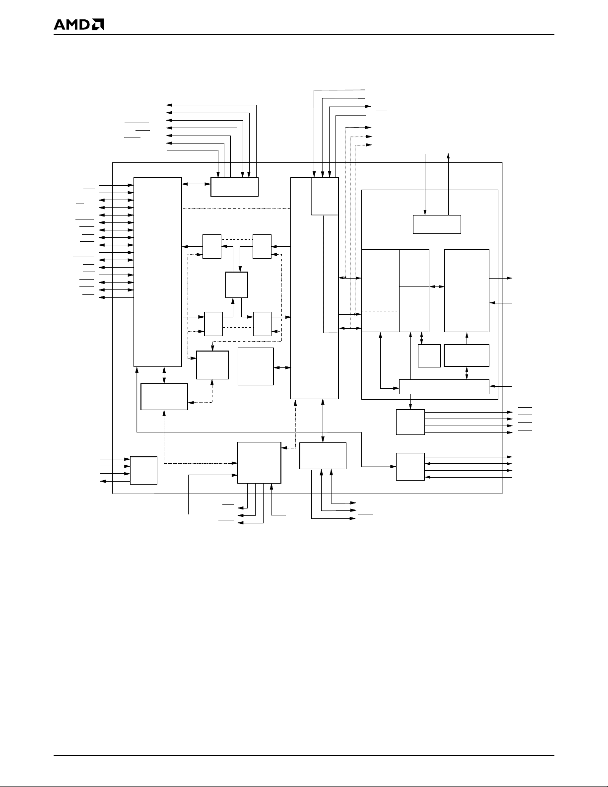
BLOCK DIAGRAM
EBUA_EBA[7:0]
EBDA[15:8]
EBD[7:0]
EROMCS
AS_EBOE
EBWE
EBCLK
PRELIMINARY
MIIRXFRTGE
MIIRXFRTGD
SFBD
EAR
RXD[3:0],TXD[3:0]
MDIO
MDC
XTAL1 XTAL2
CLK
RST
AD[31:0]
C/BE[3:0]
PAR
FRAME
TRDY
IRDY
STOP
IDSEL
DEVSEL
REQ
GNT
PERR
SERR
INTA
TCK
TMS
TDI
TDO
PCI Bus
Interface
Management
JTAG
Port
Control
Unit
Buffer
Unit
Expansion Bus
Bus
Rcv
FIFO
Bus
Xmt
FIFO
FIFO
Control
Interface
12K
SRAM
MAC
Rcv
FIFO
MAC
Xmt
FIFO
Network
Port
Manager
OnNow
Power
Management
Unit
EADI
MII
802.3
MAC
Core
Serial
Management
Interface Unit
MDC
MDIO
MII
Interface
MII
Management
Transmit
Block
Receive
Block
LED
Control
93C46
EEPROM
Interface
Clock
Reference
10/100 PHY Core
(100 BASE-TX)
(100 BASE-FX)
10 BASE-T
Link
Monitor
Negotiation
PHY Control
MLT3
PECL
Auto
TX±
RX±
SDI±
LED0
LED1
LED2
LED3
EECS
EESK
EEDI
EEDO
VAUXDET
PME
RWU
WUMI
PG
4 Am79C973/Am79C975
MCLOCK
MDATA
MIRQ
21510D-1
Page 5

PRELIMINARY
TABLE OF CONTENTS
DISTINCTIVE CHARACTERISTICS . . . . . . . . . . . . . . . . . . . . . . . . . . . . . . . . . . . . . . . 1
GENERAL DESCRIPTION . . . . . . . . . . . . . . . . . . . . . . . . . . . . . . . . . . . . . . . . . . . . . . 2
BLOCK DIAGRAM . . . . . . . . . . . . . . . . . . . . . . . . . . . . . . . . . . . . . . . . . . . . . . . . . . . . 4
TABLE OF CONTENTS . . . . . . . . . . . . . . . . . . . . . . . . . . . . . . . . . . . . . . . . . . . . . . . . 5
LIST OF FIGURES . . . . . . . . . . . . . . . . . . . . . . . . . . . . . . . . . . . . . . . . . . . . . . . . . . . 13
LIST OF TABLES . . . . . . . . . . . . . . . . . . . . . . . . . . . . . . . . . . . . . . . . . . . . . . . . . . . . 15
RELATED AMD PRODUCTS . . . . . . . . . . . . . . . . . . . . . . . . . . . . . . . . . . . . . . . . . . . 17
CONNECTION DIAGRAM (PQR160) - AM79C973 . . . . . . . . . . . . . . . . . . . . . . . . . . 18
CONNECTION DIAGRAM (PQL176) AM79C973 . . . . . . . . . . . . . . . . . . . . . . . . . . . . 19
CONNECTION DIAGRAM (PQR160) - AM79C975 . . . . . . . . . . . . . . . . . . . . . . . . . . 20
CONNECTION DIAGRAM (PQL176) - AM79C975 . . . . . . . . . . . . . . . . . . . . . . . . . . . 21
PIN DESIGNATIONS (PQR160) (Am79C973/Am79C975) . . . . . . . . . . . . . . . . . . . . 22
Listed By Pin Number . . . . . . . . . . . . . . . . . . . . . . . . . . . . . . . . . . . . . . . . . . . . . . . 22
PIN DESIGNATIONS (PQL176) (Am79C973/Am79C975) . . . . . . . . . . . . . . . . . . . . . 23
Listed By Pin Number . . . . . . . . . . . . . . . . . . . . . . . . . . . . . . . . . . . . . . . . . . . . . . . 23
PIN DESIGNATIONS (PQR160, PQL176) . . . . . . . . . . . . . . . . . . . . . . . . . . . . . . . . . 24
Listed By Group . . . . . . . . . . . . . . . . . . . . . . . . . . . . . . . . . . . . . . . . . . . . . . . . . . . 24
PIN DESIGNATIONS . . . . . . . . . . . . . . . . . . . . . . . . . . . . . . . . . . . . . . . . . . . . . . . . . . 25
Listed By Group . . . . . . . . . . . . . . . . . . . . . . . . . . . . . . . . . . . . . . . . . . . . . . . . . . . 25
PIN DESIGNATIONS . . . . . . . . . . . . . . . . . . . . . . . . . . . . . . . . . . . . . . . . . . . . . . . . . . 27
Listed By Driver Type . . . . . . . . . . . . . . . . . . . . . . . . . . . . . . . . . . . . . . . . . . . . . . . 27
ORDERING INFORMATION . . . . . . . . . . . . . . . . . . . . . . . . . . . . . . . . . . . . . . . . . . . . 28
PIN DESCRIPTIONS . . . . . . . . . . . . . . . . . . . . . . . . . . . . . . . . . . . . . . . . . . . . . . . . . . 29
PCI Interface . . . . . . . . . . . . . . . . . . . . . . . . . . . . . . . . . . . . . . . . . . . . . . . . . . . . . . 29
Board Interface . . . . . . . . . . . . . . . . . . . . . . . . . . . . . . . . . . . . . . . . . . . . . . . . . . . . 31
EEPROM Interface . . . . . . . . . . . . . . . . . . . . . . . . . . . . . . . . . . . . . . . . . . . . . . . . . 33
Expansion Bus Interface . . . . . . . . . . . . . . . . . . . . . . . . . . . . . . . . . . . . . . . . . . . . . 33
Media Independent Interface (MII) . . . . . . . . . . . . . . . . . . . . . . . . . . . . . . . . . . . . . 34
External Address Detection Interface . . . . . . . . . . . . . . . . . . . . . . . . . . . . . . . . . . . 36
IEEE 1149.1 (1990) Test Access Port Interface . . . . . . . . . . . . . . . . . . . . . . . . . . . 36
Network Interfaces . . . . . . . . . . . . . . . . . . . . . . . . . . . . . . . . . . . . . . . . . . . . . . . . . 36
Clock Interface . . . . . . . . . . . . . . . . . . . . . . . . . . . . . . . . . . . . . . . . . . . . . . . . . . . . 37
Serial Management Interface (SMI) (Am79C975 only) . . . . . . . . . . . . . . . . . . . . . . 37
Power Supply . . . . . . . . . . . . . . . . . . . . . . . . . . . . . . . . . . . . . . . . . . . . . . . . . . . . . 38
BASIC FUNCTIONS . . . . . . . . . . . . . . . . . . . . . . . . . . . . . . . . . . . . . . . . . . . . . . . . . . 39
System Bus Interface . . . . . . . . . . . . . . . . . . . . . . . . . . . . . . . . . . . . . . . . . . . . . . . 39
Software Interface . . . . . . . . . . . . . . . . . . . . . . . . . . . . . . . . . . . . . . . . . . . . . . . . . . 39
Network Interfaces . . . . . . . . . . . . . . . . . . . . . . . . . . . . . . . . . . . . . . . . . . . . . . . . . 39
Serial Management Interface (Am79C975) . . . . . . . . . . . . . . . . . . . . . . . . . . . . . . 39
MII Interface . . . . . . . . . . . . . . . . . . . . . . . . . . . . . . . . . . . . . . . . . . . . . . . . . . . . . . 39
DETAILED FUNCTIONS . . . . . . . . . . . . . . . . . . . . . . . . . . . . . . . . . . . . . . . . . . . . . . . 40
Slave Bus Interface Unit . . . . . . . . . . . . . . . . . . . . . . . . . . . . . . . . . . . . . . . . . . . . . 40
Slave Configuration Transfers . . . . . . . . . . . . . . . . . . . . . . . . . . . . . . . . . . . . . . . . 40
Slave I/O Transfers . . . . . . . . . . . . . . . . . . . . . . . . . . . . . . . . . . . . . . . . . . . . . . . . . 40
Expansion ROM Transfers. . . . . . . . . . . . . . . . . . . . . . . . . . . . . . . . . . . . . . . . . 43
Slave Cycle Termination . . . . . . . . . . . . . . . . . . . . . . . . . . . . . . . . . . . . . . . . . . 44
Parity Error Response . . . . . . . . . . . . . . . . . . . . . . . . . . . . . . . . . . . . . . . . . . . . 45
Master Bus Interface Unit . . . . . . . . . . . . . . . . . . . . . . . . . . . . . . . . . . . . . . . . . . . . 46
Am79C973/Am79C975 5
Page 6

PRELIMINARY
Bus Acquisition. . . . . . . . . . . . . . . . . . . . . . . . . . . . . . . . . . . . . . . . . . . . . . . . . . 46
Bus Master DMA Transfers . . . . . . . . . . . . . . . . . . . . . . . . . . . . . . . . . . . . . . . . 47
Target Initiated Termination . . . . . . . . . . . . . . . . . . . . . . . . . . . . . . . . . . . . . . . . 50
Master Initiated Termination. . . . . . . . . . . . . . . . . . . . . . . . . . . . . . . . . . . . . . . . 52
Master Abort. . . . . . . . . . . . . . . . . . . . . . . . . . . . . . . . . . . . . . . . . . . . . . . . . . . . 53
Parity Error Response . . . . . . . . . . . . . . . . . . . . . . . . . . . . . . . . . . . . . . . . . . . . 53
Initialization Block DMA Transfers . . . . . . . . . . . . . . . . . . . . . . . . . . . . . . . . . . . 56
Descriptor DMA Transfers . . . . . . . . . . . . . . . . . . . . . . . . . . . . . . . . . . . . . . . . . 58
FIFO DMA Transfers . . . . . . . . . . . . . . . . . . . . . . . . . . . . . . . . . . . . . . . . . . . . . 60
Buffer Management Unit . . . . . . . . . . . . . . . . . . . . . . . . . . . . . . . . . . . . . . . . . . . . . 63
Initialization. . . . . . . . . . . . . . . . . . . . . . . . . . . . . . . . . . . . . . . . . . . . . . . . . . . . . 63
Re-Initialization. . . . . . . . . . . . . . . . . . . . . . . . . . . . . . . . . . . . . . . . . . . . . . . . . . 63
Suspend. . . . . . . . . . . . . . . . . . . . . . . . . . . . . . . . . . . . . . . . . . . . . . . . . . . . . . . 64
Buffer Management . . . . . . . . . . . . . . . . . . . . . . . . . . . . . . . . . . . . . . . . . . . . . . 64
Descriptor Rings. . . . . . . . . . . . . . . . . . . . . . . . . . . . . . . . . . . . . . . . . . . . . . . . . 64
Polling. . . . . . . . . . . . . . . . . . . . . . . . . . . . . . . . . . . . . . . . . . . . . . . . . . . . . . . . . 66
Transmit Descriptor Table Entry. . . . . . . . . . . . . . . . . . . . . . . . . . . . . . . . . . . . . 67
Receive Descriptor Table Entry . . . . . . . . . . . . . . . . . . . . . . . . . . . . . . . . . . . . . 68
Receive Frame Queuing . . . . . . . . . . . . . . . . . . . . . . . . . . . . . . . . . . . . . . . . . . 69
Software Interrupt Timer . . . . . . . . . . . . . . . . . . . . . . . . . . . . . . . . . . . . . . . . . . . . . 69
10/100 Media Access Control . . . . . . . . . . . . . . . . . . . . . . . . . . . . . . . . . . . . . . . . . 70
Transmit and Receive Message Data Encapsulation. . . . . . . . . . . . . . . . . . . . . 70
Destination Address Handling . . . . . . . . . . . . . . . . . . . . . . . . . . . . . . . . . . . . . . 71
Media Access Management. . . . . . . . . . . . . . . . . . . . . . . . . . . . . . . . . . . . . . . . 71
Transmit Operation . . . . . . . . . . . . . . . . . . . . . . . . . . . . . . . . . . . . . . . . . . . . . . . . . 73
Transmit Function Programming . . . . . . . . . . . . . . . . . . . . . . . . . . . . . . . . . . . . 73
Automatic Pad Generation. . . . . . . . . . . . . . . . . . . . . . . . . . . . . . . . . . . . . . . . . 74
Transmit FCS Generation . . . . . . . . . . . . . . . . . . . . . . . . . . . . . . . . . . . . . . . . . 74
Transmit Exception Conditions. . . . . . . . . . . . . . . . . . . . . . . . . . . . . . . . . . . . . . 74
Receive Operation . . . . . . . . . . . . . . . . . . . . . . . . . . . . . . . . . . . . . . . . . . . . . . . . . 75
Receive Function Programming. . . . . . . . . . . . . . . . . . . . . . . . . . . . . . . . . . . . . 75
Address Matching. . . . . . . . . . . . . . . . . . . . . . . . . . . . . . . . . . . . . . . . . . . . . . . . 75
Automatic Pad Stripping. . . . . . . . . . . . . . . . . . . . . . . . . . . . . . . . . . . . . . . . . . . 76
Receive FCS Checking . . . . . . . . . . . . . . . . . . . . . . . . . . . . . . . . . . . . . . . . . . . 77
Receive Exception Conditions . . . . . . . . . . . . . . . . . . . . . . . . . . . . . . . . . . . . . . 77
Loopback Operation . . . . . . . . . . . . . . . . . . . . . . . . . . . . . . . . . . . . . . . . . . . . . . . . 78
Miscellaneous Loopback Features. . . . . . . . . . . . . . . . . . . . . . . . . . . . . . . . . . . 78
Full-Duplex Operation . . . . . . . . . . . . . . . . . . . . . . . . . . . . . . . . . . . . . . . . . . . . 78
Full-Duplex Link Status LED Support. . . . . . . . . . . . . . . . . . . . . . . . . . . . . . . . . 79
10/100 PHY Unit Overview . . . . . . . . . . . . . . . . . . . . . . . . . . . . . . . . . . . . . . . . . . . 79
100BASE-TX Physical Layer . . . . . . . . . . . . . . . . . . . . . . . . . . . . . . . . . . . . . . . . . 79
100BASE-FX (Fiber Interface) . . . . . . . . . . . . . . . . . . . . . . . . . . . . . . . . . . . . . . . . 79
10BASE-T Physical Layer . . . . . . . . . . . . . . . . . . . . . . . . . . . . . . . . . . . . . . . . . . . 79
PHY/MAC Interface . . . . . . . . . . . . . . . . . . . . . . . . . . . . . . . . . . . . . . . . . . . . . . . . 80
Transmit Process . . . . . . . . . . . . . . . . . . . . . . . . . . . . . . . . . . . . . . . . . . . . . . . . 80
Receive Process . . . . . . . . . . . . . . . . . . . . . . . . . . . . . . . . . . . . . . . . . . . . . . . . 80
Internal PHY Loopback Paths . . . . . . . . . . . . . . . . . . . . . . . . . . . . . . . . . . . . . . 80
Encoder . . . . . . . . . . . . . . . . . . . . . . . . . . . . . . . . . . . . . . . . . . . . . . . . . . . . . . . 82
Decoder . . . . . . . . . . . . . . . . . . . . . . . . . . . . . . . . . . . . . . . . . . . . . . . . . . . . . . . 83
6 Am79C973/Am79C975
Page 7

PRELIMINARY
Scrambler/Descrambler . . . . . . . . . . . . . . . . . . . . . . . . . . . . . . . . . . . . . . . . . . . 84
Link Monitor . . . . . . . . . . . . . . . . . . . . . . . . . . . . . . . . . . . . . . . . . . . . . . . . . . . . 84
Far End Fault Generation and Detection . . . . . . . . . . . . . . . . . . . . . . . . . . . . . . 84
MLT-3 and Adaptive Equalization . . . . . . . . . . . . . . . . . . . . . . . . . . . . . . . . . . . 84
Serializer/Deserializer and Clock Recovery. . . . . . . . . . . . . . . . . . . . . . . . . . . . 85
Medium Dependent Interface . . . . . . . . . . . . . . . . . . . . . . . . . . . . . . . . . . . . . . . . . 85
10BASE-T Block . . . . . . . . . . . . . . . . . . . . . . . . . . . . . . . . . . . . . . . . . . . . . . . . . . . 86
Twisted Pair Transmit Function . . . . . . . . . . . . . . . . . . . . . . . . . . . . . . . . . . . . . 86
Twisted Pair Receive Function. . . . . . . . . . . . . . . . . . . . . . . . . . . . . . . . . . . . . . 86
Twisted Pair Interface Status . . . . . . . . . . . . . . . . . . . . . . . . . . . . . . . . . . . . . . . 87
Collision Detect Function . . . . . . . . . . . . . . . . . . . . . . . . . . . . . . . . . . . . . . . . . . 87
Jabber Function . . . . . . . . . . . . . . . . . . . . . . . . . . . . . . . . . . . . . . . . . . . . . . . . . 87
Reverse Polarity Detect . . . . . . . . . . . . . . . . . . . . . . . . . . . . . . . . . . . . . . . . . . . 87
Auto-Negotiation . . . . . . . . . . . . . . . . . . . . . . . . . . . . . . . . . . . . . . . . . . . . . . . . . . . 87
Soft Reset Function . . . . . . . . . . . . . . . . . . . . . . . . . . . . . . . . . . . . . . . . . . . . . . 88
External Address Detection Interface . . . . . . . . . . . . . . . . . . . . . . . . . . . . . . . . . . . 88
External Address Detection Interface: MII Snoop Mode . . . . . . . . . . . . . . . . . . 89
External Address Detection Interface: Receive Frame Tagging . . . . . . . . . . . . 89
Expansion Bus Interface . . . . . . . . . . . . . . . . . . . . . . . . . . . . . . . . . . . . . . . . . . . . . 90
Expansion ROM - Boot Device Access . . . . . . . . . . . . . . . . . . . . . . . . . . . . . . . 90
Direct Flash Access . . . . . . . . . . . . . . . . . . . . . . . . . . . . . . . . . . . . . . . . . . . . . . 93
AMD Flash Programming. . . . . . . . . . . . . . . . . . . . . . . . . . . . . . . . . . . . . . . . . . 95
Direct SRAM Access . . . . . . . . . . . . . . . . . . . . . . . . . . . . . . . . . . . . . . . . . . . . . 96
EEPROM Interface . . . . . . . . . . . . . . . . . . . . . . . . . . . . . . . . . . . . . . . . . . . . . . . . . 98
Automatic EEPROM Read Operation . . . . . . . . . . . . . . . . . . . . . . . . . . . . . . . . 98
LED Support . . . . . . . . . . . . . . . . . . . . . . . . . . . . . . . . . . . . . . . . . . . . . . . . . . . . . . 99
Power Savings Mode . . . . . . . . . . . . . . . . . . . . . . . . . . . . . . . . . . . . . . . . . . . . . . 102
Power Management Support . . . . . . . . . . . . . . . . . . . . . . . . . . . . . . . . . . . . . . 102
Magic Packet Mode . . . . . . . . . . . . . . . . . . . . . . . . . . . . . . . . . . . . . . . . . . . . . . . 104
IEEE 1149.1 (1990) Test Access Port Interface . . . . . . . . . . . . . . . . . . . . . . . . . . 106
Boundary Scan Circuit . . . . . . . . . . . . . . . . . . . . . . . . . . . . . . . . . . . . . . . . . . . 106
TAP Finite State Machine. . . . . . . . . . . . . . . . . . . . . . . . . . . . . . . . . . . . . . . . . 106
Supported Instructions. . . . . . . . . . . . . . . . . . . . . . . . . . . . . . . . . . . . . . . . . . . 106
Boundary Scan Register . . . . . . . . . . . . . . . . . . . . . . . . . . . . . . . . . . . . . . . . . 106
Other Data Registers . . . . . . . . . . . . . . . . . . . . . . . . . . . . . . . . . . . . . . . . . . . . 107
Reset . . . . . . . . . . . . . . . . . . . . . . . . . . . . . . . . . . . . . . . . . . . . . . . . . . . . . . . . . . 107
H_RESET. . . . . . . . . . . . . . . . . . . . . . . . . . . . . . . . . . . . . . . . . . . . . . . . . . . . . 107
S_RESET. . . . . . . . . . . . . . . . . . . . . . . . . . . . . . . . . . . . . . . . . . . . . . . . . . . . . 107
STOP . . . . . . . . . . . . . . . . . . . . . . . . . . . . . . . . . . . . . . . . . . . . . . . . . . . . . . . . 107
Power on Reset . . . . . . . . . . . . . . . . . . . . . . . . . . . . . . . . . . . . . . . . . . . . . . . . 108
Software Access . . . . . . . . . . . . . . . . . . . . . . . . . . . . . . . . . . . . . . . . . . . . . . . . . . 108
PCI Configuration Registers. . . . . . . . . . . . . . . . . . . . . . . . . . . . . . . . . . . . . . . 108
I/O Resources . . . . . . . . . . . . . . . . . . . . . . . . . . . . . . . . . . . . . . . . . . . . . . . . . 109
USER ACCESSIBLE REGISTERS . . . . . . . . . . . . . . . . . . . . . . . . . . . . . . . . . . . . . . 112
PCI Configuration Registers . . . . . . . . . . . . . . . . . . . . . . . . . . . . . . . . . . . . . . . . . 113
PCI Vendor ID Register . . . . . . . . . . . . . . . . . . . . . . . . . . . . . . . . . . . . . . . . . . 113
PCI Device ID Register . . . . . . . . . . . . . . . . . . . . . . . . . . . . . . . . . . . . . . . . . . 113
PCI Command Register . . . . . . . . . . . . . . . . . . . . . . . . . . . . . . . . . . . . . . . . . . 114
PCI Status Register . . . . . . . . . . . . . . . . . . . . . . . . . . . . . . . . . . . . . . . . . . . . . 115
Am79C973/Am79C975 7
Page 8

PRELIMINARY
PCI Revision ID Register . . . . . . . . . . . . . . . . . . . . . . . . . . . . . . . . . . . . . . . . . 116
PCI Programming Interface Register . . . . . . . . . . . . . . . . . . . . . . . . . . . . . . . . 116
PCI Sub-Class Register . . . . . . . . . . . . . . . . . . . . . . . . . . . . . . . . . . . . . . . . . . 117
PCI Base-Class Register . . . . . . . . . . . . . . . . . . . . . . . . . . . . . . . . . . . . . . . . . 117
PCI Latency Timer Register. . . . . . . . . . . . . . . . . . . . . . . . . . . . . . . . . . . . . . . 117
PCI Header Type Register. . . . . . . . . . . . . . . . . . . . . . . . . . . . . . . . . . . . . . . . 117
PCI I/O Base Address Register . . . . . . . . . . . . . . . . . . . . . . . . . . . . . . . . . . . . 117
PCI Memory Mapped I/O Base Address Register . . . . . . . . . . . . . . . . . . . . . . 118
PCI Subsystem Vendor ID Register. . . . . . . . . . . . . . . . . . . . . . . . . . . . . . . . . 119
PCI Subsystem ID Register . . . . . . . . . . . . . . . . . . . . . . . . . . . . . . . . . . . . . . . 119
PCI Expansion ROM Base Address Register . . . . . . . . . . . . . . . . . . . . . . . . . 119
PCI Capabilities Pointer Register. . . . . . . . . . . . . . . . . . . . . . . . . . . . . . . . . . . 120
PCI Interrupt Line Register. . . . . . . . . . . . . . . . . . . . . . . . . . . . . . . . . . . . . . . . 120
PCI Interrupt Pin Register . . . . . . . . . . . . . . . . . . . . . . . . . . . . . . . . . . . . . . . . 120
PCI MIN_GNT Register . . . . . . . . . . . . . . . . . . . . . . . . . . . . . . . . . . . . . . . . . . 120
PCI MAX_LAT Register . . . . . . . . . . . . . . . . . . . . . . . . . . . . . . . . . . . . . . . . . . 120
PCI Capability Identifier Register . . . . . . . . . . . . . . . . . . . . . . . . . . . . . . . . . . . 120
PCI Next Item Pointer Register . . . . . . . . . . . . . . . . . . . . . . . . . . . . . . . . . . . . 120
PCI Power Management Capabilities Register (PMC). . . . . . . . . . . . . . . . . . . 121
PCI Power Management Control/Status Register (PMCSR) . . . . . . . . . . . . . . 121
PCI PMCSR Bridge Support Extensions Register . . . . . . . . . . . . . . . . . . . . . . 122
PCI Data Register . . . . . . . . . . . . . . . . . . . . . . . . . . . . . . . . . . . . . . . . . . . . . . 122
RAP Register . . . . . . . . . . . . . . . . . . . . . . . . . . . . . . . . . . . . . . . . . . . . . . . . . . . . 122
RAP: Register Address Port. . . . . . . . . . . . . . . . . . . . . . . . . . . . . . . . . . . . . . . 123
Control and Status Registers . . . . . . . . . . . . . . . . . . . . . . . . . . . . . . . . . . . . . . . . 123
CSR0: Am79C973/Am79C975 Controller Status and Control Register. . . . . . 123
CSR1: Initialization Block Address 0 . . . . . . . . . . . . . . . . . . . . . . . . . . . . . . . . 126
CSR2: Initialization Block Address 1 . . . . . . . . . . . . . . . . . . . . . . . . . . . . . . . . 126
CSR3: Interrupt Masks and Deferral Control . . . . . . . . . . . . . . . . . . . . . . . . . . 126
CSR4: Test and Features Control . . . . . . . . . . . . . . . . . . . . . . . . . . . . . . . . . . 129
CSR5: Extended Control and Interrupt 1 . . . . . . . . . . . . . . . . . . . . . . . . . . . . . 130
CSR6: RX/TX Descriptor Table Length . . . . . . . . . . . . . . . . . . . . . . . . . . . . . . 133
CSR7: Extended Control and Interrupt 2 . . . . . . . . . . . . . . . . . . . . . . . . . . . . . 133
CSR8: Logical Address Filter 0 . . . . . . . . . . . . . . . . . . . . . . . . . . . . . . . . . . . . 136
CSR9: Logical Address Filter 1 . . . . . . . . . . . . . . . . . . . . . . . . . . . . . . . . . . . . 136
CSR10: Logical Address Filter 2 . . . . . . . . . . . . . . . . . . . . . . . . . . . . . . . . . . . 137
CSR11: Logical Address Filter 3 . . . . . . . . . . . . . . . . . . . . . . . . . . . . . . . . . . . 137
CSR12: Physical Address Register 0. . . . . . . . . . . . . . . . . . . . . . . . . . . . . . . . 137
CSR13: Physical Address Register 1. . . . . . . . . . . . . . . . . . . . . . . . . . . . . . . . 137
CSR14: Physical Address Register 2. . . . . . . . . . . . . . . . . . . . . . . . . . . . . . . . 137
CSR15: Mode . . . . . . . . . . . . . . . . . . . . . . . . . . . . . . . . . . . . . . . . . . . . . . . . . . 138
CSR16: Initialization Block Address Lower . . . . . . . . . . . . . . . . . . . . . . . . . . . 139
CSR17: Initialization Block Address Upper . . . . . . . . . . . . . . . . . . . . . . . . . . . 140
CSR18: Current Receive Buffer Address Lower . . . . . . . . . . . . . . . . . . . . . . . 140
CSR19: Current Receive Buffer Address Upper . . . . . . . . . . . . . . . . . . . . . . . 140
CSR20: Current Transmit Buffer Address Lower. . . . . . . . . . . . . . . . . . . . . . . 140
CSR21: Current Transmit Buffer Address Upper. . . . . . . . . . . . . . . . . . . . . . . 140
CSR22: Next Receive Buffer Address Lower. . . . . . . . . . . . . . . . . . . . . . . . . . 140
CSR23: Next Receive Buffer Address Upper. . . . . . . . . . . . . . . . . . . . . . . . . . 140
8 Am79C973/Am79C975
Page 9

PRELIMINARY
CSR24: Base Address of Receive Ring Lower . . . . . . . . . . . . . . . . . . . . . . . . 141
CSR25: Base Address of Receive Ring Upper . . . . . . . . . . . . . . . . . . . . . . . . 141
CSR26: Next Receive Descriptor Address Lower . . . . . . . . . . . . . . . . . . . . . . 141
CSR27: Next Receive Descriptor Address Upper . . . . . . . . . . . . . . . . . . . . . . 141
CSR28: Current Receive Descriptor Address Lower . . . . . . . . . . . . . . . . . . . . 141
CSR29: Current Receive Descriptor Address Upper . . . . . . . . . . . . . . . . . . . . 141
CSR30: Base Address of Transmit Ring Lower. . . . . . . . . . . . . . . . . . . . . . . . 141
CSR31: Base Address of Transmit Ring Upper. . . . . . . . . . . . . . . . . . . . . . . . 142
CSR32: Next Transmit Descriptor Address Lower. . . . . . . . . . . . . . . . . . . . . . 142
CSR33: Next Transmit Descriptor Address Upper. . . . . . . . . . . . . . . . . . . . . . 142
CSR34: Current Transmit Descriptor Address Lower . . . . . . . . . . . . . . . . . . . 142
CSR35: Current Transmit Descriptor Address Upper . . . . . . . . . . . . . . . . . . . 142
CSR36: Next Next Receive Descriptor Address Lower . . . . . . . . . . . . . . . . . . 142
CSR37: Next Next Receive Descriptor Address Upper . . . . . . . . . . . . . . . . . . 142
CSR38: Next Next Transmit Descriptor Address Lower. . . . . . . . . . . . . . . . . . 143
CSR39: Next Next Transmit Descriptor Address Uper. . . . . . . . . . . . . . . . . . . 143
CSR40: Current Receive Byte Count. . . . . . . . . . . . . . . . . . . . . . . . . . . . . . . . 143
CSR41: Current Receive Status. . . . . . . . . . . . . . . . . . . . . . . . . . . . . . . . . . . . 143
CSR42: Current Transmit Byte Count . . . . . . . . . . . . . . . . . . . . . . . . . . . . . . . 143
CSR43: Current Transmit Status . . . . . . . . . . . . . . . . . . . . . . . . . . . . . . . . . . . 143
CSR44: Next Receive Byte Count . . . . . . . . . . . . . . . . . . . . . . . . . . . . . . . . . . 143
CSR45: Next Receive Status. . . . . . . . . . . . . . . . . . . . . . . . . . . . . . . . . . . . . . 144
CSR46: Transmit Poll Time Counter . . . . . . . . . . . . . . . . . . . . . . . . . . . . . . . . 144
CSR47: Transmit Polling Interval. . . . . . . . . . . . . . . . . . . . . . . . . . . . . . . . . . . 144
CSR48: Receive Poll Time Counter. . . . . . . . . . . . . . . . . . . . . . . . . . . . . . . . . 145
CSR49: Receive Polling Interval . . . . . . . . . . . . . . . . . . . . . . . . . . . . . . . . . . . 145
CSR58: Software Style. . . . . . . . . . . . . . . . . . . . . . . . . . . . . . . . . . . . . . . . . . . 145
CSR60: Previous Transmit Descriptor Address Lower . . . . . . . . . . . . . . . . . . 147
CSR61: Previous Transmit Descriptor Address Upper . . . . . . . . . . . . . . . . . . 148
CSR62: Previous Transmit Byte Count . . . . . . . . . . . . . . . . . . . . . . . . . . . . . . 148
CSR63: Previous Transmit Status . . . . . . . . . . . . . . . . . . . . . . . . . . . . . . . . . . 148
CSR64: Next Transmit Buffer Address Lower . . . . . . . . . . . . . . . . . . . . . . . . . 148
CSR65: Next Transmit Buffer Address Upper . . . . . . . . . . . . . . . . . . . . . . . . . 148
CSR66: Next Transmit Byte Count. . . . . . . . . . . . . . . . . . . . . . . . . . . . . . . . . . 148
CSR67: Next Transmit Status . . . . . . . . . . . . . . . . . . . . . . . . . . . . . . . . . . . . . 149
CSR72: Receive Ring Counter. . . . . . . . . . . . . . . . . . . . . . . . . . . . . . . . . . . . . 149
CSR74: Transmit Ring Counter . . . . . . . . . . . . . . . . . . . . . . . . . . . . . . . . . . . . 149
CSR76: Receive Ring Length . . . . . . . . . . . . . . . . . . . . . . . . . . . . . . . . . . . . . 149
CSR78: Transmit Ring Length . . . . . . . . . . . . . . . . . . . . . . . . . . . . . . . . . . . . . 149
CSR80: DMA Transfer Counter and FIFO Threshold Control . . . . . . . . . . . . . 150
CSR82: Transmit Descriptor Address Pointer Lower. . . . . . . . . . . . . . . . . . . . 152
CSR84: DMA Address Register Lower . . . . . . . . . . . . . . . . . . . . . . . . . . . . . . 152
CSR85: DMA Address Register Upper . . . . . . . . . . . . . . . . . . . . . . . . . . . . . . 152
CSR86: Buffer Byte Counter . . . . . . . . . . . . . . . . . . . . . . . . . . . . . . . . . . . . . . 152
CSR88: Chip ID Register Lower. . . . . . . . . . . . . . . . . . . . . . . . . . . . . . . . . . . . 152
CSR89: Chip ID Register Upper. . . . . . . . . . . . . . . . . . . . . . . . . . . . . . . . . . . . 153
CSR92: Ring Length Conversion. . . . . . . . . . . . . . . . . . . . . . . . . . . . . . . . . . . 153
CSR100: Bus Timeout . . . . . . . . . . . . . . . . . . . . . . . . . . . . . . . . . . . . . . . . . . . 153
CSR112: Missed Frame Count . . . . . . . . . . . . . . . . . . . . . . . . . . . . . . . . . . . . 154
Am79C973/Am79C975 9
Page 10

PRELIMINARY
CSR114: Receive Collision Count . . . . . . . . . . . . . . . . . . . . . . . . . . . . . . . . . . 154
CSR116: OnNow Power Mode Register . . . . . . . . . . . . . . . . . . . . . . . . . . . . . 154
CSR122: Advanced Feature Control . . . . . . . . . . . . . . . . . . . . . . . . . . . . . . . . 156
CSR124: Test Register 1 . . . . . . . . . . . . . . . . . . . . . . . . . . . . . . . . . . . . . . . . . 156
CSR125: MAC Enhanced Configuration Control . . . . . . . . . . . . . . . . . . . . . . . 156
Bus Configuration Registers . . . . . . . . . . . . . . . . . . . . . . . . . . . . . . . . . . . . . . . . . 157
BCR0: Master Mode Read Active . . . . . . . . . . . . . . . . . . . . . . . . . . . . . . . . . . 157
BCR1: Master Mode Write Active. . . . . . . . . . . . . . . . . . . . . . . . . . . . . . . . . . . 158
BCR2: Miscellaneous Configuration. . . . . . . . . . . . . . . . . . . . . . . . . . . . . . . . . 162
BCR4: LED 0 Status. . . . . . . . . . . . . . . . . . . . . . . . . . . . . . . . . . . . . . . . . . . . . 164
BCR5: LED1 Status . . . . . . . . . . . . . . . . . . . . . . . . . . . . . . . . . . . . . . . . . . . . . 166
BCR6: LED2 Status . . . . . . . . . . . . . . . . . . . . . . . . . . . . . . . . . . . . . . . . . . . . . 168
BCR7: LED3 Status . . . . . . . . . . . . . . . . . . . . . . . . . . . . . . . . . . . . . . . . . . . . . 169
BCR9: Full-Duplex Control. . . . . . . . . . . . . . . . . . . . . . . . . . . . . . . . . . . . . . . . 171
BCR16: I/O Base Address Lower. . . . . . . . . . . . . . . . . . . . . . . . . . . . . . . . . . . 172
BCR17: I/O Base Address Upper. . . . . . . . . . . . . . . . . . . . . . . . . . . . . . . . . . . 172
BCR18: Burst and Bus Control Register . . . . . . . . . . . . . . . . . . . . . . . . . . . . . 172
BCR19: EEPROM Control and Status . . . . . . . . . . . . . . . . . . . . . . . . . . . . . . . 175
BCR20: Software Style. . . . . . . . . . . . . . . . . . . . . . . . . . . . . . . . . . . . . . . . . . . 178
BCR22: PCI Latency Register . . . . . . . . . . . . . . . . . . . . . . . . . . . . . . . . . . . . . 179
BCR23: PCI Subsystem Vendor ID Register . . . . . . . . . . . . . . . . . . . . . . . . . . 180
BCR24: PCI Subsystem ID Register . . . . . . . . . . . . . . . . . . . . . . . . . . . . . . . . 180
BCR25: SRAM Size Register. . . . . . . . . . . . . . . . . . . . . . . . . . . . . . . . . . . . . . 180
BCR26: SRAM Boundary Register. . . . . . . . . . . . . . . . . . . . . . . . . . . . . . . . . . 181
BCR27: SRAM Interface Control Register . . . . . . . . . . . . . . . . . . . . . . . . . . . . 181
BCR28: Expansion Bus Port Address Lower
(Used for Flash/EPROM and SRAM Accesses) . . . . . . . . . . . . . . . . . . . . . 183
BCR29: Expansion Port Address Upper
(Used for Flash/EPROM Accesses) . . . . . . . . . . . . . . . . . . . . . . . . . . . . . . 183
BCR30: Expansion Bus Data Port Register. . . . . . . . . . . . . . . . . . . . . . . . . . . 184
BCR31: Software Timer Register. . . . . . . . . . . . . . . . . . . . . . . . . . . . . . . . . . . 184
BCR32: PHY Control and Status Register. . . . . . . . . . . . . . . . . . . . . . . . . . . . 185
BCR33: PHY Address Register . . . . . . . . . . . . . . . . . . . . . . . . . . . . . . . . . . . . 187
BCR34: PHY Management Data Register. . . . . . . . . . . . . . . . . . . . . . . . . . . . 187
BCR35: PCI Vendor ID Register . . . . . . . . . . . . . . . . . . . . . . . . . . . . . . . . . . . 187
BCR36: PCI Power Management Capabilities (PMC) Alias Register . . . . . . . 188
BCR37: PCI DATA Register Zero (DATA0) Alias Register . . . . . . . . . . . . . . . 188
BCR38: PCI DATA Register One (DATA1) Alias Register. . . . . . . . . . . . . . . . 188
BCR39: PCI DATA Register Two (DATA2) Alias Register. . . . . . . . . . . . . . . . 189
BCR40: PCI DATA Register Three (DATA3) Alias Register . . . . . . . . . . . . . . 189
BCR41: PCI DATA Register Four (DATA4) Alias Register . . . . . . . . . . . . . . . 189
BCR42: PCI DATA Register Five (DATA5) Alias Register. . . . . . . . . . . . . . . . 190
BCR43: PCI DATA Register Six (DATA6) Alias Register. . . . . . . . . . . . . . . . . 190
BCR44: PCI DATA Register Seven (DATA7) Alias Register . . . . . . . . . . . . . . 191
BCR45: OnNow Pattern Matching Register 1 . . . . . . . . . . . . . . . . . . . . . . . . . 191
BCR46: OnNow Pattern Matching Register 2 . . . . . . . . . . . . . . . . . . . . . . . . . 191
BCR47: OnNow Pattern Matching Register 3 . . . . . . . . . . . . . . . . . . . . . . . . . 192
BCR48-BCR55: Reserved Locations for Am79C975. . . . . . . . . . . . . . . . . . . . 192
PHY Management Registers (ANRs) . . . . . . . . . . . . . . . . . . . . . . . . . . . . . . . . . . 192
10 Am79C973/Am79C975
Page 11

PRELIMINARY
ANR1: Status Register (Register 1). . . . . . . . . . . . . . . . . . . . . . . . . . . . . . . . . 195
ANR2 and ANR3: PHY Identifier (Registers 2 and 3) . . . . . . . . . . . . . . . . . . . 196
ANR4: Auto-Negotiation Advertisement Register (Register 4). . . . . . . . . . . . . 197
ANR5: Auto-Negotiation Link Partner Ability Register (Register 5) . . . . . . . . . 198
ANR6: Auto-Negotiation Expansion Register (Register 6). . . . . . . . . . . . . . . . 199
ANR7: Auto-Negotiation Next Page Register (Register 7). . . . . . . . . . . . . . . . 199
Reserved Registers (Registers 8-15, 20-23, and 25-31) . . . . . . . . . . . . . . . . . 199
ANR16: INTERRUPT Status and Enable Register (Register 16). . . . . . . . . . . 200
ANR17: PHY Control/Status Register (Register 17) . . . . . . . . . . . . . . . . . . . . 200
ANR18: Descrambler Resynchronization Timer Register (Register 18) . . . . . 202
ANR19: PHY Management Extension Register (Register 19) . . . . . . . . . . . . . 202
ANR24: Summary Status Register (Register 24). . . . . . . . . . . . . . . . . . . . . . . 202
Initialization Block . . . . . . . . . . . . . . . . . . . . . . . . . . . . . . . . . . . . . . . . . . . . . . . . . 203
Receive Descriptors . . . . . . . . . . . . . . . . . . . . . . . . . . . . . . . . . . . . . . . . . . . . . . . 205
Transmit Descriptors . . . . . . . . . . . . . . . . . . . . . . . . . . . . . . . . . . . . . . . . . . . . . . . 209
REGISTER SUMMARY . . . . . . . . . . . . . . . . . . . . . . . . . . . . . . . . . . . . . . . . . . . . . . . 213
PCI Configuration Registers . . . . . . . . . . . . . . . . . . . . . . . . . . . . . . . . . . . . . . . . . 213
Control and Status Registers . . . . . . . . . . . . . . . . . . . . . . . . . . . . . . . . . . . . . . . . 214
Bus Configuration Registers . . . . . . . . . . . . . . . . . . . . . . . . . . . . . . . . . . . . . . . . . 218
PHY Management Registers . . . . . . . . . . . . . . . . . . . . . . . . . . . . . . . . . . . . . . . . 219
PROGRAMMABLE REGISTER SUMMARY . . . . . . . . . . . . . . . . . . . . . . . . . . . . . . . 220
Am79C973/Am79C975 Control and Status Registers . . . . . . . . . . . . . . . . . . . . . 220
Am79C973/Am79C975 Bus Configuration Registers . . . . . . . . . . . . . . . . . . . . . . 222
ABSOLUTE MAXIMUM RATINGS . . . . . . . . . . . . . . . . . . . . . . . . . . . . . . . . . . . . . . 224
SWITCHING CHARACTERISTICS: BUS INTERFACE . . . . . . . . . . . . . . . . . . . . . . 227
SWITCHING CHARACTERISTICS: EXTERNAL ADDRESS
DETECTION INTERFACE . . . . . . . . . . . . . . . . . . . . . . . . . . . . . . . . . . . . . . . . . . 229
EXTERNAL CLOCK . . . . . . . . . . . . . . . . . . . . . . . . . . . . . . . . . . . . . . . . . . . . . . . . . 231
SWITCHING WAVEFORMS . . . . . . . . . . . . . . . . . . . . . . . . . . . . . . . . . . . . . . . . . . . 234
SWITCHING TEST CIRCUITS . . . . . . . . . . . . . . . . . . . . . . . . . . . . . . . . . . . . . . . . . 235
SWITCHING WAVEFORMS: SYSTEM BUS INTERFACE . . . . . . . . . . . . . . . . . . . . 236
SWITCHING WAVEFORMS: EXPANSION BUS INTERFACE . . . . . . . . . . . . . . . . 240
PHYSICAL DIMENSIONS* . . . . . . . . . . . . . . . . . . . . . . . . . . . . . . . . . . . . . . . . . . . . 242
PQR160 . . . . . . . . . . . . . . . . . . . . . . . . . . . . . . . . . . . . . . . . . . . . . . . . . . . . . . . . 242
PQL176 . . . . . . . . . . . . . . . . . . . . . . . . . . . . . . . . . . . . . . . . . . . . . . . . . . . . . . . . . 243
APPENDIX A: PCnet™-FAST III Recommended Magnetics . . . . . . . . . . . . . . . . 244
APPENDIX B: SERIAL MANAGEMENT INTERFACE UNIT
(AM79C975 ONLY) . . . . . . . . . . . . . . . . . . . . . . . . . . . . . . . . . . . . . . . . . . . . . . . 245
Overview . . . . . . . . . . . . . . . . . . . . . . . . . . . . . . . . . . . . . . . . . . . . . . . . . . . . . . . . 245
Am79C975 PIN DESIGNATIONS . . . . . . . . . . . . . . . . . . . . . . . . . . . . . . . . . . . . . 245
Basic Operation . . . . . . . . . . . . . . . . . . . . . . . . . . . . . . . . . . . . . . . . . . . . . . . . . . 246
Am79C975 Slave Address . . . . . . . . . . . . . . . . . . . . . . . . . . . . . . . . . . . . . . . . . . 247
Register Access . . . . . . . . . . . . . . . . . . . . . . . . . . . . . . . . . . . . . . . . . . . . . . . . . . 247
Detailed Functions . . . . . . . . . . . . . . . . . . . . . . . . . . . . . . . . . . . . . . . . . . . . . . . . 250
Transmit Operation . . . . . . . . . . . . . . . . . . . . . . . . . . . . . . . . . . . . . . . . . . . . . . . . 251
Receive Operation . . . . . . . . . . . . . . . . . . . . . . . . . . . . . . . . . . . . . . . . . . . . . . . . 252
Loopback Operation . . . . . . . . . . . . . . . . . . . . . . . . . . . . . . . . . . . . . . . . . . . . . . . 254
User Accessible Registers . . . . . . . . . . . . . . . . . . . . . . . . . . . . . . . . . . . . . . . . . . 254
Device ID Registers . . . . . . . . . . . . . . . . . . . . . . . . . . . . . . . . . . . . . . . . . . . . . . . 254
Am79C973/Am79C975 11
Page 12

PRELIMINARY
Node ID Registers . . . . . . . . . . . . . . . . . . . . . . . . . . . . . . . . . . . . . . . . . . . . . . . . 256
Device Status Registers . . . . . . . . . . . . . . . . . . . . . . . . . . . . . . . . . . . . . . . . . . . . 258
Control and Status Registers . . . . . . . . . . . . . . . . . . . . . . . . . . . . . . . . . . . . . . . . 259
Register Summary . . . . . . . . . . . . . . . . . . . . . . . . . . . . . . . . . . . . . . . . . . . . . . . . 264
Am79C975 EEPROM Map . . . . . . . . . . . . . . . . . . . . . . . . . . . . . . . . . . . . . . . . . . 264
Am79C975 EEPROM Map . . . . . . . . . . . . . . . . . . . . . . . . . . . . . . . . . . . . . . . . . . 265
Absolute Maximum Ratings . . . . . . . . . . . . . . . . . . . . . . . . . . . . . . . . . . . . . . . . . 266
Operating Ranges . . . . . . . . . . . . . . . . . . . . . . . . . . . . . . . . . . . . . . . . . . . . . . . . . 266
DC Characteristics . . . . . . . . . . . . . . . . . . . . . . . . . . . . . . . . . . . . . . . . . . . . . . . . 266
Switching Characteristics . . . . . . . . . . . . . . . . . . . . . . . . . . . . . . . . . . . . . . . . . . . 266
Switching Waveforms . . . . . . . . . . . . . . . . . . . . . . . . . . . . . . . . . . . . . . . . . . . . . . 267
APPENDIX C: MEDIA INDEPENDENT INTERFACE (MII) . . . . . . . . . . . . . . . . . . . . 268
Introduction . . . . . . . . . . . . . . . . . . . . . . . . . . . . . . . . . . . . . . . . . . . . . . . . . . . . . . 268
Auto-Negotiation . . . . . . . . . . . . . . . . . . . . . . . . . . . . . . . . . . . . . . . . . . . . . . . . . . 271
Automatic Network Port Selection . . . . . . . . . . . . . . . . . . . . . . . . . . . . . . . . . . . . 271
External Address Detection Interface . . . . . . . . . . . . . . . . . . . . . . . . . . . . . . . . . . 272
MII management registers . . . . . . . . . . . . . . . . . . . . . . . . . . . . . . . . . . . . . . . . . . 274
Control Register (Register 0) . . . . . . . . . . . . . . . . . . . . . . . . . . . . . . . . . . . . . . . . 274
Status Register (Register 1) . . . . . . . . . . . . . . . . . . . . . . . . . . . . . . . . . . . . . . . . . 275
Auto-Negotiation Advertisement Register (Register 4) . . . . . . . . . . . . . . . . . . . . . 276
Auto-Negotiation Link Partner Ability Register (Register 5) . . . . . . . . . . . . . . . . . 277
Switching Characteristics: Media Independent Interface . . . . . . . . . . . . . . . . . . . 278
Switching Waveforms: Media Independent Interface . . . . . . . . . . . . . . . . . . . . . . 279
Switching Waveforms: External Address Detection Interface . . . . . . . . . . . . . . . . 281
Switching Waveforms: Receive Frame Tag . . . . . . . . . . . . . . . . . . . . . . . . . . . . . 282
APPENDIX D: ALTERNATIVE METHOD FOR INITIALIZATION . . . . . . . . . . . . . . . 283
APPENDIX E: LOOK-AHEAD PACKET PROCESSING (LAPP) CONCEPT . . . . . 284
Introduction . . . . . . . . . . . . . . . . . . . . . . . . . . . . . . . . . . . . . . . . . . . . . . . . . . . . . . 284
Outline of LAPP Flow . . . . . . . . . . . . . . . . . . . . . . . . . . . . . . . . . . . . . . . . . . . . . . 285
LAPP Software Requirements . . . . . . . . . . . . . . . . . . . . . . . . . . . . . . . . . . . . . . . 288
LAPP Rules for Parsing Descriptors . . . . . . . . . . . . . . . . . . . . . . . . . . . . . . . . . . . 288
Some Examples of LAPP Descriptor Interaction . . . . . . . . . . . . . . . . . . . . . . . . . 289
Buffer Size Tuning . . . . . . . . . . . . . . . . . . . . . . . . . . . . . . . . . . . . . . . . . . . . . . . . 290
An Alternative LAPP Flow: Two-Interrupt Method . . . . . . . . . . . . . . . . . . . . . . . . 291
INDEX . . . . . . . . . . . . . . . . . . . . . . . . . . . . . . . . . . . . . . . . . . . . . . . . . . . . . . . . . . . . 294
12 Am79C973/Am79C975
Page 13

PRELIMINARY
LIST OF FIGURES
Figure 1. Slave Configuration Read . . . . . . . . . . . . . . . . . . . . . . . . . . . . . . . . . . . . . . . 41
Figure 2. Slave Configuration Write . . . . . . . . . . . . . . . . . . . . . . . . . . . . . . . . . . . . . . . 41
Figure 3. Slave Read Using I/O Command . . . . . . . . . . . . . . . . . . . . . . . . . . . . . . . . . 42
Figure 4. Slave Write Using Memory Command . . . . . . . . . . . . . . . . . . . . . . . . . . . . . 42
Figure 5. Expansion ROM Read . . . . . . . . . . . . . . . . . . . . . . . . . . . . . . . . . . . . . . . . . 43
Figure 6. Disconnect Of Slave Cycle When Busy . . . . . . . . . . . . . . . . . . . . . . . . . . . . 44
Figure 7. Disconnect Of Slave Burst Transfer - No Host Wait States . . . . . . . . . . . . . 44
Figure 8. Disconnect Of Slave Burst Transfer - Host Inserts Wait States . . . . . . . . . . 45
Figure 9. Address Parity Error Response . . . . . . . . . . . . . . . . . . . . . . . . . . . . . . . . . . 45
Figure 10. Slave Cycle Data Parity Error Response 46
Figure 11. Bus Acquisition . . . . . . . . . . . . . . . . . . . . . . . . . . . . . . . . . . . . . . . . . . . . . . . 47
Figure 12. Non-Burst Read Transfer . . . . . . . . . . . . . . . . . . . . . . . . . . . . . . . . . . . . . . . 48
Figure 13. Burst Read Transfer (EXTREQ = 0, MEMCMD = 0) . . . . . . . . . . . . . . . . . . 48
Figure 14. Non-Burst Write Transfer . . . . . . . . . . . . . . . . . . . . . . . . . . . . . . . . . . . . . . . 49
Figure 15. Burst Write Transfer (EXTREQ = 1) . . . . . . . . . . . . . . . . . . . . . . . . . . . . . . . 50
Figure 16. Disconnect With Data Transfer . . . . . . . . . . . . . . . . . . . . . . . . . . . . . . . . . . 51
Figure 17. Disconnect Without Data Transfer . . . . . . . . . . . . . . . . . . . . . . . . . . . . . . . . 52
Figure 18. Target Abort . . . . . . . . . . . . . . . . . . . . . . . . . . . . . . . . . . . . . . . . . . . . . . . . . 53
Figure 19. Preemption During Non-Burst Transaction . . . . . . . . . . . . . . . . . . . . . . . . . 54
Figure 20. Preemption During Burst Transaction 54
Figure 21. Master Abort . . . . . . . . . . . . . . . . . . . . . . . . . . . . . . . . . . . . . . . . . . . . . . . . . 55
Figure 22. Master Cycle Data Parity Error Response . . . . . . . . . . . . . . . . . . . . . . . . . . 55
Figure 23. Initialization Block Read In Non-Burst Mode 57
Figure 24. Initialization Block Read In Burst Mode 57
Figure 25. Descriptor Ring Read In Non-Burst Mode . . . . . . . . . . . . . . . . . . . . . . . . . . 59
Figure 26. Descriptor Ring Read In Burst Mode . . . . . . . . . . . . . . . . . . . . . . . . . . . . . . 59
Figure 27. Descriptor Ring Write In Non-Burst Mode . . . . . . . . . . . . . . . . . . . . . . . . . . 61
Figure 28. Descriptor Ring Write In Burst Mode . . . . . . . . . . . . . . . . . . . . . . . . . . . . . . 61
Figure 29. FIFO Burst Write At Start Of Unaligned Buffer . . . . . . . . . . . . . . . . . . . . . . . 62
Figure 30. FIFO Burst Write At End Of Unaligned Buffer . . . . . . . . . . . . . . . . . . . . . . . 63
Figure 31. 16-Bit Software Model . . . . . . . . . . . . . . . . . . . . . . . . . . . . . . . . . . . . . . . . . 66
Figure 32. 32-Bit Software Model . . . . . . . . . . . . . . . . . . . . . . . . . . . . . . . . . . . . . . . . . 67
Figure 33. ISO 8802-3 (IEEE/ANSI 802.3) Data Frame . . . . . . . . . . . . . . . . . . . . . . . .74
Figure 34. IEEE 802.3 Frame And Length Field Transmission Order . . . . . . . . . . . . . . 77
Figure 35. 100BASE-X Transmit and Receive Data Paths of the Internal PHY . . . . . . 81
Figure 36. MLT-3 Waveform . . . . . . . . . . . . . . . . . . . . . . . . . . . . . . . . . . . . . . . . . . . . . 85
Figure 37. TX± and RX± Termination 86
Figure 38. 10BASE-T Transmit and Receive Data Paths . . . . . . . . . . . . . . . . . . . . . . . 87
Figure 39. Receive Frame Tagging . . . . . . . . . . . . . . . . . . . . . . . . . . . . . . . . . . . . . . . . 90
Figure 40. Flash Configuration for the Expansion Bus . . . . . . . . . . . . . . . . . . . . . . . . . 91
Figure 41. EPROM Only Configuration for the Expansion Bus (64K EPROM) . . . . . . . 92
Figure 42. EPROM Only Configuration for the Expansion Bus (64K EPROM) 93
Figure 43. Expansion ROM Bus Read Sequence . . . . . . . . . . . . . . . . . . . . . . . . . . . . . 94
Figure 44. Flash Read from Expansion Bus Data Port . . . . . . . . . . . . . . . . . . . . . . . . . 94
Figure 45. Flash Write from Expansion Bus Data Port . . . . . . . . . . . . . . . . . . . . . . . . . 95
Figure 46. Block Diagram No SRAM Configuration . . . . . . . . . . . . . . . . . . . . . . . . . . . . 97
Figure 47. Block Diagram Low Latency Receive Configuration . . . . . . . . . . . . . . . . . . 97
Figure 48. LED Control Logic . . . . . . . . . . . . . . . . . . . . . . . . . . . . . . . . . . . . . . . . . . . 102
Am79C973/Am79C975 13
Page 14

PRELIMINARY
Figure 49. OnNow Functional Diagram . . . . . . . . . . . . . . . . . . . . . . . . . . . . . . . . . . . . 103
Figure 50. Pattern Match RAM . . . . . . . . . . . . . . . . . . . . . . . . . . . . . . . . . . . . . . . . . . 105
Figure 51. Address Match Logic . . . . . . . . . . . . . . . . . . . . . . . . . . . . . . . . . . . . . . . . . 205
Figure 52. External Clock Timing . . . . . . . . . . . . . . . . . . . . . . . . . . . . . . . . . . . . . . . . 231
Figure 53. PMD Interface Timing (PECL) . . . . . . . . . . . . . . . . . . . . . . . . . . . . . . . . . . 232
Figure 54. PMD Interface Timing (MLT-3) . . . . . . . . . . . . . . . . . . . . . . . . . . . . . . . . . . 232
Figure 55. 10 Mbps Transmit (TX±) Timing Diagram . . . . . . . . . . . . . . . . . . . . . . . . . 233
Figure 56. 10 Mbps Receive (RX±) Timing Diagram . . . . . . . . . . . . . . . . . . . . . . . . . . 233
Figure 57. Normal and Tri-State Outputs . . . . . . . . . . . . . . . . . . . . . . . . . . . . . . . . . . 235
Figure 58. CLK Waveform for 5 V Signaling . . . . . . . . . . . . . . . . . . . . . . . . . . . . . . . . 236
Figure 59. CLK Waveform for 3.3 V Signaling . . . . . . . . . . . . . . . . . . . . . . . . . . . . . . . 236
Figure 60. Input Setup and Hold Timing . . . . . . . . . . . . . . . . . . . . . . . . . . . . . . . . . . . 236
Figure 61. Output Valid Delay Timing . . . . . . . . . . . . . . . . . . . . . . . . . . . . . . . . . . . . .237
Figure 62. Output Tri-state Delay Timing . . . . . . . . . . . . . . . . . . . . . . . . . . . . . . . . . . 237
Figure 63. EEPROM Read Functional Timing . . . . . . . . . . . . . . . . . . . . . . . . . . . . . . . 2 37
Figure 64. Automatic PREAD EEPROM Timing . . . . . . . . . . . . . . . . . . . . . . . . . . . . . 238
Figure 65. JTAG (IEEE 1149.1) TCK Waveform for 5 V Signaling . . . . . . . . . . . . . . . 238
Figure 66. JTAG (IEEE 1149.1) Test Signal Timing . . . . . . . . . . . . . . . . . . . . . . . . . . 239
Figure 67. EBCLK Waveform . . . . . . . . . . . . . . . . . . . . . . . . . . . . . . . . . . . . . . . . . . . 240
Figure 68. Expansion Bus Read Timing 240
Figure 69. Expansion Bus Write Timing . . . . . . . . . . . . . . . . . . . . . . . . . . . . . . . . . . . 241
Figure 70. Standard Data Transfer on the Serial Management Interface . . . . . . . . . . 247
Figure 71. Data Transfer with Change in Direction (with wait state) . . . . . . . . . . . . . . 247
Figure 72. Write Byte Command . . . . . . . . . . . . . . . . . . . . . . . . . . . . . . . . . . . . . . . . . 248
Figure 73. Read Byte Command . . . . . . . . . . . . . . . . . . . . . . . . . . . . . . . . . . . . . . . . . 2 48
Figure 74. Block Write Command 249
Figure 75. Block Read Command 250
Figure 76. System Management Interface Timing . . . . . . . . . . . . . . . . . . . . . . . . . . . . 267
Figure 77. Media Independent Interface 268
Figure 78. Frame Format at the MII Interface Connection . . . . . . . . . . . . . . . . . . . . . 270
Figure 79. MII Receive Frame Tagging . . . . . . . . . . . . . . . . . . . . . . . . . . . . . . . . . . . .273
Figure 80. Transmit Timing . . . . . . . . . . . . . . . . . . . . . . . . . . . . . . . . . . . . . . . . . . . . . 279
Figure 81. Receive Timing . . . . . . . . . . . . . . . . . . . . . . . . . . . . . . . . . . . . . . . . . . . . . . 279
Figure 82. MDC Waveform . . . . . . . . . . . . . . . . . . . . . . . . . . . . . . . . . . . . . . . . . . . . . 279
Figure 83. Management Data Setup and Hold Timing . . . . . . . . . . . . . . . . . . . . . . . . 280
Figure 84. Management Data Output Valid Delay Timing . . . . . . . . . . . . . . . . . . . . . . 280
Figure 85. Reject Timing - External PHY MII @ 25 MHz . . . . . . . . . . . . . . . . . . . . . . . 281
Figure 86. Reject Timing - External PHY MII @ 2.5 MHz 281
Figure 87. Receive Frame Tag Timing with Media Independent Interface . . . . . . . . . 282
Figure 88. LAPP Timeline . . . . . . . . . . . . . . . . . . . . . . . . . . . . . . . . . . . . . . . . . . . . . . 287
Figure 89. LAPP 3 Buffer Grouping . . . . . . . . . . . . . . . . . . . . . . . . . . . . . . . . . . . . . . . 288
Figure 90. LAPP Timeline for Two-Interrupt Method . . . . . . . . . . . . . . . . . . . . . . . . . .292
Figure 91. LAPP 3 Buffer Grouping for Two-interrupt Method . . . . . . . . . . . . . . . . . . 293
14 Am79C973/Am79C975
Page 15

PRELIMINARY
LIST OF TABLES
Table 1. Interrupt Flags. . . . . . . . . . . . . . . . . . . . . . . . . . . . . . . . . . . . . . . . . . . . . . . . 30
Table 2. SDI± Settings for Transceiver Operation . . . . . . . . . . . . . . . . . . . . . . . . . . . 37
Table 3. Slave Commands . . . . . . . . . . . . . . . . . . . . . . . . . . . . . . . . . . . . . . . . . . . . . 40
Table 4. Master Commands . . . . . . . . . . . . . . . . . . . . . . . . . . . . . . . . . . . . . . . . . . . . 46
Table 5. Descriptor Read Sequence. . . . . . . . . . . . . . . . . . . . . . . . . . . . . . . . . . . . . . 58
Table 6. Descriptor Write Sequence. . . . . . . . . . . . . . . . . . . . . . . . . . . . . . . . . . . . . . 60
Table 7. Receive Address Match . . . . . . . . . . . . . . . . . . . . . . . . . . . . . . . . . . . . . . . . 76
Table 8. Encoder Code-Group Mapping . . . . . . . . . . . . . . . . . . . . . . . . . . . . . . . . . . . 82
Table 9. Decoder Code-Group Mapping . . . . . . . . . . . . . . . . . . . . . . . . . . . . . . . . . . . 83
Table 10. Auto-Negotiation Capabilities. . . . . . . . . . . . . . . . . . . . . . . . . . . . . . . . . . . . 88
Table 11. EADI Operations. . . . . . . . . . . . . . . . . . . . . . . . . . . . . . . . . . . . . . . . . . . . . . 89
Table 12. Am29Fxxx Flash Command . . . . . . . . . . . . . . . . . . . . . . . . . . . . . . . . . . . . . 95
Table 13. Am79C973 EEPROM Map . . . . . . . . . . . . . . . . . . . . . . . . . . . . . . . . . . . . . 100
Table 14. Am79C975 EEPROM Map . . . . . . . . . . . . . . . . . . . . . . . . . . . . . . . . . . . . . 101
Table 15. LED Default Configuration . . . . . . . . . . . . . . . . . . . . . . . . . . . . . . . . . . . . . 102
Table 16. IEEE 1149.1 Supported Instruction Summary . . . . . . . . . . . . . . . . . . . . . . 106
Table 17. BSR Mode Of Operation. . . . . . . . . . . . . . . . . . . . . . . . . . . . . . . . . . . . . . . 107
Table 18. Device ID Register . . . . . . . . . . . . . . . . . . . . . . . . . . . . . . . . . . . . . . . . . . . 107
Table 19. PCI Configuration Space Layout . . . . . . . . . . . . . . . . . . . . . . . . . . . . . . . . . 108
Table 20. I/O Map In Word I/O Mode (DWIO = 0) . . . . . . . . . . . . . . . . . . . . . . . . . . . 110
Table 21. Legal I/O Accesses in Word I/O Mode (DWIO = 0) . . . . . . . . . . . . . . . . . . .111
Table 22. I/O Map In DWord I/O Mode (DWIO =1). . . . . . . . . . . . . . . . . . . . . . . . . . . 111
Table 23. Legal I/O Accesses in Double Word I/O Mode (DWIO =1). . . . . . . . . . . . . 111
Table 24. Loopback Configuration . . . . . . . . . . . . . . . . . . . . . . . . . . . . . . . . . . . . . . . 139
Table 25. Software Styles . . . . . . . . . . . . . . . . . . . . . . . . . . . . . . . . . . . . . . . . . . . . . . 147
Table 26. Receive Watermark Programming . . . . . . . . . . . . . . . . . . . . . . . . . . . . . . . 150
Table 27. Transmit Start Point Programming. . . . . . . . . . . . . . . . . . . . . . . . . . . . . . . 151
Table 28. Transmit Watermark Programming . . . . . . . . . . . . . . . . . . . . . . . . . . . . . . 151
Table 29. BCR Registers (Am79C973) . . . . . . . . . . . . . . . . . . . . . . . . . . . . . . . . . . . 159
Table 30. BCR Registers (Am79C975) . . . . . . . . . . . . . . . . . . . . . . . . . . . . . . . . . . . 161
Table 31. ROMTNG Programming Values. . . . . . . . . . . . . . . . . . . . . . . . . . . . . . . . . 172
Table 32. Interface Pin Assignment . . . . . . . . . . . . . . . . . . . . . . . . . . . . . . . . . . . . . . . 177
Table 33. Software Styles. . . . . . . . . . . . . . . . . . . . . . . . . . . . . . . . . . . . . . . . . . . . . . 179
Table 34. SRAM_BND Programming. . . . . . . . . . . . . . . . . . . . . . . . . . . . . . . . . . . . . 181
Table 35. EBCS Values . . . . . . . . . . . . . . . . . . . . . . . . . . . . . . . . . . . . . . . . . . . . . . . 182
Table 36. CLK_FAC Values. . . . . . . . . . . . . . . . . . . . . . . . . . . . . . . . . . . . . . . . . . . . 183
Table 37. FMDC Values. . . . . . . . . . . . . . . . . . . . . . . . . . . . . . . . . . . . . . . . . . . . . . . 185
Table 38. APDW Values. . . . . . . . . . . . . . . . . . . . . . . . . . . . . . . . . . . . . . . . . . . . . . . 186
Table 39. Am79C973/Am79C975 Internal PHY Management Register Set . . . . . . . 193
Table 40. ANR0: PHY Control Register (Register 0) . . . . . . . . . . . . . . . . . . . . . . . . . . 194
Table 41. ANR1: PHY Status Register (Register 1) . . . . . . . . . . . . . . . . . . . . . . . . . . 195
Table 42. ANR2: PHY Identifier (Register 2) . . . . . . . . . . . . . . . . . . . . . . . . . . . . . . . . 196
Table 43. ANR3: PHY Identifier (Register 3) . . . . . . . . . . . . . . . . . . . . . . . . . . . . . . . . 196
Table 44. ANR4: Auto-Negotiation Advertisement Register (Register 4) . . . . . . . . . . 197
Table 45. ANR5: Auto-Negotiation Link Partner Ability Register (Register 5)
- Base Page Format . . . . . . . . . . . . . . . . . . . . . . . . . . . . . . . . . . . . . . . . . . . . . . . . . . 198
Table 46. ANR5: Auto-Negotiation Link Partner Ability Register (Register 5)
- Next Page Format . . . . . . . . . . . . . . . . . . . . . . . . . . . . . . . . . . . . . . . . . . . . . . . . . . 198
Am79C973/Am79C975 15
Page 16

PRELIMINARY
Table 47. ANR6: Auto-Negotiation Expansion Register (Register 6) . . . . . . . . . . . . . 199
Table 48. ANR7: Auto-Negotiation Next Page Register (Register 7) . . . . . . . . . . . . . 199
Table 49. ANR16: INTERRUPT Status and Enable Register (Register 16) . . . . . . . . 200
Table 50. ANR17: PHY Control/Status Register (Register 17) . . . . . . . . . . . . . . . . . . 201
Table 51. ANR18: Descrambler Resynchronization Timer (Register 18) . . . . . . . . . . 202
Table 52. ANR19: PHY Management Extension Register (Register 19) . . . . . . . . . . . 202
Table 53. ANR24: Summary Status Register (Register 24) . . . . . . . . . . . . . . . . . . . . 203
Table 54. Initialization Block (SSIZE32 = 0) . . . . . . . . . . . . . . . . . . . . . . . . . . . . . . . . 203
Table 55. Initialization Block (SSIZE32 = 1). . . . . . . . . . . . . . . . . . . . . . . . . . . . . . . . 204
Table 56. R/TLEN Decoding (SSIZE32 = 0). . . . . . . . . . . . . . . . . . . . . . . . . . . . . . . . 204
Table 57. R/TLEN Decoding (SSIZE32 = 1). . . . . . . . . . . . . . . . . . . . . . . . . . . . . . . . 204
Table 58. Receive Descriptor (SWSTYLE = 0) . . . . . . . . . . . . . . . . . . . . . . . . . . . . . . 205
Table 59. Receive Descriptor (SWSTYLE = 2) . . . . . . . . . . . . . . . . . . . . . . . . . . . . . . 206
Table 60. Receive Descriptor (SWSTYLE = 3) . . . . . . . . . . . . . . . . . . . . . . . . . . . . . . 206
Table 61. Transmit Descriptor (SWSTYLE = 0) . . . . . . . . . . . . . . . . . . . . . . . . . . . . . 209
Table 62. Transmit Descriptor (SWSTYLE = 2) . . . . . . . . . . . . . . . . . . . . . . . . . . . . . 209
Table 63. Transmit Descriptor (SWSTYLE = 3) . . . . . . . . . . . . . . . . . . . . . . . . . . . . . 209
Table 64. Clock (XTAL1, XCLK = 1) Switching Characteristics . . . . . . . . . . . . . . . . . 231
Table 65. Crystal (XTAL1, XTAL2, XCLK = 0) Requirements . . . . . . . . . . . . . . . . . . 231
Table 66. Crystal (XTAL1, XTAL2, XCLK = 0) Requirements . . . . . . . . . . . . . . . . . . 231
Table 67. Recommended Magnetics Vendors . . . . . . . . . . . . . . . . . . . . . . . . . . . . . . 244
Table 68. Auto-Negotiation Capabilities. . . . . . . . . . . . . . . . . . . . . . . . . . . . . . . . . . . 271
Table 69. EADI Operations. . . . . . . . . . . . . . . . . . . . . . . . . . . . . . . . . . . . . . . . . . . . . 273
Table 70. MII Management Register Set . . . . . . . . . . . . . . . . . . . . . . . . . . . . . . . . . . 274
Table 71. MII Management Control Register (Register 0) . . . . . . . . . . . . . . . . . . . . . .274
Table 72. MII Management Status Register (Register 1) . . . . . . . . . . . . . . . . . . . . . . 275
Table 73. Auto-Negotiation Advertisement Register (Register 4) . . . . . . . . . . . . . . . . 276
Table 74. Technology Ability Field Bit Assignments . . . . . . . . . . . . . . . . . . . . . . . . . . 276
Table 75. Auto-Negotiation Link Partner Ability Register (Register 5)
- Base Page Format . . . . . . . . . . . . . . . . . . . . . . . . . . . . . . . . . . . . . . . . . . . . . . . . . . 277
Table 76. Registers for Alternative Initialization Method (Note 1) . . . . . . . . . . . . . . . . 283
16 Am79C973/Am79C975
Page 17

PRELIMINARY
RELATED AMD PRODUCTS
Part No. Description
Controllers
Am79C90 CMOS Local Area Network Controller for Ethernet (C-LANCE™)
Integrated Controllers
Am79C930 PCnet™-Mobile Single Chip Wireless LAN Media Access Controller
Am79C940 Media Access Controller for Ethernet (MACE™)
Am79C961A PCnet-ISA II Full Duplex Single-Chip Ethernet Controller for ISA Bus
Am79C965 PCnet-32 Single-Chip 32-Bit Ethernet Controller for 486 and VL Buses
Am79C970A PCnet-PCI II Full Duplex Single-Chip Ethernet Controller for PCI Local Bus
Am79C971 PCnet-FAST Single-Chip Full-Duplex 10/100 Mbps Ethernet Controller for PCI Local Bus
Am79C972 PCnet-FAST+ Enhanced 10/100 Mbps PCI Ethernet Controller with OnNow Support
Manchester Encoder/Decoder
Am7992B Serial Interface Adapter (SIA)
Physical Layer Devices (Single-Port)
Am7996 IEEE 802.3/Ethernet/Cheapernet Transceiver
Am79761 Physical Layer 10-Bit Transceiver for Gigabit Ethernet (GigaPHY™-SD)
Am79C98 Twisted Pair Ethernet Transceiver (TPEX)
Am79C100 Twisted Pair Ethernet Transceiver Plus (TPEX+)
Physical Layer Devices (Multi-Port)
Am79C871 Quad Fast Ethernet Transceiver for 100BASE-X Repeaters (QFEXr™)
Am79C988A Quad Integrated Ether net Transceiver (QuIET™)
Am79C989 Quad Ethernet Switching Transceiver (QuEST™)
Integrated Repeater/Hub Devices
Am79C981 Integrated Multiport Repeater Plus (IMR+)
Am79C982 Basic Integrated Multiport Repeater (bIMR)
Am79C983 Integrated Multiport Repeater 2 (IMR2™)
Am79C984A Enhanced Integrated Multiport Repeater (eIMR™)
Am79C985 Enhanced Integrated Multiport Repeater Plus (eIMR+™)
Am79C987 Hardware Implemented Management Information Base (HIMIB™)
Am79C973/Am79C975 17
Page 18
PRELIMINARY
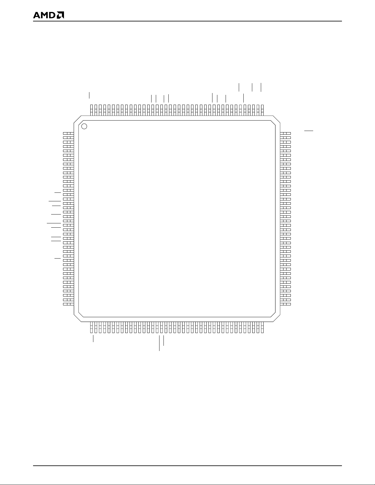
CONNECTION DIAGRAM (PQR160) - Am79C973
C/BE3
AD24
AD25
VSSB
AD26
VDD_PCI
AD27
AD28
AD29
AD30
VSS
VSSB
AD31
VDD_PCI
REQ
GNT
CLK
RST
INTAPGVDD
TDI
VSSB
TDO
VDDB
TMS
TCK
RWU
WUMI
160
159
158
157
156
155
154
153
152
151
150
149
148
147
146
145
144
143
142
141
140
139
138
137
136
135
134
133
IDSEL
AD23
VSSB
AD22
VDD_PCI
AD21
AD20
VDD
AD19
AD18
VSSB
AD17
VDD_PCI
AD16
C/BE2
VSS
FRAME
IRDY
VSSB
TRDY
VDD_PCI
DEVSEL
STOP
VDD
PERR
SERR
VSSB
PAR
VDD_PCI
C/BE1
AD15
VSS
AD14
AD13
VSSB
AD12
AD11
VDD_PCI
AD10
AD9
1
2
3
4
5
6
7
8
9
10
11
12
13
14
15
16
17
18
19
20
21
22
23
24
25
26
27
28
29
30
31
32
33
34
35
36
37
38
39
40
Am79C973
PQR160
414243444546474849505152535455565758596061626364656667686970717273747576777879
132
PME
131
VSS
130
EAR
129
EECS
VSSB
EESK/LED1/SFBD
LED2/MIIRXFRTGE
128
127
126
125
VDDB
XCLK/XTAL
VSSB
124
123
122
EED1/LED0
121
120
119
118
117
116
115
114
113
112
111
110
109
108
107
106
105
104
103
102
101
100
99
98
97
96
95
94
93
92
91
90
89
88
87
86
85
84
83
82
81
80
EEDO/LED3/MIIRXFRTGD
DVSSP
DVDDP
RXDVDDRX
RX+
SDIDVSSX
SDI+
TXDVDDTX
TX+
DVDDD
IREF
DVSSD
DVDDA
DVDDCO
XTAL1
XTAL2
VDDB
NC
VSSB
NC
VDD
NC
VSSB
VAUXDET
EBD0/RXD0
EBD1/RXD1
EBD2/RXD2
VSS
EBD3/RXD3
VDDB
EBD4/RX_DV
EBD5/RX_CLK
EBD6/RX_ER
VSSB
EBD7/TX_CLK
EBDA15/COL
EBDA14/CRS
AD8
AD7
AD6
AD5
AD4
AD3
AD2
AD1
AD0
VSSB
C/BE0
VDD_PCI
VDD
VSSB
VDD_PCI
VSS
EROMCS
EBWE
AS_EBOE
VSSB
EBCLK
EBUA_EBA0
VDD
VDDB
EBUA_EBA1
EBUA_EBA2
EBUA_EBA3
EBUA_EBA4
Pin 1 is marked for orientation.
18 Am79C973/Am79C975
VSS
VSSB
EBDA8/TXD0
EBDA9/TXD1
EBUA_EBA5/MDC
EBUA_EBA7/TX_ER
EBUA_EBA6/PHY_RST
VDDB
EBDA10/TXD2
EBDA11/TXD3
EBDA13/MDIO
EBDA12/TX_EN
21510D-2
Page 19
PRELIMINARY
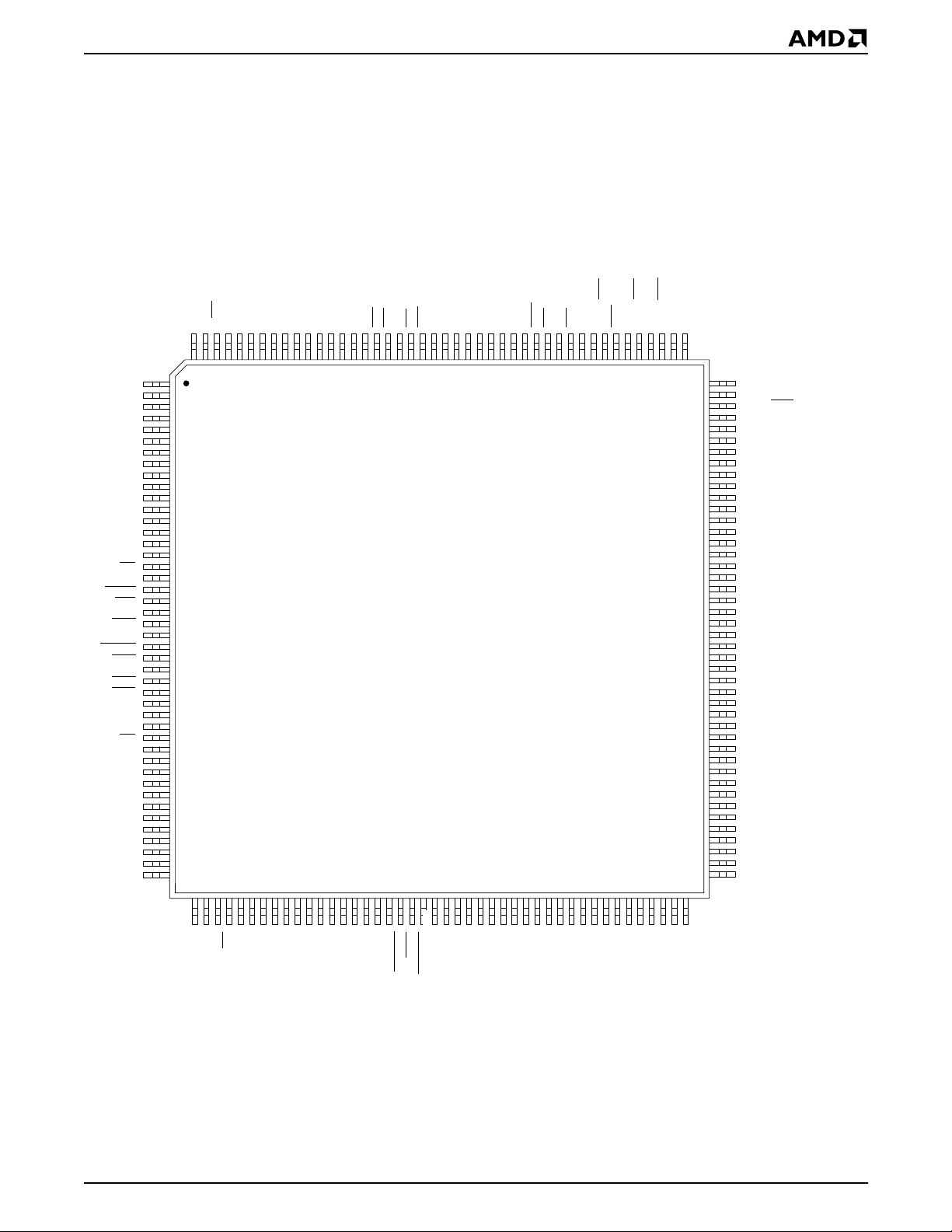
CONNECTION DIAGRAM (PQL176) Am79C973
NCNCC/BE3
AD24
AD25
VSSB
AD26
VDD_PCI
AD27
AD28
AD29
AD30
VSS
VSSB
AD31
VDD_PCI
REQ
GNT
CLK
RST
INTAPGVDD
TDI
VSSB
TDO
VDDB
TMS
TCK
RWU
176
175
174
173
172
171
170
169
168
167
166
165
164
163
162
161
160
159
158
157
156
155
154
153
152
151
150
149
148
147
NC
NC
IDSEL
AD23
VSSB
AD22
VDD_PCI
AD21
AD20
VDD
AD19
AD18
VSSB
AD17
VDD_PCI
AD16
C/BE2
VSS
FRAME
IRDY
VSSB
TRDY
VDD_PCI
DEVSEL
STOP
VDD
PERR
SERR
VSSB
PAR
VDD_PCI
C/BE1
AD15
VSS
AD14
AD13
VSSB
AD12
AD11
VDD_PCI
AD10
AD9
NC
NC
1
2
3
4
5
6
7
8
9
10
11
12
13
14
15
16
17
18
19
20
21
22
23
24
25
26
27
28
29
30
31
32
33
34
35
36
37
38
39
40
41
42
43
44
45464748495051525354555657585960616263646566676869707172737475767778798081828384858687
Am79C973
PQL176
146
WUMI
PME
145
VSS
144
EAR
143
EECS
142
VSSB
141
EESK/LED1/SFBD
LED2/MIIRXFRTGE
VDDB
XCLK/XTAL
VSSB
EED1/LED0NCNC
140
139
138
137
136
135
134
133
132
131
130
129
128
127
126
125
124
123
122
121
120
119
118
117
116
115
114
113
112
111
110
109
108
107
106
105
104
103
102
101
100
88
NC
NC
EEDO/LED3/MIIRXFRTGD
DVSSP
DVDDP
RXDVDDRX
RX+
SDIDVSSX
SDI+
TXDVDDTX
TX+
DVDDD
IREF
DVSSD
DVDDA
DVDDCO
XTAL1
XTAL2
VDDB
NC
VSSB
NC
VDD
NC
VSSB
VAUXDET
EBD0/RXD0
EBD1/RXD1
EBD2/RXD2
VSS
99
98
97
96
95
94
93
92
91
90
89
EBD3/RXD3
VDDB
EBD4/RX_DV
EBD5/RX_CLK
EBD6/RX_ER
VSSB
EBD7/TX_CLK
EBDA15/COL
EBDA14/CRS
NC
NC
NC
NC
AD8
AD7
VSSB
C/BE0
Pin 1 is marked for orientation.
AD6
AD5
VDD_PCI
VDD
AD4
AD3
AD2
VSSB
NC
AD1
AD0
VDD_PCI
VSS
EROMCS
EBWE
AS_EBOE
VSSB
EBCLK
EBUA_EBA0
VDD
VDDB
EBUA_EBA1
EBUA_EBA2
EBUA_EBA3
EBUA_EBA4
EBUA_EBA5/MDC
EBUA_EBA7/TX_ER
EBUA_EBA6/PHY_RST
VSS
VSSB
EBDA8/TXD0
VDDB
EBDA9/TXD1
EBDA10/TXD2
NC
EBDA11/TXD3
EBDA13/MDIO
EBDA12/TX_EN
Am79C973/Am79C975 19
21510D-3
Page 20
PRELIMINARY
CONNECTION DIAGRAM (PQR160) - Am79C975
C/BE3
AD24
AD25
VSSB
AD26
VDD_PCI
AD27
AD28
AD29
AD30
VSS
VSSB
AD31
VDD_PCI
REQ
GNT
CLK
RST
INTAPGVDD
TDI
VSSB
TDO
VDDB
TMS
TCK
RWU
WUMI
PME
160
159
158
157
156
155
154
153
152
151
150
149
148
147
146
145
144
143
142
141
140
139
138
137
136
135
134
133
132
IDSEL
AD23
VSSB
AD22
VDD_PCI
AD21
AD20
VDD
AD19
AD18
VSSB
AD17
VDD_PCI
AD16
C/BE2
VSS
FRAME
IRDY
VSSB
TRDY
VDD_PCI
DEVSEL
STOP
VDD
PERR
SERR
VSSB
PAR
VDD_PCI
C/BE1
AD15
VSS
AD14
AD13
VSSB
AD12
AD11
VDD_PCI
AD10
AD9
1
2
3
4
5
6
7
8
9
10
11
12
13
14
15
16
17
18
19
20
21
22
23
24
25
26
27
28
29
30
31
32
33
34
35
36
37
38
39
40
Am79C975
PQR160
414243444546474849505152535455565758596061626364656667686970717273747576777879
131
VSS
130
EAR
129
EECS
VSSB
EESK/LED1/SFBD
LED2/MIIRXFRTGE
128
127
126
125
VDDB
XCLK/XTAL
VSSB
124
123
122
EED1/LED0
121
120
119
118
117
116
115
114
113
112
111
110
109
108
107
106
105
104
103
102
101
100
99
98
97
96
95
94
93
92
91
90
89
88
87
86
85
84
83
82
81
80
EEDO/LED3/MIIRXFRTGD
DVSSP
DVDDP
RXDVDDRX
RX+
SDIDVSSX
SDI+
TXDVDDTX
TX+
DVDDD
IREF
DVSSD
DVDDA
DVDDCO
XTAL1
XTAL2
VDDB
MCLOCK
VSSB
MDATA
VDD
MIRQ
VSSB
VAUXDET
EBD0/RXD0
EBD1/RXD1
EBD2/RXD2
VSS
EBD3/RXD3
VDDB
EBD4/RX_DV
EBD5/RX_CLK
EBD6/RX_ER
VSSB
EBD7/TX_CLK
EBDA15/COL
EBDA14/CRS
AD8
AD7
AD6
AD5
AD4
AD3
AD2
AD1
AD0
VSSB
C/BE0
VDD_PCI
VDD
VSSB
VDD_PCI
VSS
EROMCS
EBWE
AS_EBOE
VSSB
EBCLK
EBUA_EBA0
VDD
VDDB
EBUA_EBA1
EBUA_EBA2
EBUA_EBA3
EBUA_EBA4
EBUA_EBA5/MDC
Pin 1 is marked for orientation.
20 Am79C973/Am79C975
VSS
VSSB
VDDB
EBDA8/TXD0
EBDA9/TXD1
EBDA10/TXD2
EBUA_EBA7/TX_ER
EBUA_EBA6/PHY_RST
EBDA11/TXD3
EBDA13/MDIO
EBDA12/TX_EN
21510D-4
Page 21
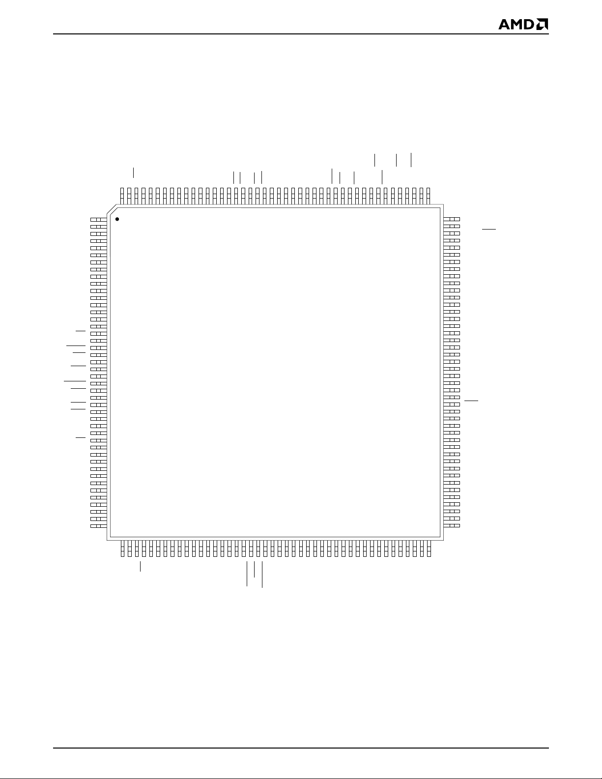
PRELIMINARY
CONNECTION DIAGRAM (PQL176) - Am79C975
NCNCC/BE3
AD24
AD25
VSSB
AD26
VDD_PCI
AD27
AD28
AD29
AD30
VSS
VSSB
AD31
VDD_PCI
REQ
GNT
CLK
RST
INTAPGVDD
TDI
VSSB
TDO
VDDB
TMS
TCK
RWU
WUMI
PME
176
175
174
173
172
171
170
169
168
167
166
165
164
163
162
161
160
159
158
157
156
155
154
153
152
151
150
149
148
147
146
NC
NC
IDSEL
AD23
VSSB
AD22
VDD_PCI
AD21
AD20
VDD
AD19
AD18
VSSB
AD17
VDD_PCI
AD16
C/BE2
VSS
FRAME
IRDY
VSSB
TRDY
VDD_PCI
DEVSEL
STOP
VDD
PERR
SERR
VSSB
PAR
VDD_PCI
C/BE1
AD15
VSS
AD14
AD13
VSSB
AD12
AD11
VDD_PCI
AD10
AD9
NC
NC
1
2
3
4
5
6
7
8
9
10
11
12
13
14
15
16
17
18
19
20
21
22
23
24
25
26
27
28
29
30
31
32
33
34
35
36
37
38
39
40
41
42
43
44
45464748495051525354555657585960616263646566676869707172737475767778798081828384858687
Am79C975
PQL176
145
VSS
144
EAR
143
EECS
142
VSSB
141
EESK/LED1/SFBD
LED2/MIIRXFRTGE
VDDB
XCLK/XTAL
VSSB
EED1/LED0NCNC
140
139
138
137
136
135
134
133
132
131
130
129
128
127
126
125
124
123
122
121
120
119
118
117
116
115
114
113
112
111
110
109
108
107
106
105
104
103
102
101
100
NC
NC
EEDO/LED3/MIIRXFRTGD
DVSSP
DVDDP
RXDVDDRX
RX+
SDIDVSSX
SDI+
TXDVDDTX
TX+
DVDDD
IREF
DVSSD
DVDDA
DVDDCO
XTAL1
XTAL2
VDDB
MCLOCK
VSSB
MDATA
VDD
MIRQ
VSSB
VAUXDET
EBD0/RXD0
EBD1/RXD1
EBD2/RXD2
VSS
99
98
97
96
95
94
93
92
91
90
89
88
EBD3/RXD3
VDDB
EBD4/RX_DV
EBD5/RX_CLK
EBD6/RX_ER
VSSB
EBD7/TX_CLK
EBDA15/COL
EBDA14/CRS
NC
NC
NC
NC
AD8
AD7
VSSB
C/BE0
Pin 1 is marked for orientation.
AD6
AD5
VDD_PCI
VDD
AD4
AD3
AD2
VSSB
NC
AD1
AD0
VDD_PCI
VSS
EROMCS
EBWE
AS_EBOE
VSSB
EBCLK
EBUA_EBA0
VDD
VDDB
EBUA_EBA1
EBUA_EBA2
EBUA_EBA3
EBUA_EBA4
EBUA_EBA5/MDC
EBUA_EBA7/TX_ER
EBUA_EBA6/PHY_RST
VSS
VSSB
EBDA8/TXD0
VDDB
EBDA9/TXD1
EBDA10/TXD2
NC
EBDA11/TXD3
EBDA13/MDIO
EBDA12/TX_EN
Am79C973/Am79C975 21
21510D-5
Page 22

PRELIMINARY
PIN DESIGNATIONS (PQR160) (Am79C973/Am79C975)
Listed By Pin Number
Pin
Pin
No.
Name
1 IDSEL 41 AD8 81 EBDA14/CRS 121 EEDI/LED0
2 AD23 42 C/BE0 82 EBDA15/COL 122 VSSB
3 VSSB 43 VSSB 83 EBD7/TX_CLK 123 XCLK/XTAL
4 AD22 44 AD7 84 VSSB 124 VDDB
5 VDD_PCI 45 VDD_PCI 85 EBD6/RX_ER 125 LED2
6 AD21 46 AD6 86 EBD5/RX_CLK 126 EESK/LED1
7 AD20 47 AD5 87 EBD4/RX_DV 127 VSSB
8 VDD 48 VDD 88 VDDB 128 EECS
9 AD19 49 AD4 89 EBD3/RXD3 129 EAR
10 AD18 50 AD3 90 VSS 130 VSS
11 VSSB 51 VSSB 91 EBD2/RXD2 131 PME
12 AD17 52 AD2 92 EBD1/RXD1 132 WUMI
13 VDD_PCI 53 VDD_PCI 93 EBD0/RXD0 133 RWU
14 AD16 54 AD1 94 VAUXDET 134 TCK
15 C/BE2 55 AD0 95 VSSB 135 TMS
16 VSS 56 VSS 96 MIRQ
17 FRAME
18 IRDY
19 VSSB 59 AS_EBOE
20 TRDY
21 VDD_PCI 61 EBUA_EBA0 101 VDDB 141 PG
22 DEVSEL 62 VSSB 102 XTAL2 142 INTA
23 STOP 63 EBUA_EBA1 103 XTAL1 143 RST
24 VDD 64 VDD 104 DVDDCO 144 CLK
25 PERR
26 SERR 66 EBUA_EBA2 106 DVSSD 146 REQ
27 VSSB 67 EBUA_EBA3 107 IREF 147 VDD_PCI
28 PAR 68 EBUA_EBA4 108 DVDDD 148 AD31
29 VDD_PCI 69 EBUA_EBA5/MDC 109 TX+ 149 VSSB
30 C/BE1
31 AD15 71 EBUA_EBA7/TX_ER 111 TX- 151 AD30
32 VSS 72 VSS 112 SDI+ 152 AD29
33 AD14 73 EBDA8/TXD0 113 DVSSX 153 AD28
34 AD13 74 VSSB 114 SDI- 154 AD27
35 VSSB 75 EBDA9/TXD1 115 RX+ 155 VDD_PCI
36 AD12 76 EBDA10/TXD2 116 DVDDRX 156 AD26
37 AD11 77 VDDB 117 RX- 157 VSSB
38 VDD_PCI 78 EBDA11/TXD3 118 DVDDP 158 AD25
39 AD10 79 EBDA12/TX_EN 119 DVSSP 159 AD24
40 AD9 80 EBDA13/MDIO 120
Note: For the Am79C973 controller, pins 96, 98, and 100 are no connects (NC).
Pin
No.
57 EROMCS 97 VDD 137 TDO
58 EBWE 98 MDATA (see Note) 138 VSSB
60 EBCLK 100 MCLOCK (see Note) 140 VDD
65 VDDB 105 DVDDA 145 GNT
70
Pin
Name
EBUA_EBA6/
PHY_RST
Pin
No.
99 VSSB 139 TDI
110 DVDDTX 150 VSS
Pin
Name Pin No.
(see Note) 136 VDDB
EEDO/LED3
MIIRXFRTGD
/
160 C/BE3
Pin
Name
/MIIRXFRTGE
/SFDB
22 Am79C973/Am79C975
Page 23

PRELIMINARY
PIN DESIGNATIONS (PQL176) (Am79C973/Am79C975)
Listed By Pin Number
Pin
Pin
No.
Name
1NC 45NC 89NC 133 NC
2NC 46NC 90NC 134 NC
3 IDSEL 47 AD8 91 EBDA14/CRS 135 EEDI/LED0
4 AD23 48 C/BE0 92 EBDA15/COL 136 VSSB
5 VSSB 49 VSSB 93 EBD7/TX_CLK 137 XCLK/XTAL
6 AD22 50 AD7 94 VSSB 138 VDDB
7 VDD_PCI 51 VDD_PCI 95 EBD6/RX_ER 139 LED2
8 AD21 52 AD6 96 EBD5/RX_CLK 140 EESK/LED1
9 AD20 53 AD5 97 EBD4/RX_DV 141 VSSB
10 VDD 54 VDD 98 VDDB 142 EECS
11 AD19 55 AD4 99 EBD3/RXD3 143 EAR
12 AD18 56 AD3 100 VSS 144 VSS
13 VSSB 57 VSSB 101 EBD2/RXD2 145 PME
14 AD17 58 AD2 102 EBD1/RXD1 146 WUMI
15 VDD_PCI 59 VDD_PCI 103 EBD0/RXD0 147 RWU
16 AD16 60 AD1 104 VAUXDET 148 TCK
17 C/BE2 61 AD0 105 VSSB 149 TMS
18 VSS 62 VSS 106 MIRQ
19 FRAME
20 IRDY
21 VSSB 65 AS_EBOE
22 TRDY
23 VDD_PCI 67 EBUA_EBA0 111 VDDB 155 PG
24 DEVSEL 68 VSSB 112 XTAL2 156 INTA
25 STOP 69 EBUA_EBA1 113 XTAL1 157 RST
26 VDD 70 VDD 114 DVDDCO 158 CLK
27 PERR
28 SERR 72 EBUA_EBA2 116 DVSSD 160 REQ
29 VSSB 73 EBUA_EBA3 117 IREF 161 VDD_PCI
30 PAR 74 EBUA_EBA4 118 DVDDD 162 AD31
31 VDD_PCI 75 EBUA_EBA5/MDC 119 TX+ 163 VSSB
32 C/BE1
33 AD15 77 EBUA_EBA7/TX_ER 121 TX- 165 AD30
34 VSS 78 VSS 122 SDI+ 166 AD29
35 AD14 79 EBDA8/TXD0 123 DVSSX 167 AD28
36 AD13 80 VSSB 124 SDI- 168 AD27
37 VSSB 81 EBDA9/TXD1 125 RX+ 169 VDD_PCI
38 AD12 82 EBDA10/TXD2 126 DVDDRX 170 AD26
39 AD11 83 VDDB 127 RX- 171 VSSB
40 VDD_PCI 84 EBDA11/TXD3 128 DVDDP 172 AD25
41 AD10 85 EBDA12/TX_EN 129 DVSSP 173 AD24
42 AD9 86 EBDA13/MDIO 130
43 NC 87 NC 131 NC 175 NC
44 NC 88 NC 132 NC 176 NC
Note: For the Am79C973 controller, pins 106, 108, and 110 are no connects (NC).
Pin
No.
63 EROMCS 107 VDD 151 TDO
64 EBWE 108 MDATA (see Note) 152 VSSB
66 EBCLK 110 MCLOCK (see Note) 154 VDD
71 VDDB 115 DVDDA 159 GNT
76
Pin
Name
EBUA_EBA6/
PHY_RST
Pin
No.
109 VSSB 153 TDI
120 DVDDTX 164 VSS
Pin
Name Pin No.
(see Note) 150 VDDB
EEDO/LED3
MIIRXFRTGD
/
174 C/BE3
Pin
Name
/MIIRXFRTGE
/SFDB
Am79C973/Am79C975 23
Page 24

PRELIMINARY
PIN DESIGNATIONS (PQR160, PQL176)
Listed By Group
Pin Name Pin Function Type
PCI Bus Interface
AD[31:0] Address/Data Bus IO TS3 32
C/BE[3:0] Bus Command/Byte Enable IO TS3 4
CLK Bus Clock I NA 1
DEVSEL Device Select IO STS6 1
FRAME Cycle Fram e IO STS6 1
GNT Bus Grant I NA 1
IDSEL Initialization Device Select I NA 1
INTA Interrupt O OD6 1
IRDY Initiator Ready IO STS6 1
PAR Parity IO TS3 1
PERR Parity Error IO STS6 1
REQ Bus Request O TS3 1
RST Reset I NA 1
SERR System Error O OD6 1
STOP Stop IO STS6 1
TRDY Target Ready IO STS6 1
Board Interface
LED0 LED0 O LED 1
LED1 LED1 O LED 1
LED2 LED2 O LED 1
LED3 LED3 O LED 1
XCLK External Clock Source Select I NA 1
XTAL Crystal Select I NA 1
XTAL1 Crystal Input -25 MHz Clock Reference I NA 1
XTAL2 Crystal Output O XTAL 1
EEPROM Interface
EECS Serial EEPROM Chip Select O O6 1
EEDI Serial EEPROM Data In O LED 1
EEDO Serial EEPROM Data Out I NA 1
EESK Serial EEPROM Clock IO LED 1
Expansion ROM Interface
AS_EBOE Address Strobe/Expansion Bus Output Enable O O6 1
EBCLK Expansion Bus Clock I NA 1
EBD[7:0] Expansion Bus Data [7:0] IO TS6 8
EBDA[15:8] Expansion Bus Data/Address [15:8] IO TS6 8
EBUA_EBA[7:0]
EBWE Expansion Bus Write Enable O O6 1
EROMCS Expansion Bus ROM Chip Select O O6 1
1. Not including test featu res
Expansion Bus Upper Addres s /Expansion Bus Addres s
[7:0]
1
O O6 8
Driver No. of Pins
24 Am79C973/Am79C975
Page 25
PRELIMINARY
PIN DESIGNATIONS
Listed By Group
Pin Name Pin Function Type
Physical Layer Interface (PHY)
IREF Internal Current Reference I NA 1
RX± Serial R eceive Data I NA 2
TX± Serial Transmit Data O NA 2
SDI± Signal Detect Input I NA 2
Powe r Mana gemen t Interface
RWU Remote Wake Up O O6 1
PME Power Management Event O OD6 1
WUMI Wake-Up Mode Indication O OD6 1
PG Power Good I NA 1
VAUXDET Auxiliar y Power Detect I NA 1
IEEE 1149.1 Test Access Port Interface (JTAG)
TCK Test Clock I NA 1
TDI Test Data In I NA 1
TDO Test Data Out O TS6 1
TMS Test Mode Select I NA 1
External Address Detection Interface (EADI)
EAR External Address Reject Low I NA 1
SFBD Start Frame Byte Delimiter O LED 1
MIIRXFRTGD MII Receive Frame Tag Data I NA 1
MIIRXFRTGE MII Receive Frame Tag Enable I NA 1
Media Independent Interface (MII)
COL Collision I NA 1
CRS Carrier Sense I NA 1
MDC Management Data Clock O OMII2 1
MDIO Management Data I/O I/O TSMII 1
RX_CLK Receive Clock I NA 1
RXD[3:0] Receive Data I NA 4
RX_DV Receive Data Valid I NA 1
RX_ER Receive Error I NA 1
TX_CLK Transmit Clock I NA 1
TXD[3:0] Transmit Data O OMII1 4
TX_EN Transmit Data Enable O OMII1 1
TX_ER Transmit Error O OMII1 1
Serial Management Interface (SMI) - Am79C975 only
MCLOCK SMI Clock I/O OD6 1
MDATA SMI Data I/O OD6 1
MIRQ SMI Interrupt O OD6 1
Note:
1. Not including test features.
1
Driver No. of Pins
Am79C973/Am79C975 25
Page 26
PRELIMINARY
PIN DESIGNATIONS
Listed by Group (Concluded)
Pin Name Pin Function Type
Power Supplies (MAC, PCI, Buffer, ROM)
VDD Digital Power P NA 6
VSS Digital Ground P NA 7
VDDB I/O Buffer Power P NA 6
VSSB I/O Buffer Ground P NA 17
VDD_PCI PCI I/O Buffer Power P NA 9
Power Suppli es (PHY)
DVDDA Analog PLL Power P NA 1
DVDDD, DVDDP Physical Data Transceiver (PDX) Power, IREF P NA 2
DVSSD, DVSSP Physical Data Transceiver (PDX) Ground P NA 2
DVDDTX, DVDDRX PHY I/O Buffer Power P NA 2
DVSSX PHY Ground P NA 1
DVDDCO Crystal Oscillator Power P NA 1
2
1
Driver No. of Pins
Notes:
1. Not including test features.
2. PHY power and ground pins require careful decoupling to ensure proper device performance.
26 Am79C973/Am79C975
Page 27
PIN DESIGNATIONS
PRELIMINARY
Listed By Driver Type
A sustained tri-state signal is a low active signal that is
driven high for one clock period before it is left floating.
The following table describes th e various type s of o utput drivers used in the Am79C973/Am79C975 controller. All I
and IOH v alues shown in the table apply to 3.3
OL
V signaling.
Name Type IOL (mA) IOH (mA) Load (pF)
LED LED 12 -0.4 50
OMII1 Totem Pole 4 -4 50
OMII2 Totem Pole 4 -4 390
O6 Totem Pole 6 -0.4 50
OD6 Open Drain 6 NA 50
STS6 Sustained Tri-State 6 -2 50
TS3 Tri-State 3 -2 50
TS6 Tri-State 6 -2 50
TSMII Tri-State 4 -4 470
TX is a differential output driver. Its characteristics and
those of X TAL2 output are des cribed in the DC Charac-
teristics sec ti on.
Am79C973/Am79C975 27
Page 28
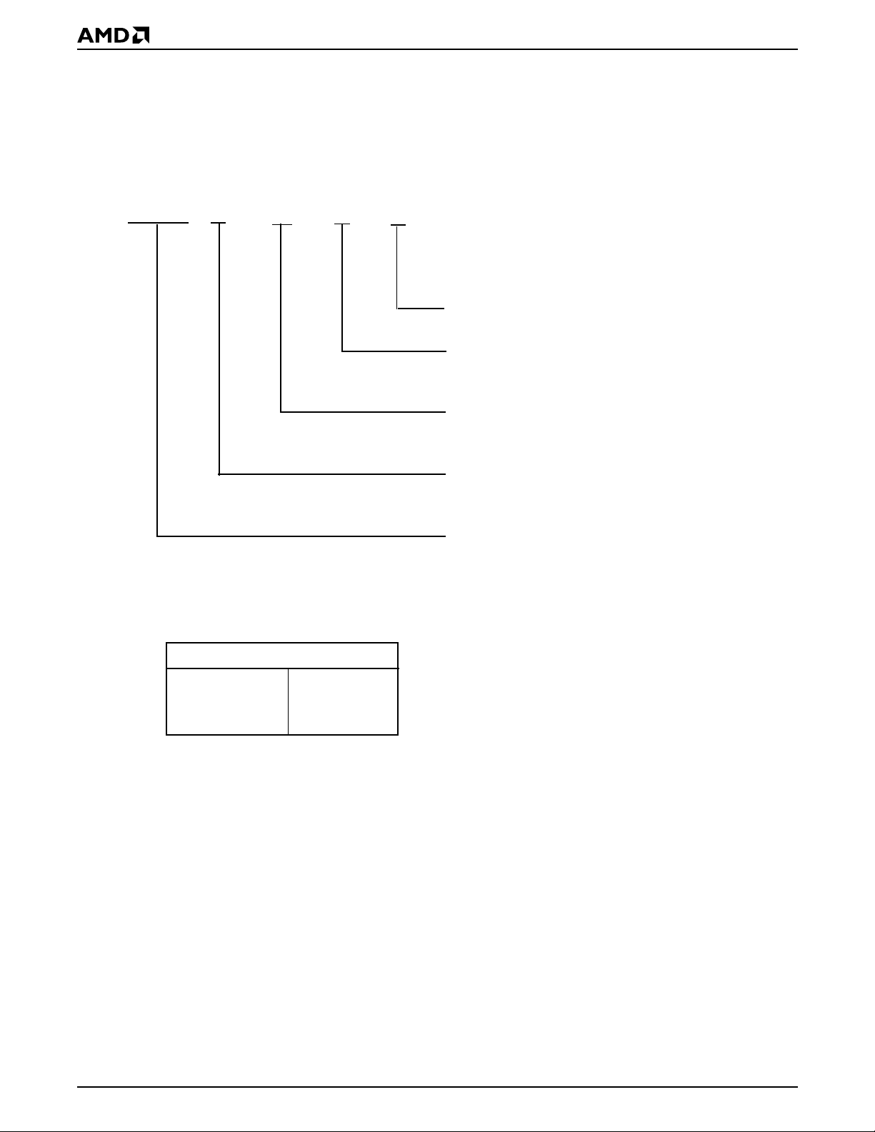
PRELIMINARY
ORDE RING INFORMATION
Standard Products
AMD standard produc ts are av ailable in sev eral pac kages and operating r anges. T he order number (Valid Combination) is formed
by a combination of the elements below.
AM79C973
AM79C975
K\V
C
\W
ALTERNATE PACKAGING OPTION
\W = Trimmed and formed in a tray
TEMPERATURE RANGE
C = Commercial (0° C to +70° C)
PACKAGE TYPE
K = Plastic Quad Flat Pack (PQR160)
V = Thin Quad Flat Pack (PQL176)
Valid Combinations
AM79C973,
AM79C975
KC\W,
VC\W
SPEED OPTION
Not applicable
DEVICE NUMBER/DESCRIPTION
Am79C973/Am79C975
Single-Chip 10/100 Mbps PCI Ethernet Cont roll er
with Integrated PHY
Valid Combinations
Valid Combinations list configurations planned to be
supported in volume for this device. Consult the local
AMD sales office to confirm availability of specific
valid combinations and to check on newly released
combinations.
28 Am79C973/Am79C975
Page 29

PRELIMINARY
PIN DESCRIPTIONS
PCI Interface
AD [31:0]
Add r e s s a n d Da ta Inpu t/Ou t p u t
Address and data are multiplexed on the same b us interface pins. During the first clock of a transaction, AD[31:0]
contain a physical addres s ( 32 bi ts) . During the subs equent clocks, AD[31:0] contain data. Byte ordering is little
endian by default. AD[7:0] are defined as the least significant byte (LSB) and AD[31:24] are defined as the most
significant byte (MSB). For FIFO data transfers, the
Am 79C973/Am 79C975 controller can be programm ed for
big e ndian byte or dering. See CSR3, bit 2 ( BSWP) for
more details.
Duri ng the address phase of the t r ansac t ion, when the
Am79C973/Am79C975 contr ol l er i s a bus master,
AD[31:2] wi ll address the active Double Word (DWor d).
The Am79C973/Am79C975 control l er al ways drives
AD[1:0] to ’00’ during the address phase indicating linear
burst order. When the Am 79C973/Am79C 975 controller is
not a bus master, t he AD[31: 0] l ines ar e cont inuously
monitor ed to determine if an addr ess match exi s t s f or
slave transfers.
Duri ng the data phase of t he trans action, AD[ 31:0] are
driven by the Am79C973/Am 79C975 controller when performing bus master write and slave read operations. Data
on AD[31:0] is latched by the Am79C 973/Am79C 975 contr oller when per for ming bus maste r read and slave writ e
operations.
When RST
testing.
C/BE[3:0]
Bus Co mman d a n d B y te En a ble s
Input/Output
Bus command and byte enables are multiplexed on the
same b us interface pins. During the address phase of the
tr ansact ion, C/ BE
the data phase, C/BE
byte enables define which physical byte lanes carry meaningful data. C/BE
applies to byte 3 (AD[31:24]). The function of the byte enables is independent of t he by te or de ring mode (BSWP,
CSR3, bit 2).
When RST
tes tin g .
CLK
Cloc k Inp ut
This clock is used to dri ve the system bus int erfac e and
the internal buffer management un it. All bus signals are
sampled on the rising edge of CLK and all parameters are
defi ne d wit h r espec t t o t hi s e dge. The Am79C973/
is ac tive, AD[ 31:0] ar e inputs f or NAND tree
[3: 0] define t he bus command. During
[3:0] are used as byte enables. The
0 applies to byte 0 (AD[7:0]) and C/BE3
is active, C/BE [3:0] are inputs for NAND tree
Am 79C975 controller normally operates over a frequency
range of 10 to 33 MHz on the PCI bus due to networking
demands. See the Frequency Demands for Network Op-
eration sect ion for det ail s. The Am79C973/Am79C975
contr oller wil l support a cl ock fr equency of 0 MHz after
certain precautions are taken to ensure data integrity. This
clock or a derivation is not used to drive any network functions.
When RST
ing .
is active, CLK is an input for NAND tree test-
DEVSEL
Device Select Input/
Output
The Am79C973/Am79C975 contr ol ler dr i ves DEVSEL
when it detects a transaction that selects the device as a
target. The device samples DEVSEL
claims a transaction that the Am79C 973/Am79C 975 controller has initiated.
When RST
tes tin g .
is activ e , DEVSEL is an input for NAND tree
to de tect if a target
FRAM E
Cy cle F r a me In p u t/Ou t p u t
FRAME is driven by the Am 79C973/Am79C 975 controller
when it is the bus master to indicate the beginning and durat ion of a t ransaction. FRAME
bus tr ansac tion i s beginning. FRAME
data transfers continue. FRAME
final dat a phase of a transac tion. When the Am79C973/
Am 79C975 controller is in slave m ode, it samples FRAME
to determine the address phase of a transaction.
Wh en RS T
tes tin g .
is active, FRAME is an inpu t fo r NAND tree
is as se rted t o indicate a
is as serted while
is deasserted before the
GNT
Bus Gra n t Inp u t
This signal indicates that the access to the bus has been
granted to the Am79C 973/Am79C 975 controller.
The Am 79C973/Am 79C975 controller supports bus parking. When the PCI bus is idle and the system arbiter asserts GNT
Am79C975 contr o ller, the devi c e will drive the AD[31:0],
C/BE
Wh en RST
ing .
without an active REQ from the Am79C973/
[3:0] and PA R lines.
is a ctiv e, GNT is an input for NAND tree test-
IDSEL
Initia liz a tio n D ev ic e Se le c t Inp u t
This signal is used as a chip select f or t he Am79C973/
Am 79C 975 controller during configuration read and write
transactions.
Wh en R ST
testing.
is acti ve, IDSEL is an input f or NAND tree
Am79C973/Am79C975 29
Page 30
PRELIMINARY
INTA
Interrupt Request Output
An attention signal which indicates that one or more of
the following status flags is set: EXDINT, IDON, MERR,
MISS, MFCO, MPINT, RCVCCO, RINT, SINT, TINT,
TXSTRT, UINT, MCCINT, MPDTINT, M APINT, MREINT, and STINT. Each status flag has either a ma sk or
an enable bit which allows for suppression of IN TA
as-
sertion. Table 1 shows the flag descriptions. By default
is an open-drain output. For applications that
INTA
need a high-active edge-se nsitive interrupt si gnal, the
pin can be configured for this mode by setting IN-
INTA
TLEVEL (BCR2, bit 7) to 1.
When RST is active, INTA is the output for NAND tree
testing.
IRDY
Initiator Ready Input/Output
IRDY indicates the ability of the initiator of the transac tion to complete the current data phase. IRDY
in conjunc ti o n w i t h T RDY
both IRDY
and TRDY are asserted simultaneously. A
. Wait states are inserted until
is used
data phase is completed on any clock when both IRDY
and TRDY are asserted.
When the Am79 C973/Am79C975 c ontroller is a bus
master, it asserts IRDY dur ing all wr ite d ata pha se s to
indicate that valid data is p resent on AD[31: 0]. Durin g
all read data phases, the device ass erts IRDY
to indi-
cate that it is ready to accept the data.
When the Am79C973/Am79C 975 controller is the tar-
get of a transaction, it checks IRDY
during all wri te data
phases to determine if valid data is present on
AD[31:0]. Durin g all read data phases, the device
checks IRDY
to determine if the initiator is ready to ac-
cept the data.
When RST is active, IRDY is an input for NAND tree
testing.
PAR
Parity Input/Output
Parity is even parity across AD[31:0 ] and C/BE[3:0].
When the Am79 C973/Am79C975 c ontroller is a bus
master, it generates parity during the address and write
data phases. It checks parity during read data phases.
When the Am79C973/Am79C975 controller operates
in slave mode, it checks parity during every address
phase. When it is the target of a cycle, it checks par ity
during write data phases and it generates parity during
read data phases.
When RST
testing.
is active, PAR is an input for NAND tre e
.
Table 1. Interrupt Flags
Name Description Mask Bit Interrupt Bit
EXDINT
IDON
MERR Memory Error CSR3, bit 11 CSR0, bit 11
MISS Missed Frame CSR3, bit 12 CSR0, bit 12
MFCO
MPINT
RCVCCO
RINT
SINT System Error CSR 5, bit 10 CSR5, bit 11
TINT
TXSTRT Transmit Start CSR4, bit 2 CSR4, bit 3
UINT User Interrupt CSR4, bit 7 CSR4, bit 6
MCCINT
MPDTINT
MAPINT
MREINT
STINT
Excessive
Deferral
Initialization
Done
Missed Frame
Count Overflow
Magic Packet
Interrupt
Receive
Collision Count
Overflow
Receive
Interrupt
Transmit
Interrupt
MII
Management
Command
Complete
Interrupt
MII PHY Detect
Transition
Interrupt
MII Auto-Poll
Interrupt
MII
Management
Frame Read
Error Interrupt
Software Timer
Interrupt
CSR5, bit 6 CSR5, bit 7
CSR3, bit 8 CSR0, bit 8
CSR4, bit 8 CSR4, bit 9
CSR5, bit 3 CSR5, bit 4
CSR4, bit 4 CSR4, bit 5
CSR3, bit 10 CSR0, bit 10
CSR3, bit 9 CSR0, bit 9
CSR7, bit 4 CSR7, bit 5
CSR7, bit 0 CSR7, bit 1
CSR7, bit 6 CSR7, bit 7
CSR7, bit 8 CSR7, bit 9
CSR7, bit 10 CSR7, bit 11
PERR
Parity Error Input/Output
During any slave write transaction and any master read
transaction, the Am79C973/Am79C975 controller asserts PERR
porting of the error is enabled by setting PERREN (PCI
Command register, bit 6) to 1. During any master write
transaction, the Am79C973/Am79C975 controller
monitors PERR
error.
When RST is active, PERR is an input for NAND tree
testing.
when it detects a data parity error and re-
to see if the target reports a data parity
30 Am79C973/Am79C975
Page 31

PRELIMINARY
REQ
Bus Request Input/Output
The Am79C973/Am79C975 controller asserts REQ
as a signal that it wishes to become a bus master. REQ
is driven high when the Am79C973/Am79C975 controller does not request the bus. In Power Management
mode, the REQ
When RST
testing.
pin will not be driven.
is active, REQ is an input for NAND tree
pin
RST
Reset Input
When RST is asser ted LOW and the PG pin is H IGH,
then the Am79C973/Am79C975 controller performs an
internal system reset of the type H_RESET
(HARDWARE_RESET, see section on RESET). RST
must be held for a minimum of 30 clock periods. While
in the H_RESET state, the Am79C973/Am79C975
controller will disable or deassert all outputs. RST
be asynchronous to clock when asser ted or deasserted.
When the PG pin is LOW, RST
pins except the PME
When RST
is enabled.
is LOW and PG is HIGH, NAND tree testing
pin.
disables all of the PCI
may
SERR
System Error Output
During any slave transaction, the Am79C973/
Am79C975 controller asserts SERR
address parity error, and reporting of the error is enabled by setting PERREN (PCI Command reg ister, bit
6) and SERREN (PCI Command register, bit 8) to 1.
By default SERR
nent test, it can be programmed to be an active-high
totem-pole output.
When RST
testing.
is an open-drain out put. For compo-
is active, SERR is an input for NAND tree
when it detects an
STOP
Stop Input/Out put
In slave mode, the Am79C973/Am79 C975 controller
drives the STOP
the current transaction. I n bus master mode, the
Am79C973/Am79C975 co ntroller c hecks STOP
termine if th e target wants to disc onnect the curren t
transaction.
When RST
testing.
signal to inform the bus master to stop
to de-
is active, STOP is an input for NAND tree
TRDY
Target Ready Input/Output
TRDY
indicates the ability of the tar get of the transaction to complete the current data phase. Wait states are
inserted until both IRD Y
taneously. A data phase is completed on any clock
when both IRDY
When the Am79 C973/Am79C975 c ontroller is a bus
master, it checks TRDY
determine if valid data is presen t on AD[31:0]. During
all write data phases, the device checks TRDY
mine if the target is ready to accept the data.
When the Am79C97 3/Am79C975 c ontroller is the target of a transaction, it asserts TRDY
data phases to indicate that valid data is present on
AD[31:0]. During all wr ite data phase s, the device asserts TRDY
data.
When RST is active, TRDY is an input for NAND tree
testing.
and TRDY are asserted.
to indicate that it is ready to accept the
and TRDY are asserted simul-
during all read da ta phases to
to deter-
during all read
PME
Power Management Event Output, Open Drain
PME is an output that can be used to indicate that a
power management event (a Magic Packet, an OnNow
pattern match , or a change in link state) has been detected. The PME
1. PME_STATUS and PME_EN are both 1, or
2. PME_EN_OVR and MPMAT are both 1, or
3. PME_EN_OVR and LCDET are both 1.
The PME
PCI clock.
signal is asynchronous with respect to the
pin is asserted when either
VAUXDET
Auxiliary Power Detect Input
VAUXDET is used to sense the presence of the auxi liary power and correctly report the capability of asserting PME
be connected to the auxiliary power supply or to ground
through a resistor. If PCI power is used to power the device, a pull-down resistor is requir ed. For system s tha t
provide auxiliary power, the VAUXDET pin should be
tied to auxiliary power through a pull-up resistor.
signal in D3 cold. The VAUXDET pin should
Board Interface
Note: Before programming the LED pins, see the
description of LEDPE in BCR2, bit 12.
LED0
LED0 Output
This output is designed to directly drive an LED. By default, LED0
can also be programmed to indicate other network sta-
indicates an active link connection. This pin
Am79C973/Am79C975 31
Page 32

PRELIMINARY
tus (see BCR4). The LED0 p in polar ity is pr ogrammable, but by default it is active LOW. When the LED0
polarity is programmed to active LOW, the output is an
open drain dr iver. When the LED0
grammed to active HIGH, the output is a totem pole
driver.
Note: The LED0
pin is multiplexed with the EEDI pin.
pin polarity is pro-
pin
LED1
LED1 Output
This output is designed to directly drive an LED. By default, LED1
This pin can also be programmed to indicate other network status (see BCR5). T he LED1
grammable, but by default, it is active LOW. When the
LED1
output is an open d rain driver. When the LED1
larity is pr ogrammed to active HIGH, th e output is a
totem pole driver.
Note: The LED1
SFBD pins.
The LED1
Detection to deter mine whe ther or not an EE PROM is
present at the Am79C97 3/Am79C975 controll er interface. At the last rising edge of CLK while RST
LOW, LED1
EEDET bit in BCR1 9. It is impor tant to ma intain adequate hold time around the rising edge of the CLK at
this time to ensure a c orrectly sampl ed value. A sampled HIGH value means that a n EEPROM is present,
and EEDET will be set to 1. A sampled LOW value
means that an EEPROM is not present, and EEDET
will be set to 0. See the EEPROM Auto-Detection sec-
tion for more details.
indicates receive activity on the network.
pin polarity is pro-
pin polarity is programmed to active LOW, the
pin po-
pin is multiplexed with the EESK and
pin is also used dur ing EEPROM Auto-
is active
is sampled to determine the value of the
LED3
LED3 Output
This output is designed to directly drive an LED. By defaul t, LED 3
This pin can also be programmed to indicate other network status (see BCR7). T he LED3
gramma ble, but by defaul t it is active LOW. When th e
LED3
output is an open drain driver. When the LED3
larity is pro grammed to active HIGH, the o utput is a
totem pole driver.
Special attention must be given to the external circuitry
attached to this pin. Whe n this pin is used to dri ve an
LED while an EEPROM is used in the system, then
buffering maybe required between the LED3
the LED circuit. If an LED circuit were directly attached
to this pin, it may create an I
not be met by the serial EEPROM attached to this pin.
If no EEPROM is included i n t he s y stem d es ign or low
current LEDs are used, then the LE D3
directly connected to an LED without buffering. For
more details regarding LED connection, see the section on LED Support.
Note: The LED3
MIIRXFRTGD pins.
indicates transmi t activity on the ne twork.
pin polarity is pro-
pin polarity is programmed to active LOW, the
pin po-
pin and
OL requirement that coul d
signal may be
pin is multiplexed with the EEDO and
PG
Power Good Input
The PG pin has two functions: (1) it puts the device into
Mag ic Packet™ mode, and (2) it blocks any resets
when the PCI bus power is off.
When PG is LOW and either MPPEN or MPMODE is
set to 1, the device enters the Magic Packet mode.
If no LED circuit is to be attached to this pin, then a pull
up or pull down resistor must be attached instead i n
order to resolve the EEDET setting.
WARNING
insured for correct EEPROM detection before the
deassertion of RST
: The input signal level of LED1 must be
.
When PG is LOW, a LO W assertion of the PCI RST
will only cause the PCI interface pins (except for PME
to be put in the high impedance state. The internal logic
will ignore the assertion of RST
When PG is HIGH, assertion of the PCI RST
causes the controller logic to be reset and the configuration information to be loaded from the EEPROM.
LED2
LED2 Output
This output is designed to directly drive an LED. This
pin can be programmed to indicate various network
status (see BCR6). T he L ED2
mable, but by default it is active LOW. When the LED2
pin polarity is programmed to active LOW, the output is
an open drain driver. When the LED2
grammed to active HIGH, the output is a totem pole
driver.
Note: The LED2
MIIRXFRTGE pin.
32 Am79C973/Am79C975
pin is multiplexed with the
pin polarity i s program-
pin polarity is pro-
PG input should be kept high during the NAND tree
testing.
RWU
Remote Wake Up Output
RWU is an output that is asserted either when the controller is in the Magic Packet mode and a Magic Packet
frame has been detected, or the controller is in the Link
Change Detect mode and a Link Change has been detected.
This pin can dr ive the external system mana gement
logic that causes the CP U to get out of a low power
pin
)
.
pin
Page 33

PRELIMINARY
mode of operation. This pin is implemented for designs
that do not support the PME
Three bits that are loaded from the EEP ROM into
CSR116 can program the characteristics of this pin:
1. RWU_POL determines the polarity of the RWU signal.
2. If RWU_GATE bit is set, RWU is forced to the high
impedance state when PG input is LOW.
3. RWU_DRIVER determines whether the output is
open drain or totem pole.
The internal power-on-reset signal forces this output
into the high impedance state until after the polarity and
drive type have been determined.
function.
WUMI
Wake-Up Mode Indicator Output
This output, which is cap able of drivi ng an LED, is asserted when the device is in Magic Packet mode. It can
be used to drive external logic that switches the device
power source from the main p ower supply to an aux iliary power supp l y.
EEPROM Interface
EECS
EEPROM Chip Select Output
This pin is designed to directly interface to a serial EEPROM that uses the 93C46 EEPROM interface protocol. EECS is connected to the EEPROM ’s chip select
pin. It is controlled by either the Am79C973/Am79C975
controller during command portions of a read of the entire EEPROM, or indir ectly by th e hos t syste m by wr iting to BCR19, bit 2.
EEDI
EEPROM Data In Output
This pin is designed to directly interface to a serial
EEPROM that uses the 93C46 EEPROM interface protocol. EEDI is connecte d to the EEPROM’s data input
pin. It is controlled by either the Am79C973/Am79C975
controller during command portions of a read of the entire EEPROM, or indirectly by the host system
by writing to BCR19, bit 0.
Note: The EEDI pin is multiplexed with the LED0
EEDO
EEPROM Data Out Input
This pin is designed to di rectly interface to a serial
EEPROM that uses the 93C46 EEPROM interface protocol. EEDO is connecte d to the EEPROM’s data output pin. It is controlled by either the Am79C973/
Am79C975Am79C973/Am79C975Am79C973/
Am79C975 controller during command portions of a
pin.
read of the entire EEPROM, or indirectly by the host
system by reading from BCR19, bit 0.
Note: The EEDO pin is multiplexed with the LED3
MIIRXFRTGD pins.
and
EESK
EEPROM Seria l Clock Output
This pin is designe d to directly interface to a serial
EEPROM that uses the 93C46 EEPROM interface protocol. EESK is connected to the EEPROM’s clock pin.
It is controlled by either the Am79C97 3/Am79C975
controller directly during a read of the entire EEPROM,
or indirectly by the host system by writing to BCR19, bit
1.
Note: The EESK pin is multiplexed with the LED1
SFBD pins.
The EESK pin is also used during EEPROM AutoDetection to deter mine whe ther or not an EEPROM is
present at the Am79C97 3/Am79C975 controll er interface. At the rising edge of the last CLK edge while RST
is asserted, EESK is sampled to determine the value of
the EEDET bit in BCR19. A sampled HIGH value
means that an EEPROM is present, and EEDET will be
set to 1. A sampled LOW value means that an EEPROM is not present, and EEDET will be set to 0. See
the EEPROM Auto-Detection section for more details.
If no LED circuit is to be attached to this pin, then a pull
up or pull down resistor must be attached instead to resolve the EEDET setting.
WARNING
valid for correct EEPROM detection before the
deassertion of RST
: The input signal level of EESK must be
.
and
Expansion Bus Interface
EBUA_EBA[7:0]
Expansion Bus Upper Address/
Expansion Bus Address [7:0] Output
The EBUA_EBA[7:0] pins provide the least and most
significant bytes of address on the Expansion Bus. The
most significant address byte (address bits [19:16] during boot device accesses) is valid on these pins at th e
beginning of a boot device access, at the rising edge of
AS_EBOE
ternally in a D fli p-flop. During subseq uent cycles of a
boot device access, addres s bits [7:0] are p resent on
these pin s.
All EBUA_EBA[7:0] outputs are forced to a constant
level to conserve power while no access on the Expansion Bus is being performed.
Note: EBUA_EBA[7:5] pins are multiplexed with the
TX_ER, PHY_RST, and MDC pins.
. This upper address byte must be stored ex-
Am79C973/Am79C975 33
Page 34

PRELIMINARY
EBDA[15:8]
Expansion Bus Data/Address [15:8] Input/
Output
When EROMCS is asserted low, EBDA[15:8] contain
address bits [15:8] for boot device accesses.
The EBDA[15:8] signals are driven to a constant level
to conserve power while no access on the Expansion
Bus is being performed.
Note: EBDA[15:8] pins are multiplexed with the
TXD[3:0], TX_EN, MDIO, CRS, and COL pins.
EBD[7:0]
Expansion Bus Data [7:0] Input/Output
The EBD[7:0] pins provide data bit s [7:0] for EPROM/
FLASH accesses. The EBD[ 7:0] signals are internally
forced to a constant level to conserve power while no
access on the Expansion Bus is being performed.
Note: EBD[7:0] pins are multiplexed with the
RXD[3:0], RX_DV, RX_CLK, RX_ER, and TX_CLK
pins.
EROMCS
Expansion ROM Chip Select Output
EROMCS serves as the chip select for the boot device.
It is asserted low during the data phases of boot device
accesses.
AS_EBOE
Address Strobe/Expansion Bus
Output Enable Output
AS_EBOE
upper address bits on the EBUA_EBA[7:0] pins and as
the output enable for the Expansion Bus.
As an address strobe, a rising edge on AS_EBOE
supplied at the beginning of boot device accesses. This
rising edge provides a clock edge for a ‘374 D-type
edge-triggered flip-flop which must store the upper address byte during Expa nsion Bus accesses for
EPROM/Flash.
AS_EBOE
read operations on the expansion bus and is deasserted during boot device write operations.
functions as the address strobe for the
is
is asserted active LOW during boot device
EBWE
Expansion Bus Write Enable Output
EBWE provides the wr ite enable for writ e accesse s to
the Flash device.
EBCLK
Expansion Bus Clock Input
EBCLK may be used as the fundamental clock to drive
the Expansion Bus and inte rn al SRAM a ccess cy cles.
The actual inter nal clock used to dr ive the Expansion
Bus cycles depends o n the values of the EBCS and
CLK_F A C settings in BCR27. Refer to the SRAM Interface Bandwidth Requirements section for details on determining the requ ired EBCLK frequency. If a clock
source other than the EBCLK pin is programmed
(BCR27, bits 5:3) to be used to run the Expansion Bus
interface, this input should be tied to VDD through a 4.7
kW resistor.
EBCLK is not used to drive the bus interface, inter nal
buffer management unit, or the network functions.
Media Independent Interface (MII)
TX_CLK
Transmit Clock Input
TX_CLK is a conti nuous clock input th at provides the
timing reference for the transfer of the TX_EN,
TXD[3:0], and TX_ER signals out of the Am79C973/
Am79C975 device. TX_CLK must provide a nibble rate
clock (25% of the network da ta rate). Hence, an MII
transceiver operating at 10 Mbps must provide a
TX_CLK frequency of 2 .5 MHz and an MII transc eiver
operating at 100 Mbps must provide a TX_CLK frequency of 25 MHz.
Note: The TX_CLK pin is multiplexed with the EBD7
pin.
TXD[3:0]
Transmit Data Output
TXD[3:0] is the nibble-wide MII transmit data bus. V alid
data is generated on TXD[3:0] on every TX_CLK rising
edge while TX_EN is asserted. While TX_EN is deasserted , TXD[3:0] values are dri ven to a 0. TXD[3:0]
transitions synchronous to TX_CLK rising edges.
Note: The TXD[3:0] pins are multiplexed with the
EBDA[11:8] pins.
TX_EN
Transmit Enable Output
TX_EN indicates when the Am79C973/Am79C975 device is presenting valid transmit nibbles on the MII.
While TX_EN is asser ted, the Am79C9 73/Am79C975
device generates TXD[3:0] and TX_ER on TX_CLK rising edges. TX_EN is asserted with the first nibble of
preamble and remains asserted throughout the duration of a packet until it is deasserted prior to the first
TX_CLK following the final nibble of the frame. TX_EN
transitions synchronous to TX_CLK rising edges.
Note: The TX_EN pin is multiplexed with the EBDA12
pin.
TX_ER
Transmit Error Output
TX_ER is an out put th at, if asserted wh ile TX _EN is asserted, i nstructs the MII PHY device connecte d to the
Am79C973/Am79C975 device to transm it a code
34 Am79C973/Am79C975
Page 35

PRELIMINARY
group error. TX_ER is unused and is reserved for future
use and will always be driven to a logical zero.
Note: The TX_ER pin is multiplexed with the
EBUA_EBA7 pin.
COL
Collision Input
COL is an input that indicates that a collision has been
detected on the network medium.
Note: The COL pin is multiplexed with the EBDA15
pin.
CRS
Carrier Sense Input
CRS is an input that indicates that a non-idl e medium,
due either to transmit or receive activi ty, has been detected.
Note: The CRS pin is multiplexed with the EBDA14
pin.
RX_ER
Receive Error Input
RX_ER is an input that indicates that the MII transceiver device has detected a coding error in the receive
frame currently being transferred on the RXD[3:0] pins.
When RX_ER is asser t ed while RX_DV is asser ted, a
CRC error will be indicated in the receive descriptor for
the incoming receive frame. RX_ER is ignored while
RX_DV is deasserted. Spec i al co de group s gen erate d
on RXD while RX_DV is deasserted are ignor ed (e.g.,
Bad SSD in TX and IDLE in T4). RX_ER transitions are
synchronous to RX_CLK rising edges.
Note: The RX_ER pin is multiplexed with the EBD6
pin.
MDC
Management Data Clock Output
MDC is a non-continuous clock output t hat provides a
timing referenc e for bits on the MDIO p in. Duri ng MII
management por t operations, MDC runs at a nominal
frequency of 2.5 MHz. When no management operations are in progress, MDC is driven LOW. The MDC is
derived from the Time Base Clock.
If the MII port is not selected, th e MDC pin can be left
floating.
Note: The MDC pin is multiplexed with the
EBUA_EBD5 pin.
MDIO
Management Data I/O Input/Output
MDIO is the bidirectional M II management por t data
pin. MDIO is an output during the header portion of the
management frame transfers and durin g the data portions of write transfers. MDIO is an input during the
data portions of read data transfers. When an operation
is not in progress on the management port, MDIO is not
driven. MDIO transitions from the Am79C973/
Am79C975 contro ller are sync hronous to MDC falling
edges.
If the PHY is attached through an MII physical connector, then the MDIO pin should be externally pulled down
SS with a 10-kΩ ±5% resistor. If the PHY is on
to V
board, then the MDIO pin should be externally pulled
up to V
Note: The MDIO pin is multiplexed with the EBDA13
pin.
CC with a 10-kΩ ±5% resistor.
PHY_RST
Physical Layer Reset Output
PHY_RST is an output pin that is used to reset an external PHY. This output eliminates the need for a fan
out buffer for the PCI RST signal, provides polarity for
the specific external PHY used, and prevents the resetting of the external PHY when the PG input is LOW.
The output polarity is determined by RST_POL bit
(CSR 116, bit 0).
Note: The PHY_RST pin is multiplexed with the
EBUA_EBA6 pin.
RX_CLK
Receive Clock Input
RX_CLK is a clock input that provides the timing reference for the transfer of the RX_DV, RXD[3:0], and
RX_ER signals into the Am79C973/Am79C975 device.
RX_CLK must provide a nibble rate clo ck (25% of the
network data rate). Hence, when the Am79C973/
Am79C975 device is operatin g a t 10 Mbp s, it p rovides
an RX_CLK frequency o f 2. 5 M H z, an d at 10 0 M bps i t
provides an RX_CLK frequency of 25 MHz.
Note: The RX_CLK pin is multip lexed with the EBD5
pin.
RXD[3:0]
Receive Data Input
RXD[3:0] is th e nibble-wide MII-compa tible receive
data bus. Data on RXD[3:0] is sampled on every rising
edge of RX_CLK while RX_D V is asserted. RXD[3:0] is
ignored while RX_DV is de-asserted.
Note: The RXD[3:0] pin is multiplexed with the
EBD[3:0] pins.
RX_DV
Receive Data Valid Input
RX_DV is an input used to indicate tha t valid received
data is being presented o n the RXD[3:0] pins and
RX_CLK is synchronous to the receive data. In order
for a frame to be fully received by the Am79C973/
Am79C975 device, RX_DV must be asserted prior to
the RX_CLK rising edge, when the first nibble of the
Am79C973/Am79C975 35
Page 36

PRELIMINARY
Start of Frame Delimiter is driven on RXD[3:0], and
must remain asserted until after the rising edge of
RX_CLK, when the last nibble of the CRC is dr i ven on
RXD[3:0]. RX_DV must then be deasserted prior to the
RX_CLK rising edge which follows this final nibble.
RX_DV transitions are synchronous to RX_CLK r ising
edges.
Note: The RX_DV pin is multiplexed with the
EBD4 pin.
External Address Detection Interface
EAR
External Address Reject Low Input
The incoming frame will be che cked against the internally active address detection mechanisms and the result of this check will be OR’d with the value on the EAR
pin. The EAR pin is defined as REJECT. The pin value
is OR’d with the internal address detection result to determine if the current frame sho uld be ac cepted or rejected.
The EAR
be tied to VDD through a 10-k
When RST
testing.
SFBD
Start Frame-Byte Delimiter Output
An initial rising edge on the SFBD signal indicates that
a start of valid data is present on the RXD[3:0] pins.
SFBD will go high f or one ni bb le ti me (400 ns when operating at 10 Mbps and 40 ns when operating at 100
Mbps) one RX_CLK period after RX_ DV has been asserted and RX_ER is deasserted and t he detecti on of
the SFD (Start of Frame Delimiter) of a received frame.
Data on the RXD[3:0] will be the start of the destination
address field. SFBD will subsequently toggle every nibble time (1.25 MHz frequency when operating at 10
Mbps and 12.5 MHz fr equenc y when o perating at 10 0
Mbps) indicating the first nibble of each subsequent
byte of the received nibble stream. The RX_CLK
should be used in con junction with the S FBD to latch
the correct data for external address matching. SFBD
will be active only during frame reception.
Note: The SFBD pin is multiplexed with the EESK and
LED1
MIIRXFRTGD
MII Receive Frame Tag Enable Input
When the EADI is enabled (EADISEL, BCR2, bit 3), the
Receive Frame Tagging i s enabled (RXFRTG, CSR7,
bit 14), and the MII Snoop mode is selected, the MIIRXFRTGD pin becomes a data input pin for the Receive
Frame Tag. See the Receive Fr ame Tagging section for
details.
pin must not be left unconnecte d, it should
Ω ±5% resistor.
is active, EAR is an input for NAND tree
pins.
Note: The MIIRXFRTGD pin is multiplexed with the
EEDO and LED3
pins.
MIIRXFRTGE
MII Receive Frame Tag Enable Input
When the EADI is enabled (EADISEL, BCR2, bit 3), the
Receive Frame Tagging is enabled (RXFRTG, CSR7,
bit 14), and the MII Snoop mode is selected, the MIIRXFRTGE pin becomes a data input enable pin for the Receive Frame Tag. See the Receive Frame Tagging
section for details.
Note: The MIIRXFRTGE pin is multiplexed with the
pin.
LED2
IEEE 1149.1 (1990) Test Access Port
Interface
TCK
Test Clock Input
TCK is the clock input for the boundary scan test mode
operation. It can operate at a frequency of up to 10
MHz. TCK has an internal pull up resistor.
TDI
Test Data In Input
TDI is the test data input path to the Am79C973/
Am79C975 controller. The pin has an internal pull up
resistor.
TDO
Test Data Out Output
TDO is the test data ou tput path from t he Am79C973 /
Am79C975 controller. The pin is tri-stated when the
JTAG port is inactive.
TMS
Test Mode Select Input
A serial input bit stre am on the TMS pin is used to define the speci fic boundary scan test to be executed.
The pin has an internal pull up resistor.
Network Interfaces
TX+, TXSerial Transmit Data
MLT-3/PECL Output
These pins are the 10BA SE-T/100BA SE-X differential
drivers. For 100BASE-FX, these transmit outputs carry
differential PECL-level NRZI data for direct connectio n
to an external fiber optic transceiver. They can be
forced to logical 0 (TX+ low, TX- high) by programming
the TX_DISABLE bit (bit 3 of the internal PHY Control/
Status Register, Register 17). For 100BASE-TX, these
pins carry ML T-3 data and are connected to the primary
side of the magnetics m odule. For 10BASE-T, these
36 Am79C973/Am79C975
Page 37

PRELIMINARY
pins carr y the transmi t output data and are connecte d
to the transmit side of the magnetics module.
RX+, RXSerial Receive Data
MLT-3/PECL Input
These pins are the 10BASE-T/10 0BASE-X por t differential receiver pairs. They receive MLT-3 data and are
connected to the receive side of the magnetics module
in 100BASE-TX operation. They receive PECL NRZI
data from an external fiber optic transceiver in
100BASE-FX appl ication. For 10BASE-T, these pins
accept the receive input data from the magnetics module.
SDI+, SDISignal Detect Input
These pins control the se lection between PECL and
MLT-3 data for the TX± and RX ± pins. For 100BASETX or 10BASE-T, both of these pins may be tied to
ground or left floating. This enables transmission and
reception of MLT-3 or 10BASE-T signals at the TX± and
RX± pins. For 100BASE-FX, the se pins are bia sed at
PECL levels. They are connected to the SDI pin from
the optical transceiver modu le to indicate whe ther the
received signal is above the requ ired threshol d. If signal detect is not available, these pins should be tied to
a PECL logical 1 (SDI+ = PECL 1, SDI- = PECL 0). See
Table 2.
Table 2. SDI± Settings for Transceiver Operation
SDI+ SDI- Port Mode
TTL LOW
(<0.8 V)
TTL HIGH
(>2.0 V)
TTL LOW
(<0.8 V)
TTL HIGH
(>2.0 V)
MLT-3/10BASE-T
Mode
PECL Mode
IREF
Internal Current Reference Input
This pin serves as a current reference for the integrated
10/100 PHY. It must be connected to ground via a
Ω resistor (1%).
12 k
Clock Interface
XTAL1
Crystal Input Input
The internal clock generat or uses a 25-MHz (50 ppm100 ppm) crystal that is attached to the XTAL1 and
XTAL2 pins. XTAL1 may alternatively be driven using
an external 25 MHz (50 p pm - 100 ppm) CMOS-level
clock signal when XT AL2 is left floating. The XT AL1 pin
is not 5 V tolerant and must o nly be dr iven by a 3.3 V
clock source.
XTAL2
Crystal Output Output
The internal cl ock generator uses a 2 5 MHz (50 ppm 100 ppm) crystal that is attached to the pins XTAL1 and
XTAL2. XTAL1 may alternatively be driven using an external 25 MH z (50 ppm - 100 ppm ) CMOS-level clock
signal when XTAL2 is left floating.
XCLK/XTAL
External Clock/Crystal Select Input
When HIGH, an External Clock Source is s el ected bypassing the Crystal circuit. When LOW, a Crystal is
used instead. The following table illustrates how this pin
works.
Output
Input Pin
XATL1 XTAL2 0 Crystal
XTAL1 Don’t Care 1
Pin XCLK/XTAL Clock Source
Oscillator/
External CLK
Source
Serial Management Interface (SMI)
(Am79C975 only)
MCLOCK
SMI Clock Input/Output
MCLOCK is the clock pin of the serial management interface. MCLOCK is typically driven by an external I
SMBus master. The Am79C975 controller will drive the
clock line low in order to insert wait states before it
starts se ndi ng out d ata i n res po ns e to a read. T h e frequency of the clock signal can vary between 10 kHz
and 100 kHz, and it can change from cycle to cycle.
Note: MCLOCK is also capable of running at a frequency as high as 2.5 MHz to allow for shorter production test time.
MDATA
SMI Data Input/Output
MDATA is the data pin of the serial man age men t i nterface. MDATA can be driven by an external I
master or by the Am79C975 controller. The interface
protocol defines exactly at what time the Am79C975
controller has to listen to the MDATA pin and at what
time the controller must drive the pin.
2
MIRQ
SMI Interrupt Output
MIRQ is an asynchronous attention signal that the
Am79C975 controll er provides to indicate that a m anagement frame has been transm it ted or r eceived. Th e
assertion of the MIRQ
bal mask bit (MIRQEN) or individual mask bits
signal can be controlled by a glo-
2
C/
C/SMBus
Am79C973/Am79C975 37
Page 38

PRELIMINARY
(MRX_DONEM, MTX_DONEM) located in the Command register.
Note: The SMI interru pt acknowledge d oes n ot follow
the SMBus aler t protocol, but simply requires clearing
the interrupt bit.
Power Supply
VDDB
I/O Buffer Power (6 Pins) +3.3 V Power
There are seven power supply pins that are used by the
input/output buffer drivers. All VDDB pins must be connected to a +3.3 V supply.
VDD_PCI
PCI I/O Buffer Power (9 Pins) +3.3 V Power
There are nine power supply pins tha t ar e us ed by the
PCI input/output buffer drivers (except PME
VDD_PCI pins must be connected to a +3.3 V supply.
VSSB
I/O Buffer Ground (17 Pins)
Ground
There are 17 ground pins that are used by the input/
output buffer drivers.
VDD
Digital Power (6 Pins) +3.3 V Power
There are six power supply pins that are used by the internal digital cir cu itry. All VDD pins must be connected
to a +3.3 V supply.
VSS
Digital Ground (8 Pins) Ground
There are eight ground pins that are use d by the internal digital circuitry.
driver). All
DVDDD, DVDDP
PDX Block Power +3.3 V Power
These pins supply power to the 100 Mbps Physical
Data Transceiver (PDX) block. They must be connected to a +3.3 V ±5% source. These pins require
careful decoupling to ensure proper device performance.
DVDDRX, DVDDTX
I/O Buffer Power +3.3 V Power
These pins supply power to the MLT-3/PECL/10BASET input/output buffers. They also supply the MLT-3 circuits (equalizer, etc.) of the network port. They must be
connected to a +3.3 V ±5% source. These pins require
careful decoupling to ensure proper device performance.
DVDDA
Analog PLL Power +3.3 V Power
This pin supplies power to the IRE F current reference
circuit and the 10BASE-T analog PLL. They must be
connected to a +3.3 V ±5% source. These pins require
careful decoupling to ensure proper device performance.
DVSSX
All Blocks Ground
These pins are the gro und conn ection for all blocks of
the dev ice e xce pt the P DX b loc k. The y m ust be directl y
connected to the common external ground plane.
DVSSD, DVSSP
PDX Ground Ground
These pins are the ground co nnecti on for the Physical
Data Transceiver (PDX) block. They must be directly
connected to the common external ground plane.
DVDDCO
Crystal +3.3 V Power
This pin supplies the power to the Crystal circuit.
38 Am79C973/Am79C975
Page 39

PRELIMINARY
BASIC FUNCTIONS
System Bus Interface
The Am79C973/Am79C975 controllers are designed
to operate as a bus master during nor mal operations.
Some slave I/O accesses to the Am79C973/
Am79C975 controllers are required in normal operations as well. Initialization of the Am79C973/
Am79C975 controllers are ac hieved through a combination of PCI Configuration Space accesses, bus slave
accesses, bus master acces ses, and an opti onal rea d
of a serial EEPROM that is performed by the
Am79C973/Am79C975 controllers. The EEPROM
read operation is performed through the 93C46 EEPROM interface. The ISO 8802-3 (IEEE/ANSI 802.3)
Ethernet Address may reside within the serial EEPROM. Some Am79C973/Am79C975 controller configuration registers may also be programmed by the
EEPROM read operation.
The Address PROM, on-chip bo ard-configuration registers, and the Ether net contr oller register s occupy 32
bytes of address space. I/O an d memor y mapped I/O
accesses are supported. Base Address registers in the
PCI configuration sp ace allow locating the address
space on a wide variety of starting addresses.
For diskless stations, the Am79C973 /Am79C975 co ntrollers support a ROM or Flash-based (both referred to
as the Expansion ROM throughout this specification)
boot device of up to 1 Mbyte in size. The host can map
the boot device to any memory address that aligns to a
1-Mbyte boundary by modifying the Expansion ROM
Base Address register in the PCI configuration space.
Software Interface
The software interface to the Am79C973/Am79C975
controllers are divide d in to thr ee parts. One part is the
PCI configuration registers used to identify the
Am79C973/Am79C975 controllers and to s etup the
configurat ion of the device. The s etup informat ion includes the I/O or memory mapped I/O base address,
mapping of the Expansion ROM, and the routing of the
Am79C973/Am79C975 co ntroller interrupt channel .
This allows for a jumperless implementation.
The second por tion of the software interface is the d irect access to the I/O resources of the Am79C973/
Am79C975 control lers. The Am79C973/Am79C 975
controllers occupy 32 bytes of address space that must
begin on a 32-byte block boundary . The address space
can be mapped into I/O or memory space (memory
mapped I/O). The I/O Base Address Register in the
PCI Configuration Space controls the s tar t address o f
the address space if it is mapped to I/O space. The
Memory Mapped I/O Base Address Register controls
the start addres s of the address space if it is mapped
to memory space. The 32-byte address space is used
by the so f tware to pr ogram the Am 79 C 97 3 /Am 79 C 9 75
controller operating mode, to enable and disable various features, to monitor operating status, and to request particular functions to be executed by the
Am79C973/Am79C975 controllers.
The third por tion of th e software interface is the d escriptor and buffer areas that are shared between the
software and the Am79C973/Am79C975 controllers
during normal network operations. The descriptor area
boundaries are se t by the so ft ware an d do not ch ang e
during normal network operations. There is one descriptor area for receive activity and there is a separate
area for transmit activity . The descriptor space contains
relocatable pointers to the network frame data, and it is
used to transfer frame status from the Am79C973/
Am79C975 controllers to the software. The buffer
areas are locati ons that hold frame da ta for transmission or that accept frame data that has been received.
Network Interfaces
The Am79C973/Am79C975 controllers provide all of
the PHY layer functions for 10 Mb ps (10BASE-T) or
100 Mbps (100BASE-TX). It also provides a Pseudo
ECL (PECL) interface for 100BASE-FX fiber networks.
The Am79C973 /Am79C975 con trollers suppor t both
half-duplex and full-duplex operation on ne twork inter faces.
Serial Management Interface
(Am79C975)
The Am79C975 controller provi des a 3-pin int erface
based on the I
system to monitor the status of the system hardware
and report the results to the management station or
system administrator. Monitored information may include critical system parameters, such as voltage, temperature, and fan speed, as well as system
management events, such as chassis intrusion, operating system errors and power-on failures.
2
C and SMBus standards that enables a
MII Interface
The Am79C973/Am79C975 supports an MII interface
mode that makes the device operate like a
PCnet-FAST+ device. The MII pins are multiplexed with
the expansion bus pins, which means the device will
only support either an EPROM/Flash or an external
PHY but not both. To enter this mode, set PHYSELEN
(BCR2, bit 13) = 1 and PHYSEL (BCR18, bit 4 and
bit 3) = 10. This mode isolates the internal PHY to allow
interface with an external PHY . For a more detailed description of the M II inte rface including timing diagrams
see Appendix C. Refer to the connection diagram to
see how the pins are multiplexed.
Am79C973/Am79C975 39
Page 40

PRELIMINARY
DETA ILED FUNC TIONS
Slave Bus Interface Unit
The slave bus interface unit (BIU) controls all accesses
to the PCI configuration space, the Control and Sta tus
Registers (CSR), the Bu s Configuration Registers
(BCR), the Ad dress PROM (APROM) lo cations, and
the Expansion ROM. Table 3 shows the response of
the Am79C973/Am79C975 controllers to each of the
PCI commands in slave mode.
Table 3. Slave Commands
C[3:0] Command Use
0000
0001 Special Cycle Not used
0010 I/O Read
0011 I/O Write
0100 Reserved
0101 Reserved
0110 Memory Read
0111 Memory Write
1000 Reserved
1001 Reserved
1010
1011
Interrupt
Acknowledge
Configuration
Read
Configuration
Write
Not used
Read of CSR, BCR, APROM,
and Reset registers
Write to CSR, BCR, and
APROM
Memory mapped I/O read of
CSR, BCR, APROM, and
Reset registers
Read of the Expansion Bus
Memory mapped I/O write of
CSR, BCR, and APROM
Read of the Configuration
Space
Write to the Configuration
Space
configuration cycle. AD[7:2] se lect the DWord location
in the configuration space. The Am79C973/Am79C975
controllers ignore AD[10:8], because it is a single function device. AD[31:11] are don’t care.
AD31
AD11
Don’t care Don’t care
AD10
AD8
AD7
AD2
DWord
index
AD1 AD0
00
The active bytes within a DWord are determined by the
byte enable signals. Eight-bit, 16-bit, a nd 32-bit transfers are supported . DEVSEL
cles after the host has asserted FRAME
is asserted two clock cy-
. All
configuration cycles are of fixed length. The
Am79C973/Am79C975 controllers will assert TRD Y
on
the third clock of the data phase.
The Am79C973/Am79C975 co ntrollers do not su pport
burst t ransf ers f or ac cess to configur ation sp ace. When
the host keeps FRAME
asserted for a second data
phase, the Am79C973/Am79C97 5 controllers will di sconnect the transfer.
When the host tries to access the PCI configuration
space while the automatic r ead of the EEPROM after
H_RESET (see section on RESET) is on-going, the
Am79C973/Am79C975 controllers will terminate the
access on the PCI bus with a di sconnect/retry response.
The Am79C973/Am79C975 control lers support fast
back-to-back transactions to different targets. This is indicated by the Fast Back-T o-Back Capable bit (PCI Status register, bit 7), which is hardwired to 1. The
Am79C973/Am79C975 controllers are capable of detecting a configuration cycle even when its address
phase immediately follows the data phase of a transaction to a different target without a ny idle state in-between. There wil l be no contenti on on the DEVSEL
TRDY,
Am79C975 controll ers asser t DEVSE L
clock after FRAME
and STOP signals, since the Am79C973/
on the second
is asserted (medium timing).
,
1100
Memory Read
Multiple
Aliased to Memory Read
Slave I/O Transfers
After the Am79C973/Am79C975 controllers are config-
1101
1110
1111
Dual Addres s
Cycle
Memory Read
Line
Memory Write
Invalidate
Not used
Aliased to Memory Read
Aliased to Memory Write
Slave Configuration Transfers
The host can access the Am79C973/Am79C975 PCI
configuration spa ce with a con figuration read or write
command. The Am79C973 /Am79C975 control lers will
assert DEVSEL
is asserte d, AD[1:0] are both 0, and th e access is a
during the address phase when IDSEL
ured as an I/O device by se tting IOEN (for regula r I/O
mode) or MEMEN ( for memory map ped I/O mode) i n
the PCI Command register, it starts monitoring the PCI
bus for access to its CSR, B CR, or AP ROM locati ons.
If configured for regular I/O mode, the Am79C973/
Am79C975 controllers will look for an address that falls
within its 32 bytes of I/O addres s space (star ting f rom
the I/O base address). The Am79C973/Am79C975
controllers assert DEVSEL
match and the acc ess is an I /O cy cle. If c onfigu red for
memory mapped I/O mode, the Am79C973/
Am79C975 controllers will look for an address that falls
within its 32 bytes of me mory address spa ce (star ting
from the memory mapped I/O base address). The
40 Am79C973/Am79C975
if it detects an address
Page 41

PRELIMINARY
6
FRAME
CLK
AD
IRDY
TRDY
C/BE
DEVSEL
STOP
IDSEL
1 23456
1010
PAR
PAR PAR
DEVSEL is sampled
BE
DATA
ADDR
7
21510D-6
Am79C973/Am79C975 controllers assert DEVSEL
if it
detects an address match and the access is a memory
cycle. DEVSEL
host has asserted FRAME
is asserted two clock cycles after the
. See Figure 1 and Figure 2.
the internal Buffer Management Unit clock and the CLK
signal, since the internal Buffer Management Unit clock
is a divide-by-two version of the CLK signal.
The Am79C973/Am79C975 co ntrollers do not su pport
burst transfers for access to its I/O resources. When the
host keeps FRAME
asserted for a second data phase,
the Am79C973/Am79C97 5 controllers will disconnec t
the transfer.
CLK
FRAME
C/BE
PAR
1 23456
AD
ADDR
1011
PAR
DATA
BE
PAR
Figure 1. Slave Configuration Read
The Am79C973/Am79C9 75 controllers will not asser t
DEVSEL
command is not of the correct type. In memory mapped
if it detects an ad dress match and the PCI
I/O mode, the Am79C973/Am79C975 controller aliases
all accesses to the I/O resources of the command types
Memory Read Multiple and Memory Rea d Line to the
basic Memory Read command. All accesses of the type
Memory Wr ite and Invalidate are aliased to the b asic
Memory Wri te command. Eight-bit, 16-bit, and 32-bit
non-burst transactions are supported. The Am79C973/
Am79C975 control lers decode all 32 addres s lines to
determine which I/O resource is accessed.
The typical number of wait st ates ad ded to a s lave I/O
or memory mapped I/O read or write access on the part
of the Am79C973/Am79C975 controllers are six to seven clock cycles, depending upon the relative phases of
IRDY
TRDY
DEVSEL
STOP
IDSEL
21510D-7
Figure 2. Slave Configuration Write
The Am79C973/Am79C975 controllers support fast
back-to-back transactions to different targets. This is
indicated by the Fast Back-To-Back Capable bit (PCI
Status register, bit 7), which is hardwired to 1. The
Am79C973/Am79C975 co ntrollers are capable of detecting an I/O or a memory-mapped I/O cycle even when
its address phas e immediate ly follows the data phas e
of a transaction to a di fferent target, without any idl e
state in-between. There will be no contention on the
DEVSEL
Am79C973/Am79C9 75 control lers ass er t DE VSEL
the second clock after FRAME
, TRDY, and STOP signals, since the
on
is asserted (medium tim-
ing) See Figure 3 and Figure 4.
Am79C973/Am79C975 41
Page 42

PRELIMINARY
CLK
FRAME
C/BE
PAR
IRDY
TRDY
DEVSEL
STOP
AD
1 2345678
ADDR
0010
PAR
BE
Figure 3. Slave Read Using I/O Command
109
DATA
11
PAR
21510D21510D-8
CLK
FRAME
C/BE
PAR
IRDY
TRDY
DEVSEL
STOP
AD
1 2345678
ADDR
0111
PAR
DATA
BE
PAR
Figure 4. Slave Write Using Memory Command
109
11
21510D-9
42 Am79C973/Am79C975
Page 43

PRELIMINARY
Expansion ROM Transfers
The host must initialize the Ex pansion ROM Base Address register at offset 30H in the PCI configura tion
space with a valid addre ss before enabling the access
to the device. The Am79C973/Am79C975 controllers
will not react to any access to the Expansion ROM until
both MEMEN (PCI Comm and register, bit 1) and
ROMEN (PCI Expansion ROM Base Addr ess reg ister,
bit 0) are set to 1. After the Expansion ROM is enabled,
the Am79C973/Am79C975 controllers will assert
DEVSEL
on all memory read accesses with an address
between ROMBASE and ROMBASE + 1M - 4. Th e
Am79C973/Am79C975 controller aliases al l accesses
to the Expansion ROM of the command types Memory
Read Multiple and Memory R ead Line to the ba sic
Memory Read command. Eight-bit, 16-bit, and 32-bit
read transfers are supported.
Since setting MEMEN also enables memory mapped
access to the I/O resources, attention must be given
the PCI Memor y Mapped I/O B ase Address reg ister
before enabling access to the Expansion ROM. The
host must set the PCI Memory M apped I/O Base
Address register to a value that prevents the
Am79C973/Am79C975 controllers from claiming any
memory cycles not intended for it.
The Am79C973/Am79C 975 controllers will always
read four bytes for e very host Expansion ROM read access. TRDY
will not be asserted until all four bytes are
loaded into an internal scratch register. The cycle
is asserted depends on th e p ro grammi ng o f th e
TRDY
Expansion ROM interface timing. The following figure
(Figure 5) assumes that ROMTMG (BCR18, bits 15-
12) is at its default value.
Note: The Expansion ROM should be read only during
PCI configuration time for the PCI system.
When the host tries to write to the Expansion ROM, the
Am79C973/Am79C975 controllers wi ll claim the c ycle
by asserting DEVSEL
. TRD Y will be asserted one clock
cycle later. The write operation will have no effect.
Writes to the Expansion ROM are done through the
BCR30 Expansion Bus Data Port. Se e the section o n
the Expansion Bus In ter face for more details. See Figure 5.
CLK
FRAME
AD
C/BE
PAR
IRDY
TRDY
DEVSEL
STOP
1 2345 484950
ADDR
CMD
BE
PAR
DATA
PAR
51
DEVSEL is sampled
Figure 5. Expansion ROM Read
21510D-10
Am79C973/Am79C975 43
Page 44

PRELIMINARY
During the boot procedure, the system will try to find an
Expansion ROM. A PCI system assumes that an Expansion ROM is present when it reads the ROM signature 55H (byte 0) and AAH (byte 1).
Slave Cycle Termination
There are three scenar ios besides normal comp letion
of a transaction where the Am79C973/Am79C975 controllers are the target of a slave cycle and it will ter minate the access.
Disconnect When Busy
The Am79C973/Am79C97 5 contr ollers cannot se r vic e
any slave access while it is reading the contents of the
EEPROM. Simultaneous access is not allowed in order
to avoid conflicts, since the EEPROM is used to initialize some of the PCI configu ration space l ocati ons and
most of the BCRs and CSR116. The EEPROM read
operation will always happen automatically after the
deassertion of the RST
pin. In addition, the host can
start th e read operation by setting the PRE AD bit
(BCR19, bit 14). While the EEP ROM read is on- go ing ,
the Am79C973/Am79C975 controllers will disconnect
any slave access where it is the target by asserting
together with DEVSEL, while driving TRDY hi gh.
STOP
will stay asserted until the end of the cycle.
STOP
Note that I/O and memo r y s lave accesses w ill only be
disconnected if they are enabled by setting the IOEN or
MEMEN bit in the PCI Co mmand registe r. Without the
enable bit set, the cycles will not be claimed at all.
Since H_RESET clears the IOEN an d ME ME N bit s for
the automatic EEPROM read after H_RE SET, the disconnect only applies to conf igu rati on cycl es.
A second situation where the Am79C973/Am79C975
controllers will generate a PCI disconnect/retry cycle is
when the host tries to ac cess a ny of the I/O res ou rces
right after having read the Reset register. Since the access generates an internal reset pulse of about 1 ms in
length, all fur ther slave accesses will b e deferred until
the internal re set oper ation is co mplete d. See Fi gure 6.
Disconnect Of Burst Transfer
The Am79C973/Am79C975 contr ollers do not su pport
burst access to the configuration space, the I/O resources, or to the Expansion Bus. The host indicates a
burst transaction by keeping FRAME
asserted during
the data phase. When the Am79C973/Am79C975 controllers see FRAME
cycle before it wants to assert TRDY
at the same time. The transfer of th e first data
STOP
phase is still successful, since IRDY
and IRDY asserted in the clock
, it also asserts
and TRDY are
both asserted. See Figure 7.
CLK
FRAME
C/BE
PAR
IRDY
TRDY
DEVSEL
STOP
1 2345
AD
ADDR
CMD
DATA
BE
PAR PAR
21510D-11
Figure 6. Disconnect Of Slave Cycle When Busy
CLK
FRAME
AD
C/BE
PAR
IRDY
TRDY
DEVSEL
STOP
1 2345
1st DATA
BE
PAR
DATA
BE
PAR
21510D-12
Figure 7. Disconnect Of Slave Burst Tr ansfer - No
44 Am79C973/Am79C975
Host Wait States
Page 45

PRELIMINARY
FRAME
CLK
AD
IRDY
TRDY
C/BE
DEVSEL
STOP
1 23456
PAR
BE
PAR
PAR
BE
DATA
1st DATA
21510D-13
If the host is not yet ready when the Am79C973/
Am79C975 controller ass erts TRDY
wait for the host to assert IRDY
and FRAME is still asserted, the Am79 C973/
IRDY
. When the host asserts
, the device will
Am79C975 controller will finis h the first data phase by
deasserting TRDY
will assert STOP
will stay asserted until the host removes
STOP
FRAME
. See Figure 8.
one clock later. At the same time, it
to signal a disconnect to the host.
ity error when PERREN and SERREN are set to 1. See
Figure 9.
CLK
FRAME
AD
C/BE
PAR
SERR
DEVSEL
1 2345
ADDR
CMD
1st DATA
PAR
BE
PAR
Figure 8. Disconnect Of Slave Burst Transfer -
Host Inserts Wait States
Parity Error Response
When the Am79C973/A m79C975 controller is n ot the
current bus master, it samples the AD[31:0], C/BE
and the P AR lines during the address phase of any PCI
command for a parity error. When it detects an address
parity error, the controller sets PERR (PCI Status register, bit 15) to 1. When reporting of that error is enabled by setting SERREN (PCI Command reg ister, bit
8) and PERREN (PCI Command register, bit 6) to 1, the
Am79C973/Am79C975 controller also drives the
SERR
signal low for one clock cycle and sets SERR
(PCI Status register, bit 14) to 1. The assertion of
follows the address phase by two clock cycles.
SERR
The Am79C973/Am 79C975 controller wil l not asser t
DEVSEL
for a PCI transaction that has an address par-
[3:0],
21510D-14
Figure 9. Address Parity Error Response
During the data phase of an I/O write, memory-mapped
I/O write, or config uration write co mmand that selec ts
the Am79C973/Am79C975 controller as target, the device samples the AD[31: 0] a nd C/BE
[3:0] lines for parity on the clock edge, and data is transferred as
indicated by the assertion of IRDY
and TRDY. PAR is
sampled in the following clock cycle. If a p arity error is
detected and repor ting o f that error is en abled by setting PERREN (PCI Command register, bit 6) to 1,
is asser ted one clock later. The parity e rror will
PERR
always set PERR (PCI Status register, bit 15) to 1 ev en
when PERREN is cleared to 0. The Am79C973/
Am79C975 controller will finish a transaction that has a
data parity error in th e no rmal way by asserting TRDY
The corrupted dat a wi ll be written to the addr ess ed l ocation.
Figure 10 shows a t ransaction that su ffered a parity
error at the time data was transferred (clock 7, IRDY
and TRDY are both asserted). P ERR is driven high at
the beginning of the data phase and then drops low due
to the parity error on clock 9, two clock cycles after the
data was transferred. After PERR
Am79C973/Am79C975 controller drives PERR
one clock cycle, since PERR
is a sustained tri-state sig-
is driven low, the
high for
nal.
.
Am79C973/Am79C975 45
Page 46

PRELIMINARY
CLK
FRAME
AD
C/BE
PAR
PERR
IRDY
TRDY
DEVSEL
1 2345678
ADDR
CMD
PAR
DATA
BE
PAR
109
21510D-15
Figure 10. Slave Cycle Data Parity Error Response
Master Bus Interface Unit
The master Bus Interface Unit (BIU) controls the acquisition of the PCI bus and all acc esses to the in itialization block, descriptor rings, and the receive and
transmit buffer memory. Table 4 shows the us age of
PCI commands by the Am79C973/Am79C975 controller in master mode.
Table 4. Master Commands
C[3:0] Command Use
0000
0001 Special Cycle Not used
0010 I/O Read Not used
0011 I/O Write Not used
0100 Reserved
0101 Reserved
0110 Memory Read
0111 Memory Write
1000 Reserved
Interrupt
Acknowledge
Not used
Read of the initialization
block and desc riptor
rings
Read of the transmit
buffer in non-burst mode
Write to the descriptor
rings and to the receive
buffer
Table 4. Master Commands (Continued)
C[3:0] Command Use
1001 Reserved
1010 Configuration Read Not used
1011 Configuration Write Not used
1100
1101 Dual Address Cycle Not used
1110 Memory Read Line
1111
Memory Read
Multiple
Memory Write
Invalidate
Read of the transmit
buffer in b u rst mo de
Read of the transmit
buffer in b u rst mo de
Not used
Bus Acquisition
The Am79C973/Am79C975 microcode will determine
when a DMA transfer should be initiated. The first step
in any Am79C973/Am79C975 bus master transfer is to
acquire ownership of the bus. Thi s task is handled by
synchronous logic within the BIU. Bus ownership is requested with the REQ
by the arbiter through the GNT
signal and ownership is granted
signal.
Figure 11 shows the Am79 C973 /Am 79C 975 c on tr oll er
bus acquisition. REQ is asserted and the arbiter returns GNT
while another bus master is transferring
data. The Am79C973/A m79C975 con troller waits un til
the bus is idle (FRAME
and IRD Y deasserted) before it
46 Am79C973/Am79C975
Page 47

PRELIMINARY
FRAME
CLK
AD
IRDY
C/BE
REQ
GNT
1 2345
CMD
ADDR
21510D-16
starts driving AD[31:0] and C/BE
FRAME
is asserted at clock 5 indicating a valid ad-
[3:0] on clock 5.
dress and command on AD[31:0] and C/BE
Figure 11. Bus Acquisition
In burst mode, the deassertion of REQ
depends on the
setting of EXTREQ (BCR18, bit 8). If EXTREQ is
cleared to 0, REQ
FRAME
is asserted. (The Am79C973/Am79C975 con-
is deasser ted at the same time as
troller never performs more than one burst transaction
within a single bus mastership period.) If EXTREQ is
set to 1, the Am79C973/Am79C975 controller does not
deassert REQ
transaction. Once asserted, REQ
has become active and independent of subse-
GNT
until it star ts th e last data phase of th e
remains active until
quent setting of S TOP (CSR0, bit 2) or SPND ( CSR5,
bit 0). The asserti on of H_RESET or S_RESET, however, will cause REQ
to go inactive immediately.
Bus Master DMA Transfers
There are four primary types of DMA transfers. The
Am79C973/Am79C975 controller uses non-burst as
well as burst cycles for read and write access to the
main memory.
Basic Non-Burst Read Transfer
By default, the Am79C973/Am79C 975 controller uses
non-burst cycles in all bus master read operations. All
Am79C973/Am79 C975 controller n on-burst read accesses are of the PCI command type Memory Read
(type 6). Note that d uring a non-burst read operation,
all byte lanes will always be active. The Am79C973/
Am79C975 controller will internally discard unneeded
bytes.
[3:0].
The Am79C973/ Am79C975 controller typically performs more than one non-burst read transaction within
a single bus mastership period. FRAME
tween consecutive non-burst read cycles. REQ
ever stays asserted until FRAME
is asserted for the last
is dropped be-
how-
transaction. The Am79C973/Am79C975 controller
supports zero wait state read cycles. It asserts IRDY
immediately after the addr ess phase and at the same
time star ts sampling DEVSEL
. Figure 12 shows two
non-burst read transactions. The first transaction has
zero wait states. In the second transaction , the target
extends the cycle by asserting TRDY
one clock later.
Basic Burst Read Transfer
The Am79C973/Am79C975 controller suppor ts burst
mode for all bus master read operations. The burst
mode must be enabled by setting BREADE (BCR18, bit
6). To allow burst transfers in descriptor read operations, the Am79C973/Am79C975 controller must also
be programmed to use SWSTYLE 3 (BCR20, bits 7-0).
All burst read accesses to the initialization block and
descriptor ri ng are of the PCI command type Mem ory
Read (type 6). Burst read acc esses to the transmit
buffer typically are longer than two data phases. When
MEMCMD (BCR18, bit 9) is cleared to 0, all burst read
accesses to the transmit buffer are of the PCI command type Memory Read Line (type 14) . When MEMCMD (BCR18, bit 9) is set to1, all burst read accesses
to the transmit buffer are of the PCI command type
Memory Read Multiple (type 12). AD[1:0] will both be 0
during the address phase indicating a linear burst order. Note that during a burst read operation, all byte
lanes will always be active. The Am79C973/
Am79C975 controller will internally discard unneeded
bytes.
The Am79C973/Am79C97 5 controller wi ll always perform only a single burst read transacti on per bus mastership period, where transaction is def ined as one
address phas e and one or mu ltiple data phases. The
Am79C973/Am79C975 controller supports zero wait
state read cycles. It asserts IRDY
immediate ly af ter t he
address phase and at the same time starts sampling
DEVSEL
. FRAME is deasse r ted when the next to last
data phase is completed.
Figure 13 shows a typical burst read ac cess. The
Am79C973/Am79C975 controller arbitrates for the bus,
is granted access, reads three 32-bit words (DWord)
from the system memory , and then releases the bus. In
the example, the memor y system extends the data
phase of each access by one wait state. The example
assumes that EXT REQ ( BCR18, bit 8) i s clea red t o 0,
therefore, REQ
FRAME
is asserted.
is deasser ted in the same cycle as
Am79C973/Am79C975 47
Page 48

PRELIMINARY
CLK
FRAME
C/BE
PAR
IRDY
TRDY
DEVSEL
REQ
GNT
AD
1 2345678
ADDR
0110
DEVSEL is sampled
DATA
0000
PAR
ADDR
0110
PAR PAR
0000
Figure 12. Non-Burst Read Transfer
DATA
109
11
PAR
21510D-17
CLK
FRAME
AD
C/BE
PAR
IRDY
TRDY
DEVSEL
REQ
GNT
1 2345678
ADDR
DEVSEL is sampled
DATA
PAR
DATA
00001110
PAR PAR
DATA
11
109
PAR
21510D-18
Figure 13. Burst Read Transfer (EXTREQ = 0, MEMCMD = 0)
48 Am79C973/Am79C975
Page 49

PRELIMINARY
Basic Non-Burst Write Transfer
By default, the Am79C973/Am79C 975 controller uses
non-burst cycles in all bus ma ster wr ite op erations. All
Am79C973/Am79C975 controlle r non-burst write accesses are of the PCI command type Memory Writ e
(type 7). The byte enable signals indicate the byte
lanes that have valid data. The Am79C973/Am79C975
controller typically performs more than one non-burst
write transaction within a single bus mastership period.
FRAME
write cycles. REQ
FRAME
is dropped between consecutive non-burst
, however, stays asserted until
is asserted for the last transaction. The
Am79C973/Am 79C975 suppor ts zero wait state writ e
cycles except with descr iptor writ e transfers. (See the
section Descr iptor DMA Transfers for the only excep-
tion.) It asserts IRDY
immediately after the address
phase.
Figure 14 shows two non-burst write transacti ons. Th e
first transaction has two wait states. The target i nserts
one wait st ate by as serting DEVSEL
another wait state by also asserting TRDY
one clock late and
one clock
late. The second transaction shows a zero wait state
write cycle. The targ et assert s DEVSEL
and TRDY in
the same cycle as the Am79C973/Am 79C975 cont roller asserts IRDY
.
Basic Burst Write Transfer
The Am79C973/Am79C975 controller suppor ts burst
mode for all bus master write operations. The burst
mode must be enabled by setting BWRITE (BCR18, bit
5). To allow burst transfers in descriptor write operations, the Am79C973/Am79C975 controller must also
be programmed to use SWSTYLE 3 (BCR20, bits 7-0).
All Am79C973/Am79 C975 controller burst write transfers are of the PCI command type Memory Write (type
7). AD[1:0] will both b e 0 during the address p has e indicating a linear burst order. The byte enable signals indicate the byte lanes that have valid data.
The Am79C973/Am79C97 5 controller wi ll always perform a single burst write transaction per bus mastership
period, where trans action is defined as one address
phase and one or multiple data phases. The
Am79C973/Am79C975 controller supports zero wait
state write c ycles except with the case o f descriptor
write transfers. (See the section Descriptor DMA T rans-
fers for the only exception.) The device asserts IRDY
immediately after the addr ess phase and at the same
time starts sampling DEVSEL
. FRAME is deasse rted
when the next to last data phase is completed.
CLK
FRAME
C/BE
PAR
IRDY
TRDY
DEVSEL
REQ
GNT
1 2345678
PAR
DATA
BE
PAR
AD
ADDR
0111
DEVSEL is sampled
ADDR
0111
DATA
BE
PAR
109
PAR
Figure 14. Non-Burst Write Transfer
Am79C973/Am79C975 49
Page 50

PRELIMINARY
Figure 15 shows a typical burst write access. The
Am79C973/Am79C975 controller arbitrates for the bus,
is granted access, and writes four 32-bit words
(DWords) to the system memory and then releases the
bus. In this example, the memory syst em extends the
data phase of the first access by one wait state. The following three data phases take one clock cycle each,
which is determined by the timing of TRDY
. The example assumes that EXTRE Q (BCR18, bit 8) is set to 1,
therefore, REQ
is not deasser ted until the next to las t
data phase is finished.
Target Initiated Termination
When the Am79 C973/Am79C975 c ontroller is a bus
master, the cycles it produces on the PCI bus may be
terminated by the target in one of three different ways:
CLK
FRAME
12345678
disconnect with data transfer, disconnect without dat a
transfer, and target abort.
Disconnect With Data Transfer
Figure 16 shows a disconnection in which one last data
transfer occurs after the target asser ted STOP
. STOP
is asser ted on clock 4 to start the te rmination sequence. Data is still transferred during this cycle, since
both IRDY
and TRDY are asserted. The Am79C973/
Am79C975 controller terminates the curre nt transfer
with the deassertion of FRAME
on clock 5 and of IRDY
one clock later. It finally releases the bus on clock 7.
The Am79C973/Am79C975 controller will again request the bus after two clock cycles, if it wants to transfer more data. The starting address of the new transfer
will be the address of the next non-transferred data.
9
AD
C/BE
PAR
IRDY
TRDY
DEVSEL
REQ
GNT
ADDR
0111
DEVSEL is sampled
PAR
DATA
DATA DATA
BE
PAR
DATA
PAR PAR
PAR
21510D-20
Figure 15. Burst Write Transfer (EXTREQ = 1)
50 Am79C973/Am79C975
Page 51

PRELIMINARY
CLK
FRAME
C/BE
PAR
IRDY
TRDY
DEVSEL
STOP
REQ
AD
1
23456789
ADDR
i
DATA
PAR
DATA
00000111
PAR
10
ADDRi+8
0111
11
GNT
DEVSEL is sampled
Figure 16. Disconnect With Data Transfer
Disconnect Without Data Transfer
Figure 17 shows a tar get disconne ct se quence dur ing
which no data is transferred. STOP
4 without TRDY
being asserted at the sam e tim e. The
is asserted on clock
Am79C973/Am79C975 controller terminates the access with the deassertion of FRAME
one clock cycle later. It finally releases the bus on
IRDY
on clock 5 and of
clock 7. The Am79C973 /Am79C975 controller will
again request the bus after two clock cycles to retry the
last transfer. The starting ad dress of the new transfer
will be the address of the last non-transferred data.
Target Abort
Figure 18 shows a target abort sequ ence. The target
asserts DEVSEL
DEVSEL
and asser ts STOP on clock 4. A target can
for one clock. It then deasserts
use the target abor t sequence to indicate that it cannot service the data transfer and that it does not want
the transaction to be retried. Additionally, the
Am79C973/A m79C975 contro ller cannot make a ny
21510D-21
assumption about the success of the previous data
transfers in the current transaction. T he Am79C973/
Am79C975 controller ter minates the current transfer
with the deasser tion of FRAME
IRDY
one clock cycle later. It finally releases the bus
on clock 5 and of
on clock 6.
Since data integrity is not guaranteed, the Am79C973/
Am79C975 controller cannot recover from a target
abort event. The Am79C973/Am7 9C975 c ontrolle r will
reset all CSR locations to the ir STOP_RESET values.
The BCR and PCI configurat ion registers will not be
cleared. Any on-going network transmission is terminated in an orderly sequence. If less than 512 bits have
been transmitted onto t he network, the transmis sion
will be terminated immediately, generating a runt
packet. If 512 bits or more have been transmitted, the
message will have the current FCS inverted and appended at the next byte boundary to guarantee an FCS
error is detected at the receiving station.
Am79C973/Am79C975 51
Page 52

PRELIMINARY
CLK
FRAME
AD
C/BE
PAR
IRDY
TRDY
DEVSEL
STOP
REQ
1
23456789
ADDR
DATA
i
00000111
PAR
PAR
10
ADDR
0111
11
i
GNT
DEVSEL is sampled
Figure 17. Disconnect Without Data Transfer
RTABORT (PCI Status register, bit 12) will be set to
indicate that the A m7 9C97 3/A m79 C97 5 c on tr oll er has
received a target abort. In addition, SINT (CSR5, bit 11)
will be set to 1. When SINT is set, INTA
is asser ted if
the enable bit SINTE (CSR5, bi t 10) is set to 1. This
mechanism can be used to inform the driver of the system error. The host can read the PCI Status register to
determine the exact cause of the interrupt.
Master Initiated Termination
There are three scenar ios besides normal comp letion
of a transaction where the Am79C973/Am79C975 controller will ter minate the cycles it produces on the PCI
bus.
Preemption During Non-Burst Transaction
When the Am79C973/Am79C975 controller performs
multiple non-burst transactions, it keeps REQ
until the assertion of FRAME
When GNT
is removed, the Am79C973/A m79C975
for the last transaction.
asserted
controller will finish the current transaction and then release the bus. If it is not the last transaction, REQ
will
21510D-22
remain asserted to regain bus ownership as soon as
possible. See Figure 19.
Preemption During Burst Transaction
When the Am79C973/Am79C975 controller operates
in burst mode, it only performs a single transaction per
bus mastership period, where transaction is defined as
one address phase and one or multiple data phases.
The central arbiter can remove GNT
at any time during
the transaction. The Am79C973/Am79C975 controller
will ignore the deassertion of GNT
and continue with
data transfers, as long as the PCI Latency Timer is not
expired. When the Latency Timer is 0 and GNT
is deasserted, the Am79C973/Am79C975 controller will finish
the current data phase, dea ssert FR AME
, finish the
last data phase, and release the bus. If EXTREQ
(BCR18, bit 8) is cleared to 0, it will immediately assert
to regain bus ownership as soon as possible. If
REQ
EXTREQ is set to 1, REQ
will stay asserted.
52 Am79C973/Am79C975
Page 53

FRAME
CLK
AD
IRDY
TRDY
C/BE
DEVSEL
REQ
GNT
PAR
DEVSEL is sampled
234567
ADDR
0000
0111
PAR PAR
DATA
STOP
1
21510D-23
PRELIMINARY
Figure 18. Target Abort
When the preempti on occurs after the counter has
counted down to 0, the Am79C973/Am79C975 controller will finish the current data phase, deassert FRAME
finish the last data phase, and release the bus. Note
that it is important for the host to program the PCI Latency Timer according to the bus bandwidth requirement of the Am79C973/Am79C975 controller. The host
can determine this bus bandwidth requirement by reading the PCI MAX_LAT and MIN_GNT registers.
Figure 20 assumes that the PCI Latency Timer has
counted down to 0 on clock 7.
Master Abort
The Am79C973/Am79C975 controller will terminate its
cycle with a Master Abo rt sequen ce if DEVSEL
asserted within 4 clocks after FRAME
is asserted.
is not
Master Abort is treated as a fatal error by the
Am79C973/Am79C975 controller. The Am79C973/
Am79C975 controller will reset all CSR locations to
their STOP_RESET values. The BCR and PCI confi guration registers will not be clea red. Any on-goin g network transmission is terminated in an orderly
sequence. If less than 512 bi ts have been transmitted
onto the network, the transmission will be terminated
immediately, generating a runt packet. If 512 bits or
more have been transmitted, the message will have the
current FCS inverted and appended at the next byte
boundary to guarantee an FCS error is detected at the
receiving station.
RMABORT (in the PCI Status register, bit 13) will be set
to indicate that the Am79C973/Am7 9C975 controller
has term inated its t ransaction wit h a master a bort. In
addition, SINT (CSR5, bit 11) wi ll be set to 1. When
SINT is set, INTA
is asserted if the enable bit SINTE
(CSR5, bit 10) is set to 1. This mechanism can be used
to inform the dr iver of the system er ror. The host can
read the PCI Status register to determine the exact
cause of the interrupt. See Figure 21.
Parity Error Response
During every data phase of a DMA r ead operation,
when the target in dicates that the d ata is valid by asserting TR DY
samples the AD[31:0], C/BE
, the Am79C973/Am79C975 controller
[3:0] and the PAR lines for
a data parity error. When it detects a data parity error,
the controller set PE RR (P CI Sta tus r egis ter, bit 15) to
1. When report ing of that error is enabled by setting
PERREN (PCI Command register, bit 6) to 1, the
Am79C973/Am79C975 controller also drives the
signal low and sets DA TAPERR (PCI Status reg-
PERR
ister, bit 8) to 1. The assertion of PERR
follows the corrupted data/byte en ables by two clo ck cy cles a nd PAR
by one clock cycle.
Figure 22 shows a transaction that has a parity error in
the data phase. The Am79 C973/A m79C975 con troller
,
asserts PERR
on clock 8, two clock cycles after data is
valid. The data on clock 5 is not checked for parity,
since on a read access PAR is only required to be valid
one clock after the target has asserted TRDY
Am79C973/Am79C975 controller then drives PERR
high for one clock cycle, since PERR is a sustained tristate signal.
During every data phase of a DMA write operation, the
Am79C973/Am79C975 controller checks the PERR
input to see if the targ et repo rts a pari ty err or. When it
sees the PERR
input asser ted, the controller sets
PERR (PCI Status register, bit 15) to 1. When PERREN (PCI Command register, bit 6) is set to 1, the
Am79C973/Am79C975 controller also sets
DATAPERR (PCI Status register, bit 8) to 1.
. The
Am79C973/Am79C975 53
Page 54

PRELIMINARY
CLK
FRAME
C/BE
PAR
IRDY
TRDY
DEVSEL
REQ
GNT
1 234567
PAR
DATA
BE0111
PAR
AD
ADDR
DEVSEL is sampled
Figure 19. Preemption During Non-Burst Transaction
21510D-24
CLK
FRAME
C/BE
PAR
IRDY
TRDY
DEVSEL
REQ
GNT
1 234
AD
DEVSEL is sampled
ADDR
DATA
DATA
PAR PAR PAR
PAR
5
DATA
BE0111
6
DATA
78
Figure 20. Preemption During Burst Transaction
DATA
PAR
9
PAR
21510D-25
54 Am79C973/Am79C975
Page 55

PRELIMINARY
CLK
FRAME
C/BE
PAR
IRDY
TRDY
DEVSEL
REQ
GNT
1 234
AD
DEVSEL is sampled
ADDR
0111
Figure 21. Master Abort
PAR
5
DATA
0000
6
PAR
78
9
21510D-26
CLK
FRAME
C/BE
PAR
PERR
IRDY
TRDY
DEVSEL
1 234
AD
DEVSEL is sampled
ADDR
0111
PAR
BE
5
DATA
6
PAR
78
Figure 22. Master Cycle Data Parity Error Response
9
21510D-27
Am79C973/Am79C975 55
Page 56

PRELIMINARY
Whenever the Am79C973/Am79C975 c ontroller i s the
current bus master and a data parity error occurs, SINT
(CSR5, bit 11) will be set to 1. When SINT is set, INTA
is asserted if the enable bit SINTE (CSR5, bit 10) is set
to 1. This mechanism can be us ed to inform the driver
of the system error. The host can r ead the PCI Status
register to deter mine the exact cause of the in terrupt.
The setting of SI NT due to a data parity error is not
dependent on the set ting of PERRE N (PCI Comman d
register, bit 6).
By default, a data parity error does not affect the state
of the MAC engine. The Am79C973/Am79C975 co ntroller treats the data in all bus master transfers that have
a parity error as if nothing has happened. All network
activity continues.
Advanced Parity Error Handling
For all DMA cycles, the Am79C973/Am79C975 controller provides a second, mo re advanced level of parity
error handling. This mode is enabled by setting APERREN (BCR20, bit 10) to 1. When APERREN is set to 1,
the BPE bits (RMD1 and TMD1, bit 23) are used to
indicate parity error in data transfers to the receive and
transmit buffers. Note that since the advanced pa rity
error handling uses an addit ional bit in the descrip tor,
SWSTYLE (BCR20, bits 7-0) must be set to 2 or 3 to
program the Am79C973/Am79 C975 controller to use
32-bit sof tware structur es. The Am 79 C9 73 / Am 79C 9 75
controller will react in the following way when a data
parity error occurs:
■ Initialization block read: STOP (CSR0, bit 2) is set to
1 and causes a STOP_RESET of the device.
■ Descriptor ring read: Any on-going network activity
is terminated in an orderly sequence and then STOP
(CSR0, bit 2) is set to 1 to cause a STOP_RESET
of the device.
■ Descriptor ring write: Any on-going network activity
is terminated in an orderly sequence and then STOP
(CSR0, bit 2) is set to 1 to cause a STOP_RESET
of the device.
■ Transmit buffer r ead: BPE (TMD1, bit 23) is set in
the current transmit descriptor. Any on-going network transmission is terminated in an orderly sequence.
■ Receive buffer write: BPE (RMD1, bit 23) is set in
the last receive descriptor associated with the frame.
Terminating on-going networ k transmission in an orderly sequ ence means that if less than 512 bits have
been transmitted onto th e network, the transmissio n
will be terminated immediately, generating a runt
packet.
If 512 bits or more have been transmitted, the message
will have the current FCS inverted and appended at the
next byte boundary to guarantee an FCS error is detected at the receiving station.
APERREN does not affect the repor ting of address
parity errors or dat a parity errors that oc cur when the
Am79C973/Am79C9 75 controller is the targ et of the
transfer.
Initialization Block DMA Transfers
During execution of the Am79C973/Am79C975 controller bus master initialization procedure, the
Am79C973/Am79C975 microcode wi ll repeatedly request DMA transfers from the BIU. During each of
these initialization block DMA transfers, the BIU will
perform two data transfer cycles reading one DWord
per transfer and then it will relinquish the bus. When
SSIZE32 (BCR20, bit 8) is set to 1 (i.e., the initialization
block is organized as 32-bit software struct ur es), ther e
are seven D Words to transfer during the bus master initialization p rocedure, so four bus master -ship per iods
are needed in order to co mplete the initialization sequence. Note that the last DWord transfer of the last
bus mastership period of the initialization sequence accesses an unneeded location. Data from this transfer is
discarded internally. When SSIZE32 is cleared to 0
(i.e., the initializati on block is organized as 16- bit software structures), then three bus mastership periods
are needed to complete the initialization sequence.
The Am79C973/Am79C975 supports two transfer
modes for reading the initialization block: non-burst and
burst mode, with burst mode being the preferred mode
when the Am 79C973 /Am79C9 75 contr oller is used i n a
PCI bus application. See Figure 23 and Figure 24.
When BREADE is cleared to 0 (BCR18, bit 6), all initialization block read transfers will be executed in nonburst mode. There is a new address phase for every
data phase. FRAME
will be dropped between the two
transfers. The two phases within a bus mastership period will have addresses of ascending contiguous order.
When BREADE is set to 1 (B CR18 , bi t 6), al l i niti al ization block read transfers will be executed in burst mode.
AD[1:0] will be 0 during the address phase indicating a
linear burst order.
56 Am79C973/Am79C975
Page 57

PRELIMINARY
CLK
FRAME
C/BE
PAR
IRDY
TRDY
DEVSEL
REQ
GNT
AD
1 2345678
IADD
DEVSEL is sampled
i
DATA
00000110
PAR
IADDi+4
0110
PAR
DATA
0000
PAR
109
PAR
21510D-28
Figure 23. Initialization Block Read In Non-Burst Mode
CLK
FRAME
C/BE
PAR
IRDY
TRDY
DEVSEL
REQ
1 234567
AD
IADD
i
DATA DATA
00000110
PAR PAR
PAR
GNT
DEVSEL is sampled
Figure 24. Initialization Block Read In Burst Mode
Am79C973/Am79C975 57
21510D-29
Page 58

PRELIMINARY
Descriptor DMA Transfers
Am79C973/Am79C975 microcode will determine when
a descriptor access is required. A descriptor DMA read
will consist of two data transfers. A descriptor DMA
write will consis t of one or two data transfers. The descriptor DMA transfers within a sing le bus mastership
period will al ways be of the same type (either all r ead
or all write).
During descri ptor read accesses, the byte enable signals will indicate that all byte lanes ar e active. Should
some of the bytes not be needed, then the Am79C973/
Am79C975 controller will internally discard the extraneous information that was gathered during such a
read.
The settings of SWSTYLE (BCR20, bits 7-0) and
BREADE (BCR18, bit 6) affect the way the Am79C973/
Am79C975 controller performs descriptor read operations.
When SWSTYLE is set to 0 or 2, all descriptor read operations are performed in non-burst mode. The setting
of BREADE has no effect in this configuration. See Figure 25.
When SWSTYLE is s et to 3 , the de sc riptor entrie s a r e
ordered to allow burst transfers. The Am79C973/
Am79C975 controller will perfor m all descriptor read
operations in burst mode, if BREADE is set to 1. See
Figure 26.
Table 5 shows the descriptor read sequence.
During descriptor write accesses, only the byte lanes
which need to be written are enabled.
If buffer chaining is used, acc esses to the d escriptors
of all intermediate buffers consist of only one data
transfer to return ownership of the buffer to the system.
When SWSTYLE ( BCR20, bi ts 7-0) is cleare d to 0 (i.e .,
the descriptor entries are orga nized as 16-bi t s oft ware
structures), the descriptor access will write a single
byte. When SWSTYLE (BCR20, bits 7-0) is set to 2 or
3 (i.e., the descriptor entries are organized as 32-bit
software structures), the descripto r access will wr ite a
single word. On all single buffer transmit or receive descriptors, as well as on the last buffer in chain, writes to
the descriptor consist of two data transfers.
The first data transfer writes a DWord containing status
information. The second data transfer writes a byte
(SWSTYLE cleared to 0), or otherwise a word containing additional status and the ownership bit (i.e.,
MD1[31]).
The settings of SWSTYLE (BCR20, bits 7-0) and
BWRITE (BCR18, bit 5) affect the way the Am79C973/
Am79C975 controller perfor ms descr iptor wr ite operations.
When SWSTYLE is set to 0 or 2, all descriptor write operations are performed i n n on- burst mod e. The setting
of BWRITE has no effect in this configuration.
When SWSTYLE is s et to 3 , the de sc r ip t or en tries are
ordered to allow burst transfers. The Am79C973/
Am79C975 controller will perform all descriptor write
operations in burst mode, if BWRITE is set to 1. See
Table 6 for the descriptor write sequence.
A write transaction to the descr iptor rin g entries is the
only case where th e Am7 9C973/A m79C97 5 con troller
inser ts a wait state when being the bus master. Every
data phase in non-burst and burst mode is extended by
one clock cycle, during which IRDY
is deassert ed.
Note that Figure 26 assumes that the Am79C973/
Am79C975 controller is programmed to use 32-bit software structures (SWS T YLE = 2 or 3). The byte enable
signals for the second data t rans fer would be 0111b, if
the device was programmed to u se 16-bit software
structures (SWSTYLE = 0).
Table 5. Descriptor Read Sequence
SWSTYLE
BCR20[7:0]
0X
2X
30
31
BREADE
BCR18[6] AD Bus Sequence
Address = XXXX XX00h
Turn around cycle
Data = MD1[31:24],
MD0[23:0]
Idle
Address = XXXX XX04h
Turn around cycle
Data = MD2[15:0], MD1[15:0]
Address = XXXX XX04h
Turn around cycle
Data = MD1[31:0]
Idle
Address = XXXX XX00h
Turn around cycle
Data = MD0[31:0]
Address = XXXX XX04h
Turn around cycle
Data = MD1[31:0]
Idle
Address = XXXX XX08h
Turn around cycle
Data = MD0[31:0]
Address = XXXX XX04h
Turn around cycle
Data = MD1[31:0]
Data = MD0[31:0]
58 Am79C973/Am79C975
Page 59

PRELIMINARY
CLK
FRAME
C/BE
PAR
IRDY
TRDY
DEVSEL
REQ
GNT
1 2345678
AD
MD1
DEVSEL is sampled
DATA DATA
00000110
PAR
MD0
PAR
Figure 25. Descriptor Ring Read In Non-Burst Mode
109
00000110
PAR PAR
21510D-30
CLK
FRAME
AD
C/BE
PAR
IRDY
TRDY
DEVSEL
REQ
GNT
1 234567
MD1
00000110
PAR PAR
DEVSEL is sampled
DATA
DATA
PAR
B21510D-31
Figure 26. Descriptor Ring Read In Burst Mode
Am79C973/Am79C975 59
Page 60

PRELIMINARY
T able 6. Descriptor Write Sequence
SWSTYLE
BCR20[7:0]
0X
2X
30
31
BWRITE
BCR18[5] AD Bus Sequence
Address = XXXX XX04h
Data = MD2[15:0],
MD1[15:0]
Idle
Address = XXXX XX00h
Data = MD1[31:24]
Address = XXXX XX08h
Data = MD2[31:0]
Idle
Address = XXXX XX04h
Data = MD1[31:16]
Address = XXXX XX00h
Data = MD2[31:0]
Idle
Address = XXXX XX04h
Data = MD1[31:16]
Address = XXXX XX00h
Data = MD2[31:0]
Data = MD1[31:16]
FIFO DMA Transfers
Am79C973/Am79C975 microcode will determine when
a FIFO DMA transfer is required. This transfer mode
will be used for transfers of data to and from the
Am79C973/Am79C975 FIFOs. Once the Am79C973/
Am79C975 BIU has been granted bus mastership, it
will perform a series of co ns ec uti ve transfer cycles before relinquishing the bus. All transfers within the mas ter cycle will be either read or write cycles, and all
transfers will be to contiguous, ascending addresses.
Both non-burst and burst cycles are used, with burst
mode being the preferred mode when the device is
used in a PCI bus application.
Non-Burst FIFO DMA Transfers
In the default mode, the Am79C973/Am79C975 controller uses non- burst transfers to read and wr ite data
when accessing the FIFOs. Each non-burst transfer will
be performed sequentially with the issue of an address
and the transfer of the correspondin g data wi th appropriate output signals to ind icate select ion of the active
data bytes during the transfer.
FRAME
will be deasserted after every add ress ph as e.
Several factors will affect the length of the bus master ship period. The possibilities are as follows:
Bus cycles will continue until the transmit FIFO is filled
to its high threshold (read transfers) or the receive FIFO
is emptied to its low threshold (write transfers). The
exact number of total transfer cycles in the bus mastership period i s dependent on all of the following variables: the settings of the FIFO watermar ks, the
conditions of the FIFOs, the laten cy of the sy stem bus
to the Am79C973/A m79 C975 c ont roll er ’s bus request,
the speed of bus operation and bus preemption events.
The TRDY
response time of the memory device will
also affect the number of trans fers, since the spee d of
the accesses will affect the state of the FIFO. During
accesses, the FIFO m ay be filling or empty ing on the
network end. For example, on a receive operation, a
slower TRDY
response will allow addit ion al d ata to accumulate inside of the F IFO. If the accesses are slow
enough, a complete DWord may become available before the end of the bus mastership period and, thereby,
increase the num ber of transfers in that period. The
general rule is that the longer the Bus Grant latency,
the slower the bus transfer operations; the s lower the
clock speed, the higher the transmit water m ark ; or the
higher the receive waterm ark, the longer the bus mastership period will be.
Note: The PCI Latency Timer is not s ignific ant dur ing
non-burst transfers.
60 Am79C973/Am79C975
Page 61

PRELIMINARY
CLK
FRAME
C/BE
PAR
IRDY
TRDY
DEVSEL
REQ
GNT
1 2345678
AD
MD2
DEVSEL is sampled
PAR
DATA
00000111
PAR
MD1
Figure 27. Descriptor Ring Write In Non-Burst Mode
PAR
109
DATA
00110111
PAR
21510D-32
CLK
FRAME
C/BE
PAR
IRDY
TRDY
DEVSEL
REQ
GNT
1 2 4 6 7 8
AD
DEVSEL is sampled
35
MD2
0110
DATA
0000 0011
PAR
PAR
DATA
PAR
21510D-33
Figure 28. Descriptor Ring Write In Burst Mode
Am79C973/Am79C975 61
Page 62

PRELIMINARY
Burst FIFO DMA Transfers
Bursting is only performed by the Am79C973/
Am79C975 contro ller if the BREAD E and/or BWRITE
bits of BCR18 are set. These bits indivi dually enable/
disable the ability of the Am79C973/Am79C975 controller to perform burst accesses dur ing master read
operations and master write operations, respectively.
A burst transaction will start with an address phase, followed by one or more data phases. AD[1:0] will always
be 0 during the address phase indicating a linear burst
order.
During FIFO DMA read operations, all byte lanes will
always be active. The Am79C973/Am79C975 contro ller will internal ly disc ard unused bytes. Duri ng the fir st
and the last data phases of a FIFO DMA burst write operation, one or more of the byte enable signals may be
inactive. All other data phases will always write a complete DWord.
Figure 29 shows the beginning of a FIFO DMA write
with the beginning of the buffer not aligned to a DWord
boundary. The Am79C973/Am79C975 controller starts
off by writing only three bytes during the first data
phase. This operat ion aligns the ad dress for all other
data transfers to a 32-bit boundary so that the
Am79C973/Am79C975 controller can continue bursting full DWords.
If a receive buffer does not end on a DWord boundary,
the Am79C973/Am79C975 contr oller will perform a
non-DWord write on the last transfer to the buffer. Figure 30 shows the final three FIFO DMA transfers to a
receive buffer. Since there were only nine bytes of
space left in the recei ve buffer, the Am79C973/
Am79C975 contr oller bursts three da ta phases. The
first two data phases write a full DWord, the last one
only writes a single byte.
Note that the Am79C973/Am7 9C975 controller wi ll always perform a DWord transfer as long as it owns the
buffer space, even when there are less than four bytes
to write. For example, if there is only one byte left for the
current receive frame, the Am79C973/Am79C975 controller will write a full DWord, containing the last byte of
the receive frame in the least significant byte position
(BSWP is cleared to 0, CSR3, bit 2). The content of the
other three bytes is undefined. The message byte
count in the receive descriptor always reflects the exact
length of the received frame.
CLK
FRAME
C/BE
PAR
IRDY
TRDY
DEVSEL
REQ
GNT
1 23456
ADD
DATA
AD
DEVSEL is sampled
DATA DATA
0001
PAR PAR
PAR
00000111
21510D-34
Figure 29. FIFO Burst Write At Start Of Unaligned
Buffer
The Am79C973/Am79C975 controller will continue
transferring FIFO data until the transmit FIFO is filled to
its high thresh old (read transfers) o r the receive FIFO
is emptied to it s low threshold (wr ite transfers), or the
Am79C973/Am79C975 controller is preempted, and
the PCI Latency Timer is expired. The host should use
the values in the PCI MIN_GNT and MAX_LAT registers to determine the value for the PCI Latency Timer.
62 Am79C973/Am79C975
Page 63

PRELIMINARY
FRAME
CLK
AD
IRDY
TRDY
C/BE
DEVSEL
REQ
GNT
1 234567
00000111
PAR
PAR PAR
PAR
DEVSEL is sampled
1110
PAR
DATA DATA
DATA
ADD
21510D-35
Buffer Management Unit
The Buffer Management Unit (BMU) is a microcoded
state machine which implements the i nitialization procedure and manages th e descr iptors an d buffers. The
buffer management unit operates at half the speed of
the CLK input.
Initialization
Am79C973/Am79C975 i nit ial iz ati on inclu des the re ading of the initialization block in memory to obtain the operating parameters. The initialization block can be
organized in two ways. When SSIZE32 (BCR20, bi t 8)
is at its default value of 0, all initial izati on block ent r i es
are logically 16-b its wide to be backwards compatible
with the Am79C90 C-LANCE and Am79C96x PCnetISA family . When SSIZE32 (BCR20, bit 8) is set to 1, all
initialization block entries are logically 32-bits wide.
Note that the Am79C973/Am79C975 controller always
performs 32-bit bus transfers to read the initialization
block entries. The initialization block is read when the
INIT bit in CSR0 is set. The INIT bit s hould be set before or concurrent with the STRT bit to insure correct
operation. Once the initiali zation block has been completely read in and internal registers have been updated, IDON will be set in CSR0, generating an
interrupt (if IENA is set).
Figure 30. FIFO Burst Write At End Of Unaligned
Buffer
The exact number of total transfer cycles in the bus
mastership per iod is dependent on all of the following
variables: the settings of the FIFO watermarks, the
conditions of the FIFOs, the l atency of th e sys tem bus
to the Am79C973/Am 79C 975 c ont ro ller ’s bus request,
and the speed of bus operation. The T RDY
time of the memor y d evice will also a ffect the number
response
of transfers, since the speed of the accesses will affect
the state of the F IFO. During a ccesses, th e FIF O may
be filling or emptying on the network end. For example,
on a receive operation, a slower TRDY
response will
allow additional data to accumulate inside of the FIFO.
If the accesses are slow enough, a complete DWord
may become available before the end of the bus mastership period and, thereby, increase the number of
transfers in that period. The general rule is that the
longer the Bus Grant latency, the slower the bus transfer operations; the slower the cl ock speed, the higher
the transmit watermark; or the lower the receive watermark, the longer the total burst length will be.
When a FIFO DMA burst operation is preempted, the
Am79C973/Am79C 975 controller will not rel inquish
bus ownership until the PCI Latency Timer expires.
The Am79C973/Am79C975 controller obtains the start
address of the initialization block from the cont ents of
CSR1 (least significant 1 6 bits of address) and CSR2
(most significant 16 bits of address). The host must
write CSR1 and CSR2 before setting the INIT bit . The
initialization block contains the user defined conditions
for Am79C973/Am79C975 operation, together with the
base addresses and le ngth infor mati on of the transmit
and receive descriptor rings.
There is an alternate method to initialize the
Am79C973/Am79C975 co ntroller. Instead of initialization via the init ialization block in memor y, data can be
written directly into the appropriate registers. Either
method or a combination of the two may be used at the
discretion of the programmer. Please refer to Appendix
A, Alternative Method for Initialization for details on this
alternate method.
Re-Initialization
The transmitter and receiver sections of the
Am79C973/Am79C975 controller can be turned on via
the initialization block (DTX, DRX, CSR15, bits 1-0) .
The states of the transmitter and receiver are monitored by the host through CSR0 (RXON, TXON bits).
The Am79C973/Am79C975 controller should be re-initialized if the transmitter and/or the receiver were not
turned on during the original initialization, and it was
subsequently required to activate them or if either section was shut off due to the detection of an error condition (MERR, UFLO, TX BUFF error).
Am79C973/Am79C975 63
Page 64

PRELIMINARY
Re-initialization may be done via the initialization block
or by setting the STOP bit in CSR0, followed by writing
to CSR15, and then setting the START bit in CSR0.
Note that this form of resta rt will not perfor m th e s am e
in the Am79C9 73/Am79C975 co ntroller as in th e CLANCE device. In particular, upon restart, the
Am79C973/Am79C975 c ontroller reloads the transmi t
and receive descriptor pointers with their respective
base addresses. Th is means that the s oftware must
clear the descri ptor OWN bits and reset its descr iptor
ring pointers before restarting the Am79C973/
Am79C975 control ler. The reload of descri ptor base
addresses is performed in the C-LANCE device only
after initialization, so that a restart of the C-LANCE
without initialization leaves the C-LANCE po inting at
the same de scriptor locations as before the restart.
Suspend
The Am79C973/Am79C975 controller offers two suspend modes that allow easy updatin g of the CSR registers without going through a full re-initialization of the
device. The suspend mod es also allow stop ping the
device with orderly termination of all network activity.
The host requests the Am79C973 /Am79C975 controller to enter the suspend mode by setting SPND (CSR5,
bit 0) to 1. The host must poll SPND until it reads back
1 to determine that the Am79C973/Am79C975 controller has entered the suspend mode. When the host sets
SPND to 1, the procedure taken by the Am79C973/
Am79C975 controller to enter the suspend mode depends on the setting of the fast suspend enable bit
(FASTSPND, CSR7, bit 15).
When a fast suspend i s requested (FASTSPND is set
to 1), the Am79C973/Am79C975 controller performs a
quick entry into the suspend mode. At the ti me the
SPND bit is set, the Am79C973/Am79C97 5 controller
will continue t he DMA proces s of any transmit and/or
receive packets that have already begun DMA activity
until the network ac tivity has be en com pleted . In add ition, any transmit packet that had started transmiss io n
will be fully transmitted and any receive packet that had
begun reception will be fully received. However, no additional packets will be transmitted or received and no
additional transmit or receive DMA activity will begin
after network activity has ceased. Hence, the
Am79C973/Am79C975 controller may enter the suspend mode with transmit and/or re ce ive packets still in
the FIFOs or the SRAM. This offers a worst case suspend time of a maximum length packet over the possibility of completely emptyi ng the SRAM. Care must be
exercised in this mode, because the entire memory
subsystem of the Am79C973/Am79C975 controller is
suspended. Any chang es to ei the r t he de scriptor rings
or the SRAM can cause the Am79C973/Am79C975
controller to start up in an unknown condition and could
cause data corruption.
When FASTSPNDE is 0 and the SPND bit is set, the
Am79C973/Am79C9 75 controller may take longer before entering the suspend mode. At the time the SPND
bit is set, the Am79C973/Am79C975 controller will
complete th e DMA proc ess of a tr ansmit p ack et if it h ad
already begun and the Am79C973/Am79C975 controller will comple tely receive a rece ive packet if it had already begun. The Am79C973/Am79C975 controller
will not receive any new packets after the completion of
the current receptio n. Addition ally, all transmit packets
stored in the transmit FIFOs and the transmit buffer
area in the SRAM (if one is present) will be transmitted,
and all receive packets stored in the receive FIFOs and
the receive buffer area in the SRAM (if selected) will be
transferred into system memory. Since the FIFO and
the SRAM contents are flushed, it may take much
longer before the Am79C973/Am79C975 controller enters the suspend mode. The amount of time that it
takes depends on many factors including the size of the
SRAM, bus latency, and network traffic level.
Upon completion of the described operations, the
Am79C973/Am79C975 controller sets the read-version
of SPND to 1 and enters the suspend mode. In suspend mode, all of the CSR and BCR regi sters are accessible. As long as the Am79C973/Am79C975
controller is not reset while in suspend mode (by
H_RESET, S_RESET, or by setting the STOP bit), no
re-initialization of the device is required after the device
comes out of suspe nd mode. When SPND is s et to 0,
the Am79C973/Am79C975 controller will leave the
suspend mode and will continue at the transmit and receive descriptor ring locations where it was when it entered the suspend mode.
See the section on Magic Packet™ technology for de-
tails on how that affects suspension of the Am79C973/
Am79C975 controller.
Buffer Management
Buffer management is accomplished through message
descriptor entries organized as ring structures in memory. There are two descriptor rings, one for transmit and
one for receive. Each descriptor descr ibes a single
buffer . A frame may occupy one or more buffers. If multiple buffers are used, this is referred to as buffer chaining.
Descriptor Rings
Each descriptor ring must occupy a contiguous area of
memory. During initialization, the user-defined base
address for the transmit and receive descriptor rings,
as well as the num ber of entri es contained in the descriptor rings a re s et u p. The programming of the software style (SWSTYLE, BCR20, bits 7-0) affects the
way the descriptor rings and their entries are arranged.
When SWSTYLE is at its default value of 0, the descriptor rings are backwards compatible with the
Am79C90 C-LANCE and the Am79C96x PCnet-ISA
64 Am79C973/Am79C975
Page 65

PRELIMINARY
family. The descr iptor ring base addresses must be
aligned to an 8-byte boundar y an d a maximum o f 128
ring entries is allowed when the ring length is set
through the TLEN and RLE N fields of the i nitializa tion
block. Each ring entry contains a subset of the three
32-bit transmi t or receive messag e descripto rs (TMD,
RMD) that are organized as four 16-bit structures
(SSIZE32 (BCR20, bit 8) is set to 0). Note that even
though the Am79C973/Am79C975 controller treats the
descriptor entries as 16-bit structures, it will always
perform 32-bit bus transfers to access the descriptor
entries. The value of CSR2, bits 15-8, is used as the
upper 8-bits for all memory addresses during bus master transfers.
When SWSTYLE is set to 2 or 3, the descriptor r ing
base addresses must be aligned to a 16-byte boundary, and a maximum of 512 ring entries is allowed when
the ring length is set through the TLEN and RLEN fields
of the initializa tion block. Each r ing entr y is organi zed
as three 32-bit message descriptors (SSIZE32
(BCR20, bit 8) is set to 1). The fourth DWord is reserved. When SWSTYLE is set to 3, the order of the
message descriptors is optimized to allow read and
write access in burst mode.
For any software style, the ring len gths can be set b eyond this range (up to 65535) by writing the transmit
and receive ring length r egisters (CSR76, CSR78) directly.
Each ring entry contains the following information:
■ The addres s of the actual message data buffer in
user or host memory
■ The length of the message buffer
■ Status information indicating the condition of the
buffer
To permit the queuin g and de-queuing of m essage
buffers, ownership of each buffer is allocated to either
the Am79C973/Am79C975 con troller or the host. The
OWN bit within the descriptor status information, either
TMD or RMD, is used for this purpose.
When OWN is set to 1, it signifies that the Am79C973/
Am79C975 controller currently has ownership of this
ring descr iptor and its associ ated buffer. Only the
owner is permitted to relinquish ownership or to write to
any field in the descriptor entry. A de vice that is not the
current owner of a descr iptor entry ca nnot assume
ownership or change any field in the e ntry. A device
may, however, read from a descriptor that it does not
currently own. Software should always read descr ip tor
entries in sequential order. When software finds that
the current descriptor is owned by the Am79C973/
Am79C975 controller, then the software must not rea d
ahead to the next descriptor. The software shoul d wait
at a descrip tor it does not own unti l the Am79C973/
Am79C975 controller sets OWN to 0 to release ownership to the software. (When LAPPEN (CSR3, bit 5) is
set to 1, this rule is modified. See the LAPPEN description. At initialization, the Am79C973/Am79C975 controller reads the base address of both the transmit and
receive descriptor rings into CSRs for use by the
Am79C973/Am79C 975 controller dur ing subsequent
operations.
Figure 31 illustrates the relationship between the initialization base address, the initialization block, the receive and transmit descriptor ring base addresses, the
receive and transmit descr iptors, and the recei ve and
transmit data buffers, when SSIZE32 is cleared to 0.
Am79C973/Am79C975 65
Page 66

PRELIMINARY
N
CSR2
CSR1
IADR[15:0]IADR[31:16]
1st desc.
start
N
Rcv Descriptor
Ring
N
N
•
•
•
2nd
desc.
Initialization
PADR[15:0]
PADR[31:16]
PADR[47:32]
LADRF[15:0]
LADRF[31:16]
LADRF[47:32]
LADRF[63:48]
RDRA[15:0]
RLE
RES
TDRA[15:0]
TLE RES
Block
MOD
RDRA[23:16]
TDRA[23:16]
RMD
RMD
RMD
Rcv
Buffers
Xmt
Buffers
Data
Buffer
1st desc.
start
TMD
Data
Buffer
1
1
Data
Buffer
M
Xmt Descriptor
TMD
TMD
Data
Buffer
Figure 31. 16-Bit Software Model
2
M
Ring
2
RMD
TMD
M
RMD0
2nd
desc.
M
TMD
Data
Buffer
N
•
•
Data
Buffer
M
•
21510B21510D-36
Note: The value of CSR2, bits 15-8, is used as the
upper 8-bits for all memory addresses during bus master transfers.
Figure 32 illustrates the relationship between the initialization base address, the initialization block, the receive and transmit descriptor ring base addresses, the
receive and transmit descr iptors, and the recei ve and
transmit data buffers, when SSIZE32 is set to 1.
to vector to the appropriate Receive Descriptor Table
Entry (RDTE). It will then u se the current transmit descriptor address ( stored int ernal ly) to vector to the appropriate T ransmit Descriptor Table Entry (TDTE). The
accesses will be made in the following order: RMD1,
then RMD0 of the current RDTE during one bus arbitration, and after that, TMD1, then TMD0 of the current
TDTE during a second bus arbitration. All i nformation
collected durin g pol ling a ctiv ity wil l be store d internally
Polling
If there is no network c hannel activity and t here is no
pre- or post-receive or pre- or post-transmit activity
being performe d by the Am79C973/Am 79C975 controller, then the Am79C973/Am79C975 controller will
periodically pol l the current receive and transm it descriptor entr i es i n o r der to ascert a in their ownership. If
the DPOLL bit in CSR4 is set, then the transmit polling
function is disabled.
A typical polling operation c onsi sts of the following sequence. The Am79C973/Am79C975 controller will use
the current receive descriptor address stored internally
in the appropriate CSRs, if the OWN bit is set (i.e.,
CSR18, CSR19, CSR20, CSR21, CSR40, CSR42,
CSR50, CSR52).
A typical receive poll is the product of the following conditions:
1. Am79C973/Am79C975 controller does not own the
current RDTE and the poll time has elapsed and
RXON = 1 (CSR0, bit 5), or
2. Am79C973/Am79C975 controller does not own the
next RDTE and there is more than one rece ive descriptor in the ring and the poll time has elapsed and
RXON = 1.
66 Am79C973/Am79C975
Page 67

PRELIMINARY
.
N
IADR[31:16] IADR[15:0]
CSR1CSR2
1st
desc.
start
N
Rcv Descriptor
Ring
N
N
•
•
•
2nd
desc.
start
TLE
RES
RLE
RES
Initialization
Block
RES
PADR[31:0]
PADR[47:32]
LADRF[31:0]
LADRF[63:32]
RDRA[31:0]
TDRA[31:0]
RMD
RMD
MODE
Rcv
Buffers
Xmt
Buffers
1st
desc.
start
TMD0
Data
Buffer
1
M
Xmt Descriptor
TMD1
Data
Buffer
1
Figure 32. 32-Bit Software Model
RMD
Data
Buffer
Ring
TMD2
Data
Buffer
RMD
RMD
Data
2nd
desc.
start
M
TMD0
Buffer
N
•
•
Data
Buffer
M
•
21510D-37
2
M
M
TMD3
2
If RXON is cleared to 0, the Am79C973/Am79C975
controller will never poll RDTE locations.
In order to avoid missing frame s, the system should
have at least one RDTE available. To minimize poll activity, two RDTEs should be available. In this case, the
poll operation will only consist of the check of the status
of the current TDTE.
A typical transmi t poll is the prod uct of the following
conditions:
1. Am79C973/Am79C975 controller does not own the
current TDTE and TXDPOLL = 0 (CSR4, bit 12) and
TXON = 1 (CSR0, bit 4) and
the poll time has elapsed, or
2. Am79C973/Am79C975 controller does not own the
current TDTE and TXDPOLL = 0 and TXON = 1 and
a frame has just been received, or
3. Am79C973/Am79C975 controller does not own the
current TDTE and TXDPOLL = 0 and TXON = 1 and
a frame has just been transmitted.
Setting the TDMD bit of CSR0 will cause the microcode
controller to exit the poll cou nting code and immediately perform a polling operation. If RDTE ownership
has not been previously established, then an RDTE
poll will be performed ahead of the TDTE poll. If the microcode is not executing the poll counting code whe n
the TDMD bit is set, then the demanded poll of the
TDTE will be delayed until the microcode returns to the
poll counting code.
The user may change the poll time value from the default of 65,536 clock period s by modifying the value in
the Polling Interval register (CSR47).
Transmit Descriptor Table Entry
If, after a Transmit Descriptor Table Entry (TDTE) access, the Am79C973/Am79C975 controller finds that
the OWN bit of that TDTE is not set , the Am79C9 73/
Am79C975 controll er resu mes the poll time c ount an d
re-examines the same T DTE at the next expiration of
the poll time count.
If the OWN bit of the TDTE is set, but the Start of
Packet (STP) bit is not set, the Am79C973/Am79C975
controller w ill immediatel y request the bus in order to
clear the OWN bit of this descriptor. (This condition
would normally be found following a late collision
(LCOL) or retry ( RTRY) error that occurred in the middle of a transmit frame chain of buffers.) After resetting
Am79C973/Am79C975 67
Page 68

PRELIMINARY
the OWN bit of this descriptor, the Am79C973/
Am79C975 control ler will again immedia tely request
the bus in order to access the next TDTE location in the
ring.
If the OWN bit is set and the buffer length is 0, the OWN
bit will be clear ed. In the C-LA NCE device, the buffer
length of 0 is inter pret ed as a 409 6-byte buffer. A zero
length buffer is acceptable as long as i t is not the last
buffer in a chain (STP = 0 and ENP = 1).
If the OWN bit and STP are set, then microcode control
proceeds to a routine that will enable transmit data
transfers to the FIFO. The Am79C973/Am79C975 controller will look ah ead to the next transmit descrip tor
after it has performed at least one transm it data transfer from the first buffer.
If the Am79C973/Am79C975 controller does not own
the next TDTE (i.e., the second TDTE for this frame), it
will complete transmission of the current buffer and update the status of the current (first) TDTE with the
BUFF and UFLO bits being set. If DXSUFLO (CSR3,
bit 6) is cleared to 0, the underflow error will cause the
transmitter to be disabled (CSR0, TXON = 0). The
Am79C973/Am79C975 controller will have to be re-initialized to restore the transmit fun ction . Set ting DXSUFLO to 1 enables the Am79C973/Am79C975 controller
to gracefully recover from an underflow error. The device will sc an the tr ansmit de scriptor ring until it f inds either the start of a new frame or a TDTE it does not own.
To avoid an underflow situation in a chained buffer
transmission, the system shou ld always set the transmit chain descriptor own bits in reverse order.
If the Am79C973/Am79C975 controller does own the
second TDTE in a chain, it will gradually empty the contents of the first buffer (as the bytes are needed by the
transmit operation), perform a single-cycle DMA transfer to update the status of the first descriptor (clear the
OWN bit in TMD1), and then it may perform one dat a
DMA access on the second buffer in the chain before
executing another lookahead operation. (i.e., a lookahead to the third descriptor.)
It is imperative that the host system never reads the
TDTE OWN bits out of order. The Am79C973/
Am79C975 controller normally clears OWN bits in strict
FIFO order. However, the Am79C973/Am79C975 controller can queue up to two frames in the transmit FIFO.
When the second frame uses buffer chaining, the
Am79C973/Am7 9C975 controller might return ownership out of nor mal FIFO order. The OWN bit for last
(and maybe only) buffer of the first frame is not cleared
until transmission is completed. During the transmission the Am79C973/Am79C975 controller will read in
buffers for the next frame and clear their OWN bits for
all but the last one. The first and all intermediate buffers
of the second frame can have their OWN bits cleared
before the Am79C973/Am79C975 controller returns
ownership for the last buffer of the first frame.
If an error occurs in the transmis sion before all of the
bytes of the current buffer have been transferred, transmit status of the c urrent buffer will be immediat ely updated. If the buffer does not contain th e en d of packet,
the Am79C973/Am79C975 controller will s kip over the
rest of the frame which experience d the error. This is
done by retur ning to the polling micro code where th e
Am79C973/Am79C975 controller wil l clear the OWN
bit for all descriptors with OWN = 1 and STP = 0 and
continue in like manner until a descriptor with OWN = 0
(no more transmit frames in the ri ng) or OWN = 1 and
STP = 1 (the first buffer of a new frame) is reached.
At the end of any transmit operation, whether successful or with errors, immediately following the com ple tio n
of the descriptor updates, the Am79C973/Am79C975
controller will always perform another polling operation.
As described ear lier, this polling operation will begin
with a check of the current RDTE, unless the
Am79C973/Am79C975 controller already owns that
descriptor. Then the Am79C973/Am 79C975 contr oller
will poll the next TDTE. If the transmi t de scriptor OWN
bit has a 0 value, the Am79C973/Am79C975 controller
will resume incrementing the poll time counter. If the
transmit descriptor OWN bit has a value of 1, the
Am79C973/Am79C975 controller will begin filling the
FIFO with transmit data and initiate a transmission.
This end-of-operation pol l coupled with the TDTE lookahead operation allows the Am79C973/Am79C975
controller to avoid inserting poll time counts between
successive transmit frames.
By default, whenever the Am79C973/Am79C975 controller completes a transmit frame (either with or without error) and w rites the status informa tion to the
current descriptor, then the TINT bit of CSR0 is set to
indicate the complet ion of a transmi ss i on. Thi s caus es
an interrupt signal if the IENA bit of CSR0 has been set
and the TINTM bit of CSR3 is cleared. The Am79C973/
Am79C975 contro ller provides two modes to red uce
the number of transmit interrupts. The interrupt of a
successfully transmitted frame can be suppressed by
setting TI NTOKD (CSR5, bit 1 5) to 1. An other mode,
which is enabled by setting LTINTEN (CSR5, bit 14) to
1, allows suppression of interrupts for successful transmissions for all but the last frame in a sequence.
Receive Descriptor Table Entry
If the Am79C973/Am79C975 controller does not own
both the current and the next Receive Descriptor Table
Entry (R DTE), then the A m79C973/Am79C 975 controller will continue to poll according to the polling sequence describ ed above. If the receive descr iptor r ing
length is one, then there is no next descriptor to be
polled.
68 Am79C973/Am79C975
Page 69

PRELIMINARY
If a poll operation has revealed that the current and the
next RDTE belong to the Am79C973/A m79C975 controller, then additional poll accesses are not necessary.
Future poll operations will not inclu de RDTE acce sses
as long as the Am79C973/Am79C975 controller retains ownership of the current and the next RDTE.
When receive activity is prese nt on the channel, the
Am79C973/Am79C975 controller waits for the complete address of the message to arrive. It then decides
whether to accept or r eject the fram e based on all active addressing schemes. If the frame is accep ted, the
Am79C973/Am79C 975 controller ch ecks the current
receive buffer status register CRST (CSR41) to determine the ownership of the current buffer.
If ownership is lacking, the Am79C973/Am79C975
controller w ill immediately p erform a final p oll of the
current RDTE. If ownership is still denied, the
Am79C973/Am79C975 controller has no buffer in
which to store the incoming message. The MISS bit will
be set in CSR0 and the Missed Frame Counter
(CSR112) will be increm ente d. An othe r po ll of the current RDTE will not occur until the frame has finished.
If the Am79C973/Am79C975 controller sees that the
last poll (either a nor mal poll, or the final effort described in the above paragraph) of the current RDTE
shows valid ownership, it proceeds to a poll of the next
RDTE. Following this poll, and regardless of the outcome of this poll, transfers of receive data from the
FIFO may begin.
Regardless of ownership of the second receive descriptor, the Am79C973/Am79C975 controller will continue to perform receive data DMA transfers to the first
buffer . If the frame length exceeds the length of the first
buffer, and the Am79C973/Am 79C975 contr oller does
not own the second buffer, ownership of the current descriptor will be pa ssed back to the sys tem by writi ng a
0 to the OWN bit of RMD1. Status will be written indicating buffer (BUFF = 1) and possi bly overflow (OFLO
= 1) errors.
If the frame length exceeds the length of the first (cur rent) buffer, and the Am79C973/Am79C975 controller
does own the second (next) buffer, ownership will be
passed back to the system by writing a 0 to the OWN
bit of RMD1 when the first buffer is full. The OWN bit is
the only bit modified in the descriptor. Receive data
transfers to the second buffer may occur before the
Am79C973/Am79C975 controller proceeds to look
ahead to the ownership of the th ir d buffer. Such action
will depend upon the state of the FIFO when the OWN
bit has been updated in the first descriptor. In any case,
lookahead will be per formed to the third buffer and the
information gathered wi ll b e s tored i n the c hip, regardless of the state of the ownership bit.
This activity continues until the Am79C973/Am79C975
controller recognizes the completion of the frame (the
last byte of this receive message has been removed
from the FIFO). The Am79C973/Am79C975 controller
will subsequently update the c ur rent RDT E status with
the end of frame (ENP) indication set, write the message byte count (MCNT) for the entire frame into
RMD2, and overwrite the “current” entries in the CSRs
with the “next” entries.
Receive Frame Queuing
The Am79C973/Am79C975 controller supports the
lack of RDTEs when SRAM (SRAM SIZE in B CR 25,
bits 7-0) is enabled throu gh t he Rece ive Frame Queuing mechanism. When the SRAM SIZE = 0, then the
Am79C973/Am79C975 controller reverts back to the
PCnet PCI II mode of operation. This operation is automatic and does not req uire any programming by the
host. When SRAM is enabled, the Receive Frame
Queuing mechanism allows a slow protocol to manage
more frames without the high frame lo ss rate no r mally
attributed to FIFO based network controllers.
The Am79C973/Am79C9 75 control ler will sto re the incoming frames in the extended FIFOs until polling
takes place; if enabled, it discovers it owns an RDTE.
The stored frames are not altered in any way until written out into system buffers. When the receive FIFO
overflows, further inc oming receive frames will be
missed during that time. As soon as the network receive FIFO is empty, incoming frames are processed
as normal. Status on a per frame basis is not kept during the overflow process. Statistic counters are maintained and accurate during that time.
During the time that the Receive Frame Queuing mechanism is in operation, the Am79C973 /Am79C9 75 controller relies on the Receive Poll Time Counter (CSR
48) to control the worst case access to the RDTE. The
Receive Poll Time Counter is programmed through the
Receive Polling Inter val (CSR49) register. The Received Polling Interval defaults to approximately 2 ms.
The Am79C973/Am79C9 75 controller will also t ry to
access the RDTE during normal descriptor accesses
whether they are transmit or receive accesses. The
host can force the Am79C973/Am79C975 controller to
immediately acc ess the RDTE by setting the RDMD
(CSR 7, bit 13) to 1. Its operation is similar to the transmit one. The pol ling pr oces s can be d isab led b y set ting
the RXDPOLL (CSR7, bit 12) bit. This will stop the automatic polling pr ocess and the host must se t the
RDMD bit to initiate the receive process into host memory. Receive frames are still stored even when the receive polling process is disabled.
Software Interrupt Timer
The Am79C973/Am79C975 controller is equipped with
a software programmable free-running inte rrupt timer.
The timer is constantly running and will generate an interrupt STINT (CSR 7, b it 11) when STINITE ( CSR 7,
bit 10) is set to 1. A fter generating the inte rrupt, the
Am79C973/Am79C975 69
Page 70

PRELIMINARY
software timer will load the value stored in STVAL and
restart. The timer value STV AL (BCR31, bits 15-0) is interpreted as an unsigned number with a resolu tion of
256 Time Base Clock periods. For instance, a value of
122 ms would be programmed with a value of 9531
(253Bh), if the Time Base Clock is run ning at 20 MHz.
The default value of STVAL is FFFFh which yields the
approximate maximum 838 ms timer duration. A write
to STVAL restarts the timer with the new contents of
STVAL.
10/100 Media Access Control
The Media Access Cont rol ( MAC) engin e in corporates
the essential pro toc ol re qui re men ts for operation of a n
Ethernet/IEEE 80 2.3- c om pli ant no de and pr ovid es the
interface between the FIFO subsystem and the internal
PHY.
This section descr ibes operation of the MAC engine
when operating in half-duplex mode. When operating in
half-duplex mode, the MAC engine is fully compliant to
Section 4 of ISO/IEC 88 02-3 (ANSI/IEEE Standar d
1990 Second Edition) and ANSI/IEEE 802.3 (1985).
When operating in full-duplex mode, the MAC engine
behavior changes as described in the section Full-
Duplex Operation.
The MAC engine provides programmable enhanced
features designed to min imize host super vision, bus
utilization, and pre- or post-message processing.
These features include the ability to disable retries after
a collision, dynamic FCS generation on a frame-byframe basis, automatic pad fiel d i nsertion and de le tio n
to enforce minimum frame size attributes, automatic retransmission withou t reloading the FIFO, and automatic deletion of collision fragments.
The two primary attributes of the MAC engine are:
■ Transmit and receive message data encapsulation
— Framing (frame boundary delimitation, frame
synchronization)
— Addressing (source and destination address
handling)
— Error detection (physical medium transmission
errors)
■ Media access management
— Medium allocation (collision avoidance, except
in full-duplex operation)
— Contention resolution (collision handling, except
in full-duplex operation)
T ransmit and Receive Message Data Encapsulation
The MAC engine provides minimum frame size enforcement for transmit and receive frames. When
APAD_XMT (CSR, bit 11) is set to 1, transmit messages will be pad ded with sufficie nt bytes (containin g
00h) to ensure that the receiving station will observe an
information field (desti nation address, source address,
length/type, data, and FCS) of 64 bytes. When
ASTRP_RCV (CSR4, bit 10) is set to 1, the receiver will
automatically strip pad bytes from the received message by observing th e value in the length fiel d and by
stripping excess bytes if this value is below the minimum data size (46 bytes). Both features can be independently over-ridden to allow illegally short (less than
64 bytes of frame data) messag es to be transmitted
and/or received. The use of this feature reduces bus
utilization because the pad bytes are not transferred
into or out of main memory.
Framing
The MAC engine will autonomously h andle the construction of the transmit frame. Once the transmit FIFO
has been filled to the pre determi ned threshold ( set by
XMTSP in CSR80) and access to the channel is currently permitted, the MAC engine will commence the 7byte preamble sequence (10101010b, where first bit
transmitted is a 1). The MAC engine will s ubsequen tly
append the Start Frame Delimiter (SFD) byte
(10101011b) followed by the serialized data from the
transmit FIFO. Once the data has been completed, the
MAC engine will append the FCS (mos t significant bit
first) which was computed on the entire data portion of
the frame. The data portion of the frame consists of
destination address, s ource address, len gth/type, and
frame data. The user is respo nsible for the correct ordering and content in each of these fields in the frame.
The MAC does not use the content in the length/type
field unless APAD_XMT (CSR4, bit 11) is set and the
data portion of the frame is shorter than 60 bytes.
The MAC engine will detect the incoming preamble sequence when the RX_DV signal is activated by the internal PHY. The MAC will discard the preamble and
begin searching for the SFD. Once the SFD is detected, all subsequent nibbles are treated as part of the
frame. The MAC engine will inspect the length field t o
ensure minimum frame size, strip unnecessary pad
characters (if enabled), and pass the rem aining bytes
through the receive FIFO to the host. If pad stripping is
performed, the MAC engine will als o strip the received
FCS bytes, although normal FCS computation and
checking will occur. Note that apart from pad stripping,
the frame will be passed unm odified to the hos t. If the
length fi eld has a v al ue o f 4 6 or gre at er, al l fr am e b yt es
including FCS will be passed unmodified to the receive
buffer, regardless of the actual frame length.
If the frame termina tes or suffers a co llision before 64
bytes of information (after SFD) have been received,
the MAC engine will automatically delete the frame
from the receive FIFO, without host intervention. The
Am79C973/Am79C9 75 controller has the ability to accept runt packets for diagnostic purposes and proprietary networks.
70 Am79C973/Am79C975
Page 71

PRELIMINARY
Destination Address Handling
The first 6 bytes of in formation afte r SFD will be i nterpreted as the des tination address fi eld. The MAC engine provides facilities for physical (unicast), logical
(multicast), and broadcast address reception.
Error Detection
The MAC engine provides several facilities which report and recover from errors on the medium. In addition, it protects the network from gross errors due to
inability of the h ost to keep pace with the MAC engin e
activity.
On completion of transmission, the following transmit
status is available in the appropriate Transmit Message
Descriptor (TMD) and Control and Status Register
(CSR) areas:
■ The number of transm ission retry attempts (ONE,
MORE, RTRY, and TRC).
■ Whether the MAC engine had to Defer (DEF) due to
channel activity.
■ Excessive deferral (EXDEF), indicating that the
transmitter experienced Exc essive Deferral on this
transmit frame, where Excessive Deferral is defined
in the ISO 8802-3 (IEEE/ANSI 802.3) standard.
■ Loss of Carrier (LCAR), indicating that there was an
interruption in the ability of the MAC engine to monitor its ow n tran smissi on. Rep eated LC AR erro rs indicate a potentially faulty transceiver or network
connection.
■ Late Collisi on (LCOL) indicates that the transmission suffered a collision after the slot time. This is indicative of a badly configured network. Late
collisions sho uld not occur i n a normal operating
network.
■ Collision Error (CERR) indicates that the transceiver did not respond with an SQE Test message
within the first 4 ms after a transmission was co mpleted. This may be due to a failed transceiver, disconnected or faulty transce iver drop cable, or
because the transceiver does not suppor t this feature (or it is disabled). SQE Test is only valid for 10Mbps networks.
In addition to the repor ting of networ k errors, the MAC
engine will also atte mpt to prevent the creatio n of any
network error due to the in ability o f the host to se r vi ce
the MAC engine. During transmission , if the host fails
to keep the transmit FIFO fil led suffi ci en tly, causing an
underflow, the MAC engine will guarantee the message
is either sent as a runt packet (which will be deleted by
the receiving station) or as an invalid FCS (which will
also cause the receiver to reject the message).
The status of each rece ive mess age is available in the
appropriate Receive Message Descriptor (RMD) and
CSR areas. All received frames are passed to the host
regardless of any error. The FRAM error will only be reported if an FCS erro r is detect ed and there i s a nonintegral number of bytes in the message.
During the reception, the FCS is generated on every
nibble (including the dribbling bits) coming from the cable, although the internally saved FCS value is only updated on the eigh th bit (on each byte bound ary). The
MAC engine will ignore up to 7 additional bits at the end
of a message (dribbling bits), which can occur under
normal network operating conditions. The framing error
is reported to the user as follows:
■ If the number of dribbling bits are 1 to 7 and there is
no FCS error, then there is no Framing error (FRAM
= 0).
■ If the number of dribbling bits are 1 to 7 and there is
a FCS error, then there is also a Framing error
(FRAM = 1).
■ If the number of dribbling bi ts is 0, the n there i s no
Framing error. There may or may not be a FCS error.
■ If the number of dribbling bits is EIGH T, then there
is no Framing error. FCS error will be reported and
the receive message count will indicate one extra
byte.
Counters are provided to report the Receive Collision
Count and Runt Packet Count, for network statistics
and utilization calculations.
Media Access Management
The basic requirement for all stations on the network is
to provide fairness of channel allocatio n. The IEEE
802.3/Ethernet protocols define a media access mech-
anism which permits all stations to access the channel
with equality. Any node can attempt to con tend for the
channel by waiting for a predetermined time (Inter
Packet Gap) after the last activity, before transmitting
on the media. The channel is a mult idrop commun ications media (with various topo logical configurations
permitted), which allows a single station to transmit and
all other statio ns to receive. If two nodes simultaneously contend for the channel, their signals will interact causing loss of data, defined as a collision. It is the
responsibility of the MAC to attempt to avoid and
recover from a collision, to guaran tee data i ntegr ity for
the end-to-end transmission to the receiving station.
Medium Allocation
The IEEE/ANSI 802.3 standard (ISO/IEC 8802-3 1990)
requires that the CSMA/CD MAC monitor the medium
for traffic by watching for carrier activity . When carrier is
detected, the medi a is conside red busy, and the MAC
should defer to the existing message.
The ISO 8802-3 (IEEE/ANSI 802.3) standard also allows optionally a two-part deferral after a receive message.
Am79C973/Am79C975 71
Page 72

PRELIMINARY
See ANSI/IEEE Std 802.3-1993 Edition, 4.2.3.2.1:
Note: It is possible for the PLS carrier sense indication
to fail to be asserted du r in g a col lis ion on the me dia . If
the deference process simply times the inter-Frame
gap based on this indication , it is possible for a sh ort
interFrame gap to be generated, le ading to a po tential
reception failure of a subsequent frame. To enhance
system robustness, the following optional measures,
as specified i n 4.2.8, are re commended whe n InterFrame-SpacingPart1 is other than 0:
1. Upon completing a transmission, start timing the interrupted gap, as soon as transmitting and carrier
sense are both false.
2. When timing an inter-frame gap following reception,
reset the inter-frame gap timing if carrier sense becomes true during the first 2/3 of the inter-frame gap
timing interval. During the final 1/3 of the interval,
the timer shall not be reset to ens ure fair access to
the medium. An initial period shorter than 2/3 of the
interval is permissible including 0.
The MAC engine implements the optional r eceive two
part deferral algorithm, with an InterFrameSpacingPart1 time of 6.0 ms. The InterFrameSpacingPart 2 interval is, therefore, 3.4 ms.
The Am79C973/Am79C9 75 controller will perform the
two-part deferral algorithm as specified in Section 4.2.8
(Process Defere nce). The Inter P ack et Gap (IPG) timer
will start timing the 9.6 ms InterFrameSpacing after the
receive carrier is deas serted. Du ring the first par t deferral (InterFrameSpacingPart1 - IFS1), the
Am79C973/Am79 C975 controll er will defer any pending transmit frame and respond to the receive message. The IPG counter will be cleared to 0 continuously
until the carri er deasserts, at whi ch point the IPG
counter will resume the 9.6 ms count once again. Once
the IFS1 period of 6.0 ms has elapsed, the Am79C973/
Am79C975 controller wil l beg in timing th e second par t
deferral (InterFrameSpacingPart2 - IFS2) of 3.4 ms.
Once IFS1 has co mplete d and IFS2 has comm enced ,
the Am79C973/Am79C975 controller will not defer to a
receive frame if a t ransmit frame is pending . This
means that the Am79C973/Am79C975 controller will
not attempt to receive the receive frame, since it will
start to transmit and generate a collision at 9.6 ms. The
Am79C973/Am79C975 controller will complete the
preamble (64-bit) and jam (32-bit) sequence before
ceasing transmission and invoking the random backoff
algorithm.
The Am79C973/Am79 C975 controller a llows the user
to program the IP G and the first pa rt deferral (Int erFrame-SpacingPart1 - IFS1) through CSR125. By
changing the IPG default value of 96 bit times (60h), the
user can adjust the fairness or ag gressiveness of the
Am79C973/Am79C975 MAC on the network. By programming a lower number of bit times than the ISO/IEC
8802-3 standard requires, the Am79C9 73/Am79C975
MAC engine will become more aggressive on the network. This aggressive nature will give rise to the
Am79C973/Am79C975 controller possibly capturing
the network at times by forcing other less aggressive
compliant nodes to defer. By programming a larger
number of bit ti mes, the Am79C9 73/Am79C975 MAC
will become les s aggressive on the network an d may
defer more often than normal. T he perform ance of the
Am79C973/Am79C975 controller may decrease as the
IPG value is increased from the default value, but the
resulting behavior may improve network performance
by reducing collisions. The Am79C973/Am79C975
controller uses the same IPG for back-to-back transmits and receive-to-transmit acces ses. Changi ng IFS 1
will alter the period for which the Am79C973/
Am79C975 MAC engine will defer to incoming receive
frames.
CAUTION: Care must be exercised when altering
these parameters. Adverse network activity could
result!
This transmit two-part deferral al gorithm is implemented as an option which ca n be disabled using the
DXMT2PD bit in CSR3. The IFS1 programming will
have no effect when DXMT2PD is set to 1, but the IPG
programming value is still valid. Two part deferral after
transmission is usefu l for ensuring that severe IPG
shrinkage cannot oc cur in specific circumstances,
causing a transmit message to follow a receive message so closely as to make them indistinguishable.
During the time period immediately after a transmission
has been completed, the external transceiver should
generate the SQE Test message within 0.6 to 1.6 ms
after the transmission ceases. During the time period in
which the SQE Test message is expected, the
Am79C973/Am79 C975 controller wil l not respond to
receive carrier sense.
See ANSI/IEEE Std 802.3-1993 Edition, 7.2.4.6 (1):
“At the conclusion o f the outpu t function, the DT E
opens a time window during which it expects to see
the signal_quality_error signal asserted on the
Control In circuit. The time window begins when
the CARRIER_STATUS becomes
CARRIER_OFF. If execution of the output function
does not cause CARRIE R_ON to occur, no SQE
test occurs in the DTE. The duration of the window
shall be at least 4.0 ms but no more than 8.0 ms.
During the time window the Carrier Sense Function
is inhibited.”
The Am79C973/Am79C975 controller implements a
carrier sense “blinding” period of 4 .0 ms l eng th starting
from the deassertion of c arrier sense after transmission. This effectively means that when transmit two part
deferral is enabled (D XMT2PD is cl eared), the I FS1
time is from 4 ms to 6 ms after a transmission. How-
72 Am79C973/Am79C975
Page 73

PRELIMINARY
ever, since IPG shrinkage below 4 ms will rarely be encountered on a correctly configured network, and since
the fragment size will be larger than the 4 ms blinding
window, the IPG counter will be reset by a worst case
IPG shrinkage/fragmen t scenar io and th e Am79C973 /
Am79C975 controller will defer its transm issi on. If car rier is dete cted wi thin the 4.0 to 6 .0 ms IF S1 period , the
Am79C973/Am79C975 controller will not restart the
“blinding” period, but only restart IFS1.
Collision Handling
Collision detection is performed and reported to the
MAC engine via the COL input pin.
If a collision is detected before the complete preamble/
SFD sequence has bee n tran sm itt ed, t he M AC engine
will complete the pream ble/SFD before appending the
jam sequence. If a collision is detected after the preamble/SFD has been completed, but prior to 512 bits
being transmitted, the MAC engine will abort the transmission and append the jam sequence immediately.
The jam sequence is a 32-bit all zeros pattern.
The MAC engine will attempt to transmit a frame a total
of 16 times (initial attemp t plus 15 retries ) due to normal collisions (th ose wit hin the slo t time). Detection of
collision will caus e the trans mi ssio n to be res ch edu le d
to a time determine d by the random ba ckoff algorit hm .
If a single retry was required, the 1 bit will be set in the
transmit frame status. If more than one retry was required, the MORE bit will be set. If all 16 attempts experienced col lisions, the RTRY bit will be set (1 and
MORE will be clear), and the transmit mes sa ge will be
flushed from the FIFO. If retries have been disabled by
setting the DRTY bit in CSR15, the MAC engine will
abandon transmission of the frame on detectio n o f th e
first collision. In this case, only the RTRY bit will be set
and the transmit message will be flushed from the
FIFO.
If a collision is detected after 512 bit times have been
transmitted, the collision is termed a late collision. The
MAC engine will abor t the transmissi on, append the
jam sequence, and set the L COL bit. No retry attempt
will be scheduled on detection of a late collision, and
the transmit message will be flushed from the FIFO.
The ISO 8802-3 (IEEE/ANS I 802 .3) Stan dard r equ ir es
use of a “truncated binary exponential backoff” algorithm, which provides a controlled pseudo random
mechanism to enforce the collision backoff interval,
before retransmission is attempted.
See ANSI/IEEE Std 802.3-1990 Edition, 4.2.3.2.5:
“At the end of enforcing a collision (jam ming), the
CSMA/CD s ublayer dela ys befor e attemp ting t o retransmit the frame. The delay is an integer multiple
of slot time. The number of slot time s to delay before the nth retransmission attempt is chosen as a
uniformly distributed random integer r in the range:
≤ r < 2k where k = min (n,10).”
0
The Am79C97 3/Am79C97 5 controll er provides an alternative algorithm, which suspends the counting of the
slot time/IPG during the time that receive carrier sense
is detected. This aids in networks where large numbers
of nodes are presen t, and numerous nodes can be in
collision. It effectively accelerates the increase in the
backoff time in busy networks and allows nodes not involved in the collision to ac ce ss t he channel, while th e
colliding nod es await a reduction i n channel activi ty.
Once channel activit y is reduced, the node s resolving
the collision time-out their slot time counters as normal.
This modified backoff algorithm is enabled when EMBA
(CSR3, bit 3) is set to 1.
Transmit Operation
The transmit operation and features of the Am79C973/
Am79C975 controller are c ontrolled by programmable
options. The Am79C973/Am79C975 controller offers a
large transmit FIFO to provide frame buffering for increased syste m l ate n cy, automatic retransmission w i th
no FIFO reload, and automatic transmit padding.
Transmit Function Programming
Automatic transmit features such as retr y on collision ,
FCS generation/transmission, and pad field insertion
can all be programmed to provide flexibility in the (re-)
transmission of messages.
Disable retry on collision (DRTY) is controlled by the
DRTY bit of the Mode register (CSR15) in the initialization block.
Automatic pad field inser tion is controlled by the
APAD_XMT bit in CSR4.
The disable FCS generation/transmission feature can
be programmed as a static feature or dynamically on a
frame-by-frame basis.
T r ansmit FIFO Watermark (XMTFW) in CSR80 se ts the
point at which the BMU requests more data from the
transmit buffers for the FIFO. A minimum of XMTFW
empty spaces must be available in the transmit FIFO
before the BMU will request the system bus in order to
transfer transmit frame data into the transmit FIFO.
Transmit Start Point (XMTSP) in CS R80 s ets th e p o in t
when the transmitter actually attempts to transmit a
frame onto the media. A minimum of XMTSP bytes
must be written to the transmit FIFO for the current
frame before transmission of the c ur rent frame wil l begin. (When automatically padded packets are being
sent, it is conceivable that the XMTSP i s not reached
when all of the data has bee n transferred to th e FIFO.
In this case, the transmission will begin when all of the
frame data has been placed into the transmit FIFO.)
The default value of XMTSP is 01b, meaning there has
Am79C973/Am79C975 73
Page 74

PRELIMINARY
to be 64 bytes in the transmit FIFO to start a transmission.
Automatic Pad Generation
T ransmit frames can be automatically padded to extend
them to 64 data bytes (excluding preamble). This allows the minimum frame size of 64 bytes (512 bits) for
IEEE 802.3/Ethernet to be guaranteed with no software
intervention f rom the host/con trolling proc ess. Setting
the APAD_XMT bit in CSR4 enables the automatic
padding feature. The pad is placed between the LLC
data field and FCS field in the IEEE 802 .3 frame. FCS
is always added if the frame is padded, regardless of
the state of DXMTFCS (CSR15, bit 3) or ADD_FCS
(TMD1, bit 29). Th e transmit frame will be pa dded by
bytes with the value of 00H. The default value of
APAD_XMT is 0, which will disable automatic pad generation after H_RESET .
.
Preamble
1010....1010
SFD
10101011
Destination
Address
Source
Address
It is the responsibility of upp er layer software to correctly define the actual length field contained in the
message to corre spond to the total number of LLC
Data bytes encapsulated in the frame (length field as
defined in the ISO 8802-3 (IEEE/ANSI 802.3) standard). The length value contained in the message is not
used by the Am79C973/Am79C97 5 controller to compute the actual number of pad bytes to be inserted. The
Am79C973/Am79C975 controller will append pad
bytes dependent on the actual number of bits transmitted onto the network . Once the last data byte of the
frame has completed, pri or to ap pendin g the FCS, the
Am79C973/Am79C9 75 controller will check to ensur e
that 544 bits h ave been transmitted. If not, pad bytes
are added to extend the frame size to this value, an d
the FCS is then added. See Figure 33.
Length
LLC
Data
Pad FCS
56
Bits
8
Bits
6
Bytes
Bytes
Figure 33. ISO 8802-3 (IEEE/ANSI 802.3) Data Frame
The 544 bit count is derived from the following:
Minimum frame size (excluding preamble/SFD,
including FCS) 64 bytes 512 bits
Preamble/SFD size 8 bytes 64 bits
FCS size 4 bytes 32 bits
At the point that FCS is to be appended, the transmitted
frame should contain:
Preamble/SFD + (Min Frame Size - FCS)
64 + (512-32) = 544 bits
A minimum length transmit frame from the Am79C973/
Am79C975 controller, therefore, will be 576 bits, after
the FCS is appended.
Transmit FCS Generation
Automatic generation and tran smission of FCS for a
transmit frame depends on the value of DXMTFCS
(CSR15, bit 3). If DXMTFCS is cleared to 0, the transmitter will generate and append th e FCS to the transmitted frame. If the a utomatic padding feature is
invoked (APAD_XMT is set in CSR4), the FCS will be
appended to frames shorter than 64 bytes by the
6
2
Bytes
46 – 1500
Bytes
4
Bytes
21510D-38
Am79C973/Am79C975 controller regardless of the
state of DXMTFCS or ADD_FCS (TM D1, bit 29). Not e
that the calculated FCS is transmitted mos t signifi cant
bit first. The default value of DXMTFCS is 0 after
H_RESET.
ADD_FCS (TMD1, bit 2 9) allows th e autom atic gener ation and transmission of FCS on a frame-by-frame
basis. DXMTFCS should be set to 1 in this mode. To
generate FCS for a frame, ADD_FCS must be set in all
descriptors of a frame (STP is set to 1). Note that bit 29
of TMD1 has the function of ADD_FCS if SWS TYLE
(BCR20, bits 7-0) is programmed to 0, 2, or 3.
Transmit Exception Conditions
Exception conditions for frame transmission fall into
two distinct categories: those conditions which are the
result of norma l network operation, and those wh ich
occur due to abnor mal network and/or host relate d
events.
Normal events which may occur and which are handled
autonomous ly b y t he Am79 C973 /Am79C 975 contro ller
include collisions within the slot time with automatic retry. The Am79C973/Am79C975 controller will ensure
that collisions which occur within 512 bit times from the
74 Am79C973/Am79C975
Page 75

PRELIMINARY
start o f tran sm is si on (inc lu din g pr ea mble) wil l b e au tomatically retried with no host intervention. The transmit
FIFO ensures this by guaranteeing that data contained
within the FIFO will not b e overwritten until at least 64
bytes (512 bits) of pream ble plus addres s, length , and
data fields have been transmitted onto the network
without encounter ing a collision. Note that if DRTY
(CSR15, bit 5) is set to 1 or if the network interface is
operating in full-duplex mode, no collision handling is
required, and any byte of frame data in the FIFO can be
overwritten as soon as it is transmitted.
If 16 total attempts (ini tial attempt plus 1 5 retries) fail,
the Am79C973/Am79C975 controller sets the RTRY bit
in the current transmit T DTE in host memor y (TMD2),
gives up ownership (resets the OWN bit to 0) for this
frame, and processes t he next frame in the transmit
ring for transmission.
Abnormal network conditions include:
■ Loss of carrier
■ Late collision
■ SQE Test Error (Does not apply t o 100-Mbps net-
works.)
These conditions should not occ ur on a co rrectly configured IEEE 80 2.3 network operatin g in half-duplex
mode. If they do, they will be reported. None of these
conditions will occur on a networ k operating in fullduplex mode. (See th e section Full-Duplex Operation
for more detail.)
Receive Operation
The receive operation and features of the Am79C973/
Am79C975 controller are c ontrolled by programmable
options. The Am79C973/Am79C975 controller offers a
large receive FIF O to provide frame buffering for increased system latency, automatic flushing of collision
fragments (runt pa ckets), automatic receive pad str ipping, and a variety of address match options.
Receive Function Programming
Automatic pad field str ipping is enabled by sett ing the
ASTRP_RCV bit in CSR4. This can provide flexibility in
the reception of messages using the IEEE 802.3 frame
format.
All receive frames can be accepted by setting th e
PROM bit in CSR15. Acceptance of unicast and broadcast frames can be individually turned off by setting the
DRCVPA or DRCVBC bits in CSR15. The Physical Address regis ter (CSR12 to CSR14) stores the a ddress
that the Am79C973/Am79C975 controller compares to
the destination address of the incoming frame for a unicast address match. The Logical Address Filter register
(CSR8 to CSR11) ser ves as a hash filter for multicast
address match.
The point at which the BMU will start to transfer data
from the receive FIFO to buffer memory is controlled by
the RCVFW bits in CSR80. The default established
during H_RESET is 01b, which sets the watermark flag
at 64 bytes filled.
When an error occurs in the middle of a multi-buffer
frame transmission, the error status will be written in the
current descri ptor. The OWN bit(s) in the subsequent
descriptor(s) will be cleared until the STP (the next
frame) is found.
Loss of Carrier
LCAR will be reported for every frame transmitted if the
controller detects a loss of carrier.
Late Collision
A late collision will be reported if a collision condition
occurs after one slot time (512 bit times) after the transmit process was initiated (first bit of preamble commenced). The Am79C973/Am79C975 controller will
abandon the transmit proce ss for that frame, set Late
Collision (LCOL) in the associated TMD2, and process
the next transmit frame in the r ing. Frames experiencing a late collision will not be retried. Recovery from this
condition must be performed by upper layer software.
SQE Test Error
CERR will be asser ted in the 10BASE-T mode after
transmit, if the network port is in Link Fail state. CERR
will never cause INTA
set the ERR bit CSR0.
to be activated. It wil l, however,
For test purposes, the Am79C 973 /Am79C9 75 con troller can be pro grammed to acc ept ru nt packets by setting RPA in CSR124.
Address Matching
The Am79C973/Am79C975 controller supports three
types of address matching: unicast, multicast, and
broadcast. The normal address matching procedure
can be modified by programming three bits in CSR15,
the mode register (PROM, DRCVPA, and DRCVBC).
If the first bit received afte r the SFD (the least s ignificant bit of the first byte of the destination address field)
is 0, the frame is unicast, which indicates that the frame
is meant to be recei ved by a single nod e. If the fir st bi t
received is 1, the frame is multicast, which indicates
that the frame is meant to be received by a group of
nodes. If the destination addr ess field contains all 1s,
the frame is broadcast, which is a special type of multicast. Frames with the broadcast address in the destination address field are meant to be received by all nodes
on the local area network.
When a unicast f rame arrives at the Am79C973/
Am79C975 controller, the controller will accept the
frame if the destination address field of the incoming
frame exactly matches the 6-byte station address
stored in the Physical Address registers (PADR,
Am79C973/Am79C975 75
Page 76

PRELIMINARY
CSR12 to CSR14). The byte orde ring is suc h that the
first byte received from the network (after the SFD)
must match the le ast significant byte of CSR12
(PA DR[7:0]), and the sixth byte received must match
the most significant byte of CSR14 (PADR[47:40]).
When DRCVPA (CSR15, bit 13) is set to 1, the
Am79C973/Am79C975 controller will not accept unicast frames.
If the incoming frame is multicast, the Am79C973/
Am79C975 controller performs a calculation on the
contents of the des tination address field to determin e
whether or not to acc ept the frame. Th is calcul ation is
explained in the section th at d e scribes the Logica l A ddress Filter (LADRF).
When all bits of the LADRF registers are 0, no multicast
frames are accepted, except for broadcast frames.
Although broadcast frames are classified as special
multicast frames, they are treated differently by the
Am79C973/Am79C975 controller hardware. Broadcast
frames are always accepted, except when DRCVBC
(CSR15, bit 14) is set and ther e is no Log ical Address
match.
None of the addres s filtering described ab ove applies
when the Am79C973/Am79C975 controller is operating in the pro miscuous mode. In the prom iscuous
mode, all properly formed packets are received, regardless of the contents of their destination address
fields. The promiscu ous mode overrides the Disable
Receive Broadcast bit (DRCVBC bit l4 in the MODE
register) and the Disable Receive Physical Address bit
(DRCVPA, CSR15, bit 13).
The Am79C973/Am79C975 con tr oller op erates i n pr omiscuous mode when PROM (CSR15, bit 15) is set.
In addition, the Am79C973/Am7 9C975 controlle r provides the Exter na l Addre ss De tectio n Interface (EAD I)
to allow external address filte r ing. S ee the sect ion Ex-
ternal Address Detection Interface for further detail.
The receive descriptor entry RMD1 contain s t hree b its
that indicate which method of address matching
caused the Am79C973/Am79C975 controller to accept
the frame. Note that these indicator bits are only available when the Am79C973/Am79C975 controller is programmed to use 32-bit structures for the descriptor
entries (BCR20, bit 7-0, SWSTYLE is set to 2 or 3).
PAM (RMD1, bit 22) is set by the Am79C973/
Am79C975 controller when it accepted the received
frame due to a match of the frame’s destination address with the content of the physical address register.
LAFM (RMD1, bit 21) is set by the Am79C973/
Am79C975 controller when it accepted the received
frame based on the value in the logical address filter
register.
BAM (RMD1, bit 20) is set by the Am79C973/
Am79C975 controller when it accepted the received
frame because the frame’s destination address is of the
type ’Broadcast’.
If DRCVBC (CSR15, bit 14) i s clea red t o 0 , on ly B AM ,
but not LAFM will be set when a Broadcast frame is received, even if the Logical Address Filter is programmed in such a way that a Broa dcast frame would
pass the hash filter. If DRCVBC is set to 1 and the Logical Address Filter is programmed in such a way that a
Broadcast frame would pass the hash filter, LAFM will
be set on the reception of a Broadcast frame.
When the Am79C973/Am79C975 controller operates
in promiscuous mode and none of the three match bits
is set, it is an indication that the Am79C973/Am79C975
controller only accepted the frame because it was in
promiscuous mode.
When the Am79C973/Am79 C97 5 con t roll er is not pr ogrammed to be in promiscuous mode, but the EADI interface is enabled, then when none of the three matc h
bits is set, it is an indication that the Am79C973/
Am79C975 controller only accepted the frame because
it was not rejected by driving the EA R
pin LOW within
64 bytes after SFD.
See Table 7 for receive address matches.
T a ble 7. Receive Address Match
LAF
PAM
000X
1 0 0 X Physical address match
0100
0101
0010Broadcast frame
MBAM
DRC
VBC Comment
Frame accepted due to
PROM = 1 or no EADI
reject
Logical address filter
match;
frame is not of type
broadcast
Logical address filter
match;
frame can be of type
broadcast
Automatic Pad Stripping
During reception of an IEEE 802.3 frame, the pad field
can be stripped automatically. Setting ASTRP_RCV
(CSR4, bit 0) to 1 enables the automa tic pa d str ippin g
feature. The pad field will be stri pp ed b efore the fram e
is passed to the F IFO, thus pres erving FIFO sp ace for
additional frames. The FCS fie ld will also be stri pped,
since it is computed at the transmitting station based on
the data and pad field characters, and will be invalid for
a receive frame that has had the pad characters
stripped.
76 Am79C973/Am79C975
Page 77

PRELIMINARY
The number of bytes to be s tripped is calculated from
the embedded length field (as defined in the ISO 88023 (IEEE/ANSI 802.3) definition) contained in the frame.
The length indicates the actual number of LLC data
bytes contained in the message. Any received frame
which contains a length field less than 46 bytes will have
56
Bits
Preamble
1010....1010
Start of Frame
at Time = 0
8
Bits
SFD
10101011
6
Bytes
Destination
Address
Source
Address
Bit
0
6
Bytes
the pad field str ippe d (if A STRP_RCV is se t). Re ceive
frames which have a length field of 46 bytes or greater
will be passed to the host unmodified.
Figure 34 shows the byte/bit order ing of the received
length field for an IEEE 802.3-compatible frame format.
46 – 1500
Bytes
2
Bytes
Length
Bit 7Bit
0
LLC
Data
1 – 1500
Bytes
Pad FCS
45 – 0
Bytes
Bit
7
4
Bytes
Increasing Time
Figure 34. IEEE 802.3 Frame And Length Field Transmission Order
Since any valid Ethernet T ype field value will always be
greater than a nor mal IEEE 802.3 Length field (Š46),
the Am79C973/Am79C975 controller will not attempt to
strip valid Ethernet frames. Note that for some network
protocols, the value passed in the Ether net Type and/
or IEEE 802.3 Length field is not comp liant with either
standard and may cause problems if pad stripping is
enabled.
Receive FCS Checking
Reception and che cking of the received FCS is per formed automatically by the Am79C973/Am79C975
controller. Note that if the Automatic Pad Stripping feature is enabled, the FCS for padded frames will be verified against the value computed for the incoming bit
stream including pad characters, but the FCS value for
a padded frame will not be passed to the host. If a n
FCS error is detected in any frame, th e error wi ll be reported in the CRC bit in RMD1.
Receive Exception Conditions
Exception conditions for frame reception fall into two
distinct categori es, i .e., thos e co ndi tio ns whic h a re th e
Most
Significant
Byte
Least
Significant
Byte
21510D-39
result of norma l network operation, and those wh ich
occur due to abnor mal network and/or host relate d
events.
Normal events which may occur and which are handled
autonomous ly b y t he Am79 C973 /Am79C 975 contro ller
are basically collisions within the s lot time and automatic runt packet rejection. The Am79C973/
Am79C975 controller will ensure that collisions that
occur within 512 bit times from the start of reception
(excluding preamble) will be automatically deleted from
the receive FIFO with no host intervention. The receive
FIFO will dele te any frame that is composed of fewer
than 64 bytes prov ided that the Runt Packet Accept
(RPA bit in CSR124) feature has not been enabled and
the network interface is operating in half- du plex mode,
or the full-duplex Runt Packet Accept Disable bit (FDRPAD, BCR9, bit 2) is set. This criterion will be me t regardless of whether the r eceive frame was the first ( or
only) frame in the FIFO or if the receive frame was
queued behind a previously received message.
Abnormal network conditions include:
Am79C973/Am79C975 77
Page 78

PRELIMINARY
■ FCS er ro rs
■ Late collision
Host related receive exception conditions include
MISS, BUFF, and OFLO. These are described in the
section, Buffer Management Unit.
Loopback Operation
Loopback is a mode of operation intende d for system
diagnostics. In this mode, the tra nsmitter and receiver
are both operating at the same time so that the controller receives its own transmissions. The control ler provides two basic types of loopback. In internal loopback
mode, the transmitted data is looped back to the receiver inside the controller without actually transmitting
any data to the external network. The receiver will
move the received data to the next receive buffer,
where it can be examined by software. Alternatively, in
external loopback mode, data can be transmitted to
and received from the external network.
Refer to Table 21 for various bit settings required for
Loopback modes.
The external loopback requires a two-step operation.
The internal PHY must be placed into a loopback mode
by writing to the PHY Control Register (BCR33,
BCR34). Then, the Am79C973/Am79C975 controller
must be placed into an external loopback mode by setting the Loop bits.
Miscellaneous Loopback Features
All transmit and receive function programming, such as
automatic transmit pa dding and recei ve pad stripping ,
operates identically in loopback as in normal operation.
Runt Packet Accept is interna lly enabled (RPA bit in
CSR124 is not affected) when any loopback mode is invoked. This is to be backwards compatible to the CLANCE (Am79C90) software.
Since the Am79C973/Am79C975 controller has two
FCS generators, there are no more restrictions on FCS
generation or checking, or on testing multicast address
detection as they exist in the half-dup lex PCnet family
devices and in the C-LANCE. On receive, the
Am79C973/Am79C975 controller now provides true
FCS status. The d escriptor for a frame with an FCS
error will have the FCS bit (RMD1, bit 27) set to 1. The
FCS generator on the transmit side can still be disabled
by setting DXMTFCS (CSR15, bit 3) to 1.
In internal loopback operation, the Am79C973/
Am79C975 control ler provides a speci al mode to test
the collision logic. When FCOLL (CSR15, bit 4) is set
to 1, a collision is forced during every transmissi on attempt. This will result in a Retry error.
Full-Duplex Operation
The Am79C973/Am79C975 controller supports full-duplex operation on both networ k interfaces. Full-duplex
operation allows simultaneous transmit and receive activity. Full-duplex operation is enabled by the F DE N bi t
located in BCR9. Full-duplex operation is also enabled
through Auto-Negotiation when DANAS (BCR 32, bit 7)
is not enabled and the ASEL bit is set, and its link partner
is capable of Auto-Negotiation and full-duplex operation.
When operating in full-duplex mode, the following
changes to the device operation are made:
Bus Interface/Buffer Management Unit changes:
■ The first 64 bytes of every transmit frame are not
preserved in th e Transmit FIFO during tr ansmis sion
of the first 512 bits as described in the Transmit Exception Conditions section. Instead, when full-duplex mode is active and a frame is being transmitted,
the XMTFW bits (CS R80, bits 9-8) always govern
when transmit DMA is requested.
■ Succes sful reception of the first 64 bytes of every
receive frame is not a requirement for Receive DMA
to begin as described in the Receive Exception Conditions section. Instead, receive DMA will be requested as soon as either the RCVFW threshold
(CSR80, bits 12-13) is reached or a comp lete valid
receive frame is detected, regardless of length. This
Receive FIFO operation is identical to when the RP A
bit (CSR124, bit 3) is set duri ng half-duplex mode
operation.
The MAC engine changes for full-duplex operation are
as follows:
■ Changes to the Transmit Deferral mechanism:
— Transmission is not deferred while receive is
active.
— The IPG counter which governs transmit deferral
during the IPG between back-to-back transmits
is star ted when transmit activity for the firs t
packet ends, instead of when transmi t and carrier activity ends.
■ The 4.0 µs carrier sense blinding period after a
transmission duri ng which the SQE test normally
occurs is disabled.
■ The collis ion indication input to the M AC engine is
ignored.
The internal PHY changes for full-duplex operation are
as follows:
■ The collision detect (COL) pin is disabled.
■ The SQE test function is disabled (10 Mbps).
■ Loss of Carrier (LCAR) reporting is disabled.
78 Am79C973/Am79C975
Page 79

PRELIMINARY
■ PHY Control Register (ANR0) bit 8 is set to 1 if AutoNegotiation is disabled.
Full-Duplex Link Status LED Support
The Am79C973/Am79 C975 controller pr ovides bits in
each of the LED Status registers (BCR4, BCR5, BCR6,
BCR7) to display the Full-Duplex Link Status. If the
FDLSE bit (bit 8) is set, a value of 1 will be sen t to the
associated LEDOUT bit when in Full-Duplex.
10/100 PHY Unit Overview
The 10/100 PHY unit impl ements the complete p hysical layer for 10BASE-T and the Physical Cod ing Sublayer (PCS), Physical Medium Attachment (PMA), and
Physical Medium Dependent (PMD) functionality for
100BASE-TX. The 10/100 PHY implements AutoNegotiation allowing two devices connected across a
link segment to take maximum advantage of their capabilities. Auto-Negotiation is performed using a modified
10BASE-T link integrity test pulse sequence as defined
in the IEEE 802.3u specification .
The internal 10/100 PHY consists of the following
functional blocks:
■ 100BASE-X Block including:
— Transmit and Receive State Machines
— 4B/5B Encoder and Decoder
— Stream Cipher Scrambler and Descrambler
— Link Monitor State Machine
— Far End Fault Indication (FEFI) State Machine
— MLT-3 Encoder
— MLT-3 Decoder with adaptive equalization
■ 10BASE-T Block including:
— Manchester Encoder/Decoder
— Collision Detection
— Jabber
— Receive Polarity Detect
— Waveshaping and Filtering
■ Auto-Negotiation
■ Physical Data Transceiver (PDX)
■ PHY Control and Management
100BASE-TX Physical Layer
The functions perform ed by the device include e ncoding of 4-bit data ( 4B/5B), decoding of received code
groups (5B/4B), gen erating carr ier sense a nd co llis ion
detect indications, serialization of code groups for
transmission, de-serialization of serial data from reception, mapping of transmit, receive, carrier sense, and
collision at the PHY/MAC interface, and recovery of
clock from the incoming data stream. It offers stream ci-
pher scrambling and descrambling capability for
100BASE-TX applications.
In the transmit data path for 100 Mbps, the 10/100 PHY
receives 4-bit (nibble) wide data across the internal MII
at 25 million nibbles per second. For 100BASE- TX applications, it encodes and scrambles the data, serializes it, and transmits an MLT-3 data stream to the
media via an isolation transformer.
The 10/100 PHY rece ives an MLT-3 data stream from
the network for 100BASE-TX. It then recovers the clock
from the data stream, de-se rializes the data stream,
and descrambles/decodes the data stream (5B/4B) before presenting it to the internal MII interface.
100BASE-FX (Fiber Interface)
The Am79C973/Am79C975 device supports a
Pseudo-ECL (PECL) interface for Fiber applications.
The mode is enabled when BCR2 bit 14
(DISSCR_SFEX) is set to 1 and the Signal Detect pins
SDI± are connected to the optical transceiver .
For 100BASE-FX receive operation, the PHY unit receives a PECL data stream from the optical transceiver
and decodes the data strea m. For transmit operation,
the PHY unit encodes and ser ializes the data and
transmits a pseudo- ECL data stream to the fibe r optic
transceiver. See Figure 35.
The Fiber Interface (100BASE-FX) does not suppor t
Auto-Negotiation, 10 BASE-FL, and data scrambling.
When the device is set to operate in PECL mode, the
100BASE-TX operation will be disabled.
10BASE-T Physical Layer
The 10/100 PHY inc orporates 10BASE-T physical
layer functions, including both clock recovery (ENDEC)
and transceiver functi ons. Data transmissio n over the
10BASE-T medium requires an integrated 10BASE-T
MAU. The transcei ver will meet the electrical requirements for 10BASE-T as s pecified in IE EE 802.3i. Th e
transmit signal is filtered on the trans ceiver to reduce
harmonic content per IEEE 802.3i. Since filtering is
performed in silicon , external fil tering modules are not
needed. The 10/100 PHY re ce ives 10-Mb ps data from
the MAC across the inter nal MII at 2.5 mil lion nibbles
per second for 10BASE-T. It then Manchester encodes
the data before transmission to the network.
The RX+
When properly terminated, each r ec eiver will me et th e
electrical requirements for 10BASE-T as specified in
IEEE 802.3i. Each r eceiver has internal fi ltering and
does not require extern al filter modules. The 10/100
PHY receives a Manchester coded 10BASE-T data
stream from the medium. It then recovers the clock and
decodes the data.
pins are differential twisted-pair receivers.
Am79C973/Am79C975 79
Page 80

PRELIMINARY
PHY/MAC Interface
The internal MII-compatible interface provides the data
path connection between t he 10/1 00 PHY and 10 /100
Media Access Co ntr ol (MAC). The in terface is com patible with Clause 22 of the IEEE 802.3 standard specification.
Transmi t Process
The transmit process generates code-groups based on
TXD[3:0], TX_EN, TX_ER s ignals on the inter nal MII.
These code-groups are transmit ted by the PDX block.
This process is also responsible for frame e ncapsulation into a Physical Layer Stream, generating the collision signal based on whether a carrier is received
simultaneously with transmission and generating the
Carrier Sense (CRS) and Collision (COL) signals at the
internal MII. The transmi t process is implemented in
compliance with the transmit state diagram as define d
in Clause 24 of the I EEE 802.3u specifi cation. Figure
38 shows the transmit process.
Receive Process
The receive process passes to the internal MII a sequence of data nibbles derived from the incoming
code-groups. Each code-group is comprised of five
code-bits. This process detects channel activity and
then aligns the incoming code bits in code-group
boundaries for subsequent data decoding. The receive
process is responsible for code-group alignment and
also generates the Car rier Sense (CRS) signal at the
internal MII. The receive process is implemented in
compliance with the receive state diagram as defined in
Clause 24 of the IEEE 802 .3u specification. The False
Carrier Indication as specified in the standard is also
generated by this block, and communicated to the Reconciliation layer. Figure 38 shows the receive process.
Internal PHY Loopback P ath
As shown in Figure 35, the 10/100 PHY provides an
internal loopback path for system testing purposes.
The loopback option utilizes the serial loopback path
from the PDX serial outpu t to the P DX s erial input and
can be programmed via the LBK[1:0] bits in the PHY
Control/Status Register (ANR17).
For the corresponding LBK setting, refer to the description for the PHY Control/Status Register.
80 Am79C973/Am79C975
Page 81

PRELIMINARY
Internal MII-Compatible Interface
Internal MII-Compatible Interface
TXD[3:0] & TX_ER
4B/5B Encoder
5
DISALIGN
/J/K/ Insertion
/T/R/ Insertion
5
1 0
TX_EN
RX_DV
5B/4B Decoder
5
5
RXD[3:0] & RX_ER
1 0
5
Code Align
10
Descrambler
DISALIGN
DISSCR
5
Scrambler
5
PDX
DISSCR
PECL
Conversion
SDI±
1 0
5
Serializer
TX±
5
MLT-3
Conversion
Loopback Paths
Symbol O/P
Serial O/P
5
Deserializer
Clock Recovery
SDI±
1 0
Conversion
Note: The 5-bit mode bypasses Encoder/Decoder and Scrambler/Descrambler logic.
5
5
SDI±
PECL
LBK[1:0]=10
1 0
RSCLK
LBK[1:0]=11
MLT-3 Conversion with
Adaptive Equalization
and Baseline Restoration
RX±
PDX
21510D-40
Figure 35. 100BASE-X Transmit and Receive Data Paths of the Internal PHY
Am79C973/Am79C975 81
Page 82

PRELIMINARY
Encoder
The encoder converts the 4-bit nibble from the MII into
five-bit code-groups, using a 4B/ 5B block coding
scheme. The encoder operates on the 4-bit data nibble
independent of the code-group boundary. The
100BASE-X physical protocol data unit is called a
stream. The encoding method used provides the fol-
■ Adequate c odes (32) to provide for all data codegroups (16) plus necessary control code-groups.
■ Appropriate coding efficiency (4 data bits per 5
code-bits; 80%) to implemen t a 100-Mbps physical
layer interface on a 125-Mbps physical channel.
■ Suffi ci ent t rans iti on density to facilitate cl ock re covery (when not scrambled).
lowing:
The code-group mapping is defined in Table 8.
Table 8. Encoder Code-Group Mapping
TXD[3:0] Name PCS Code-Group Interpretation
0 0 0 0 0 1 1 1 1 0 Data 0
0 0 0 1 1 0 1 0 0 1 Data 1
0 0 1 0 2 1 0 1 0 0 Data 2
0 0 1 1 3 1 0 1 0 1 Data 3
0 1 0 0 4 0 1 0 1 0 Data 4
0 1 0 1 5 0 1 0 1 1 Data 5
0 1 10 6 0 1 1 1 0 Data 6
0 1 1 1 7 0 1 1 1 1 Data 7
1 0 0 0 8 1 0 0 1 0 Data 8
1 0 0 1 9 1 0 0 1 1 Data 9
1 0 1 0 A 1 0 1 1 0 Data A
1 0 1 1 B 1 0 1 1 1 Data B
1 1 0 0 C 1 1 0 1 0 Data C
1 1 0 1 D 1 1 0 1 1 Data D
1 1 1 0 E 1 1 1 0 0 Data E
1 1 1 1 F 1 1 1 0 1 Data F
Undefined I 1 1 1 1 1 IDLE; used as inter-Stream fill code
0 1 0 1 J 1 1 0 0 0
0 1 0 1 K 1 0 0 0 1
Undefined T 0 1 1 0 1
Undefined R 0 0 1 1 1
Undefined H 0 0 1 0 0 Transmit Error; used to force signaling errors
Undefined V 0 0 0 0 0 Invalid Code
Undefined V 0 0 0 0 1 Invalid Code
Undefined V 0 0 0 1 0 Invalid Code
Undefined V 0 0 0 1 1 Invalid Code
Undefined V 0 0 1 0 1 Invalid Code
Undefined V 0 0 1 1 0 Invalid Code
Undefined V 0 1 0 0 0 Invalid Code
Undefined V 0 1 1 0 0 Invalid Code
Undefined V 1 0 0 0 0 Invalid Code
Undefined V 1 1 0 0 1 Invalid Code
Start-of-Stream Delimiter, Part 1 of 2; alw ays used
Start-of-Stream Delimiter, Part 2 of 2; alw ays used
End-of-Stream Delimiter, Part 1 of 2; always used in
End-of-Stream Delimiter, Part 2 of 2; always used in
in pairs with K
in pairs with J
pairs with R
pairs with T
82 Am79C973/Am79C975
Page 83

PRELIMINARY
Decoder
The decoder performs the 5B/4B decoding of the received code-groups. The five bits of da ta are d ecode d
into four bits of nibble data. The decoded nibble is then
Table 9. Decoder Code-Group Mapping
PCS Code-Group Name RXD[3:0] Interpretation
1 1 1 1 0 0 0 0 0 0 Data 0
0 1 0 0 1 1 0 0 0 1 Data 1
1 0 1 0 0 2 0 0 1 0 Data 2
1 0 1 0 1 3 0 0 1 1 Data 3
0 1 0 1 0 4 0 1 0 0 Data 4
0 1 0 1 1 5 0 1 0 1 Data 5
0 1 1 1 0 6 0 1 10 Data 6
0 1 1 1 1 7 0 1 1 1 Data 7
1 0 0 1 0 8 1 0 0 0 Data 8
1 0 0 1 1 9 1 0 0 1 Data 9
1 0 1 1 0 A 1 0 1 0 Data A
1 0 1 1 1 B 1 0 1 1 Data B
1 1 0 1 0 C 1 1 0 0 Data C
1 1 0 1 1 D 1 1 0 1 Data D
1 1 1 0 0 E 1 1 1 0 Data E
1 1 1 0 1 F 1 1 1 1 Data F
1 1 1 1 1 I Undefined IDLE; used as Inter-Stream fill code
1 1 0 0 0 J 0 1 0 1
1 0 0 0 1 K 0 1 0 1
0 1 1 0 1 T Undefined
0 0 1 1 1 R Undefined
0 0 1 0 0 H Undefined Transmit Error; used to force signaling errors
0 0 0 0 0 V Undefined Invalid Code
0 0 0 0 1 V Undefined Invalid Code
0 0 0 1 0 V Undefined Invalid Code
0 0 0 1 1 V Undefined Invalid Code
0 0 1 0 1 V Undefined Invalid Code
0 0 1 1 0 V Undefined Invalid Code
0 1 0 0 0 V Undefined Invalid Code
0 1 1 0 0 V Undefined Invalid Code
1 0 0 0 0 V Undefined Invalid Code
1 1 0 0 1 V Undefined Invalid Code
forwarded to the PCS Control block to be sent across
the internal MII to the MAC unit. The code-group decoding is shown in Table 9.
Start-of-Stream Delimiter, Part 1 of 2;
always used in pairs with K
Start-of-Stream Delimiter, Part 2 of 2;
always used in pairs with J
End-of-Stream Delimiter, P art 1 of 2; alw ays
used in pairs with R
End-of-Stream Delimiter, P art 2 of 2; alw ays
used in pairs with T
Am79C973/Am79C975 83
Page 84

PRELIMINARY
Scrambler/Descrambler
The 4B/5B encoded data has repetitive patterns which
result in peaks in the RF spectrum large enough to
keep the system from meeting the standards set by
regulatory agencies such as the FCC. The peaks in the
radiated signal are redu ce d si gni fic an tly by scram bling
the transmitted signal. S cramblers add the ou tput of a
random generator to the data signal. The resulting signal has fewer repetitive data patterns.
After reset, the scrambler seed will be set to the PHY
address value to help improve the EMI performance of
the device.
The scrambled data stream is descrambled, at the receiver, by adding it to the output of another random
generator. The receiver’s random generator has the
same function as the transmitter’s random generator.
Link Monitor
The Link Monitor p rocess is res ponsible for determining whether the underlying receive channel is providing
reliable data. This process takes advantage of the continuous indication of sig nal detec t by the PMD (PDX &
MLT-3). The process sets the link_status to FAIL whenever signal_status is OFF. The link is reliable whenever
the signal_status has been continuously ON for 330 1000 ms. The implementation is in compliance with
Clause 24 of the IEEE 802.3u specification.
The 10BASE-T Link Monitor monitors the line for link
pulses, while the 100BASE-T Link Monitor expects 100
Mbps idle signals. When the Link Moni tor dete cts bot h
10 Mbps and 100 M bps s i gna ls, a s tate c alled Parallel
Fault is entered, where the Link Monitor simply halts
and fails to report a link. This condition can be caused
by spurious noise on the network line. Consult the IEEE
802.3u specification for more informatio n. The Parallel
Fault Detect condition is displayed in Register 6, bit 4.
The current link status of this port is displayed In the
PHY Management Status Register (Register 1, bit 2).
Far End Fault Generation and De tection
Far End Fault Generation and Detection is implemented in the 10 /100 P HY for 100B ASE-T X over STP
and 100BASE-FX. T his block generates a spec ial Far
End Fault indication to its far end pee r. This indication
is generated only when an erro r condition is detected
on the receive channel. When Far End Fault Indication
is detected from the far end peer, this block will cause
the link monitor to transition the link_status to FAIL.
This action in- turn will caus e IDLE code-grou p bits to
be automatica lly transmitt ed. This is nece ssary to reestablish communication when the link is repaired. The
implementation is i n com plian ce wit h the Cl ause 24 of
IEEE 802.3u specification.
Far End Fault Indication can be initialized using the
PHY Control/Status Register (ANR17, bit 10).
MLT-3 and Adaptive Equalization
This block is responsible for converting the NRZI data
stream from the PDX block to a currently sourced
MLT-3 encoded data stream. The effect of MLT-3 is the
reduction of energy on the media (TX cable) in the critical frequency range of 20 MHz to 100 MHz. The receive section of this block is respons ible for equalizin g
and amplifying the received data stream and link detection. The adaptive equalizer compensates for the amplitude and phase distortion due to the cable.
MLT-3 is a tri-level signal. All transitions are between
0 V and +1 V or 0 V and -1 V. A transition has a logical
value of 1 and a lack of a transition has a lo gi ca l value
of 0. The benefit of MLT-3 is that it reduce s the maximum frequency over the data line. The bit rate of TX
data is 125 Mbps. The maximum frequency (using
NRZI) is half of 62.5 MHz. ML T-3 reduce s the maxim um
frequency to 31.25 MHz.
The implementation of thi s block is in compliance wit h
ANSI X3712 TP-PMD/312 , Revision 2.1 that defines a
125-Mbps, full-duplex signalling for twisted pair wiring.
A data signal stream following MLT-3 rules is illustrated
in Figure 36. The data stream is 1010101.
The TX± drivers convert the NRZI serial output to
MLT-3 format. The RX± r eceivers convert the recei ved
MLT-3 signals to NRZI. When the TX port of the 10/100
PHY is connected as in Figure 37, the transmit and receive signals will be co mpliant with IEEE 802.3u Section 25. The required s ignals (MLT-3) are descr ibed in
detail in ANSI X 3.263:1995 TP-PMD Revision 2. 2
(1995).
The 10/100 PHY provides on-chip filtering. External filters are not required for either the transmit or receive
signals.
84 Am79C973/Am79C975
Page 85

21510D-41
MLT-3
1010101
8 ns
PRELIMINARY
Figure 36. MLT-3 Waveform
Serializer/Deserializer and Clock Recovery
The Physical Data Transceiver (PDX) is a CMOS all
digital core that is used in the 10/100 PHY. It employs
new circuit techniques to achieve clock and data recovery.
Traditionally, Phase-Locked-Loops (PLLs) are used for
the purpose of clock recovery in data communication
areas. There are both analog and digital versions of the
PLL components such as phase detector, filter, and
charge pump. A traditional PLL always contains a voltage-controlled oscillator (VCO) to regenerate a clock
which is synchronized in frequency to and aligned in
phase with the received data.
The PDX employs techniques that ar e si gn ifi can tly di fferent from traditional PLLs. Not only are the control
functions completely digital, the VCO function is also
replaced by a proprietary delay time ruler technique.
The result is a highly integratible core which can be
manufactured in a standard digital CMOS process.
To transmit, the PDX accep ts 4B/5B encoded da ta
symbols from the scrambler. The 5-bit symbol i s
clocked into the PDX by the rising edge of the 25-MHz
clock, serialized and converted to NRZI format. The
NRZI data is delivered to the PECL transceiver or ML T3
transceiver. The output of either of the two transceivers
goes to the TX± pair.
The PDX use s a 25-MHz c lock as the fre quency and
phase reference to generate the serial link data rate.
The external clock source must be continuous. All of
the internal logi c of the PDX r uns on an inter nal cl ock
that is derived from the external reference source. The
PDX’s clock multiplier is referenced to the rising edges
of the 25-MHz clock only.
In order to generate the serial output wave forms conforming to the specifications, the external reference
clock must meet 100BASE-X frequ ency and stability
requirements. Under nor m al cond ition s, the fr equen cy
of the 25-MHz clock multiplie d by 5 must be w ithin the
100BASE-X specified 100 ppm of the received data for
the PDX to operate optimally.
Note: The 100 ppm is the tolerance of the crystal-controlled source.
The TX± serial output typically contains less than
0.4 ns peak-to-peak jitter at 125 Mbaud.
Receiving from the physica l med ium t h roug h t he PMD
device, the PDX accepts encoded PECL NRZI signal
levels at the RX± inputs. The receiver circuit recovers
data from the input stream by regenerating clocking information embedded in the serial stream. The recovered clock is called RSCLK (an int ernal signal). The
PDX then clocks the unframed symbol (5 bits) to the
descrambler interface on the falling edge of RSCLK.
The PDX receiver uses advanced circuit techniques to
extract encoded clock information from the s erial input
stream and recovers the data. Its operating freq uency
is established by the reference clock at 25 MHz. The
PDX is capable of recovering data correctly within
±1000 ppm of the 25-MHz clock signal (which exceeds
the frequency range defined by the 100BASE-X specification). The 100BASE-X 4B/5B encoding scheme ensures run-length limitation and adequate transition
density of the encoded data stream, while TP-PMD
achieves this on a statistical basis through data scrambling. The PDX clock recovery circuit is designed to tolerate a worst-case run-length of 60-bits in order to
function correctly with bo th fiber -optic and twi sted-pa ir
PMDs.
The PDX receiver has input jitter tolerance characteristics that meet or exceed the recommendations of Physical Layer Medium Dependent (PMD) 100BASE-X
document. T ypically, at 125 Mbaud (8 ns/bit), the peakto-peak Duty-Cycle Distortion (DCD) tolerance is
1.4 ns, the peak-to-peak Data Dependent Jitte r (DDJ)
tolerance is 2.2 ns, and the pe ak-t o-peak Random Jitter (RJ) tolerance is 2.27 ns. The total combined peakto-peak jitter tole rance is typically 5 ns with a bi t error
-10
rate (BER) better than 2.5 x 10
.
Medium Dependent Interface
The Am79C973/Am79C975 device connects directly to
low cost magnetics modules for interface to twisted pair
media (UTP and/or ST P). The TX± and RX± pins provide the interface for both 10BASE-T and 100BASE-TX
allowing the use of a 1:1.41 (transmit) and 1:1 (receive)
transformer with single primary and secondary windings. No filtering is required in the magnetics module.
Refer to Figure 37 for recommended termination.
Am79C973/Am79C975 85
Page 86

PRELIMINARY
.
RX+
RX–
SDI+
SDI–
TX+
TX–
2 K Ω
1 K Ω
49.9 Ω, 1%
50 Ω
49.9 Ω, 1%
50 Ω
49.9 Ω, 1%
50 Ω
3.3 V
.01 µF
.01 µF
Isolation
Transformer with
common-mode
chokes
* 1:1 *
* 1:1.414 *
RJ45
Connector
(8)
(7)
RX+ (3)
(5)
(4)
RX– (6)
75 Ω 75 Ω 75 Ω
TX+ (1)
TX– (2)
75 Ω
0.1 µF
Notes: 1. The isolation transformers include common-mode chokes.
2. Consult magnetics vendors for appropriate termination schemes.
Figure 37. TX± and RX± Termination
10BASE-T Block
The 10BASE-T block consi sts of the following subblocks:
— Transmit Process
— Receive Process
— Interface Status
— Collision Detect Function
— Jabber Function
— Reverse Polarity Detect
Refer to Figure 38 for the 10BASE-T block diagram.
Twisted Pair Transmit Function
Data transmission over the 10BASE-T medium requires use of the in tegrated 10 BA SE- T MAU and uses
the differential driver circuitry on the TX± pins.
TX± is a differential twisted -pair dr iver. When properly
terminated, T X± will me et the transmit ter electr ical r equirements for 10BASE-T transmitters as specified in
0.001 µF
2KV
(chassis ground)
.01 µF
IEEE 802.3, Section 14.3.1.2. The load is a twisted pair
cable that meets IEEE 802.3, Section 14.4.
The TX± signal is filte red on the chip to reduce harmonic content per Section 14.3.2.1 (10BASE-T). Since
filtering is perfor med i n silic on, T X± can be co nnecte d
directly to a standard transformer. External filter ing
modules are not needed.
Twisted Pair Receive Function
The RX+
When properly ter minated, th e RX+
port is a differential twisted-pair receiver.
port will meet the
electrical requirements for 10BASE-T receivers as
specified in IEEE 802.3, Section 14.3.1.3. The receiver
has internal filtering and does not require external filter
modules or common mode chokes.
Signals appearing at the RX± differential input pair are
routed to the intern al decoder. The receiver function
meets the propagation delays and jitter requirements
specified by the 10BASE-T Standard. The receiver
squelch level drops to half its thresh old value after unsquelch to allow reception of minimum amplitude sig-
21510D-42
86 Am79C973/Am79C975
Page 87

PRELIMINARY
21510D-43
nals and to mi tigate carri er fade in the event of worst
case signal attenuation and crosstalk noise conditions.
Clock Data
Manchester
Encoder
TX Driver
Clock Data
Manchester
Decoder
Squelch
Circuit
RX Driver
RX±TX±
Figure 38. 10BASE-T Transmit and Receive Data
Paths
Collision Detect Function
Simultaneous activity (presence of valid data signals)
from both the intern al encoder transmit function and
the twisted pair RX ± pins constitutes a collision ,
thereby causing the PCS Control block to assert the
COL pin at the internal MII.
Jabber Function
The Jabber function inhibits the 10BASE-T twisted pair
transmit function of th e Am79C973 /Am79C 975 device
if the TX± circuits are active for an excessive period
(20-150 ms). This prevents one port from disrupting the
network due to a stuck-on or faulty transmitter condi-
tion. If the maximum transmit time is exceeded, the
data path through the 10BASE-T transmitter circuitry is
disabled (although Link Test pulses will continue to be
sent). The PCS Control block also asserts the COL pin
at the internal MII and sets the Jabber Detect bit in
Register 1. Once the internal transmit data stream from
the MENDEC stops, an unjab ti me of 250-75 0 ms will
elapse before this block causes the PCS Control block
to de-assert the COL indication and re-enable the
transmit circuitry.
When jabber is detected, this block will cause the PCS
control block to assert the COL pin an d a ll ow the PCS
Control block to asser t or de- assert the CRS pin to i ndicate the current state of the RX± pair. If there is no receive activity on RX±, this block causes the PCS
Control block to assert only the COL pin at the internal
MII. If there is RX ± activity, this block will cause the
PCS Control block to assert both CO L and CRS at the
internal MII.
Twisted Pair Interface Status
The Am79C973/Am79C975 device will power up in the
Link Fail state. The Auto-Negotiation algorithm will
apply to allow it to enter the Link Pass state.
In the Link Pass state, receive activity which passes the
pulse width/amplitude req ui rements of the RX± inputs,
will cause the PCS Control block to assert Carrier
Sense (CRS) signal at t he inter nal MII i nterface. Collision would cause the PCS Control block to assert Carrier Sense (CRS) and Col lision (COL) signal at the
internal MII. In the Link Fail state, this block would
cause the PCS Control block to de-assert Carrier
Sense (CRS) and Collision (COL).
In jabber detect mode, this block would cause the PCS
Control block to assert the COL pin at the MII, and
allow the PCS Control block to asser t or de-as sert the
CRS pin to indicate the current state of the RX± pair. If
there is no receive act ivity on RX±, this block would
cause the PCS Control block to assert only the COL pin
at the internal MII. If there is RX± activi ty, this block
would cause the PCS Control block to assert both COL
and CRS at the internal MII.
Reverse Polarity Detect
The polarity for 10BASE-T signals is set by reception of
Normal Link Pulses (NLP) or packets. Polarity is
locked, however, by incoming packets only. The first
NLP received when trying to bring the link up will be ignored, but it will set the polarity to the correct state. The
reception of two consecutive packets will cause the polarity to be locked, based on the polarity of the ETD. In
order to change the polarity once it has been locked,
the link must be brought down and back up again.
Auto-Negotiation
The object of the Auto-Negotia tio n functi on i s to determine the abilities of the devices sharing a link. After exchanging abilities, the Am79C973/Am79C975 device
and remote link partner device acknowledge each
other and make a choice of which advertised abilities to
suppor t. The Auto-Negotiation f unction facilitates an
ordered resolution between exchanged abilities. This
exchange allows both devices at either end of the link
to take maximum advantage of their respective shared
abilities.
Am79C973/Am79C975 87
Page 88

PRELIMINARY
The Am79C973/Am79C975 device implements the
transmit and receive Auto-Negotiation algorithm as defined in IEEE 802.3u, Section 28. The Auto-Negotiation
algorithm uses a burst of link pulses called Fast Link
Pulses (FL Ps ). Th e b u r st of li nk pul se s are spaced between 55 and 140 µs so as to be i gnored by the sta ndard 10BASE-T algorithm. The FLP burst conveys
information about the abilities of the sending device.
The receiver can ac cept and deco de an FLP burst t o
learn the abilities of the sending device. The link pulses
transmitted conform to the standard 10B ASE-T template. The device can perform auto-negotiation with reverse polarity link pulses.
The Am79C973/Am79C9 75 device uses the Auto-Negotiation algorith m to select the type con nection to be
established according to the following priority:
100BASE-TX full duplex, 100BASE-T4, 100BASE-TX
half-duplex, 10BASE-T full dup lex, 10BAS E-T h alf-d uplex. The Am79C973/Am79C975 device does not support 100BASE-T4 connections.
The Auto-Negotiation algorithm is initiated when one or
the following events occurs: Auto-Negotiation enable
bit is set, or reset, or soft reset, or transition to link fail
state (when Auto-Negotiation enable bit is set), or AutoNegotiation restart bit is set. The result of the Auto-Negotiation process can b e read from the s tatus register
(Summary Status Register, ANR24).
The Am79C973/Am 79C975 device suppor ts Parallel
Detection for remote legacy devices which do not support th e Auto-Negotiati on algor i thm. In the case that a
100BASE-TX only device is connected to the remote
end, the Am79C973/Am79C975 device will see scrambled idle symbols and establish a 100BA SE-TX only
connection. If NLPs are seen, the Am79C973/
Am79C975 device will establish a 10BASE-T co nnection.
By default, the link partner must be at least 10BASE-T
half-duplex capable. The Am79C97 3/Am79C975 co ntroller can automatically negotiate with the network and
yield the highest performance possible without software support. See the section on Network Port M an-
ager for more details.
Table 10. Auto-Negotiation Capabilities
Network Speed Physical Network Type
200 Mbps 100BASE-X, Full Duplex
100 Mbps 100BASE-T4, Half Duplex
100 Mbps 100BASE-X, Half Duplex
20 Mbps 10BASE-T, Full Duplex
10 Mbps 10BASE-T, Half Duplex
Auto-Negotiation goes further by providing a messagebased communication scheme called, Next Pages, before connecting to the Link Par tner. This feature is not
supported in the Am79C973/Am79C975 device unless
the DANAS (BCR32, bit 10) is selected.
Soft Reset Function
The PHY Control Register (ANR0) incorporates the
soft reset function (bit 15). It is a read/write register and
is self-cleari ng. W riti ng a 1 to thi s bit caus es a so ft reset. When read, the register returns a 1 if the soft reset
is still being pe rformed; otherwise, it is c leared to 0.
Note that the register can be polled to verify that the
soft reset has terminated. Under normal operating con-
ditions, soft reset will be finished in 150 clock cycles.
Soft reset only resets the 10 /100 PHY un it regis ters to
default values (some register bits retain their pr evious
values). Refer to the individual registers for values after
a soft reset. Soft reset does not reset the PDX block nor
the management interface.
Soft reset is req uired when changin g the value of the
SDISSCR (scrambling/descrambling) bit. After soft
reset, the register will retain the previous value written.
External Address Detection Interface
The EADI is provided to allow external address filtering
and to provide a Receive Frame Tag word for proprietary routing information. It is selected by setting the
EADISEL bit in BCR2 to 1. This feature is typically utilized by terminal servers, bridges and/or router products. The EADI interface can be used in conjunction
with external logic to capture the packet destination address as it ar rives at the Am 79C973/Am79 C975 controller, to compare the captured address with a table of
stored addresses or id entifiers, and then to dete rmin e
whether or not th e Am79C973/Am79C97 5 controller
should accept the packet.
If an address match is detected by comparison with either the Physical Address or Logical Address Filter registers contai ned within the Am79C973/ Am79C975
controller or the frame is of the type 'Bro adcast', then
the frame will be accept ed regardless of the condi tion
of EAR
the Am79C973/Am79C975 controller is programmed
to promiscuous mode (PROM bit of the Mode Register
is set to 1), then all inc oming frames wil l be accepted ,
regardless of any activity on the EAR
Internal address match is disabled when PROM
(CSR15, bit 15) is cleared to 0, DRCVBC (CSR15, bit
14) and DRCVPA (CSR15, bit 13) are set to 1, and the
Logical Address Fil ter registers ( CSR8 to CSR1 1) are
programmed to all zeros.
When the EADISEL bit of BCR2 is set to 1 and internal
address match is disabled, then all incoming frames
will be accepted by the Am79C973/Am79C975 control-
. When the EADISEL bit of BCR2 is set to 1 and
pin.
88 Am79C973/Am79C975
Page 89

PRELIMINARY
ler, unless the EAR
pin becomes active during the first
64 bytes of the frame (excluding preamble and SF D).
This allows external address lookup logic approximately 58 byte times afte r the las t destination addre ss
bit is available to ge nerate the EA R
signal, assu ming
that the Am79C973/Am79C975 controller is not configured to accept r u nt p ackets. The EAD I logi c onl y samples EAR
from 2 bit times after SFD until 512 bi t ti mes
(64 bytes) after SFD. The frame will be accepted if EAR
has not been asserted during th is win dow. In order for
the EAR
pin to be functional in full-duplex mode, FDRPAD bit (BCR9, bit 2) needs to be set. If Runt Packet
Accept (CSR124, bit 3) is enabled, then the EAR
signal
must be generated prior to the 8 bytes received, if
frame rejection is to be guaran teed. Runt packet sizes
could be as shor t as 12 byte times (assum ing 6 bytes
for source address, 2 bytes for length, no data, 4 bytes
for FCS) after the last bit of the destination address is
available. EAR
must have a pulse width of at least 110
ns.
The EADI outputs continue to provide data throug hout
the reception of a frame. This allows the external logic
to capture frame head er infor mation to de ter mine protocol type, internetwo rking i nforma tion, an d other useful data.
The EADI interface will operate as long as the STRT bit
in CSR0 is set, even if the receiver and/or transmitter
are disabled by software (DTX and DRX bits in CSR15
are set). This conf iguration is useful as a semi-powerdown mode in that the Am79C973/Am79C975 co ntroller will not perform any power-consu ming DMA operations. However, external circuitr y can still respond to
control frames on the network to facilitate remote node
control. T able 11 summarizes the operation of the EADI
interface.
T able 11. EADI Operations
PROM EAR
1 X
0 1
0 0
Required
Timing
No timing
requirements
No timing
requirements
Low for two bit
times plus 10 ns
Received
Frames
All received frames
All received frames
Frame rejected if in
address match
mode
External Address Detection Interface: MII Snoop
Mode
The MII Snoop mode pr ovides all n ecessar y data an d
clock signals needed for the EADI interface. Data for
the EADI is the RXD[3:0] receive data provided to the
internal MII. The user will recei ve the data as 4 bit nibbles. RX_CLK is provided to allow clocking of the
RXD[3:0] receive nibble stream int o the external address detection logic. The RXD[3:0] data is synchronous to the r ising edge of the RX _CLK. The data
arrives in nibbles and can be at a rate of 25 MHz or 2.5
MHz.
The assertion of SFBD is a signal to the external address detection logic that the SFD has be en detected
and that the first valid data nibble is on the RXD[3:0]
data bus. The SFBD s ignal is delayed one RX_C LK
cycle from the above definition and actually signals the
start of valid data. In order to reduce the amount of
logic external to th e Am79C973/Am79C97 5 controller
for multiple address decodi ng syst ems, the SFBD signal will go HIGH at each new byte boundary wit hin the
packet, subsequent to the SFD. This eliminates the
need for externally supplying byte framing logic.
The EAR
pin should be driven LOW by the external ad-
dress comparison logic to reject a frame.
External Address Detection Interface: Receive
Frame Tag ging
The Am79C973/Am79C975 controller supports receive frame tagging in MII Snoop mode. The receive
frame tagging implement ation is a two-wire c hip interface in addition to the existing EADI.
The Am79C973/Am79C975 controller supports up to
15 bits of receive frame tagging per frame in the receive
frame status (RFRTAG). The RFRTAG bits are in the
receive frame status field in RMD2 (bits 30-16) in 32-bit
software mode. The receive frame tagging is not supported in the 16-bi t software mode. The RFRTAG field
are all zeros when either the EADISEL (BCR2, bit3) or
the RXFRTAG (CSR7, bit 14) are set to 0. When
EADISEL (BCR2, bit 3) and RXFRTAG (CSR7, bit 14)
are set to 1, then the R FRTAG reflects the ta g word
shifted in during that receive frame.
In the MII Snoop mode, the two-wir e interface will use
the MIIRXFRTGD and MIIRXFRTGE pins from the
EADI interface. These pins wil l provide the data inpu t
and data input enable for the receive frame tagging, respectively . These pins are normally not used during the
MII operation.
The receive frame tag register is a shift register that
shifts data in MSB first, so that less than the 15 bits allocated may be utilized by the user. The upper bits not
utilized will return zeros. The receive frame tag register
is set to 0 in between reception of frames. After receiving SFBD indication on the EADI, the user can sta rt
shifting data into the rece ive tag reg ister u ntil o ne network clock per iod before the Am79 C973/Am79C975
controller receives the end of the current receive frame.
In the MII Snoop mode, the user must see the RX_CLK
to drive the synchronous receive frame tag data i nterface. After receiving the SFBD indic ation, sampled by
the rising edge of the RX_CL K, the user will drive the
data input and the data input en able syn ch ronou s with
the rising edge of the RX_CLK. The user has until one
network clock period before the deassertion of the
Am79C973/Am79C975 89
Page 90

PRELIMINARY
RX_DV to input the data into the receive frame tag register. At the deassertion of the RX_DV, the receive
frame tag register will no longer accept data fr om the
RX_CLK
RX_DV
SF/BD
MIIRXFRTGE
MIIRXFRTGD
Figure 39. Receive Frame Tagging
Expansion Bus Interface
The Am79C973/Am79C9 75 controlle r contains an Expansion Bus Interface that supports Flash and EPROM
devices as boot devices, as well as provides read/write
access to Flash or EPROM.
The signal AS_EBOE
bits of the address into an external ‘374 (D flip-flop) ad dress latch. AS_EBOE
EPROM/Flash read operatio ns to c ontr ol the OE
of the EPROM/Flash.
The Expansion Bus Address is split into two different
buses, EBUA_EBA[7:0] and EBDA[15:8]. The
EBUA_EBA[7:0] provides the least and the most significant address byte. When accessing EPROM/Flash,
the EBUA_EBA[7:0] is strobed into an external ‘374 (D
flip-flop) address latch. This constitutes the most significant por tion of the Expa nsion Bus Address. For
EPROM/Flash accesses, EBUA_EBA[7:0] constitutes
the remain ing least s ignificant address byte. For byte
oriented EPROM/F lash accesses, EBDA[15:8] con stitutes the upper or middle addres s byte. EBADDRU
(BCR29, bits 3-0) should be set to 0 when not used,
since EBADDRU constitutes the EBUA portion of the
EBUA_EBA address byte and is strobed into the external ’374 address latch.
The signal EROMCS
of the EPROM/Flash. The signal EBWE
to the WE
of the Flash device.
The Expansion Data Bus is configured for 8-bit byte access during EPROM/Flash accesses. During EPROM/
Flash accesses, EBD[7:0] provides th e data byte. See
Figure 40, Figure 41, and Figure 42.
Expansion ROM - Boot Device Access
The Am79C973/Am79C975 controller supports
EPROM or Flash as an Expa nsion ROM boot device.
is provided to strobe the upper 8
is asser ted LOW during
input
is connected to the CS /CE input
is connected
two-wire interface. If the user is still driv ing the data
input enable pin, erroneou s or corrupte d data may reside in the receive frame tag register. See Figure 39.
21510D-44
Both are configured usin g the same methods and operate the same. See the previous section on Expansion
ROM transfers to get the PCI timing and functional description of the transfer method. The Am79C973/
Am79C975 controller is functionally equivalent to the
PCnet-PCI II controller with E xp ans io n ROM. See Figure 41 and Figure 42.
The Am79C973/Am79C9 75 contr oller will al ways read
four bytes for ev ery host Expansion ROM read access.
The interface to the Exp ansion Bus run s synchr onous
to the PCI bus interface clock. The Am79C973/
Am79C975 controller will start the read operation to the
Expansion ROM by driving the upper 8 bits of th e Expansion ROM address on EBUA_EBA[7:0]. One-half
clock later, AS_EBOE
goes high to allow registering of
the upper address bits exter nal ly. The upper portion of
the Expansion ROM address will be the same for all four
byte read cycles. AS_EBOE
is driven high for one-hal f
clock, EBUA_EBA[7:0] are driven with the upper 8 bits
of the Expansion ROM address for one more clock cycle
after AS_EBOE
goes low. Next, the Am79C973/
Am79C975 controlle r star ts driv ing the lower 8 bits o f
the Expansion ROM address on EBUA_EBA[7:0].
The time that the Am79C973/Am79C975 controller
waits for data to be valid is programmable. ROMTMG
(BCR18, bits 15-12) defines the time from when the
Am79C973/Am79C975 controller drives
EBUA_EBA[7:0] with the lower 8 bits of the Expansio n
ROM address to when the Am79C973/Am79C975 controller latches in t he data on the EB D[7:0] inputs. The
register value specifies the time in number of clock cycles. When ROMTMG is set to nine (the default value),
EBD[7:0] is sampled with the next risi ng edge of CLK
ten clock cycles after EBUA_EBA[7:0] was dr iven with
a new address value. The clock edge that is used to
sample the data is also th e clock edge that gene rates
the next Expansion ROM address. All four bytes of Ex-
90 Am79C973/Am79C975
Page 91

PRELIMINARY
pansion ROM data are stored in holding registers. One
clock cycle after the last data byte is available, the
Am79C973/Am79C975 controller asserts TRDY
.
The access time for the Expansion ROM or the EBDATA (BCR30) device (tACC) during read operations
can be calculated by subtracting the clock to output
EBD[7:0]
EBWE
EBUA_EBA[7:0]
AS_/EBOE
EBDA[15:8]
Am79C973
delay for the EBUA_EBA[7:0] outputs (t
v_A_D) and by
subtracting the input to clock setup time for the
EBD[7:0] inputs (t
s_D) from the time defined by
ROMTMG:
tACC = ROMTMG * CLK period *CLK_FAC - (tv_A_D) -
s_D)
(t
'374
D-FF
A[23:16]
A[15:8]
A[7:0]
FLASH
WE
DQ[7:0]
CS
OE
EROMCS
Figure 40. Flash Configuration for the Expansion Bus
The access time for the Expansion ROM or for the EBDATA (BCR30) device (t
ACC) during write operations
can be calculated by subtracting the clock to output
delay for the EBUA EBA[7:0] outputs
(tv_A_D) and by
adding the input to clock setup time for Flash/EPRO in-
s_D) from the time defined by ROMTMG:
puts (t
t
ACC = ROMTMG * CLK period * CLK_F A C - (tv_A_D) -
s_D)
(t
The timing di agram in Figure 43 assumes th e default
programming of ROMTMG (1001b = 9 CLK). After
Am79C973/Am79C975 91
21510D-45
reading the first byte, the A m79C973/Am 79C975 c ontroller reads in three more bytes by incrementing the
lower portion of the ROM address. After the last byte is
strobed in, TR DY will be asser ted on clock 50. When
the host tries to perfor m a burst read of th e E xp ans io n
ROM, the Am79C973/Am79C975 controller will disconnect the access at the second data phase.
The host must program the Ex pa nsion ROM Base Address register in the PCI configuration space before the
first access to the Expa nsion ROM. The Am79C973/
Page 92

PRELIMINARY
Am79C975 controller will not react to any access to the
Expansion ROM until both MEMEN (PCI Command register, bit 1) and ROMEN (PCI Expansion ROM Base
Address register, bit 0) are set to 1. After the Expansion
ROM is enabled, the Am79C973/Am79C975 controller
will claim all memor y read accesses with an address
between ROMBASE and ROMB ASE + 1M - 4 (ROM-
EBD[7:0]
EBWE
EBUA_EBA[7:0]
EROMCS
EBDA[15:8]
Am79C973
BASE, PCI E xpansion RO M Base Addres s register , bits
31-20). The addres s output to the E xpansion ROM is
the offset from the address on the PCI bus to ROMBASE. The Am79C973/Am79C975 controller aliases all
accesses to the Expansion ROM of the command types
Memory Read M ultiple and Memory Rea d Line to the
basic Memory Read command.
A[15:8]
A[7:0]
EPROM
DQ[7:0]
CS
OE
AS_EBOE
Figure 41. EPROM Only Configuration for the Expansion Bus (64K EPROM)
92 Am79C973/Am79C975
21510D-46
Page 93

EBD[7:0]
PRELIMINARY
Am79C973
EBWE
EBUA_EBA[7:0]
EROMCS
EBDA[15:8]
'374
D-FF
A[23:16]
A[15:8]
A[7:0]
EPROM
DQ[7:0]
CS
OE
AS_EBOE
Figure 42. EPROM Only Configuration for the Expansion Bus (>64K EPROM)
Since setting MEMEN also enables memory mapped
access to the I/O resources, attention must be given to
the PCI Memory Mapped I/O Base Address register,
before enabling access to the Expansion ROM. The
host must set the PCI Memor y Mapped I/O Bas e Address register to a value that prevents the Am79C973/
Am79C975 controller from claiming any memor y cycles not intended for it.
During the boot procedure, the system will try to find an
Expansion ROM. A PCI system assumes that an Expansion ROM is present when it reads the ROM signature 55h (byte 0) and AAh (byte 1).
Direct Flash Access
Am79C973/Am79C975 controller supports Flash as an
Expansion ROM device, as well as providing a read/
write data path to the Flash. The Am79C973/
Am79C975 controller will support up to 1 Mbyte of
Flash on the Expansion Bus. The Flash is accessed by
a read or wr ite to the Expansion Bus Data port
21510D-47
(BCR30). The user must load the upper address
EPADDR U (BCR 29, bits 3-0) and then set the FLASH
(BCR29, bit 15) bit to a 1. The Flash read/write utilizes
the PCI clock instead of the EBCLK dur ing all accesses. EPADDRU is not needed if the Flash size is
64K or less, but still must be programmed. The user will
then load the lower 16 bits of address, EP ADDRL (BCR
28, bits 15-0).
Flash/EPROM Read
A read to the Expansion Bus Data Port (BCR30) will
start a read cycle on the Expansion Bus Interface. The
Am79C973/Am79C975 controller will drive
EBUA_EBA[7:0] with the most significant address byte
at the same time the Am79C973/Am79C975 controller
will drive AS_EBOE
high to strobe the add ress in the
exte rnal ‘374 (D fli p-flop). On the next clock, the
Am79C973/Am79C975 controller will drive EBDA[15:8]
and EBUA_EBA[7:0] with the middl e and least signif icant address bytes.
Am79C973/Am79C975 93
Page 94

EBUA_EBA [7:0]
Latched Address
EBDA [15:8]
AS_EBO
EROMCS
FRAME
DEVSEL
CLK
EBD
IRDY
TRDY
PRELIMINARY
A[19:16]
10 15 20 25
5
30 35 40 45 50 55 60 66
A[7:2], 0, 1A[7:2], 0, 0
Figure 43. Expansion ROM Bus Read Sequence
A[7:2], 1, 0 A[7:2], 1, 1
21510D-48
EBUA[19:16]
CLK
EBUA_EBA[7:0]
EBDA[15:8]
EBD[7:0]
EROMCS
AS_EBOE
1 2
Figure 44. Flash Read from Expansion Bus Data Port
The EROMCS
is driven low for the value ROMTMG +
1. Figure 44 assumes that ROMTMG is set to nine.
EBD[7:0] is sampled with the next rising edge of CLK
ten clock cycles after E BUA_EBA[7:0] was dr iven with
a new address value. This PCI slave access to the
Flash/EPROM will result in a retry for the very first access. Subsequent accesses may give a retry or not, depending on whether or not the data is present and valid.
The access time is dependent on the ROMTMG bits
(BCR18, bits 15-12) and the Flash/EPROM. This access mechanism di ffers from the Expansi on ROM access mechanism since only one byte is read in this
manner, instead of the 4 bytes in an Expansi on ROM
access. The PCI bus will not be held d uring ac cesses
through the Expansion Bus Data Port. If the LAAINC
(BCR29, bit 15) is set, t he EBADDRL address w ill be
3 4 5 6 7 8 9
EBA[7:0]
EBDA[15:8]
10 11 12 13
incremented and a continuous series of reads from the
Expansion Data Port (EBDATA, BCR30) is possible.
The address incre mentor wi ll ro ll over without war nin g
and without incrementing the upper address EBADDRU.
The Flash write is almost the same procedure as the
read access, except that the Am79C973/Am79C975
controller will n ot drive AS_EBOE
low. The EROMCS
and EBWE are driven low for the value ROMTMG
again. The write to the FLASH port is a posted write
and will not resu lt in a r etr y t o t he PCI unles s th e host
tries to wr ite a new value before the previous write is
complete, then the host will experience a retry. See Figure 45.
21510D-49
94 Am79C973/Am79C975
Page 95

PRELIMINARY
EBUA[19:16]
CLK
EBUA_EBA[7:0]
EBDA[15:8]
EBD[7:0]
EROMCS
AS_EBOE
EBWE
1 2
Figure 45. Flash Write from Expansion Bus Data Port
AMD Flash Programming
AMD’s Flash products are p rogrammed on a byte-bybyte basis. Programming is a four bus cycle operation.
There are two “unlock” write cycles. These are followed
by the program set-up command and data write cycles.
Addresses are latched on the falling edge of EBWE
and the data is latched on the rising edge of EBWE.
The rising edge of EBWE
begins programming.
Upon executing the AMD Flash Em bedded Program
Algorithm command sequence, the Am79C973/
Am79C975 controller is not required to provide further
controls or timin g. The AMD Flash product wil l c om pl iment EBD[7] during a read of the programmed location
until the programming is complete. The host s oftware
should poll the programmed address until EBD[7]
matches the programmed value.
AMD Flash byte programming is allowed in any sequence and across sector boundaries. Note that a data
0 cannot be programmed back to a 1. Only erase operations can convert zeros to ones. AMD Flash chip
erase is a six-bus cycle operation. There are two unlock
write cycles, followed by writing the set-up command.
Tw o mo re unlock cycles are then followed by the chip
erase command. Chip erase does not require the user
to program the device prior to erasure. Upon executing
the AMD Flash Embedded Erase Algor ithm com mand
3 4 5 6 7 8 9
EBA[7:0]
EBDA[15:8]
10 11 12 13
sequence, the Flash device will program and verify the
entire memory for an all zero data pattern prior to electrical erase. The Am79C973/Am79 C975 controller is
not required to provide any contr ols or timings d uring
these operations. The automatic erase begins on the
rising edge of the last EBWE
pulse in the command sequence and termi nates when th e data on EBD[7] is 1,
at which time the Flash device returns to the read
mode. Polling by the Am79C973/Am79C975 c on tr oll er
is not required durin g the erase sequence. The following FLASH programming-table excerpt (Table 12)
shows the command sequence for byte programming
and sector/chip erasure on an AMD Flash device. In
the following table, PA and PD stand for programmed
address and programmed data, and SA stands for sector address.
The Am79C973/Am79C975 controller will support only
a single sector erase per command and not concurrent
sector erasures. The Am79C973/Am79C975 controller
will support most FLASH devices as long as there is no
timing requirement between the completion of commands. The FLASH access time cannot be guaranteed
with the Am79C973/Am79C975 controller access
mechanism. The Am79C973/Am79C975 controller will
also support only Flash devices that do not require data
hold times after write operations. See Table 12.
21510D-50
Table 12. Am29Fxxx Flash Command
Bus
Write
Command
Sequence
Byte Program 4 5555h AAh 2AAAh 55H 5555h A0h PA PD
Chip Erase 6 5555h AAh 2AAAh 55H 5555h 80h 5555h AAh 2AAAh 55h 5555h 10h
Sector Erase 6 5555h AAh 2AAAh 55H 5555h 80h 5555h AAh 2AAAh 55h SA 3h
Cycles
Req’d
First Bus
Write Cycle
Addr Data Addr Data Addr Data Addr Data Addr Data Addr Data
Second Bus
Write Cycle
Third Bus
Write Cycle
Fourth Bus
Write Cycle
Fifth Bus
Write Cycle
Sixth Bus
Write Cycle
Am79C973/Am79C975 95
Page 96

PRELIMINARY
SRAM Configuration
The Am79C973/Am79C975 controller supports internal SRAM as a FIFO extension as well as provid ing a
read/write data path to the SRAM. The Am79C973/
Am79C975 controller contains 12 Kbytes of SRAM.
Internal SRAM Configuration
The SRAM_SIZE (BCR25, bi ts 7-0) pr ograms the size
of the SRAM. SRAM_SIZE can be programmed to a
smaller value than 12 Kbytes.
The SRAM should be programmed on a 512-byte
boundary. Howe ver , there should be no accesses to the
RAM space while the Am79C973/Am 79C975 controller is run ning. The Am79C9 73/Am79C975 co ntroller
assumes that it com pletely owns the SRAM while it is
in operation. T o specify how much of the SRAM is allocated to transmit and how much is allocated to receive,
the user should program SRAM_BND (BCR26, bits 7-
0) with the page boundary where the receive buffer begins. The SRAM_BND also should be programmed on
a 512-byte boundary. The transmit buffer space starts
at 0000h. It is up to the user or the software driver to
split up the memory for transmit or receive; there is no
defaulted value. The minimum SRAM size required is
four 512-byte pages for each transmit and receive
queue, which limits the SRAM size to be at leas t 4
Kbytes.
The SRAM_BND upon H_RESET will be reset to
0000h. The Am79C973/Am79C975 controller will not
have any transmit buffer space unless SRAM_BND is
programmed. The last configuration paramet er necessary is the clock sourc e used to cont rol the Expa nsio n
Bus interface. This is programmed thro ugh the SRAM
Interface Control register. The externally driven Expansion Bus Clock (EBCLK ) can be used by specifying a
value of 010h in EBCS (BCR27, bits 5-3). This allows
the user to utilize any clock that may be available.
There are two standa rd clocks that can be c hosen as
well, the PCI clock or the externally provided time base
clock. When the PCI or time base clock is used, the
EBCLK does not have to be dri ven, but it must be tied
to VDD through a resistor. The user must specify an
SRAM clock (BCR27, bits 5-3) that will not stop unless
the Am79C973/Am79C9 75 controller i s stopped. Otherwise, the Am79C973/Am79C975 controller will report buffer overflows, underflows, corrupt data, and will
hang eventually.
The user can decide to use a fast clock and then divide
down the frequency to get a better duty-cycl e if required. The choices are a di vide by 2 or 4 and is programmed by the CLK_FA C bits (BCR27, bits 2-0). Note
that the Am79C973/Am79C975 controller does not
support an SRAM frequency above 33 MHz regardless
of the clock and clock factor used.
No SRAM Configuration
If the SRAM_SIZE (BCR2 5, bits 7-0) value is 0 i n the
SRAM size register, the Am79C973/Am79C975 controller will assume that there is no S RAM present an d
will reconfigure the four interna l FIFOs into two FIFOs,
one for transmit and one for receive. The FIFOs will operate the same as in the PCnet-PCI II controller. When
the SRAM SIZE (BCR25, bits 7-0) value is 0, the SRAM
BND (BCR26, bits 7-0) are ignored by the Am79C973/
Am79C975 controller. See Figure 46.
Low Latency Receive Configuration
If the LOLATRX (BCR27, bit 4) bit is set to 1, then the
Am79C973/Am79C975 controller will configure itself
for a low latency receive configuration. In this mode,
SRAM is required at all times. If the SRAM_SIZE
(BCR25, bits 7-0) value is 0, the Am79C973/
Am79C975 control ler will no t configure for low latency
receive mode. The Am79C973/Am79C97 5 controller
will provide a fast path on the receive side bypassing
the SRAM. All transmi t traffic will go to the SRAM, so
SRAM_BND (BCR26, bits 7-0) h as no m eaning in l ow
latency receive mode. When the Am79C973/
Am79C975 controller has received 16 bytes from the
network, it will start a DMA reques t to the PCI B us Interface Unit. The Am79C973/Am79C975 controller will
not wait for the first 64 bytes to pas s to c heck for coll isions in Low Latency Recei ve mode. The Am79C973 /
Am79C975 controll er must be in STOP before switching to this mode. See Figure 47.
CAUTION: T o pr ovide data integrity when switching
into and out of the low latency mode, DO NOT SET
the F AS TSPNDE bit when sett ing the SPND bit. Receive frames WILL
be overwritten and the
Am79C973/Am79C975 controller may give erratic
behavior when it is enabled again.
Direct SRAM Access
The SRAM can be acce ssed through the Expans ion
Bus Data por t (BCR30). To access this data por t, the
user must load the upper address EPADDRU (BCR29,
bits 3-0) and set FLASH (BCR29, bit 15) to 0. Then the
user will load the lower 16 bits of address EPADDRL
(BCR28, bits 15-0). To initiate a read, the user reads
the Expansion Bus Da ta Port (BCR 30). Th is slave access from the PCI wil l resul t in a r etry for the very first
access. Subsequent a cces s es m ay give a retr y or not,
depending on whether or not the data is present and
valid. The direct SRAM access uses the same FLASH/
EPROM access except for accessing the SRAM in
word format instead of byte format. This access is
meant to be a diagnostic acces s only. The SRAM can
only be access ed while the Am79C973 /Am79C975
controller is in STOP or SPND (FASTSPNDE is set to
0) mode.
96 Am79C973/Am79C975
Page 97

PRELIMINARY
.
Bus
Rcv
FIFO
MAC
Rcv
FIFO
PCI Bus
Interface
Unit
MAC
Xmt
FIFO
Buffer
Management
Unit
Bus
Xmt
FIFO
FIFO
Control
Figure 46. Block Diagram No SRAM Configuration
802.3
MAC
Core
21510D-51
PCI Bus
Interface
Unit
Buffer
Management
Unit
Bus
Rcv
FIFO
Bus
Xmt
FIFO
SRAM
FIFO
Control
MAC
Rcv
FIFO
MAC
Xmt
FIFO
802.3
MAC
Core
Figure 47. Block Diagram Low Latency Receive Configuration
Am79C973/Am79C975 97
21510D-52
Page 98

PRELIMINARY
EEPROM Interface
The Am79C973/Am79C975 controller contai ns a builtin capability for reading and writing to an external serial
93C46 EEPROM. This built-in capability consists of an
interface for direct connection to a 93C46 compatible
EEPROM, an automatic EEPROM read feature, and a
user-programmable register that allows direct access
to the interface pins.
Automatic EEPROM Read Operation
Shortly afte r the deassertion of the RST
Am79C973/Am79C 975 controller will re ad the contents of the EEPROM that is attached to the interface.
Because of this automatic-read capability of the
Am79C973/Am79C975 controller, an EEPROM can be
used to program many of the features of the
Am79C973/Am79C975 controller at power-up, allowing system-dependent configuration information to be
stored in the hardware, instead of inside the device
driver.
If an EEPROM exists on the interface, the Am79C973/
Am79C975 controller will read the EEPROM contents
at the end of the H_RESET o peration. The EEPROM
contents will be s er ially shifted into a temp orar y regis ter and then sent to various register locations on board
the Am79C973/Am79C975 controller. Access to the
Am79C973/Am79C975 configuration space, the Expansion ROM or any I/O resource is not possible during
the EEPROM read operation. The Am79C973/
Am79C975 controller will terminate any access attempt with the asser tion of DEVS EL
is not asserted, signaling to the initiator to dis-
TRDY
connect and retry the access at a later time.
A checksum verification is per formed on the data tha t
is read from the EEPROM. If the checksum verification
passes, PVALID (BCR19, bit 15) will be set to 1. If the
checksum verification of the EEPROM data fails,
PVALID will be cleared to 0, and the Am79C973/
Am79C975 controller will force all EEPROM-programmable BCR registers back to their H_RESET default
values. How ever, t he co nt en t of th e A d dr es s PROM locations (offsets 0h - Fh from the I/O or memory
mapped I/O base add ress) will not b e cleared. The 8bit checksum for the entire 68 bytes of the EEPROM
should be FFh.
If no EEPROM is present a t the time of the automatic
read operation, the Am79C973/Am79C975 controller
will recognize this condition and will abort the automatic read operation and clear both the PREAD and
PVALID bits in BCR19. All EEPROM-programmable
BCR registers will be assigned their default values after
H_RESET. The content of the Address PROM locations (offsets 0h - Fh from the I/O or memory mapped
I/O base address) will be undefined.
and STOP while
pin, the
EEPROM Auto-Detection
The Am79C973/Am79C 975 controller uses the EESK /
/SFBD pin to determine if an EEPROM is present
LED1
in the system. At the rising edge of CLK during the last
clock during which RST
Am79C975 controller will sample the value of the
EESK/LED1
then the Am79C973/Am79C975 controller assumes
that an EEPROM is present, and the E EPROM read
operation begins shor tly after the RST
serted. If the sa mpl ed value of EE SK /LE D1
0, the Am79C973/Am79C975 co ntroller assumes that
an external pulldown device is holding the EESK/LED1
SFBD pin low, indicating that there is no EEPROM in
the system. Note that if the designer crea tes a syste m
that contains an LED circuit on the EESK/LED1
pin, but has no EEPROM prese nt, then the EEPROM
auto-detection function will incorrectly conclude that an
EEPROM is present in the system. However, this will
not pose a problem for the Am79C973/Am79C975 controller, since the checksum verification will fail.
Direct Access to the Interface
The user may directly access the port through the
EEPROM register, BCR19. This regist er contains bits
that can be used to con trol the interface pins. By performing an approp riate sequence of acc esses to
BCR19, the user can effectively write to and read from
the EEPROM. This feature may be used by a syste m
configuration utility to program har dware configuration
information into the EEPROM.
EEPROM- Programmable Registers
The following registers contain configuration information that will b e programmed aut omatically du ring the
EEPROM read operation:
■ I/O offsets 0h-Fh Address PROM locations
■ BCR2 Miscellaneous Configuration
■ BCR4 LED0 Status
■ BCR5 LED1 Status
■ BCR6 LED2 Status
■ BCR7 LED3 Status
■ BCR9 Full-Duplex Control
■ BCR18 Burst and Bus Control
■ BCR22 PCI Latency
■ BCR23 PCI Subsystem Vendor ID
■ BCR24 PCI Subsystem ID
■ BCR25 SRAM Size
■ BCR26 SRAM Boundary
■ BCR27 SRAM Interface Control
■ BCR32 PHY Control and Status
■ BCR33 PHY Address
/SFBD pin. If the sampled value is a 1,
is asserted, the Am79C973/
pin is deas-
/SFBD is a
/SFBD
/
98 Am79C973/Am79C975
Page 99

PRELIMINARY
■ BCR35 PCI Vendor ID
■ BCR36 PCI Power Management
Capabilities (PMC) Alias Register
■ BCR37 PCI DATA Register Zero (DAT A0)
Alias Registe r
■ BCR38 PCI DATA Register One (DATA1)
Alias Register
■ BCR39 PCI DATA Regis ter Two (DATA2)
Alias Registe r
■ BCR40 PCI DATA Register Three
(DATA3) Alias Register
■ BCR41 PCI DATA R egi ste r Four (DATA4)
Alias Registe r
■ BCR42 PCI DATA Register Five (DATA5)
Alias Registe r
■ BCR43 PCI DATA Register Six (DATA6)
Alias Registe r
■ BCR44 PCI DATA Register Seven
(DATA7) Alias Register
■ BCR45 OnNow Pattern Matching
Register 1
■ BCR46 OnNow Pattern Matching
Register 2
■ BCR47 OnNow Pattern Matching
Register 3
■ CSR12 Physical Address Register 0
■ CSR13 Physical Address Register 1
■ CSR14 Physical Address Register 2
■ CSR116 OnNow Miscellaneous
If PREAD (BCR19, bit 14) and PVALID (BCR19, bit 15)
are cleared to 0, then the EEPROM read has experienced a failure and the contents of the EEPROM programmable BCR register will be set to default
H_RESET values. The content of the Address PROM
locations, however, will not be cleared.
EEPROM MAP
The automatic EEPROM read operation will access 41
words (i.e., 82 bytes) of the EEPROM. The format of
the EEPROM contents is sh own in Table 13 (next
page), beginning with the byte that resides at the lowest EEPROM address.
Note: The first bit out of any word locati on in the EEPROM is treated as the MSB of the register being programmed. For example, the first bit out o f EEPROM
word location 09h will be wri tten into BCR4 , bi t 15; th e
second bit out of EEPROM word location 09h will be
written into BCR4, bit 14, etc.
There are two checksum locations within the EEPROM. The first checksum will be used by AMD driver
software to verify that the ISO 8802-3 (IEEE/ANSI
802.3) station address has not been corrupted. The
value of bytes 0Ch and 0Dh should ma tch the su m of
bytes 00h through 0Bh and 0Eh and 0Fh. The sec ond
checksum location (byte 51h) is not a checksum total,
but is, instead, a checksum adjustment. The value of
this byte should be such that the total checksum for the
entire 82 bytes of EEPROM data equals the value FFh.
The checksum adjust byte is needed by the
Am79C973/Am79C975 controller in order to verify that
the EEPROM content has not been corrupted.
LED Support
The Am79C973/A m79C975 controll er can suppor t up
to four LEDs. LED outputs LED0
allow for direct connection of an LED and its supporting
pullup device.
In applications that want to use the pin to drive an LED
and also have an EEPROM, it mig ht be necessar y to
buffer the LED3
When an LED circuit is directly connec ted to the
EEDO/LED3
EEPROM devices to sink enough I
low level on the EEDO input to the Am79C973/
Am79C975 controll er. Use of buffering can be avoided
if a low power LED is used.
Each LED can be programmed through a BCR register
to indicate one or more of the following network st atus
or activities: Col lision Status, Fu ll-Duplex Link Status,
Half-Duplex Link Status, Receive Match, Recei ve Status, Magic Packet, Disable Transceiver, and Transmit
Status.
circuit from the EEPROM connec tion.
/SRD pin, then it is not possible for most
, LED1, and LED2
to maintain a valid
OL
Am79C973/Am79C975 99
Page 100

PRELIMINARY
Table 13. Am79C973 EEPROM Map
Word
Address
00h* 01h
01h 03h 4th byte of the node address 02h 3rd byte of the node address
02h 05h 6th byte of the node address 04h 5th byte of the node address
03h 07h CSR116[15:8] (OnNow Misc. Config). 06h CSR116[7:0] (OnNow Misc. Config.)
04h 09h
05h 0Bh User programmable space 0Ah User programmable space
06h 0Dh
07h 0Fh
08h 11h BCR2[15:8] (Miscellaneous Configuration) 10h BCR2[7:0] (Miscellaneous Configuration)
09h 13h BCR4[15:8] (Link Status LED) 12h BCR4[7:0] (Link Status LED)
0Ah 15h BCR5[15:8] (LED1 Status) 14h BCR5[7:0] (LED1 Status)
0Bh 17h BCR6[15:8] (LED2 Status) 16h BCR6[7:0] (LED2 Status)
0Ch 19h BCR7[15:8] (LED3 Status) 18h BCR7[7:0] (LED3 Status)
0Dh 1Bh BCR9[15:8] (Full-Duplex control) 1Ah BCR9[7:0] (Full-Duplex Control)
0Eh 1Dh BCR18[15:8] (Burst and Bus Control) 1Ch BCR18[7:0] (Burst and Bus Control)
0Fh 1Fh BCR22[15:8] (PCI Latency) 1Eh BCR22[7:0] (PCI Latency)
10h 21h BCR23[15:8] (PCI Subsystem Vendor ID) 20h BCR23[7:0] (PCI Subsystem Vendor ID)
11h 23h BCR24[15:8] (PCI Subsystem ID) 22h BCR24[7:0] (PCI Subsystem ID)
12h 25h BCR25[15:8] (SRAM Size) 24h BCR25[7:0] (SRAM Size)
13h 27h BCR26[15:8] (SRAM Boundary) 26h BCR26[7:0] (SRAM Boundary)
14h 29h BCR27[15:8] (SRAM Interface Control) 28h BCR27[7:0] (SRAM Interface Control)
15h 2Bh BCR32[15:8] (MII Control and Status) 2Ah BCR32[7:0] (MII Control and Status)
16h 2Dh BCR33[15:8] (MII Address) 2Ch BCR33[7:0] (MII Address)
17h 2Fh BCR35[15:8] (PCI Vendor ID) 2Eh BCR35[7:0] (PCI Vendor ID)
18h 31h BCR36[15:8] (Conf. Space. byte 43h alias) 30h BCR36[7:0] (Conf. Space byte 42h alias)
19h 33h BCR37[15:8] (DATA_SCALE alias 0) 32h BCR37[7:0] (Conf. Space byte 47h0alias)
1Ah 35h BCR38[15:8] (DATA_SCALE alias 1) 34h BCR38[7:0] (Conf. Space byte 47h1alias)
1Bh 37h BCR39[15:8] (DATA_SCALE alias 2) 36h BCR39[7:0] (Conf. Space byte 47h2alias)
1Ch 39h BCR40[15:8] (DATA_SCALE alias 3) 38h BCR40[7:0] (Conf. Space byte 47h3alias)
1Dh 3Bh BCR41[15:8] (DATA_SCALE alias 4) 3Ah BCR41[7:0] (Conf. Space byte 47h4alias)
1Eh 3Dh BCR42[15:8] (DATA_SCALE alias 0) 3Ch BCR42[7:0] (Conf. Space byte 47h5alias)
1Fh 3Fh BCR43[15:8] (DATA_SCALE alias 0) 3Eh BCR43[7:0] (Conf. Space byte 47h6alias)
20h 41h BCR44[15:8] (DATA_SCALE alias 0) 40h BCR44[7:0] (Conf. Space byte 47h7alias)
21h 43h BCR48[15:8]Reserved location:must be 00h 42h BCR48[7:0]Reserved location: must be 00h
22h 45h BCR49[15:8]Reserved location:must be 00h 44h BCR49[7:0]Reserved location: must be 00h
23h 47h BCR50[15:8]Reserved location:must be 00h 46h BCR50[7:0]Reserved location: must be 00h
24h 49h BCR51[15:8]Reserved location:must be 00h 48h BCR51[7:0]Reserved location: must be 00h
25h 4Bh BCR52[15:8]Reserved location:must be 00h 4Ah BCR52[7:0]Reserved location: must be 00h
26h 4Dh BCR53[15:8]Reserved location:must be 00h 4Ch BCR53[7:0]Reserved location: must be 00h
27h 4Fh BCR54[15:8]Reserved location:must be 00h 4Eh BCR54[7:0]Reserved location: must be 00h
28h 51h
Byte
Addr. Most Significant Byte
2nd byte of the ISO 8802-3 (IEEE/ANSI
802.3) station physical address for this node
Hardware ID: must be 11h if compatibility to
AMD drivers is desired
MSB of two-byte chec ksum, which is the sum
of bytes 00h-0Bh and bytes 0Eh and 0Fh
Must be ASCII “W” (57h) if compatibility to
AMD driver software is desired
Checksum adjust b yte for the 82 bytes of the
EEPROM contents, chec ksum of the 82 bytes
of the EEPROM should total to FFh
Empty locations – Ignored by device
Byte
Addr. Least Significant Byte
First byte of the IS0 880 2-3 (IEEE/ANSI 802.3)
00h
08h Reserved location: must be 00h
0Ch
0Eh
50h BCR55[7:0]Reserved location: must be 00h
station physical address for this node, where
“first byte” refers to the first byte to appear on
the 802.3 medium
LSB of two-byte checksum, which is the sum
of bytes 00h-0Bh and bytes 0Eh and 0Fh
Must be ASCII “W” (57h) if compatibility to
AMD driver software is desired
3Eh 7Dh Reserved for Boot ROM usage 7Ch Reserved for Boot ROM usage
3Fh 7Fh Reserved for Boot ROM usage 7Eh Reserved for Boot ROM usage
Note: *Lowest EEPROM address.
100 Am79C973/Am79C975
 Loading...