

Page 1

Am79C971
PCnet™-FAST
Single-Chip Full-Duplex 10/100 Mbps Ethernet Contr oller for PCI Local Bus
DISTINCTIVE CHARACTERISTICS
■ Single-chip Fast Ethernet controller for the
Peripheral Component Interconnect (PCI) local
bus
— 32-bit glueless PCI host interface
— Supports PCI clock frequency fr om DC to
33 MHz independent of network clock
— Supports network operation with PCI clock
from 15 MHz to 33 MHz
— High performance bus mastering
architecture with integrated Direct Memory
Access (DMA) Buffer Management Unit for
low CPU and bus utilization
— PCI specification revision 2.1 compliant
— Supports PCI Subsystem/Subvendor ID/
Vendor ID pr ogramming through the
EEPROM interface
— Supports both PCI 5.0-V and 3.3-V signaling
environments
— Plug and Play compatible
— Supports an unlimited PCI burst length
— Big endian and little endian byte alignments
supported
■ Integrated 10BASE-T and 10BASE-2/5 (AUI)
Physical Layer Interface
— Single-chip IEEE/ANSI 802.3, IEC/ISO 8802-3
and Blue Book Ethernet-compliant solution
— Automatic Twisted-Pair receive polarity
detection and correction
— Internal 10BASE-T transceiver with Smart
Squelch to Twisted-Pair medium
— IEEE 802.3-compliant auto-negotiable
10BASE-T interface
■ Supports General Purpose Serial Interface
(GPSI)
■ Media Independent Interface (MII) for
connecting external 10- or 100-Megabit per
second (Mbps) transceivers
— IEEE 802.3-compliant MII
— Intelligent Auto-Poll™ external PHY status
monitor and interrupt
— Includes intelligent on-chip Network Port
Manager that provides auto-port selection
between MII, on-chip 10BASE-T port, and A UI
without software support
— Supports both auto-negotiable and non
auto-negotiable external PHYs
— Supports 10BASE-T, 100BASE-TX/FX,
100BASE-T4, and 100BASE-T2 IEEE 802.3compliant MII PHYs at full- or half-duplex
■ Internal/external loopback capabilities on all
ports
■ Supports patented External Address Detection
Interface (EADI)
— Receive frame tagging support for inter-
networking applications
■ Dual-speed CSMA/CD (10 Mbps and 100 Mbps)
Media Access Controller (MAC) compliant with
IEEE/ANSI 802.3 and Blue Book Ethernet
standards
■ Full-duplex operation supported in AUI,
10BASE-T, MII, and GPSI ports with
independent Transmit (TX) and Receive (RX)
channels
■ Flexible buffer architecture
— Large independent internal TX and RX FIFOs
— SRAM-based FIFO buffer extension
supporting up to 128 kilobytes (Kbytes)
— 1/2 Gigabit per second (Gbps) internal data
bandwidth
— Programmable FIFO watermarks fo r both TX
and RX operations
— RX frame queuing for high latency PCI bus
host operation
— Programmable allocation of buffer space
between RX and TX queues
■ EEPROM interface supports jumperless design
and provides through-chip programming
— Supports full programmability of half-/full-
duplex operation f or external 100 Mbps PHYs
through EEPR OM mapping
■ Extensive LED status support
Publication# 20550 Rev: E Amendment: /0
Issue Date: May 2000
Page 2

■ Supports up to 1 Megabyte (Mbyte) optional
Boot PROM and Flash for diskless node
application
■ Look-Ahead Packet Processing (LAPP) data
handling technique reduces system overhead
by allowing protocol analysis to begin before
the end of a receive frame
■ Includes Programma ble Inter Packet Gap (IPG)
to address less network aggressive MAC
controllers
■ Offers the Modified Back-Off algorithm to
address the Ethernet Capture Effect
■ IEEE 1149.1-compliant JTAG Boundary Scan
test access port interface and NAND tree test
GENERAL DESCRIPTION
The Am79C971 controller is a single-chip 32-bit full-duplex, 10/100-Megabit per second (Mbps) highlyintegrated Etherne t system solution, designed to
address high-perfor mance syst em applicat ion requirements. It is a flexible bus mastering dev ice that can be
used in any application, including network-ready PCs
and bridge/router designs. The bus master architecture
provides high data throughput in the system and low
CPU and system bus utiliza tion. The Am79C971 co ntroller is fabricated with AMD’s advanced low-power
Complementary Metal Oxide Semiconductor (CMOS)
process to provide l ow operating and stand by current
for power sensitive applications.
The Am79C971 controller is a complete Ethernet node
integrated into a sin gle VLSI device. It contain s a bus
interface unit, a Direct Memory Access (DMA) Buffer
Management Unit, an ISO/IEC 8802-3 (IEEE 802.3)compliant Media Access Controller (MAC), a large
Transmit FIFO and a large Receive FIFO, SRAMbased FIFO extension with support for up to 128K
bytes of external frame buffering, an IEEE 802.3u-compliant MII, an IEEE 802.3-compliant Twisted-P air T r ansceiver Media Attachment Unit (10BASE-T MAU), and
an IEEE 802.3-compliant Attachment Unit Interface
(AUI). Both proprietary full-duplex and IEEE 802.3
compliant half-duplex operation are supported on the
MII, AUI, GPSI, and 10BASE-T MAU interfaces. 10Mbps operation is supported through the MII, AUI, and
10BASE-T MAU interfaces, and 100 Mbps operation is
supported th rough the MII. The 10BASE-T MAU interface includes an IEEE 802.3-compliant auto-negotiation implementation , whic h wi ll auto mati ca lly ne got iate
between half- and full-duplex with another IEEE 802.3compliant auto-negotiation 10BASE-T device.
The Am79C971 controller is register compatible with
the LANCE (Am7990) E thernet controller, the C-
mode for board-level production connectivity
test
■ Implements low-power management for critical
battery powered application and green PCs
— Includes two power-saving sleep modes
(sleep and snooze)
— Integrated Magic Packet™ technology
support for remote power of networked PCs
■ Software compatible with AMD PCnet Family
and LANCE/C-LANCE register and descriptor
architecture
■ Compatible with the existing PCnet Family
driver/diagnostic software
■ Available in 160-pin TQFP and 176-pin TQFP
packages
LANCE (Am79C90) Ether net controlle r, and all Ethernet controllers in the PCnet Family except ILACC
(Am79C900), including the PCnet-ISA controller
(Am79C960),PCnet-ISA+ controller (Am79C961) ,
PCnet-ISA II con troller (Am79C9 61A), PCnet- 32 controller (Am79C965), PCnet-PCI controller
(Am79C970), and PCnet-PCI II controller
(Am79C970A). The B uffer Management Unit supp orts
the LANCE and PCnet descriptor software models.
The 32-bit multiplexed bus interface unit provides a
direct interface to the PCI local bus, simplifying the
design of an Ethernet node in a PC system. The
Am79C971 controller provides the complete interface
to an Expansion ROM or Flash device allowing add-on
card designs with only a singl e load per PCI bus interface pin. With its built-in suppor t for both little and bi g
endian byte alignment, this controller also addresses
non-PC applications. The Am79C971 controller’s advanced CMOS design allows the bus interface to be
connected to eithe r a +5-V or a +3.3-V s ignalin g environment. A compliant IEEE 1149.1 JTAG test interface
for board-level testing is also provided, as well as a
NAND tree test structure for those systems that cannot
support the JTAG interface.
The Am79C971 controll er suppor ts au to-configuratio n
in the PCI configu ration space. Additional Am79C971
controller configuration parameters, including the
unique IEEE physical address, can be read from an external non-volatile memory (EEPROM) immediately following system reset.
The integrated Manchester encoder/decoder (MENDEC) eliminates the need for an external Serial Interface Adapter (SIA) in the system. The built-in GPSI
allows the MENDEC to be bypassed.
2 Am79C971
Page 3

In addition, the device provides programmable on-chip
LED drivers for trans mit , re ce ive, collis ion, r ecei ve polarity, link integrity, activity, link active, address match,
full-duplex, MII select, 100 Mbps, or jabber status. The
Am79C971 controller also provides an EADI to allow
external hardware address filtering in internetworking
applications and a receive frame tagging feature.
For power sensitive applications where low standby
current is desired, the device incorporates two sleep
functions to reduce overall system power consumption,
excellent for notebooks and green PCs. In conjunctio n
with these low power modes, the PCnet-FAST controller also has integrated functions to suppor t Magic
Packet technology, an inexpensive technology that allows remote wake up of networked PCs.
The controller has the capability to automatically select
either the MII, AUI, or Twisted-Pair transceiver. Only
one interface is active at any one time. Any of the n etwork interfaces can be programmed to operate in either
half-duplex or full-duplex mode (AUI full-duplex only
supports the 10BASE-F standard).
The dual T ransmit and Receive FIFOs optimize system
overhead, providing sufficient latency tolerance at 10
Mbps and for 100-Mbps sys tems where low laten cies
can be guaranteed during frame transmission and
reception.
In highly loaded 10-M bps sys tems, suc h as se r vers or
when using the controll er in a 100-Mbp s environment,
the additional frame buffering capabili ty provided by a
16-bit wide SRAM interface provides high performance
and high latency tolerance on the system bus and network.
The Am79C971 controller can use up to 128 Kbytes of
SRAM as an extension of its dual Transmit and Receive
FIFOs. When no SRAM is used, the Am7 9C971 con-
troller’s FIFOs are programmed to bypass the SRAM
interface.
IMPORT ANT NOTE: A “No SRAM configuration” is only
valid for 10Mb mode. In 100Mb mode, SRAM is mandatory and must always be used.
ISO/IEC 8802-3 and IEEE 802.3 will be used interchangeably when referring to half-duplex 10 Mbps networks. IEEE 802.3 or IE EE 802.3u will be used
interchangeably only when referring to half-duplex 100Mbps Ethernet networks, since the IEEE standard is
not ISO approved yet. Full-duplex is a proprietary standard and is not approved by IEEE or ISO.
Am79C971 3
Page 4
ORDERING INFORMATION
Standard Products
AMD standard produc ts are av ailable in sev eral pac kages and operating r anges. T he order number (Valid Combination) is f ormed
by a combination of the elements below.
Am79C971
K\V
C
\W
ALTERNATE PACKAGING OPTION
\W = Trimmed and formed in a tray
TEMPERATURE RANGE
C = Commercial (0° C to +70° C)
PACKAGE TYPE
K = Plastic Quad Flat Pack (PQR160)
V = Thin Quad Flat Pack (PQL176)
SPEED OPTION
Not applicable
DEVICE NUMBER/DESCRIPTION
Am79C971
Single-Chip Full-Duplex 10/100 Mbps Ethernet
Controller for PCI Local Bus
Valid Combinations
Am79C971
KC\W,
VC\W
Valid Combinations
Valid Combinations list configurations planned to be
supported in volume for this device. Consult the local
AMD sales office to confirm availability of specific
valid combinations and to check on newly released
combinations.
4 Am79C971
Page 5

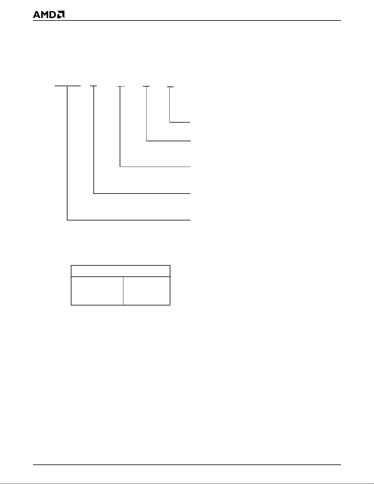
BLOCK DIAGRAM
CLK
RST
AD[31:00]
C/BE[3:0]
PAR
FRAME
TRDY
IRDY
STOP
IDSEL
DEVSEL
REQ
GNT
PERR
SERR
INTA
SLEEP
PCI Bus
Interface
Unit
Buffer
Management
Unit
Expansion Bus Interface
Bus
Rcv
FIFO
Bus
Xmt
FIFO
FIFO
Control
MAC
Rcv
FIFO
MAC
Xmt
FIFO
Network
Port
Manager
Auto
Negotiation
EBUA_EBA[7:0]
EBDA[15:8]
EBD[7:0]
EROMCS
ERAMCS
AS_EBOE
EBWE
EBCLK
802.3
MAC
Core
Manchester
Encoder/
Decoder
(PLS) &
AUI Port
10BASE-T
MAU
GPSI
Port
MII
Port
EADI
Port
TXEN
TXCLK
TXDAT
RXEN
RXCLK
RXDAT
CLSN
TX_E
TXD[3:0]
TX_EN
TX_CLK
COL
RXD[3:0]
RX_ER
RX_CLK
RX_DV
CRS
MDC
MDIO
SRDCLK
SRD
SF/BD
EAR
RXFRTGD/MIIRXFRTGD
RXFRTGE/MIIRXFRTGE
XTAL1
XTAL2
DO+/DI+/CI+/-
TXD+/TXP+/RXD+/-
TCK
TMS
TDI
TDO
JTAG
Port
Control
93C46
EEPROM
Interface
LED
Control
EECS
EESK
EEDI
EEDO
LED0
LED1
LED2
LED3
20550D-1
Am79C971 5
Page 6

TABLE OF CONTENTS
AM79C971 . . . . . . . . . . . . . . . . . . . . . . . . . . . . . . . . . . . . . . . . . . . . . . . . . . . . . . . . . . . . . . . . . . . . . . .1
DISTINCTIVE CHARACTERISTICS . . . . . . . . . . . . . . . . . . . . . . . . . . . . . . . . . . . . . . . . . . . . . . . . . . .1
GENERAL DESCRIPTION . . . . . . . . . . . . . . . . . . . . . . . . . . . . . . . . . . . . . . . . . . . . . . . . . . . . . . . . . .2
ORDERING INFORMATION . . . . . . . . . . . . . . . . . . . . . . . . . . . . . . . . . . . . . . . . . . . . . . . . . . . . . . . . .4
Standard Products . . . . . . . . . . . . . . . . . . . . . . . . . . . . . . . . . . . . . . . . . . . . . . . . . . . . . . . . . . . . . .4
BLOCK DIAGRAM. . . . . . . . . . . . . . . . . . . . . . . . . . . . . . . . . . . . . . . . . . . . . . . . . . . . . . . . . . . . . . . . .5
RELATED AMD PRODUCTS . . . . . . . . . . . . . . . . . . . . . . . . . . . . . . . . . . . . . . . . . . . . . . . . . . . . . . . 1 0
CONNECTION DIAGRAM (PQR160) . . . . . . . . . . . . . . . . . . . . . . . . . . . . . . . . . . . . . . . . . . . . . . . . .11
CONNECTION DIAGRAM (PQL176) . . . . . . . . . . . . . . . . . . . . . . . . . . . . . . . . . . . . . . . . . . . . . . . . .12
PIN DESIGNATIONS (PQR160) . . . . . . . . . . . . . . . . . . . . . . . . . . . . . . . . . . . . . . . . . . . . . . . . . . . . .13
Listed By Pin Number . . . . . . . . . . . . . . . . . . . . . . . . . . . . . . . . . . . . . . . . . . . . . . . . . . . . . . . . . .13
PIN DESIGNATIONS (PQL176). . . . . . . . . . . . . . . . . . . . . . . . . . . . . . . . . . . . . . . . . . . . . . . . . . . . . .14
Listed By Pin Number . . . . . . . . . . . . . . . . . . . . . . . . . . . . . . . . . . . . . . . . . . . . . . . . . . . . . . . . . .14
PIN DESIGNATIONS (PQR160, PQL176). . . . . . . . . . . . . . . . . . . . . . . . . . . . . . . . . . . . . . . . . . . . . .15
Listed By Group. . . . . . . . . . . . . . . . . . . . . . . . . . . . . . . . . . . . . . . . . . . . . . . . . . . . . . . . . . . . . . .15
PIN DESIGNATIONS. . . . . . . . . . . . . . . . . . . . . . . . . . . . . . . . . . . . . . . . . . . . . . . . . . . . . . . . . . . . . .16
Listed By Group. . . . . . . . . . . . . . . . . . . . . . . . . . . . . . . . . . . . . . . . . . . . . . . . . . . . . . . . . . . . . . .16
PIN DESIGNATIONS. . . . . . . . . . . . . . . . . . . . . . . . . . . . . . . . . . . . . . . . . . . . . . . . . . . . . . . . . . . . . .17
Listed By Group. . . . . . . . . . . . . . . . . . . . . . . . . . . . . . . . . . . . . . . . . . . . . . . . . . . . . . . . . . . . . . .17
Listed By Driver Type. . . . . . . . . . . . . . . . . . . . . . . . . . . . . . . . . . . . . . . . . . . . . . . . . . . . . . . . . . .17
PIN DESCRIPTIONS . . . . . . . . . . . . . . . . . . . . . . . . . . . . . . . . . . . . . . . . . . . . . . . . . . . . . . . . . . . . . .18
PCI Interface . . . . . . . . . . . . . . . . . . . . . . . . . . . . . . . . . . . . . . . . . . . . . . . . . . . . . . . . . . . . . . . . .18
AD[31:0]. . . . . . . . . . . . . . . . . . . . . . . . . . . . . . . . . . . . . . . . . . . . . . . . . . . . . . . . . . . . . . . . . . . . .18
C/BE[3:0] . . . . . . . . . . . . . . . . . . . . . . . . . . . . . . . . . . . . . . . . . . . . . . . . . . . . . . . . . . . . . . . . . . . .18
CLK . . . . . . . . . . . . . . . . . . . . . . . . . . . . . . . . . . . . . . . . . . . . . . . . . . . . . . . . . . . . . . . . . . . . . . . .18
DEVSEL. . . . . . . . . . . . . . . . . . . . . . . . . . . . . . . . . . . . . . . . . . . . . . . . . . . . . . . . . . . . . . . . . . . . .18
FRAME . . . . . . . . . . . . . . . . . . . . . . . . . . . . . . . . . . . . . . . . . . . . . . . . . . . . . . . . . . . . . . . . . . . . .18
GNT . . . . . . . . . . . . . . . . . . . . . . . . . . . . . . . . . . . . . . . . . . . . . . . . . . . . . . . . . . . . . . . . . . . . . . . .18
IDSEL . . . . . . . . . . . . . . . . . . . . . . . . . . . . . . . . . . . . . . . . . . . . . . . . . . . . . . . . . . . . . . . . . . . . . .18
INTA . . . . . . . . . . . . . . . . . . . . . . . . . . . . . . . . . . . . . . . . . . . . . . . . . . . . . . . . . . . . . . . . . . . . . . . .19
IRDY. . . . . . . . . . . . . . . . . . . . . . . . . . . . . . . . . . . . . . . . . . . . . . . . . . . . . . . . . . . . . . . . . . . . . . . .19
PAR . . . . . . . . . . . . . . . . . . . . . . . . . . . . . . . . . . . . . . . . . . . . . . . . . . . . . . . . . . . . . . . . . . . . . . . .19
PERR. . . . . . . . . . . . . . . . . . . . . . . . . . . . . . . . . . . . . . . . . . . . . . . . . . . . . . . . . . . . . . . . . . . . . . .20
Board Interface . . . . . . . . . . . . . . . . . . . . . . . . . . . . . . . . . . . . . . . . . . . . . . . . . . . . . . . . . . . . . . .20
LED0 . . . . . . . . . . . . . . . . . . . . . . . . . . . . . . . . . . . . . . . . . . . . . . . . . . . . . . . . . . . . . . . . . . . . . . .20
LED1 . . . . . . . . . . . . . . . . . . . . . . . . . . . . . . . . . . . . . . . . . . . . . . . . . . . . . . . . . . . . . . . . . . . . . . .20
LED2 . . . . . . . . . . . . . . . . . . . . . . . . . . . . . . . . . . . . . . . . . . . . . . . . . . . . . . . . . . . . . . . . . . . . . . .21
LED3 . . . . . . . . . . . . . . . . . . . . . . . . . . . . . . . . . . . . . . . . . . . . . . . . . . . . . . . . . . . . . . . . . . . . . . .21
SLEEP . . . . . . . . . . . . . . . . . . . . . . . . . . . . . . . . . . . . . . . . . . . . . . . . . . . . . . . . . . . . . . . . . . . . . .21
XTAL1 . . . . . . . . . . . . . . . . . . . . . . . . . . . . . . . . . . . . . . . . . . . . . . . . . . . . . . . . . . . . . . . . . . . . . .21
XTAL2 . . . . . . . . . . . . . . . . . . . . . . . . . . . . . . . . . . . . . . . . . . . . . . . . . . . . . . . . . . . . . . . . . . . . . .22
EEPROM Interface . . . . . . . . . . . . . . . . . . . . . . . . . . . . . . . . . . . . . . . . . . . . . . . . . . . . . . . . . . . .22
EECS. . . . . . . . . . . . . . . . . . . . . . . . . . . . . . . . . . . . . . . . . . . . . . . . . . . . . . . . . . . . . . . . . . . . . . .22
EEDI . . . . . . . . . . . . . . . . . . . . . . . . . . . . . . . . . . . . . . . . . . . . . . . . . . . . . . . . . . . . . . . . . . . . . . .22
EEDO. . . . . . . . . . . . . . . . . . . . . . . . . . . . . . . . . . . . . . . . . . . . . . . . . . . . . . . . . . . . . . . . . . . . . . .22
EESK . . . . . . . . . . . . . . . . . . . . . . . . . . . . . . . . . . . . . . . . . . . . . . . . . . . . . . . . . . . . . . . . . . . . . . .22
Expansion Bus Interface . . . . . . . . . . . . . . . . . . . . . . . . . . . . . . . . . . . . . . . . . . . . . . . . . . . . . . . .22
EBUA_EBA[7:0]. . . . . . . . . . . . . . . . . . . . . . . . . . . . . . . . . . . . . . . . . . . . . . . . . . . . . . . . . . . . . . .22
EBDA[15:8] . . . . . . . . . . . . . . . . . . . . . . . . . . . . . . . . . . . . . . . . . . . . . . . . . . . . . . . . . . . . . . . . . .23
EBD[7:0] . . . . . . . . . . . . . . . . . . . . . . . . . . . . . . . . . . . . . . . . . . . . . . . . . . . . . . . . . . . . . . . . . . . .23
EROMCS. . . . . . . . . . . . . . . . . . . . . . . . . . . . . . . . . . . . . . . . . . . . . . . . . . . . . . . . . . . . . . . . . . . .23
ERAMCS . . . . . . . . . . . . . . . . . . . . . . . . . . . . . . . . . . . . . . . . . . . . . . . . . . . . . . . . . . . . . . . . . . . .23
AS_EBOE . . . . . . . . . . . . . . . . . . . . . . . . . . . . . . . . . . . . . . . . . . . . . . . . . . . . . . . . . . . . . . . . . . .23
EBWE . . . . . . . . . . . . . . . . . . . . . . . . . . . . . . . . . . . . . . . . . . . . . . . . . . . . . . . . . . . . . . . . . . . . . .23
EBCLK. . . . . . . . . . . . . . . . . . . . . . . . . . . . . . . . . . . . . . . . . . . . . . . . . . . . . . . . . . . . . . . . . . . . . .23
Media Independent Interface . . . . . . . . . . . . . . . . . . . . . . . . . . . . . . . . . . . . . . . . . . . . . . . . . . . . .23
6 Am79C971
Page 7

TX_CLK . . . . . . . . . . . . . . . . . . . . . . . . . . . . . . . . . . . . . . . . . . . . . . . . . . . . . . . . . . . . . . . . . . . . .23
TXD[3:0]. . . . . . . . . . . . . . . . . . . . . . . . . . . . . . . . . . . . . . . . . . . . . . . . . . . . . . . . . . . . . . . . . . . . .23
TX_EN . . . . . . . . . . . . . . . . . . . . . . . . . . . . . . . . . . . . . . . . . . . . . . . . . . . . . . . . . . . . . . . . . . . . . .23
TX_ER . . . . . . . . . . . . . . . . . . . . . . . . . . . . . . . . . . . . . . . . . . . . . . . . . . . . . . . . . . . . . . . . . . . . . .24
COL . . . . . . . . . . . . . . . . . . . . . . . . . . . . . . . . . . . . . . . . . . . . . . . . . . . . . . . . . . . . . . . . . . . . . . . .24
CRS . . . . . . . . . . . . . . . . . . . . . . . . . . . . . . . . . . . . . . . . . . . . . . . . . . . . . . . . . . . . . . . . . . . . . . . .24
RX_CLK. . . . . . . . . . . . . . . . . . . . . . . . . . . . . . . . . . . . . . . . . . . . . . . . . . . . . . . . . . . . . . . . . . . . .24
RXD[3:0] . . . . . . . . . . . . . . . . . . . . . . . . . . . . . . . . . . . . . . . . . . . . . . . . . . . . . . . . . . . . . . . . . . . .24
RX_DV. . . . . . . . . . . . . . . . . . . . . . . . . . . . . . . . . . . . . . . . . . . . . . . . . . . . . . . . . . . . . . . . . . . . . .24
RX_ER. . . . . . . . . . . . . . . . . . . . . . . . . . . . . . . . . . . . . . . . . . . . . . . . . . . . . . . . . . . . . . . . . . . . . .25
MDC. . . . . . . . . . . . . . . . . . . . . . . . . . . . . . . . . . . . . . . . . . . . . . . . . . . . . . . . . . . . . . . . . . . . . . . .25
MDIO . . . . . . . . . . . . . . . . . . . . . . . . . . . . . . . . . . . . . . . . . . . . . . . . . . . . . . . . . . . . . . . . . . . . . . .25
Attachment Unit Interface . . . . . . . . . . . . . . . . . . . . . . . . . . . . . . . . . . . . . . . . . . . . . . . . . . . . . . .25
±. . . . . . . . . . . . . . . . . . . . . . . . . . . . . . . . . . . . . . . . . . . . . . . . . . . . . . . . . . . . . . . . . . . . . . . . . . . . . . . . . 25
CI
DI±. . . . . . . . . . . . . . . . . . . . . . . . . . . . . . . . . . . . . . . . . . . . . . . . . . . . . . . . . . . . . . . . . . . . . . . . . . . . . . . . . 25
DO±. . . . . . . . . . . . . . . . . . . . . . . . . . . . . . . . . . . . . . . . . . . . . . . . . . . . . . . . . . . . . . . . . . . . . . . . . . . . . . . . 25
10BASE-T Interface. . . . . . . . . . . . . . . . . . . . . . . . . . . . . . . . . . . . . . . . . . . . . . . . . . . . . . . . . . . .25
± . . . . . . . . . . . . . . . . . . . . . . . . . . . . . . . . . . . . . . . . . . . . . . . . . . . . . . . . . . . . . . . . . . . . . . . . . . . . . . 25
RXD
TXD±. . . . . . . . . . . . . . . . . . . . . . . . . . . . . . . . . . . . . . . . . . . . . . . . . . . . . . . . . . . . . . . . . . . . . . . . . . . . . . . 25
TXP±. . . . . . . . . . . . . . . . . . . . . . . . . . . . . . . . . . . . . . . . . . . . . . . . . . . . . . . . . . . . . . . . . . . . . . . . . . . . . . . 25
General Purpose Serial Interface . . . . . . . . . . . . . . . . . . . . . . . . . . . . . . . . . . . . . . . . . . . . . . . . . 2 5
CLSN . . . . . . . . . . . . . . . . . . . . . . . . . . . . . . . . . . . . . . . . . . . . . . . . . . . . . . . . . . . . . . . . . . . . . . .25
RXCLK. . . . . . . . . . . . . . . . . . . . . . . . . . . . . . . . . . . . . . . . . . . . . . . . . . . . . . . . . . . . . . . . . . . . . .26
RXDAT . . . . . . . . . . . . . . . . . . . . . . . . . . . . . . . . . . . . . . . . . . . . . . . . . . . . . . . . . . . . . . . . . . . . . .26
RXEN. . . . . . . . . . . . . . . . . . . . . . . . . . . . . . . . . . . . . . . . . . . . . . . . . . . . . . . . . . . . . . . . . . . . . . .26
TXCLK . . . . . . . . . . . . . . . . . . . . . . . . . . . . . . . . . . . . . . . . . . . . . . . . . . . . . . . . . . . . . . . . . . . . . .26
TXDAT . . . . . . . . . . . . . . . . . . . . . . . . . . . . . . . . . . . . . . . . . . . . . . . . . . . . . . . . . . . . . . . . . . . . . .26
TXEN . . . . . . . . . . . . . . . . . . . . . . . . . . . . . . . . . . . . . . . . . . . . . . . . . . . . . . . . . . . . . . . . . . . . . . .26
External Address Detection Interface . . . . . . . . . . . . . . . . . . . . . . . . . . . . . . . . . . . . . . . . . . . . . .26
EAR . . . . . . . . . . . . . . . . . . . . . . . . . . . . . . . . . . . . . . . . . . . . . . . . . . . . . . . . . . . . . . . . . . . . . . . .26
SFBD . . . . . . . . . . . . . . . . . . . . . . . . . . . . . . . . . . . . . . . . . . . . . . . . . . . . . . . . . . . . . . . . . . . . . . .26
SRD . . . . . . . . . . . . . . . . . . . . . . . . . . . . . . . . . . . . . . . . . . . . . . . . . . . . . . . . . . . . . . . . . . . . . . . .27
SRDCLK . . . . . . . . . . . . . . . . . . . . . . . . . . . . . . . . . . . . . . . . . . . . . . . . . . . . . . . . . . . . . . . . . . . .27
RXFRTGD . . . . . . . . . . . . . . . . . . . . . . . . . . . . . . . . . . . . . . . . . . . . . . . . . . . . . . . . . . . . . . . . . . .27
RXFRTGE . . . . . . . . . . . . . . . . . . . . . . . . . . . . . . . . . . . . . . . . . . . . . . . . . . . . . . . . . . . . . . . . . . .27
MIIRXFRTGD. . . . . . . . . . . . . . . . . . . . . . . . . . . . . . . . . . . . . . . . . . . . . . . . . . . . . . . . . . . . . . . . .27
MIIRXFRTGE. . . . . . . . . . . . . . . . . . . . . . . . . . . . . . . . . . . . . . . . . . . . . . . . . . . . . . . . . . . . . . . . .27
IEEE 1149.1 (1990) Test Access Port Interface. . . . . . . . . . . . . . . . . . . . . . . . . . . . . . . . . . . . . . .28
TCK . . . . . . . . . . . . . . . . . . . . . . . . . . . . . . . . . . . . . . . . . . . . . . . . . . . . . . . . . . . . . . . . . . . . . . . .28
TDI. . . . . . . . . . . . . . . . . . . . . . . . . . . . . . . . . . . . . . . . . . . . . . . . . . . . . . . . . . . . . . . . . . . . . . . . .28
TDO . . . . . . . . . . . . . . . . . . . . . . . . . . . . . . . . . . . . . . . . . . . . . . . . . . . . . . . . . . . . . . . . . . . . . . . .28
TMS . . . . . . . . . . . . . . . . . . . . . . . . . . . . . . . . . . . . . . . . . . . . . . . . . . . . . . . . . . . . . . . . . . . . . . . .28
Power Supply Pins. . . . . . . . . . . . . . . . . . . . . . . . . . . . . . . . . . . . . . . . . . . . . . . . . . . . . . . . . . . . .28
AV DDB. . . . . . . . . . . . . . . . . . . . . . . . . . . . . . . . . . . . . . . . . . . . . . . . . . . . . . . . . . . . . . . . . . . . . .28
AV SSB. . . . . . . . . . . . . . . . . . . . . . . . . . . . . . . . . . . . . . . . . . . . . . . . . . . . . . . . . . . . . . . . . . . . . .28
VDD_PLL. . . . . . . . . . . . . . . . . . . . . . . . . . . . . . . . . . . . . . . . . . . . . . . . . . . . . . . . . . . . . . . . . . . .28
VSS_PLL . . . . . . . . . . . . . . . . . . . . . . . . . . . . . . . . . . . . . . . . . . . . . . . . . . . . . . . . . . . . . . . . . . . .28
VDDB. . . . . . . . . . . . . . . . . . . . . . . . . . . . . . . . . . . . . . . . . . . . . . . . . . . . . . . . . . . . . . . . . . . . . . .28
VSSB . . . . . . . . . . . . . . . . . . . . . . . . . . . . . . . . . . . . . . . . . . . . . . . . . . . . . . . . . . . . . . . . . . . . . . .28
VDD_PCI . . . . . . . . . . . . . . . . . . . . . . . . . . . . . . . . . . . . . . . . . . . . . . . . . . . . . . . . . . . . . . . . . . . .28
VDD . . . . . . . . . . . . . . . . . . . . . . . . . . . . . . . . . . . . . . . . . . . . . . . . . . . . . . . . . . . . . . . . . . . . . . . .28
VSS . . . . . . . . . . . . . . . . . . . . . . . . . . . . . . . . . . . . . . . . . . . . . . . . . . . . . . . . . . . . . . . . . . . . . . . .28
BASIC FUNCTIONS . . . . . . . . . . . . . . . . . . . . . . . . . . . . . . . . . . . . . . . . . . . . . . . . . . . . . . . . . . . . . .29
System Bus Interface. . . . . . . . . . . . . . . . . . . . . . . . . . . . . . . . . . . . . . . . . . . . . . . . . . . . . . . . . . .29
Software Interface . . . . . . . . . . . . . . . . . . . . . . . . . . . . . . . . . . . . . . . . . . . . . . . . . . . . . . . . . . . . .29
Network Interfaces. . . . . . . . . . . . . . . . . . . . . . . . . . . . . . . . . . . . . . . . . . . . . . . . . . . . . . . . . . . . .29
DETAILED FUNCTIONS . . . . . . . . . . . . . . . . . . . . . . . . . . . . . . . . . . . . . . . . . . . . . . . . . . . . . . . . . . .30
Slave Bus Interface Unit. . . . . . . . . . . . . . . . . . . . . . . . . . . . . . . . . . . . . . . . . . . . . . . . . . . . . . . . .30
Am79C971 7
Page 8

Slave Configuration Transfers . . . . . . . . . . . . . . . . . . . . . . . . . . . . . . . . . . . . . . . . . . . . . . . . . . . .30
Slave I/O Transfers. . . . . . . . . . . . . . . . . . . . . . . . . . . . . . . . . . . . . . . . . . . . . . . . . . . . . . . . . . . . .30
Master Bus Interface Unit . . . . . . . . . . . . . . . . . . . . . . . . . . . . . . . . . . . . . . . . . . . . . . . . . . . . . . .36
Buffer Management Unit . . . . . . . . . . . . . . . . . . . . . . . . . . . . . . . . . . . . . . . . . . . . . . . . . . . . . . . .53
Software Interrupt Timer . . . . . . . . . . . . . . . . . . . . . . . . . . . . . . . . . . . . . . . . . . . . . . . . . . . . . . . .59
Media Access Control . . . . . . . . . . . . . . . . . . . . . . . . . . . . . . . . . . . . . . . . . . . . . . . . . . . . . . . . . .60
Transmit Operation. . . . . . . . . . . . . . . . . . . . . . . . . . . . . . . . . . . . . . . . . . . . . . . . . . . . . . . . . . . . .63
Receive Operation. . . . . . . . . . . . . . . . . . . . . . . . . . . . . . . . . . . . . . . . . . . . . . . . . . . . . . . . . . . . .66
Loopback Operation. . . . . . . . . . . . . . . . . . . . . . . . . . . . . . . . . . . . . . . . . . . . . . . . . . . . . . . . . . . .68
Manchester Encoder/Decoder. . . . . . . . . . . . . . . . . . . . . . . . . . . . . . . . . . . . . . . . . . . . . . . . . . . .70
Attachment Unit Interface . . . . . . . . . . . . . . . . . . . . . . . . . . . . . . . . . . . . . . . . . . . . . . . . . . . . . . .72
Twisted-Pair Transceiver . . . . . . . . . . . . . . . . . . . . . . . . . . . . . . . . . . . . . . . . . . . . . . . . . . . . . . . .72
General Purpose Serial Interface . . . . . . . . . . . . . . . . . . . . . . . . . . . . . . . . . . . . . . . . . . . . . . . . . 7 5
Full-Duplex Operation . . . . . . . . . . . . . . . . . . . . . . . . . . . . . . . . . . . . . . . . . . . . . . . . . . . . . . . . . .75
Media Independent Interface . . . . . . . . . . . . . . . . . . . . . . . . . . . . . . . . . . . . . . . . . . . . . . . . . . . . .76
Auto-Negotiation . . . . . . . . . . . . . . . . . . . . . . . . . . . . . . . . . . . . . . . . . . . . . . . . . . . . . . . . . . . . . .79
Automatic Network Port Selection . . . . . . . . . . . . . . . . . . . . . . . . . . . . . . . . . . . . . . . . . . . . . . . . .79
External Address Detection Interface (EADI). . . . . . . . . . . . . . . . . . . . . . . . . . . . . . . . . . . . . . . . .81
Expansion Bus Interface . . . . . . . . . . . . . . . . . . . . . . . . . . . . . . . . . . . . . . . . . . . . . . . . . . . . . . . .84
EEPROM Interface . . . . . . . . . . . . . . . . . . . . . . . . . . . . . . . . . . . . . . . . . . . . . . . . . . . . . . . . . . . .94
LED Support . . . . . . . . . . . . . . . . . . . . . . . . . . . . . . . . . . . . . . . . . . . . . . . . . . . . . . . . . . . . . . . . .97
Power Savings Modes . . . . . . . . . . . . . . . . . . . . . . . . . . . . . . . . . . . . . . . . . . . . . . . . . . . . . . . . . .97
IEEE 1149.1 (1990) Test Access Port Interface. . . . . . . . . . . . . . . . . . . . . . . . . . . . . . . . . . . . . . .99
The contents of the Device ID register is the same as the contents of CSR88. . . . . . . . . . . . . .100
NAND Tree Testing . . . . . . . . . . . . . . . . . . . . . . . . . . . . . . . . . . . . . . . . . . . . . . . . . . . . . . . . . . .100
Reset . . . . . . . . . . . . . . . . . . . . . . . . . . . . . . . . . . . . . . . . . . . . . . . . . . . . . . . . . . . . . . . . . . . . . .102
Software Access . . . . . . . . . . . . . . . . . . . . . . . . . . . . . . . . . . . . . . . . . . . . . . . . . . . . . . . . . . . . .102
USER ACCESSIBLE REGISTERS . . . . . . . . . . . . . . . . . . . . . . . . . . . . . . . . . . . . . . . . . . . . . . . . . .106
PCI Configuration Registers . . . . . . . . . . . . . . . . . . . . . . . . . . . . . . . . . . . . . . . . . . . . . . . . . . . .108
RAP Register. . . . . . . . . . . . . . . . . . . . . . . . . . . . . . . . . . . . . . . . . . . . . . . . . . . . . . . . . . . . . . . .114
Control and Status Registers. . . . . . . . . . . . . . . . . . . . . . . . . . . . . . . . . . . . . . . . . . . . . . . . . . . .115
Bus Configuration Registers . . . . . . . . . . . . . . . . . . . . . . . . . . . . . . . . . . . . . . . . . . . . . . . . . . . .148
Initialization Block . . . . . . . . . . . . . . . . . . . . . . . . . . . . . . . . . . . . . . . . . . . . . . . . . . . . . . . . . . . .180
Receive Descriptors. . . . . . . . . . . . . . . . . . . . . . . . . . . . . . . . . . . . . . . . . . . . . . . . . . . . . . . . . . .183
Transmit Descriptors . . . . . . . . . . . . . . . . . . . . . . . . . . . . . . . . . . . . . . . . . . . . . . . . . . . . . . . . . .186
REGISTER SUMMARY . . . . . . . . . . . . . . . . . . . . . . . . . . . . . . . . . . . . . . . . . . . . . . . . . . . . . . . . . . .190
PCI Configuration Registers . . . . . . . . . . . . . . . . . . . . . . . . . . . . . . . . . . . . . . . . . . . . . . . . . . . .190
Control and Status Registers. . . . . . . . . . . . . . . . . . . . . . . . . . . . . . . . . . . . . . . . . . . . . . . . . . . .191
Bus Configuration Registers . . . . . . . . . . . . . . . . . . . . . . . . . . . . . . . . . . . . . . . . . . . . . . . . . . . .195
REGISTER PROGRAMMING SUMMARY . . . . . . . . . . . . . . . . . . . . . . . . . . . . . . . . . . . . . . . . . . . .196
Am79C971 Programmable Registers . . . . . . . . . . . . . . . . . . . . . . . . . . . . . . . . . . . . . . . . . . . . .196
ABSOLUTE MAXIMUM RATINGS . . . . . . . . . . . . . . . . . . . . . . . . . . . . . . . . . . . . . . . . . . . . . . . . . .200
OPERATING RANGES . . . . . . . . . . . . . . . . . . . . . . . . . . . . . . . . . . . . . . . . . . . . . . . . . . . . . . . . . . .200
DC CHARACTERISTICS OV ER COMMERCIAL OPERATING RANGES UNLESS OTHERWISE
SPECIFIED . . . . . . . . . . . . . . . . . . . . . . . . . . . . . . . . . . . . . . . . . . . . . . . . . . . . . . . . . . . . . . . . . . . .200
SWITCHING CHARACTERISTICS: BUS INTERFACE. . . . . . . . . . . . . . . . . . . . . . . . . . . . . . . . . . .203
SWITCHING CHARACTERISTICS: 10BASE-T INTERFACE. . . . . . . . . . . . . . . . . . . . . . . . . . . . . .206
SWITCHING CHARACTERISTICS: ATTACHMENT UNIT INTERFACE. . . . . . . . . . . . . . . . . . . . . .207
SWITCHING CHARACTERISTICS: MEDIA INDEPENDENT INTERFACE . . . . . . . . . . . . . . . . . . .208
SWITCHING CHARACTERISTICS: GENERAL-PURPOSE SERIAL INTERFACE . . . . . . . . . . . . .209
SWITCHING CHARACTERISTICS: EXTERNAL ADDRESS DETECTION INTERFACE . . . . . . . .210
KEY TO SWITCHING WAVEFORMS . . . . . . . . . . . . . . . . . . . . . . . . . . . . . . . . . . . . . . . . . . . . . . . .211
SWITCHING TEST CIRCUITS. . . . . . . . . . . . . . . . . . . . . . . . . . . . . . . . . . . . . . . . . . . . . . . . . . . . . .211
SWITCHING WAVEFORMS: SYSTEM BUS INTERFACE . . . . . . . . . . . . . . . . . . . . . . . . . . . . . . . .213
SWITCHING WAVEFORMS: EXPANSION BUS INTERFACE. . . . . . . . . . . . . . . . . . . . . . . . . . . . .217
SWITCHING WAVEFORMS: 10BASE-T INTERFACE . . . . . . . . . . . . . . . . . . . . . . . . . . . . . . . . . . .219
SWITCHING WAVEFORMS: ATTACHMENT UNIT INTERFACE . . . . . . . . . . . . . . . . . . . . . . . . . .221
SWITCHING WAVEFORMS: MEDIA INDEPENDENT INTERFACE . . . . . . . . . . . . . . . . . . . . . . . .224
8 Am79C971
Page 9

SWITCHING WAVEFORMS: GENERAL-PURPOSE SERIAL INTERFACE . . . . . . . . . . . . . . . . . .226
SWITCHING WAVEFORMS: EXTERNAL ADDRESS DETECTION INTERFACE. . . . . . . . . . . . . .227
SWITCHING WAVEFORMS: RECEIVE FRAME TAG. . . . . . . . . . . . . . . . . . . . . . . . . . . . . . . . . . . .228
PHYSICAL DIMENSIONS* . . . . . . . . . . . . . . . . . . . . . . . . . . . . . . . . . . . . . . . . . . . . . . . . . . . . . . . .229
PQR160. . . . . . . . . . . . . . . . . . . . . . . . . . . . . . . . . . . . . . . . . . . . . . . . . . . . . . . . . . . . . . . . . . . .229
PQL176 . . . . . . . . . . . . . . . . . . . . . . . . . . . . . . . . . . . . . . . . . . . . . . . . . . . . . . . . . . . . . . . . . . . .230
AM79C971 COMPATIBLE MEDIA INTERFACE MODULES. . . . . . . . . . . . . . . . . . . . . . . . . . . . . .A-1
RECOMMENDATION FOR POWER AND GROUND DECOUPLING. . . . . . . . . . . . . . . . . . . . . . . .B-1
ALTERNATIVE METHOD FOR INITIALIZATION* . . . . . . . . . . . . . . . . . . . . . . . . . . . . . . . . . . . . . .C-1
LOOK-AHEAD PACKET PROCESSING (LAPP) CONCEPT. . . . . . . . . . . . . . . . . . . . . . . . . . . . . .D-1
AUTO-NEGOTIATION REGISTERS . . . . . . . . . . . . . . . . . . . . . . . . . . . . . . . . . . . . . . . . . . . . . . . . .E-1
AM79C971A PCNET-FAST 10/100 MBPS PCI ETHERNET CONTROLLER REV A.6 ERRATA . . F-1
Am79C971 9
Page 10

RELATED AMD PRODUCTS
Part No. Description
Am79C90 CMOS Local Area Network Controller for Ethernet (C-LANCE)
Am7996 IEEE 802.3/Ethernet/Cheapernet Tap Transceiver
Am79C98 Twisted Pair Ethernet Transceiver (TPEX)
Am79C100 Twisted Pair Ethernet Transceiver Plus (TPEX+)
Am79865 100 Mbps Physical Data Transmitter (PDT)
An79866A 100 Mbps Physical Data Receiver (PDR)
Am79C870 Quad 100BASE-X Transceiver
Am79C871 Quad 100BASE-X Repeater Transceiver
Am79C940 Media Access Controller for Ethernet (MACE™)
Am79C960 PCnet-ISA Single-Chip Ethernet Controller (for ISA bus)
Am79C961 PCnet-ISA+ Single-Chip Ethernet Controller (with Microsoft® Plug n' Play support)
Am79C961A PCnet-ISA II Single-Chip Full-Duplex Ethernet Controller (with Microsoft® Plug n' Play support)
Am79C965 PCnet-32 Single-Chip 32-Bit Ethernet Controller (for 486 and VL buses)
Am79C970A PCnet-PCI II Single-Chip Full-Duplex Ethernet Controller for PCI Local Bus
Am79C981 Integrated Multiport R epeater Plus™ (IMR+™)
Am79C987 Hardware Implemented Management Information Base™ (HIMIB™)
10 Am79C971
Page 11

CONNECTION DIAGRAM (PQR160)
D
IDSEL
VDD
AD23
AD22
VSS
AD21
AD20
VDD_PCI
AD19
AD18
VSSB
AD17
AD16
C/BE2
FRAME
IRDY
TRDY
DEVSEL
STOP
VSSB
PERR
SERR
VDD_PCI
PAR
C/BE1
AD15
AD14
AD13
AD12
VSSB
AD11
AD10
VDD
AD9
AD8
VSS
C/BE0
AD7
AD6
VSSB
AD27
AD26
VDD_PCI
AD25
AD24
C/BE3
VSSB
160
159
158
1
2
3
4
5
6
7
8
9
10
11
12
13
14
15
16
17
18
19
20
21
22
23
24
25
26
27
28
29
30
31
32
33
34
35
36
37
38
39
40
157
414243444546474849505152535455565758596061626364656667687071727374757677787980
156
155
154
AD29
AD28
153
152
AD30
VDD
151
150
AD31
CLK
VSSB
REQ
GNT
149
148
147
146
145
PCnet™-
Am79C971 KC/W
Am79C971
VSS
144
RST
143
INTA
142
TDI
VDD_PCI
141
140
FAST
TDO
TMS
139
138
TCK
137
VSSB
EECS
136
135
VDDB
VDD_PLL
LED2/SRDCLK/MIIRXFRTGE
EESK/LED1/SFBD
EEDI/LED0
EEDO/LED3/SRD/MIIRXFRTG
CI+
CI-
DI+
134
133
131
130
129
128
127
132
69
126
AVDDB
DI-
125
124
DO+
DO-
123
122
AVSSB
121
120
119
118
117
116
115
114
113
112
111
110
109
108
107
106
105
104
103
102
101
100
99
98
97
96
95
94
93
92
91
90
89
88
87
86
85
84
83
82
81
XTAL2
VSS_PLL
XTAL1
AVDDB
TXD+
TXP+
TXDTXPAVDDB
RXD+
RXDVSS
MDIO
MDC
SLEEP/EAR
RXD3
RXD2
RXD1
RXD0/RXFRTGD
VDDB
RX_DV/RXFRTGE
RX_CLK/RXCLK
RX_ER/RXDAT
VSSB
TX_ER
TX_CLK/TXCLK
TX_EN/TXEN
VDDB
TXD0/TXDAT
TXD1
TXD2
TXD3
COL/CLSN
CRS/RXEN
VSSB
EBD0
EBD1
EBD2
EBD3
EBD4
AD5
AD4
AD3
Pin 1 is marked for orientation.
AD1
AD2
VDD_PCI
AD0
VSSB
EBWE
ERAMCS
AS_EBOE
EBROMCS
2055A-2
VSS
EBCLK
EBUA_EBA0
EBUA_EBA1
VSSB
VDDB
EBUA_EBA2
EBUA_EBA3
EBUA_EBA4
VDDB
EBDA8
EBUA_EBA5
EBUA_EBA6
EBUA_EBA7
EBDA9
EBDA10
EBDA11
VSSB
EBDA12
VDD
EBDA13
EBDA14
EBDA15
EBD6
EBD7
EBD5
VSSB
VSS
Am79C971 11
20550D-2
Page 12

CONNECTION DIAGRAM (PQL176)
NCNCAD24
C/BE3
VSSB
AD25
VDD_PCI
AD26
AD27
AD28
AD29
AD30
VDD
AD31
176
175
174
173
172
171
170
169
168
167
166
165
164
NC
NC
IDSEL
VDD
AD23
AD22
VSS
AD21
AD20
VDD_PCI
AD19
AD18
VSSB
AD17
AD16
C/BE2
FRAME
IRDY
TRDY
DEVSEL
STOP
VSSB
PERR
SERR
VDD_PCI
PAR
C/BE1
AD15
AD14
AD13
AD12
VSSB
AD11
AD10
VDD
AD9
AD8
VSS
C/BE0
AD7
AD6
VSSB
NC
NC
1
2
3
4
5
6
7
8
9
10
11
12
13
14
15
16
17
18
19
20
21
22
23
24
25
26
27
28
29
30
31
32
33
34
35
36
37
38
39
40
41
42
43
44
45464748495051525354555657585960616263646566676869707172737475767778798081828384858687
163
REQ
GNT
VSSB
CLK
VSS
RST
162
161
160
159
158
157
PCnetª-
Am79C971 VC/W
Am79C971
INTA
VDD_PCI
156
155
TDI
154
TDO
TMS
153
152
FAST
VC/W
TCK
EECS
VSSB
EESK/LED1/SFBD
LED2/SRDCLK/MIIRXFRTGE
EEDI/LED0
151
150
149
148
147
146
EEDO/LED3/SRD/MIIRXFRTGD
VDDB
VDD_PLL
CI+
CI-
DI+
DI-
AVDDB
DO+
DO-
AVSSBNCNC
145
144
143
142
141
140
139
138
137
136
135
134
133
132
131
130
129
128
127
126
125
124
123
122
121
120
119
118
117
116
115
114
113
112
111
110
109
108
107
106
105
104
103
102
101
100
NC
NC
XTAL2
VSS_PLL
XTAL1
AVDDB
TXD+
TXP+
TXDTXPAVDDB
RXD+
RXDVSS
MDIO
MDC
SLEEP/EAR
RXD3
RXD2
RXD1
RXD0/RXFRTGD
VDDB
RX_DV/RXFRTGE
RX_CLK/RXCLK
RX_ER/RXDAT
VSSB
TX_ER
TX_CLTXCLK
TX_EN/TXEN
VDDB
TXD0/TXDAT
TXD1
TXD2/RXEN
TXD3
99
COL/CLSN
98
CRS/RXEN
97
VSSB
96
EBD0
95
EBD1
94
EBD2
93
EBD3
92
EBD4
91
NC
90
NC
89
88
NC
NC
AD5
AD4
AD3
AD2
AD1
AD0
VDD_PCI
VSSB
ERAMCS
EBWE
AS_EBOE
EBROMCS
VSS
EBCLK
EBUA_EBA0
EBUA_EBA1
EBUA_EBA2
EBUA_EBA3
VSSB
VDDB
EBUA_EBA4
EBUA_EBA5
EBUA_EBA6
EBUA_EBA7
Pin 1 is marked for orientation.
12 Am79C971
VDDB
EBDA8
EBDA9
EBDA10
VSSB
EBDA11
EBDA12
EBDA13
VDD
EBDA14
EBDA15
EBD7
EBD6
VSSB
EBD5
VSS
NC
NC
20550D-3
Page 13

PIN DESIGNATIONS (PQR16 0)
Listed By Pin Number
Pin
Pin
No.
Name
1 IDSEL 41 AD5 81 EBD4 121 AVSSB
2 VDD 42 AD4 82 EBD3 122 DO3 AD23 43 AD3 83 EBD2 123 DO+
4 AD22 44 AD2 84 EBD1 124 AVDDB
5 VSS 45 VDD_PCI 85 EBD0 125 DI6 AD21 46 AD1 86 VSSB 126 DI+
7 AD20 47 AD0 87 CRS/RXEN 127 CI8 VDD_PCI 48 VSSB 88 COL/CLSN 128 CI+
9 AD19 49 ERAMCS 89 TXD3 129 VDD_PLL
10 AD18 50 EROMCS 90 TXD2 130 VDDB
11 VSSB 51 EBWE 91 TXD1 131
12 AD17 52 AS_EBOE 92 TXD0/TXDAT 132 EED1/LED0
13 AD16 53 EBCLK 93 VDDB 133
14 C/BE2 54 VSS 94 TX_EN/TXEN 134 EESK/LED1/SFBD
15 FRAME 55 EBUA_EBA0 95 TX_CLK/TXCLK 135 VSSB
16 IRDY 56 EBUA_EBA1 96 TX_ER 136 EECS
17 TRDY 57 EBUA_EBA2 97 VSSB 137 TCK
18 DEVSEL 58 EBUA_EBA3 98 RX_ER/RXDAT 138 TMS
19 STOP 59 VSSB 99 RX_CLK/RXCLK 139 TDO
20 VSSB 60 EBUA_EBA4 100 RX_DV/RXFRTGE 140 TDI
21 PERR 61 VDDB 101 VDDB 141 VDD_PCI
22 SERR 62 EBUA_EBA5 102 RXD0/RXFRTGD 142 INTA
23 VDD_PCI 63 EBUA_EBA6 103 RXD1 143 RST
24 PAR 64 EBUA_EBA7 104 RXD2 144 VSS
25 C/BE1 65 VDDB 105 RXD3 145 CLK
26 AD15 66 EBDA8 106 SLEEP/EAR 146 VSSB
27 AD14 67 EBDA9 107 MDC 147 GNT
28 AD13 68 EBDA10 108 MDIO 148 REQ
29 AD12 69 EBDA11 109 VSS 149 AD31
30 VSSB 70 VSSB 110 RXD- 150 VDD
31 AD11 71 EBDA12 111 RXD+ 151 AD30
32 AD10 72 EBDA13 112 AVDDB 152 AD29
33 VDD 73 VDD 113 TXP- 153 AD28
34 AD9 74 EBDA14 114 TXD- 154 AD27
35 AD8 75 EBDA15 115 TXP+ 155 AD26
36 VSS 76 EBD7 116 TXD+ 156 VDD_PCI
37 C/BE0 77 EBD6 117 AVDDB 157 AD25
38 AD7 78 VSSB 118 XTAL1 158 VSSB
39 AD6 79 EBD5 119 VSS_PLL 159 C/BE3
40 VSSB 80 VSS 120 XTAL2 160 AD24
Pin
No.
Pin
Name
Pin
No.
Pin
Name
Pin No.
Pin
Name
EEDO/LED3/SRD/
MIIRXFRTGD
LED2/SRDCLK/
MIIRXFRTGE
Am79C971 13
Page 14

PIN DESIGNATIONS (PQL176)
Listed By Pin Number
Pin
Pin
No.
Name
1 NC 45 NC 89 NC 133 NC
2 NC 46 NC 90 NC 134 NC
3 IDSEL 47 AD5 91 EBD4 135 AVSSB
4 VDD 48 AD4 92 EBD3 136 DO5 AD23 49 AD3 93 EBD2 137 DO+
6 AD22 50 AD2 94 EBD1 138 AVDDB
7 VSS 51 VDD_PCI 95 EBD0 139 DI8 AD21 52 AD1 96 VSSB 140 DI+
9 AD20 53 AD0 97 CRS/RXEN 141 CI10 VDD_PCI 54 VSSB 98 COL/CLSN 142 CI+
11 AD19 55 ERAMCS 99 TXD3 143 VDD_PLL
12 AD18 56 EROMCS 100 TXD2/RXEN 144 VDDB
13 VSSB 57 EBWE 101 TXD1 145
14 AD17 58 AS_EBOE 102 TXD0/TXDAT 146 EED1/LED0
15 AD16 59 EBCLK 103 VDDB 147
16 C/BE2 60 VSS 104 TX_EN/TXEN 148 EESK/LED1/SFBD
17 FRAME 61 EBUA_EBA0 105 TX_CLK/TXCLK 149 VSSB
18 IRDY 62 EBUA_EBA1 106 TX_ER 150 EECS
19 TRDY 63 EBUA_EBA2 107 VSSB 151 TCK
20 DEVSEL 64 EBUA_EBA3 108 RX_ER/RXDAT 152 TMS
21 STOP 65 VSSB 109 RX_CLK/RXCLK 153 TDO
22 VSSB 66 EBUA_EBA4 110 RX_DV/RXFRTGE 154 TDI
23 PERR 67 VDDB 111 VDDB 155 VDD_PCI
24 SERR 68 EBUA_EBA5 112 RXD0/RXFRTGD 156 INTA
25 VDD_PCI 69 EBUA_EBA6 113 RXD1 157 RST
26 PAR 70 EBUA_EBA7 114 RXD2 158 VSS
27 C/BE1 71 VDDB 115 RXD3 159 CLK
28 AD15 72 EBDA8 116 SLEEP/EAR 160 VSSB
29 AD14 73 EBDA9 117 MDC 161 GNT
30 AD13 74 EBDA10 118 MDIO 162 REQ
31 AD12 75 EBDA11 119 VSS 163 AD31
32 VSSB 76 VSSB 120 RXD- 164 VDD
33 AD11 77 EBDA12 121 RXD+ 165 AD30
34 AD10 78 EBDA13 122 AVDDB 166 AD29
35 VDD 79 VDD 123 TXP- 167 AD28
36 AD9 80 EBDA14 124 TXD- 168 AD27
37 AD8 81 EBDA15 125 TXP+ 169 AD26
38 VSS 82 EBD7 126 TXD+ 170 VDD_PCI
39 C/BE0 83 EBD6 127 AVDDB 171 AD25
40 AD7 84 VSSB 128 XTAL1 172 VSSB
41 AD6 85 EBD5 129 VSS_PLL 173 C/BE3
42 VSSB 86 VSS 130 XTAL2 174 AD24
43 NC 87 NC 131 NC 175 NC
44 NC 88 NC 132 NC 176 NC
Pin
No.
Pin
Name
Pin
No.
Pin
Name
Pin No.
Pin
Name
EEDO/LED3/SRD/
MIIRXFRTGD
LED2/SRDCLK/
MIIRXFRTGE
14 Am79C971
Page 15

PIN DESIGNATIONS (PQR160, PQL176)
Listed By Group
Pin Name Pin Function Type
PCI Bus Interface
AD[31:0] Address/Data Bus IO TS3 32
C/BE[3:0] Bus Command/Byte Enable IO TS3 4
CLK Bus Clock I NA 1
DEVSEL Device Select IO STS6 1
FRAME Cycle Fram e IO STS6 1
GNT Bus Grant I NA 1
IDSEL Initialization Device Select I NA 1
INTA Interrupt O OD6 1
IRDY Initiator Ready IO STS6 1
PAR Parity IO TS3 1
PERR Parity Error IO STS6 1
REQ Bus Request O TS3 1
RST Reset I NA 1
SERR System Error IO OD6 1
STOP Stop IO STS6 1
TRDY Target Ready IO STS6 1
Board Interface
LED0 LED0 O LED 1
LED1 LED1 O LED 1
LED2 LED2 O LED 1
LED3 LED3 O LED 1
SLEEP Sleep Mode I NA 1
XTAL1 Crystal Input I NA 1
XTAL2 Crystal Output O XTAL 1
EEPROM Interface
EECS Serial EEPROM Chip Select O O6 1
EEDI Serial EEPROM Data In O LED 1
EEDO Serial EEPROM Data Out I NA 1
EESK Serial EEPROM Clock IO LED 1
Expansion ROM Interface
AS_EBOE Address Strobe/Expansion Bus Output Enable O O6 1
EBCLK Expansion Bus Clock I NA 1
EBD[7:0] Expansion Bus Data [7:0] IO TS6 8
EBDA[15:8] Expansion Bus Data/Address [15:8] IO TS6 8
EBUA_EBA[7:0]
EBWE Expansion Bus Write Enable O O6 1
ERAMCS Expansion Bus RAM Chip Select O O6 1
EROMCS Expansion Bus ROM Chip Select O O6 1
Note:
1. Not including test features
Expansion Bus Upper Addres s /Expansion Bus Addres s
[7:0]
1
O O6 8
Driver No. of Pins
Am79C971 15
Page 16

PIN DESIGNATIONS
Listed By Group
Pin Name Pin Function Type
Media Independent Interface (MII)
COL Collision I NA 1
CRS Carrier Sense I NA 1
MDC Management Data Clock O OMII2 1
MDIO Management Data I/O IO TSMII 1
RX_CLK Receive Clock I NA 1
RXD[3:0] Receive Data I NA 4
RX_DV Receive Data Valid I NA 1
RX_ER Receive Error I NA 1
TX_CLK Transmit Clock I NA 1
TXD[3:0] Transmit Data O OMII1 4
TX_EN Transmit Data Enable O OMII1 1
TX_ER Transmit Error O OMII1 1
Attachment Unit Interface (A UI)
CI± AUI Collis ion I NA 1
DI± AUI Data In I NA 1
DO± AUI Data Out O DO 1
10BASE-T Interface
RXD+/RXD- Receive Differential Pair I NA 2
TXD+/TXD- Transmit Differential Pair O TDO 2
TXP+/TXP- Transmit Pre-distortion Differential Pair O TPO 2
General Purpose Serial Interface (GPSI)
CLSN Collision IO NA 1
RXCLK Receive Clock I NA 1
RXDAT Receive Data I NA 1
RXEN Receive Enable I NA 1
TXCLK Transmit Clock I NA 1
TXDAT Transmit Data O O6 1
TXEN Transmit Enable O O6 1
External Address Detection Interface (EADI)
EAR External Address Reject Low I NA 1
SFBD Start Frame Byte Delimiter O LED 1
SRD Serial Receive Data IO LED 1
SRDCLK Serial Receive Data Clock IO LED 1
RXFRTGD/MIIRXFRTGD
RXFRTGE/MIIRXFRTGE
IEEE 1149.1 Test Access Port Interface (JTAG)
TCK Test Clock I NA 1
TDI Test Data In I NA 1
TDO Test Data Out O TS6 1
TMS Test Mode Sele ct I NA 1
Note:
1. Not including test features.
Receive Frame Tag Data/MII Receive Frame
Tag Data
Receive Frame T ag Enable/MII Receive Fr ame
Tag Enable
1
I NA 1
I NA 1
Driver No. of Pins
16 Am79C971
Page 17

PIN DESIGNATIONS
Listed By Group
Pin Name Pin Function Type
Power Suppli es
AVDDB Analog I/O Buffer Power P NA 3
AVSSB Analog I/O Buffer Ground P NA 1
VDD_PLL Analog PLL Power P NA 1
VSS_PLL Analog PLL Ground P NA 1
VDD Digital Power P NA 4
VSS Digital Ground P NA 6
VDDB I/O Buffer Power P NA 5
VSSB I/O Buffer Ground P NA 13
VDD_PCI PCI I/O Buffer Power P NA 5
Note:
1. Not including test features.
1
Driver No. of Pins
Listed By Driver Type
The following table describes th e various type s of o utput drive rs used i n the Am79C9 71 contro ller . All I
values shown in the table apply to 5 V signaling.
I
OH
See the DC Characteristics section for the values ap-
OL
and
A sustained tri-state signal is a low active signal that is
driven high for one clock period before it is left floating.
DO, TDO, and TPO are differential output drivers. Their
characteristics and t he o ne of the XTAL output a re described in the DC Characteristics section.
plying to 3.3 V signaling.
Name Type IOL (mA) IOH (mA) Load (pF)
LED LED 12 -0.4 50
OMII1 Totem Pole 4 -4 50
OMII2 Totem Pole 4 -4 390
O6 Totem Pole 6 -0.4 50
OD6 Open Drain 6 NA 50
STS6 Sustained Tri-State 6 -2 50
TS3 Tri-State 3 -2 50
TS6 Tri-State 6 -2 50
TSMII Tri-State 4 -4 470
Am79C971 17
Page 18

PIN DESCRIPTIONS
PCI Interfa ce
AD[31:0]
Address and Data Input/Output
Address and data ar e multi pl exed on the same bus in terface pins. During the fir st clock of a transaction,
AD[31:0] contain a physical address (32 bits). During
the subsequent clocks, AD[31:0] contain data. Byte ordering is littl e endian by default. AD[07:0] are define d
as the least significant byte (LSB) and AD[31:24] are
defined as the most significant byte (MSB). For FIFO
data transfers, the Am79C971 controller can be programmed for big endian byte ordering. See CSR3, bit 2
(BSWP) for more details.
eration section for details. The Am79C971 controller
will support a clock frequency of 0 MHz after certain
precautions are taken to ensure data integrity. This
clock or a derivation i s not used to dr ive any network
functions.
When RST
testing.
is active, CLK is an inp ut for NAND tree
DEVSEL
Device Select Input/Output
The Am79C971 controller dr ives DEVSEL when it detects a transaction that selects the device as a target.
The device samples DEVSEL
claims a transaction that the Am79C971 controller has
initiated.
to detect if a target
During the address phase of the transaction, when the
Am79C971 controller is a bus master , AD[31:2] will address the active Double Word (DWord). The
Am79C971 controller alwa ys drives AD[1:0] to ’00’ dur-
ing the address phase indicating linear burst order.
When the Am79C971 controller is not a bus master, the
AD[31:0] lines are continuously monitored to determine
if an address match exists for slave transfers.
During the data phase of the transacti on, AD[31: 0] are
driven by the Am79C971 controller wh en performing
bus master write and slave read operations. Data on
AD[31:0] is latched by the Am79C971 co ntroller when
performing bus master read and slave write operations.
When RST
testing.
is active, AD[31:0] are inputs for NAND tree
C/BE[3:0]
Bus Command and Byte Enables Input/Output
Bus command and byte enables are multiplexed on the
same bus interface pins. During the a ddress phase o f
the transaction, C /BE
During the data phase, C/BE
ables. The byte enables define which physical byte
lanes carry meaningful data. C/BE
(AD[07:0]) and C/BE
The function of the byte enables is ind ependen t of th e
byte ordering mode (BSWP, CSR3, bit 2).
When RST
tree testing.
is active, C/BE[3:0] are inputs for NAND
[3:0] define th e bus command.
[3:0] are used as byte en -
0 applies to byte 0
3 applies to byte 3 (AD[31:24 ]).
CLK
Clock Input
This clock is used to drive the system bus interface and
the internal buffer management unit. All bus signals are
sampled on the rising edge of CLK and all parameters
are defined with resp ect to this edge. The A m79C971
controller normally operates over a frequency range of
10 to 33 MHz on the PCI bus due to networking demands. See the Frequency Demands for Networ k Op-
When RST
testing.
is activ e, DEVS EL is an inp ut f or NAND tr ee
FRAME
Cycle Frame Input/Output
FRAME is driven by the Am79 C971 controll er when it
is the bus master to indicate the beginning and duration
of a transaction. FRAME
transaction is beginning. FRAME
data transfers continue. FRAME
the final data phase o f a transaction. When the
Am79C971 controller is in slave mode, it samples
FRAME
tion.
When RST is active, FRAME is an input f or NAND tree
testing.
to determ ine the ad dress phas e of a tran sac-
is asser ted to indica te a bus
is asserted while
is deasserted before
GNT
Bus Grant Input
This signal indicates that the access to the bus has
been granted to the Am79C971 controller.
The Am79C971 controller supports bus parking. When
the PCI bus is idle and the system arbiter asserts GNT
without an active REQ from the Am79C971 controller,
the device will drive the AD[31:0], C/BE
lines.
When RST is active, GNT is an input for NAND tree
testing.
[3:0] and PAR
IDSEL
Initialization Device Select Input
This signal is used as a c hip sele ct for the Am79C97 1
controller duri ng configura tion read a nd write transactions.
When RST
testing.
1. Not including test features.
is active, IDSEL is an input for NAND tree
18 Am79C971
Page 19

INTA
Interrupt Request Output
An attention signal which indicates that one or more of
the following status flags is set: BABL, EXDINT, IDON,
JAB, MERR, MISS, MFCO, MPINT, RCVCCO, RINT,
SINT, SLPINT, TINT, TXSTRT, UINT, MCCIINT, MCCINT, MPDTINT, MAPINT, MREINT, and STINT. Each
status flag has either a mask or an enable bit which allows for suppression of INTA
the flag meanings.
Table 1. Interrupt Flags
Name Description Mask Bit Interrupt Bit
BABL Babble CSR3, bit 14 CSR0, bit 14
EXDINT
IDON
JAB Jabber CSR4, bit 0 CSR4, bit 1
MERR Memory Error CSR3, bit 11 CSR0, bit 11
MISS Missed Frame CSR3, bit 12 CSR0, bit 12
MFCO
MPINT
RCVCCO
RINT
SLPINT Sleep Interrupt CSR5, bit 8 CSR5, bit 9
SINT System Error CSR5, bit 10 CSR5, bit 11
TINT
TXSTRT Transmit Start CSR4, bit 2 CSR4, bit 3
UINT User Interrupt CSR4, bit 7 CSR4, bit 6
MCCIINT
MCCINT
MPDTINT
Excessive
Deferral
Initialization
Done
Missed Frame
Count Overflow
Magic Packet
Interrupt
Receive
Collision Count
Overflow
Receive
Interrupt
Transmit
Interrupt
Internal MII
Management
Command
Complete
Interrupt
MII
Management
Command
Complete
Interrupt
MII PHY Detect
Transition
Interrupt
assertio n. Table 1 shows
CSR5, bit 6 CSR5, bit 7
CSR3, bit 8 CSR0, bit 8
CSR4, bit 8 CSR4, bit 9
CSR5, bit 3 CSR5, bit 4
CSR4, bit 4 CSR4, bit 5
CSR3, bit 10 CSR0, bit 10
CSR3, bit 9 CSR0, bit 9
CSR7, bit 2 CSR7, bit 3
CSR7, bit 4 CSR7, bit 5
CSR7, bit 0 CSR7, bit 1
Table 1. Interrupt Flags
Name Description Mask Bit Interrupt Bit
MAPINT
MREINT
STINT
By default INTA
MII Auto-Poll
Interrupt
MII
Management
Frame Read
Error Interrupt
Software Timer
Interrupt
CSR7, bit 6 CSR7, bit 7
CSR7, bit 8 CSR7, bit 9
CSR7, bit 10 CSR7, bit 11
is an open-drain output. For applications that need a high-active edge-sensitive interrupt
signal, the INTA
pin can be configured f or this mode by
setting INTLEVEL (BCR2, bit 7) to 1.
When RST is active, INTA is the outp ut for NAND tree
testing.
IRDY
Initiator Ready Input/Output
IRDY indicates the ability of the initiator of the transaction to complete the current data phase. IRDY
in conjunct i on wi t h T RDY
both IRDY
and TRDY are asser ted simultaneously. A
. Wait states are inserted until
is used
data phase is completed on any clock when both IRDY
and TRDY are asserted.
When the Am79C971 c ontroll er is a bus mas ter, it asserts IRDY during all write data phases to indicate that
valid data is present on AD[31:0]. Durin g all read dat a
phases, the device asserts IRDY
to indicate that it is
ready to accept the data.
When the Am79C971 controller is the target of a trans-
action, it checks IRDY
during all write data phases to
determine if valid data is presen t on AD[31:0]. During
all read data phases, the device checks IRDY
to deter-
mine if the initiator is ready to accept the data.
When RST is active, IRDY is an input for NAND tree
testing.
PAR
Parity Input/Output
Parity is even parity across AD[31:0] a nd C/BE[3:0].
When the Am79C971 controller is a bus master , it generates parity during the address and write data phases.
It checks parity during read data phases. When the
Am79C971 controller operates in slave mode, it checks
parity during ev ery address phase. When it is the target
of a cycle, it checks parity during write data phases and
it generates parity during read data phases.
When RST
testing.
is active, PA R is an input for NAND tree
Am79C971 19
Page 20

PERR
Parity Error Input/Output
During any slave write transaction and any master read
transaction, the Am79C971 contro ller asserts PE RR
when it detects a dat a pa rity error and reporting of the
error is enabled by setting PERREN (PCI Command
register, bit 6) to 1. During any master write transaction,
the Am79C971 control ler monit ors PERR
target reports a data parity error.
When RST is active, PERR is an in put for NAND tree
testing.
to see if the
REQ
Bus Request Input/Output
The Am79C971 controller asserts REQ pin as a signal
that it wishes to become a bus mas ter. REQ
high when the Am79C971 control ler does not request
the bus. During M a gi c Packet
not be driven.
When RST is active, REQ is an input for NAND tree
testing.
mode, the REQ pin will
is driven
RST
Reset
Input
When RST
troller performs an internal system reset of the type
H_RESET (HARDWARE_RESET, see section on RESET). RST
riods. While in the H_RESET state, the Am79C971
controller will disable or deassert all outputs. RST
be asynchronous to clock when asser ted or deasserted.
When RST
is asserte d low, then the Am79C971 con-
must be held for a minimum of 30 clock pe-
may
is active, NAND tree testing is enabled.
SERR
System Error Input/Output
During any slave transaction, the Am79C971 controller
asserts S ERR
and reporting of the error is enabled by setting PERREN (PCI Command register, bit 6) and SERREN (PCI
Command register, bit 8) to 1.
By default SERR
nent test, it can be programmed to be an active-high
totem-pole output.
When RST
testing.
when it detects a n add re ss p ar i ty er r or,
is an open-drain out put. For compo-
is active, SERR is an input for NAND tree
STOP
Stop Input/Output
In slave mode, the Am79C971 controller drives the
signal to inform the bus master to stop the cur-
STOP
rent transaction. In bus mas ter mode, the Am79C97 1
controller checks STOP
to disconnect the current transaction.
When RST is active, STOP is an input for NAND tree
testing.
to determine if the target wants
TRDY
Target Ready Input/Output
TRDY indicates the ability of the target of the transa ction to complete the current data phase. Wait states are
inserted until both IRDY
taneously. A data phase is completed on any clock
when both IRDY
When the Am79C971 controller is a bus master, it
checks TRD Y during all read data phases to determine
if vali d data is present on AD[31: 0]. Duri ng all write data
phases, the device checks TRDY
target is ready to accept the data.
When the Am79C971 controller is the target of a transaction, it asser ts TRDY
indicate that valid data is present on AD[31 :0]. Durin g
all write data phases, the device ass erts TRDY
cate that it is ready to accept the data.
When RST is active, TRDY is an input for NAND tree
testing.
and TRDY are asserted.
and TRDY are asserted simul-
to determine if th e
during all read data phases to
to indi-
Board Interface
Note: Before programming the LED pins, see the
description of LEDPE in BCR2, bit 12 first.
LED0
LED0 Output
This output is designed to directly drive an LED. By defaul t, LED 0
10BASE-T interface. This pin can also be programmed
to indicate other network status (see BCR4). The LED0
pin polarity is programmable, but by default it is active
LOW. Whe n the LED0
active LOW, the output is an open d rain driver. When
the LED0
the output is a totem pole driver.
Note: The LED0 pin is multiplexed with the EEDI pin.
When RST
testing.
indicates an ac tive link connection on the
pin polarity is programmed to
pin polar ity is progra mmed to act ive HIGH,
is active, LED0 is an input for NAND tree
LED1
LED1 Output
This output is designed to directly drive an LED. By default, LED1
This pin can also be programmed to indicate other network status (see BCR5). T he LED1
grammable, but by default, it is active LOW. When the
LED1
output is an open drain driver. When the LED1
indicates receive activity on the network.
pin polarity is pro-
pin polarity is programmed to active LOW, the
pin po-
20 Am79C971
Page 21

larity is pr ogrammed to active HIGH, th e output is a
totem pole driver.
Note: The LED1 pin is multiplexed with the EESK and
SFBD pins.
The LED1
Detection to deter mine whe ther or not an EE PROM is
present at the Am79C971 controller interface. At the
last rising edge of CLK while RST
is sampled to determine the value of the EEDET bit i n
BCR19. It is important to maintain ad equate hold time
around the rising edge of the CLK at this time to ensure
a correctly sampled value. A sampled HIGH value
means that an EEPROM is present, and EEDET will be
set to 1. A sampled LOW value means that an EEPROM is not present, and EEDET will be set to 0. See
the EEPROM Auto-Detection section for more details.
If no LED circuit is to be attached to this pin, then a pull
up or pull down resistor must be attached instead i n
order to resolve the EEDET setting.
When RST
testing.
WARNING: The input signal level of LED1 must b e
insured for correct EEPROM detection before the
deassertion of RST
pin is also used dur ing EEPROM Auto-
is active LOW , LED1
is active, LED1 is an input for NAND tree
.
LED2
LED2 Output
This output is designed to directly drive an LED. By default, LED2
10BASE-T interface. This pin can also be programmed
to indicate other network status (see BCR6). The LED2
pin polarity is programmable, but by default it is active
LOW. Whe n the LED2
active LOW, the output is an open drain driver. When
the LED2
the output is a totem pole driver.
indicates correct receive polarity on the
pin polarity is programmed to
pin polar ity is progra mmed to act ive HIGH,
LED while an EEPROM is used in the system, then
buffering is required between the LED3
LED circuit. If an LED c ircuit were directl y attached t o
this pin, it would crea te an I
not be met by the serial EEPROM attached to this pin.
If no EEPROM is inclu ded in the system design, then
the LED3
without buffering. For more details regarding LED connection, see the section on LED Support.
Note: The LED3
SRD, MIIRXFRTGD pins.
When RST
testing.
signal may be directly connected to an LED
pin is multiplexed with the EEDO,
is active, LED3 is an input for NAND tree
OL requirement that could
pin and the
SLEEP
Sleep Input
When SLEEP is asser ted, the Am79C9 71 controller
performs an internal system reset of the H_RESET
type and then proceeds into a power savings mode. All
Am79C971 controller outputs will be placed in their
normal reset condition. All Am79C971 controller inputs
will be ignored except for the SLEEP
tem must refrain from star ting th e network operations
of the Am79C971 controller for 0.5 se conds following
the deasser tion o f the SLEEP
ternal analog circuits to stabilize.
For effects with the Magic Packet™ modes, se e the
Magic Packet section.
Both CLK and XTAL1 inputs must have valid clock signals present in order for the SLEEP
effect.
The SLEEP pin should not be asserted during power
supply ramp up. If it is desired that SLEEP
at power supply ramp up, then the system must delay
the assertion of SLEEP
completion of hardware reset.
until three clock cycles after the
pin itself . The sys-
pin in order to allow in-
command to take
be asserted
Note: The LED2 pin is multiplexed with the SRDCLK
pin and the MIIRXFRTGE pins.
When RST
testing.
is active, LED2 is an input for NAND tree
LED3
LED3 Output
This output is designed to directly drive an LED. By default, LED3
This pin can also be programmed to indicate other network status (see BCR7). T he LED3
gramma ble, but by defaul t it is active LOW. When th e
LED3
output is an open d rain driver. When the LED3
larity is pr ogrammed to active HIGH, th e output is a
totem pole driver.
Special attention must be given to the external circuitry
attached to this pin. Whe n this pin is used to dri ve an
indicates tran smit activity on the network .
pin polarity is pro-
pin polarity is programmed to active LOW, the
pin po-
Am79C971 21
WARNING: The SLEEP pin must not be left unconnected. It should be tied to VDD if the power saving
mode is not used.
Note: The SLEEP
When RST
testing.
is active, SLEEP is an input for NAND tree
pin is multiplexed with the EAR pin.
XTAL1
Crystal Oscillator In Input
The internal clock generator uses a 20-MHz crystal that
is attached to the pins XTAL1 and XTAL2. The network
data rate is one-half of the cr ystal frequency. XTAL1
may alternatively be driven using an external 20- MHz
CMOS level clock signal. Refer to the section on Exter-
nal Crystal Characte ristic s for more details. This clock
is always required whether or not the internal
10BASE-T/AUI ports are enabled. If the internal PHY is
Page 22

not used, ±10% accuracy is sufficient for the clock
source.
Note: When the Am79C971 controller is in coma
mode, t here is an i nternal 2 2 k
ground. If an external source drives XTAL1, some
power consumption will be consumed driving this resistor. If XTAL1 is driven LOW at this time, power consumption will be minimized. In this case, XTAL1 must
remain active for at least 30 cycles after the as ser tion
of SLEEP
and deassertion of REQ.
Ω resistor fr om X TAL1 to
XTAL2
Crystal Oscillator Out Output
The internal clock generator uses a 20-MHz crystal that
is attached to the pins XT AL1 and XTAL2. The network
data rate is one-half of the cry stal frequenc y. If an external clock source is used on XTAL1, then XTAL2
should be left unconnected.
EEPROM Interface
EECS
EEPROM Chip Select Output
This pin is designed to directly interface to a serial EEPROM that uses the 93C46 EEPROM interface protocol. EECS is connected to the EEPROM ’s chip select
pin. It is controll ed by either the Am 79C971 controll er
during command portions of a read of the entire EEPROM, or indirectly by the host system by writing to
BCR19, bit 2.
When RST
testing.
is active, EECS is an input for NAND tree
EEDI
EEPROM Data In Output
This pin is designed to directly interface to a serial
EEPROM that uses the 93C46 EEPROM interface protocol. EEDI is connecte d to the EEPROM’s data input
pin. It is controll ed by either the Am 79C971 controll er
during command portions of a read of the entire
EEPROM, or indirectly by the host system by writing to
BCR19, bit 0.
Note: The EEDI pin is multiplexed with the LED0
When RST
testing.
is active, EEDI is an input for NAND tree
pin.
EEDO
EEPROM Data Out Input
This pin is designed to di rectly interface to a serial
EEPROM that uses the 93C46 EEPROM interface protocol. EEDO is connecte d to the EEPROM’s data output pin. It is controlled by either the Am79C971
controller during command portions of a read of the entire EEPROM, or indirectly by the host system by reading from BCR19, bit 0.
Note: The EEDO pin is multiplexed with the LED3,
MIIRXFRTGD, and SRD pins.
When RST
testing.
is active, EEDO is an input for NAND tree
EESK
EEPROM Serial clock Input/Output
This pin is designe d to directly interface to a serial
EEPROM that uses the 93C46 EEPROM interface protocol. EESK is connected to the EEPROM’s clock pin.
It is controlled by either the Am79C971 controller directly during a read of the entire EE PROM , or indire ctly
by the host system by writing to BCR19, bit 1.
Note: The EESK pin is multiplexed with the LED1
SFBD pins.
The EESK pin is also used during EEPROM AutoDetection to deter mine whe ther or not an EEPROM is
present at the Am79C971 controller interface. At the
rising edge of the last CLK edge while RST
EESK is sampled to determine the value of the EEDET
bit in BCR19. A sampled HIGH value means that an
EEPROM is present, and EEDET will be set to 1. A
sampled LOW value means that an EEPROM is no t
present, and EEDET will be set to 0. See the EEPROM
Auto-Detection section for more details.
If no LED circuit is to be attached to this pin, then a pull
up or pull down resistor must be attached instead to resolve the EEDET setting.
When RST
testing.
WARNING: The input signal level of EESK must be
valid for correct EEPROM detection before the
deassertion of RST
is active, EESK is an inpu t for NAND tree
.
is asserted,
and
Expansion Bus Interface
EBUA_EBA[7:0]
Expansion Bus Upper Address/
Expansion Bus Address [7:0] Output
The EBUA_EBA[7:0] pins provide the least and most
significant bytes of address on the Expansion Bus. The
most significant addre ss byte (address bits [15:8] during SRAM accesses; ad dress bits [19:16] dur ing boot
device accesses) is valid on these pins at the beginning
of an SRAM or boot device access, at the rising edge
of AS_EBOE
externally in a D flip -flop. Durin g sub seque nt cy cles o f
an SRAM or boot device access, address bits [7:0] are
present on these pins.
All EBUA_EBA[7:0] outputs are forced to a constant
level to conserve power while no access on the Expansion Bus is being performed.
. This upper address byte must be sto re d
22 Am79C971
Page 23

EBDA[15:8]
Expansion Bus Data/Address [15:8] Input/Output
When ERAMCS is asserted, EBDA[15:8] contain the
data bits [15:8] for SRAM accesses. When EROMCS
asserted low, EBDA[15:8] contain address bits [15:8]
for boot device accesses.
The EBDA[15:8] signals are driven to a constant level
to conserve power while no access on the Expansion
Bus is being performed.
is
EBD[7:0]
Expansion Bus Data [7:0] Input/Output
The EBD[7:0] pins provide data bits [7:0] for RAM/ROM
accesses. The EBD[7:0] signals are internally f orced to
a constant level to co ns erv e po wer while no ac cess on
the Expansion Bus is being performed.
EROMCS
Expansion ROM Chip Select Output
EROMCS serves as the chip select for the boot device.
It is asserted low during the data phases of boot device
accesses.
ERAMCS
Expansion RAM Chip Select Output
ERAMCS is asserted during SRAM read and write operations on the expansion bus.
AS_EBOE
Address Strobe/Expansion Bus
Output Enable Output
AS_EBOE
upper address bits on the EBUA_EBA[7:0] pins and as
the output enable for the Expansion Bus.
As an address strobe, a rising edge on AS_EBOE
supplied at the beginning of SRAM and boot device
accesses. This rising edge provides a clock edge for a
‘374 D-type edge-triggered flip-flop which must store
the upper address byte dur ing Expansion Bus accesses for EPROM/Flash/SRAM.
AS_EBOE
and SRAM read operations on the expansion bus and
is deasser ted during boot device and SRAM wr ite
operations.
functions as the address strobe for the
is
is asserted active LOW during boot device
EBWE
Expansion Bus Write Enable Output
EBWE provides the wr ite enable for writ e accesse s to
the SRAM devices and/or Flash device.
EBCLK
Expansion Bus Clock Input
EBCLK may be used as the fundamental clock to drive
the Expansion Bus ac cess cycles. The a ctual inter nal
clock used to drive the Expansion Bus cycles depends
on the values of the EBCS and CLK_FAC settings in
BCR27. Refer to the SRAM Interface Bandwidth Requirements section for details on determining the required EBCLK frequency. If a clock source other than
the EBCLK pin is programmed (BCR27, bi ts 5:3 ) to be
used to run the Expans ion Bus interface, this input
should be tied to VDD through a 4.7 k
EBCLK is not used to drive the bus interface, inter nal
buffer management unit, or the network functions.
Ω resistor.
Media Independent Interface
TX_CLK
Transmit Clock Input
TX_CLK is a conti nuous clock input th at provides the
timing reference for the transfer of the TX_EN,
TXD[3:0], an d TX_ER signal s out of the Am 79C971
device. TX_CLK must provide a nibble rate clock (25%
of the network data rate). Hence, an MII transceiver operating at 10 Mbps must provid e a TX_CL K freq uency
of 2.5 MHz and an MII transceiver operating at 100
Mbps must provide a TX_CLK frequency of 25 MHz.
Note: The TX_CLK pin is multiplexed with the TXCLK
pin.
When RST
testing.
If the MII port is not selecte d, the TX_CLK pin can b e
left floating.
is active, TX_CLK is an input for NAND tree
TXD[3:0]
Transmit Data Output
TXD[3:0] is the nibble-wide MII transmit data bus. Valid
data is generated on TXD[3:0] on every TX_CLK rising
edge while TX_EN is asserted. While TX_EN is deasserted , TXD[3:0] values are dri ven to a 0. TXD[3:0]
transitions synchronous to TX_CLK rising edges.
Note: The TXD[0] pin is multiplexed with the TXDAT
pin.
When RST
testing.
If the MII port is not selected, the TXD[3:0] pins can be
left floating.
is activ e , TXD[3: 0] ar e input s f or NAN D tree
TX_EN
Transmit Enable Output
TX_EN indicates when the Am79C971 device is presenting valid transmit nibbles on the MII. While TX_EN
is asserted, the Am79C971 device generates TXD[3:0]
and TX_ER on TX_CLK rising edges. TX_EN is asserted with the first nibble of preamble and remains asserted throughout the duration of a packet until it is
deassert ed p rior to the first TX_CLK following the final
Am79C971 23
Page 24

nibble of the frame. TX_EN transitions synchronous to
TX_CLK rising edges.
nal PHY switches t he RX_CLK an d TX_CLK, it must
provide glitch-free clock pulses.
Note: The TX_EN pin is multiplexed with the TXEN
pin.
When RST
testing.
If the MII port is not selected, the TX_EN pin can be left
floating.
is active, TX_EN is an input for NAND tree
TX_ER
Transmit Error Output
TX_ER is an output that, if asserted while TX_EN is asserted , instruc ts the MII PHY device connecte d to the
Am79C971 device to transmit a code group error.
TX_ER is unused and is reserved for future use and will
always be driven to a logical zero.
When RST
testing.
If the MII port is not selected, the TX_ER pin can be left
floating.
is active, TX_ER is an input for NAND tree
COL
Collision Input
COL is an input that indicates that a collision has been
detected on the network medium.
Note: The RX_CLK pin is multiplexed with the RXCLK
pin.
When RST
testing.
If the MII por t is not se lected, the RX_CLK pi n can be
left floating.
is active, RX_CLK is an input for NAND tree
RXD[3:0]
Receive Data Input
RXD[3:0] is the nibble-wide MII receive data bus. Data
on RXD[3:0] is sampled on every rising edge of
RX_CLK while RX_DV is asserted. RXD[3:0] is ignored
while RX_DV is de-asserted.
When the EADI is enabled (EADISEL, BCR2, bit 3) and
the Receive Frame Tagg ing is enabled (RXFRTG,
CSR7, bit 14) and the MII is not selected, the RXD[0]
pin becomes a data input pin for the Receive Frame
Tag (RXFRTGD). See the Receive Frame Tagging sec-
tion for details.
Note: The RXD[0] pin is multiplexed with the
RXFRTGD pin.
When RST
testing.
is activ e, RXD[3:0 ] are in puts f or NAN D tree
Note: The COL pin is multiplexed with the CLSN pin.
When RST
testing.
If the MII por t is not s elected, the CO L pin can be left
floating.
is active, COL is an input for NAND tree
CRS
Carrier Sense Input
CRS is an input that indicates that a non-idl e medium,
due either to transmit or receive activi ty, has been detected.
Note: The CRS pin is multiplexed with the RXEN pin.
When RST
testing.
If the MII port is not select ed, the CRS pin can be left
floating.
is active, CRS is an input for NAND tree
RX_CLK
Receive Clock Input
RX_CLK is a clock input that provides the timing reference for the transfer of the RX_DV, RXD[3:0], and
RX_ER signals into the Am79C971 device. RX_CLK
must provide a nibble rate cl ock (25% of the networ k
data rate). Hence, an MII transceiver operating at 10
Mbps must provide an RX_ CLK freq uen cy of 2.5 MHz
and an MII transceiver operating at 100 Mbps must provide an RX_CLK frequency of 25 MHz. When the exter-
If the MII por t is not sel ected, th e RXS[3 :0] pin can b e
left floating.
RX_DV
Receive Data Valid Input
RX_DV is an input used to indicate tha t valid received
data is being presented o n the RXD[3:0] pins and
RX_CLK is synchronous to the receive data. In order
for a frame to be fully received by the Am 79C971 device on the MII, RX_DV must be asser ted prior t o the
RX_CLK rising edge, when th e first nibble of the Start
of Frame Delimiter is driven on RXD[3:0], and must remain asserted until after the rising edge of RX_CLK,
when the last nibble of the CRC is driven on RXD[3:0].
RX_DV must then be deasserted pri or to th e RX_CLK
rising edge which follows this final nibble. RX_DV transitions are synchronous to RX_CLK rising edges.
When the EADI is enabled (EADISEL, BCR2, bit 3), the
Receive Frame Tagging is enabled (RXFRTG, CSR7,
bit 14), and the MII i s not selected, the RX_DV pin becomes a data input enable pin for the Receive Frame
Tag (RXFRTGE). See the Receive Frame Tagging sec-
tion for details.
Note: The RX_DV pin is multiplexed with the
RXFRTGE pin.
When RST
testing.
is active, RX_DV is an input for NAND tree
24 Am79C971
Page 25

If the MII port is not selected, the RX_DV pin can be left
floating.
RX_ER
Receive Error Input
RX_ER is an input that indicates that the MII transceiver device has detected a coding error in the receive
frame currently being transferred on the RXD[3:0] pins.
When RX_ER is asser t ed while RX_DV is asser ted, a
CRC error will be indicated in the receive descriptor for
the incoming receive frame. RX_ER is ignored while
RX_DV is deasserted. Spec i al co de group s gen erate d
on RXD while RX_DV is deasserted are ignor ed (e.g.,
Bad SSD in TX and IDLE in T4). RX_ER transitions are
synchronous to RX_CLK rising edges.
Note: The RX_ER pin is multiplexed with the RXDAT
pin.
When RST
testing.
If the MII port is not selected, the RX_ER pin can be left
floating.
is active, RX_ER is an input for NAND tree
MDC
Management Data Clock Output
MDC is a non-continuous clock output t hat provides a
timing referenc e for bits on the MDIO p in. Duri ng MII
management por t operations, MDC runs at a nominal
frequency of 2.5 MHz. When no management operations are in progress, MDC is driven LOW. The MDC is
derived from the external 20-MHz crystal.
Attachment Unit Interface
CI±
Collision In Input
CI± is a differential input pair sig nal ing the A m7 9C971
controller that a collision has been detected on the network media, indicated by the CI
with a 10-MHz pattern of sufficient amplitude and pulse
width to meet ISO 8802-3 (IEEE/ANSI 802.3 ) standards. CI
If the CI
gether.
± operates at pseudo ECL levels.
± pins are not used , they should be tied to-
± inputs being driven
DI±
Data In Input
DI
± is a diff erential input pair to the Am79C971 control-
ler carr ying Manche ster encoded data from the network. DI
If the DI
gether.
± operates at pseudo ECL levels.
± pins are not used, they should be tied to-
DO±
Data Out Output
DO± is a differential output pair from the Am79C971
controller for transmitting Manches te r enc ode d d ata t o
the network. DO
If the AUI is not used, DO
minimum power consumption.
± operates at pseudo ECL levels.
± should be le ft floating for
10BASE-T Interface
If the MII port is not selected, th e MDC pin can be left
floating.
MDIO
Management Data I/O Input/Output
MDIO is the bidirectional M II management por t data
pin. MDIO is an output during the header portion of the
management frame transfers and durin g the data portions of write transfers. MDIO is an input during the
data portions of read data transfers. When an operation
is not in progress on the management port, MDIO is not
driven. MDIO transitions from the Am79C971 controller
are synchronous to MDC Falling edges.
If the PHY is attached through an MII physical connector, then the MDIO pin should be externally pulled down
SS with a 10-kΩ ±5% resistor. If the PHY is on
to V
board, then the MDIO pin should be externally pulled
up to V
When RST is active, MDIO is an input for NAND tre e
testing.
CC with a 10-kΩ ±5% resistor.
RXD±
10BASE-T Receive Data Input
± are 10BASE-T por t differential rece ivers. If the
RXD
10BASE-T interface is not used in a design, RXD+ and
RXD- should be connected to each other.
TXD±
10BASE-T Transmit Data Output
TXD± are 10BASE-T port differential drivers.
TXP±
10BASE-T Pre-Distortion Control Output
These outputs provide transmit pre-distortion control in
conjunction with the 10BASE-T port differential drivers.
General Purpose Serial Interface
CLSN
Collision Input
CLSN is an input that indicates a collision has occurred
on the network.
Note: The CLSN pin is multiplexed with the COL pin.
When RST
testing.
is active, CLSN is an input for NAND tree
Am79C971 25
Page 26

RXCLK
Receive Clock Input
RXCLK is an input. The rising edges of the RXCLK signal are used to sample the data on the RXDAT input
whenever the RXEN input is HIGH.
TXEN
Transmit Enable Output
TXEN is an output that provides an enable signal for
transmission. Data on the TXDAT pin is not valid unless
the TXEN signal is HIGH.
Note: The RXCLK pin is multiplexed with the RX_CLK
pin.
When RST
testing.
is active, RXCLK is an input for NAND tree
RXDAT
Receive Data Input
RXDAT is an input. The rising edges of the RXCLK signal are used to sample the data on the RXDAT input
whenever the RXEN input is HIGH.
Note: The RXDAT pin is multiplexed with the RX_E R
pin.
When RST
testing.
is active, RXDAT is an input for NAND tree
RXEN
Receive Enable Input
RXEN is an input. When this signal is HIGH, it indicates
to the core logic that the data on the RXDAT input pin
is valid.
Note: The RXEN pin is multiplexed with the CRS pin.
When RST
testing.
is active, RXEN is an input for NAND tr ee
TXCLK
Transmit Clock Input
TXCLK is an input that provides a clock signal for MAC
activity, both transmit and r ecei ve. The ri sing edges o f
the TXCLK can be used to validate TXDAT output data.
Note: The TXCLK pin is multiplexed with the TX_CLK
pin.
When RST
testing.
is active, TXCLK is an input for NAND tree
TXDAT
Transmit Data Output
TXDAT is an output tha t provides the ser ial bit stream
for transmission, including preamble, SFD, data, and
FCS field, if applicable.
Note: The TXDAT pin is multiplexed with the TXD[0]
pin.
When RST
testing.
is active, TXDAT is an input for NAND tree
Note: The TXEN pin is multiplexed with the TX_EN
pin.
When RST
testing.
is active, TXEN is an input for NAND tree
External Address Detection Interface
EAR
External Address Reject Low Input
The incoming frame will be checked against the internally active address detection mechanisms and the result of this check will be OR’d with the value on the EAR
pin. The EAR pin is defined as REJECT. The pin value
is OR’d with the internal address detection result to determine if th e current frame sho uld be a ccepted or rejected.
The EAR
be tied to VDD through a resistor.
Note: The EAR pin is multiplexed with the SLEEP pin.
When RST
testing.
pin must not be left unconnect ed, it should
is active, EAR is an input for NAND tree
SFBD
Start Frame-Byte Delimiter Output
For the Internal PHY during External Address
Detection:
An initial rising edge on the SFBD signal indicates that
a start of frame delimiter has been detected. The serial
bit stream will follow on the SRD signa l, commencing
with the destination address field. SFBD will go high for
4 bit times (400 ns when operating at 10 Mbps) after
detecting the second “1” in the S FD (Start of F ra me Delimiter) of a rece ived frame. SFBD will subsequent ly
toggle every 4 bit times (1.25 MHz frequency when operating at 10 Mbps) with each rising edge indicating the
first bit of each subsequen t byte of the received serial
bit stream. See the EADI Rejection Timing with Internal
PHY timing diagram for details. SFBD will be active
only during frame reception.
For the External PHY attached to the Media Independent Interface during External Address Detection:
An initial rising edge on the SFBD signal indicates that
a start of valid data is present on the RXD[3:0] pins.
SFBD will go high for one nibble time (400 ns when operating at 10 Mbps and 40 ns when operating at 100
Mbps) one RX_CLK perio d after RX_DV has been asserted and RX_ER is deasserted and the detection o f
26 Am79C971
Page 27

the SFD (Start of F rame Delimiter) of a received frame.
Data on the RXD[3:0] will be the start of the destination
address field. SFBD will subsequently toggle every nibble time (1.25 MHz frequency when operating at 10
Mbps and 12.5 MHz fr equenc y when o perating at 10 0
Mbps) indicating the first nibble of each subsequent
byte of the received nibble stream. The RX_CLK
should be used in con junction with the S FBD to latch
the correct data for external address matching. SFBD
will be active only during frame reception.
Note: The SFBD pin is multiplexed with the EESK and
pins.
LED1
When RST
testing.
is active, SFBD is an input for NAND tree
SRD
Serial Receive Data Input/Output
SRD is the decoded NRZ data from the net work. This
signal can be used for external address detection.
When the 10BASE-T port is selected, transitions on
SRD will only occur during receive activity. When the
AUI port is selected, transitions on SRD will occur during both transmit and receive activity.
When the EADI is enabled (EADISEL, BCR2, bit 3) and
the Receive Frame Ta gging is enabled (RXFRTG,
CSR7, bit 14) and the MII is selected, the SRD pin becomes a data input pin for the Receive Frame Tag (MIIRXFRTGD). See the Receive Frame Tagging section
for details.
Note: When the MII port is selected, SRD will not generate transitions and receive data must be derived from
the Media Independent Interface RXD[3:0] pins.
Note also that the SRD pin is multiplexed with the
EEDO and LED3
When RST
testing.
pins.
is active, SRD is an input for NAND tree
SRDCLK
Serial Receive Data Clock Input/Output
Serial Rece ive Data is synchronou s with reference to
SRDCLK. When the 10BASE-T port is selected, transitions on SRDCLK will only occur during receive activity.
When the AUI port is selected, transitions on SRDCLK
will occur during both transmit and receive activity.
When the EADI is enabled (EADISEL, BCR2, bit 3), the
Receive Frame Tagging is enabled (RXFRTG, CSR7,
bit 14), and the MII is selected, the SRDCLK pin becomes a data input enable pin for the Rece ive Frame
Tag (M IIRXFRTGE). See the Receive Frame Tagging
section for details.
Note: When the MII port is selected, SRDCLK will not
generate transitions and the receive clock must be derived from the MII RX_CLK pin.
Note also that the SR DCLK pin i s multiplexed with the
pin.
LED2
When RST
tree testing.
is active, SRDCLK is an input for NAND
RXFRTGD
Receive Frame Tag Data Input
When the EADI is enabled (EADISEL, BCR2, bit 3), the
Receive Frame Tagging is enabled (RXFRTG, CSR7,
bit 14), and the MII is no t selected, the RXFRTGD pin
becomes a data i nput pin for the Recei ve Frame Tag.
See the Receive Frame Tagging section for details.
Note: The RXFRTGD pin is multiplexed with the
RXD[0] pin.
When RST
tree testing.
is active, RXFRTGD is an input for NAND
RXFRTGE
Receive Frame Tag Enable Input
When the EADI is enabled (EADISEL, BCR2, bit 3), the
Receive Frame Tagging is enabled (RXFRTG, CSR7,
bit 14), and the MII is not selected, the RXFRTGE pin
becomes a data input enable pin for the Receive Frame
Tag. See the Re ceive Frame Tagging secti on for de-
tails.
Note: The RXFRTGE pin is multiplexed with the
RX_DV pin.
When RST
tree testing.
is active, RXFRTGE is an input for NAND
MIIRXFRTGD
MII Receive Frame Tag Enable Input/Output
When the EADI is enabled (EADISEL, BCR2, bit 3), the
Receive Frame Tagging is ena bled (RXFRTG, CSR7,
bit 14), and the MII is selected, the MIIRXFRTGD pin
becomes a data i nput pin for the Recei ve Frame Tag.
See the Receive Frame Tagging section for details.
Note: The MIIRXFRTGD pin is multiplexed with the
SRD pin.
When RST
NAND tree testing.
is active, MIIRXFRTGD is an inpu t for
MIIRXFRTGE
MII Receive Frame Tag Enable Input/Output
When the EADI is enabled (EADISEL, BCR2, bit 3), the
Receive Frame Tagging is enabled (RXFRTG, CSR7,
bit 14), and the M II is selected, the MIIRXFRTGE pin
becomes a data input enable pin for the Receive Frame
Tag. See the Re ceive Frame Tagging secti on for de-
tails.
Note: The MIIRXFRTGE pin is multiplexed with the
SRDCLK pin.
Am79C971 27
Page 28

When RST is active, MIIRXFRTGE is an input for
NAND tree testing.
IEEE 1149.1 (1990) Test Access Port Interface
TCK
Test Clock Input
TCK is the clock input for the boundary scan test mode
operation. It can operate at a frequency of up to 10
MHz. TCK has an internal pull up resistor.
TDI
Test Data In Input
TDI is the test da ta input path t o the Am79C9 71 controller. The pin has an internal pull up resistor.
VDD_PLL
PLL Power (1 Pin) Power
There is one analog PLL +5 V supply pin. Specia l attention should be paid to the printed circuit board layout
to avoid excessive noise on this line. Refer to Appendix
B, Recommendation for Power and Ground Decoupling, for details.
VSS_PLL
PLL Ground (1 Pin) Power
There is one analog PLL groun d pin. Spe cial attentio n
should be paid to the printed circuit board layout to
avoid excessive noise on this line. Refer to Appendix B,
Recommendation for Power and Ground Decoupling,
for details.
TDO
Test Data Out Output
TDO is the test data output path from the Am79C971
controller. The pin is tri-stated when the JT A G port is inactive.
TMS
Test Mode Select Input
A serial input bit stream on the TMS pin is used to define the specif ic boundary scan test to be executed.
The pin has an internal pull up resistor.
Power Supply Pins
AVDDB
Analog Power (3 Pins) Power
There are thr ee analog +5 V sup ply pins that provide
power for the Twisted Pair and AUI drivers. Hence, they
are very noisy. Special attention should b e paid to the
printed circuit board layout to av oid e xcessive noise on
these lines. Refer to Appendix B, Recommendation for
Power and Ground Decoupling, for details.
AVSSB
Analog Ground (1 Pins) Power
There is one analog ground pin that provides ground
for the Twi sted Pair and AUI drivers. Hence, it i s very
noisy. Special attention should be paid to the printed
circuit board layout to avoid excessive noise on these
lines. Refer to Appendix B, Recommendation for P ower
and Ground Decoupling, for details.
VDDB
I/O Buffer Power (5 Pins) Power
There are five power supply pins tha t are used by the
input/output buffer drivers. All VDDB pins must be connected to a +5 V supply.
VSSB
I/O Buffer Ground (13 Pins) Power
There are thirteen ground pins that are used by the PCI
bus input/output buffer drivers.
VDD_PCI
PCI I/O Buffer Power (5 Pins) Power
There are five power supply pins tha t are used by the
PCI input/ou tput buffer drivers. In a sys tem with +5 V
signaling environment, all VDD_PCI pins must be connected to a +5 V supply. In a system with +3.3 V signaling environment, all VDD_PCI pins must be connected
to a +3.3 V supply.
VDD
Digital Power (4 Pins) Power
There are four power supply pins that are used by the
internal digital circuitry. All VDD pins must be connected to a +5 V supply.
VSS
Digital Ground (6 Pins) Power
There are six ground pins that are used by the internal
digital circuitry.
28 Am79C971
Page 29

BASIC FUNCTIONS
System Bus Interface
The Am79C971 controller is designed to operate as a
bus master during nor mal operations. Some slave I/O
accesses to t he Am79C971 controller are require d in
normal operations as well. Initialization of the
Am79C971 controller is achieved through a combination of PCI Configuration Space accesses, bus slave
accesses, bus master acces ses, and an op tional rea d
of a serial EEPROM that is performed by the
Am79C971 controller. The EEPROM read o peration is
performed through the 93C46 EEPROM interface. The
ISO 8802-3 (IEEE/A NSI 802.3) Ethernet A ddres s may
reside within the serial EEPROM. Some Am79C971
controller configuration registers may also be programmed by the EEPROM read operation.
The Address PROM, on-chip bo ard-configuration registers, and the Ether net contr oller register s occupy 32
bytes of address space. I/O an d memor y mapped I/O
accesses are supported. Base Address registers in the
PCI configuration sp ace allow locating the address
space on a wide variety of starting addresses.
For diskless stations, the Am79C971 controller supports a ROM or Flash-based (both referred to as the
Expansion ROM throughout this specification) boot device of up to 1 Mbyte in size. The host can map the boot
device to any memory address that aligns to a 1-Mbyte
boundary by modifyi ng the Expans ion ROM Base Address register in the PCI configuration space.
Software Interface
The software interface to the Am79C971 controller is
divided into three parts. One part is the PCI configuration registers used to identify the Am79C971 controller
and to setup the configuration of the device. The setup
information includes the I/O or memory mapped I/O
base address, mappin g of the Expansion ROM, an d
the routing of the Am79C971 controller interrupt cha nnel. This allows for a jumperless implementation.
The second por tion of the software interface is the d irect access to the I/O resources of the Am79C971 controller. The Am79C971 controller occup ies 32 bytes of
address space that must begin on a 32-byte block
boundary. The address space can be mapped into I/O
or memory space (memory mapped I/O). The I/O Base
Address Register i n th e P C I Configuration Space controls the start address of the address space if it is
mapped to I/O space. The Memory Mapped I/O
Base Address R egister controls the s tart addr ess of
the address space if it is mapped to memor y space.
The 32-byte address spac e is used by the so ftware to
program the Am79C971 control ler operating mode, to
enable and disable various features, to monitor operat-
ing status, and to request particular functions to be executed by the Am79C971 controller.
The third por tion of th e software interface is the d escriptor and buffer areas that are shared between the
software and the Am79C971 cont roller durin g normal
network oper ations. The desc riptor area b oundaries
are set by the software and do not chan ge dur ing normal network operations. There is one descriptor area
for receive activity and there is a separate area for
transmit activity. The descriptor space contains relocatable pointers to the networ k frame d ata, and it is u sed
to transfer frame status from the Am79C971 controll er
to the software. The buffer areas are locations that hold
frame data for transmission or that acce pt frame data
that has been received.
Network Interfaces
The Am79C971 controller can be connected to an
IEEE 802.3 or propri etar y networ k via one o f four network interfaces. The Media Independent Interface (MII)
provides an IEEE 802.3-complian t nibble-wide interface to an external 100- and/or 10 -Mbps transceiver
device. The Attachment Unit Interface (AUI) provides
an ISO 8802-3 (IEE E/ANSI 802.3) defi ned differential
interface. On-board MAU and or off-board MAU connection with or without a n AUI cable is supported. The
10BASE-T interface provides a twisted-pair Ethernet
port , which is ISO 8802-3 (IE EE/ANSI 802 .3)-compliant, and contains the auto-negotiation capability, which
is IEEE 802.3u-compliant. The General Purpose Serial
Interface (GPSI) allows bypassing the Manchester
Encoder/Decoder (MENDEC) and is functionally equivalent to the GPSI found on the LANCE.
While in auto-selection mode, the interface in use is determined by the Network P ort Manager . If the quiescent
state of the MII MDIO pin is HIGH, the MII is activated.
If the MII MDIO pin is LOW, the Am79C971 device
checks the link status on the 10BASE-T port. If the
10BASE-T link status is good, the 10BASE-T port is selected. If there is no active link status, then the device
assumes an AUI connec tion. The 10B ASE-T por t will
continue to monitor the link status while th e AUI is active. The software driver can override th is automatic
configuration at anytime by disabling the auto-selection
and forcing a network port to be attached to the internal
MAC. The GPSI port can onl y be enabled by disa bling
the auto-selection and manually selecting the GPSI as
the network port.
The Am79C971 controller suppor ts half-duplex and
full-duplex operation on all four network interfaces (i.e.,
AUI, 10BASE-T, GPSI, and MII).
Am79C971 29
Page 30

DETAILED FUNCTIONS
Slave Bus Interface Unit
The slave bus interface unit (BIU) controls all accesses
to the PCI configuration space, the Control and Sta tus
Registers (CSR), the Bu s Configuration Registers
(BCR), the Ad dress PROM (APROM) lo cations, and
the Expansion ROM. Table 2 shows the response of
the Am79C971 controller to each of the PCI commands
in slave mode.
Table 2. Slave Commands
C[3:0] Command Use
0000
0001 Special Cycle Not used
0010 I/O Read
0011 I/O Write
0100 Reserved
0101 Reserved
0110 Memory Read
0111 Memo ry Write
1000 Reserved
1001 Reserved
1010
1011
1100
1101
1110
1111
Interrupt
Acknowledge
Configuration
Read
Configuration
Write
Memory Read
Multiple
Dual Addres s
Cycle
Memory Read
Line
Memory Write
Invalidate
Not used
Read of CSR, BCR, APROM,
and Reset registers
Write to CSR, BCR, and
APROM
Memory mapped I/O read of
CSR, BCR, APROM, and
Reset registers
Read of the Expansion Bus
Memory mapped I/O write of
CSR, BCR, and APROM
Read of the Configuration
Space
Write to the Configuration
Space
Aliased to Memory Read
Not used
Aliased to Memory Read
Aliased to Memory Write
Slave Configuration Transfers
The host can access the Am79C971 PCI configuration
space with a configuration read or write command. The
Am79C971 controller will assert DEVSEL
address phase when IDSEL is asserted, AD[1:0] are
both 0, and the access is a configuration cycle. AD[7:2]
during the
select the DWord location in the configuration space.
The Am79C971 controller ignores AD[10:8], because it
is a single function device. AD[31:11] are don’t care.
AD31
AD11
Don’t care Don’t care
AD10
AD8
AD7
AD2
DWord
index
AD1 AD0
00
The active bytes within a DWord are determined by the
byte enable signals. Eight-bit, 16-bit, a nd 32-bit transfers are supported . DEVSEL
cles after the host has asserted FRAME
is asserted two clock cy-
. All
configuration cycles are of fixed length. The
Am79C971 controll er will asser t TRDY
on the third
clock of the data phase.
The Am79C971 controller does not support burst trans-
fers for access to configurati on space. When th e host
keeps FRAME
asserted for a second data phase, the
Am79C971 controller will disconnect the transfer.
When the host tries to access the PCI configuration
space while the automatic r ead of the EEPROM after
H_RESET (see section on RESET) is on-going, the
Am79C971 control ler will ter minate the access on the
PCI bus with a disconnect/retry response.
The Am79C971 controller supports fast back-to-back
transactions to different targets. This is indicated by the
Fast Back-To-Back Capable bit (PCI Status register, bit
7), which is hardw ired to 1. The Am79C97 1 controller
is capable of detecting a configuration cycle even when
its address phas e immediate ly follows the data phas e
of a transaction to a different target without a ny idle
state in-between. There will be no contention on the
DEVSEL
Am79C971 controll er asser ts DEV SEL
clock after FRAME
, TRDY, and STOP signals, since the
on the second
is asserted (medium timing).
Slave I/O Transfers
After the Am79C971 co ntroller is c onfigured as an I/O
device by setting IOEN (for regular I/O mode) or
MEMEN (for memory mapped I/O mode) in the PCI
Command register, it starts monito r ing the PCI bus for
access to its CSR, BCR, or APROM locati ons. If configured for regular I/O mode, the Am79C971 contr oller
will look for an address that falls within its 32 bytes of I/
O address space (starting from the I/O base address).
The Am79C971 controller asserts DEVSEL
an address mat ch and the access is an I/O cycle. If
configured for memory mapped I/O mode, the
Am79C971 controller wil l look for an address that falls
within its 32 bytes of me mory address spa ce (star ting
from the memory mapped I/O base address). The
Am79C971 controll er asser ts DEVSEL
address match and the access is a memory cycle.
DEVSEL
asserted FRAME
is asserted two clock cycles after the host has
. See Figure 1 and Figure 2.
if it detects
if it detects an
30 Am79C971
Page 31

since the internal Buffer Management Unit clock is a di-
20550D-4
vide-by-two version of the CLK signal.
CLK
FRAME
AD
C/BE
PAR
IRDY
TRDY
DEVSEL
STOP
IDSEL
1 23456
ADDR
1010
PAR PAR
DEVSEL is sampled
BE
DATA
The Am79C971 controller does not support burst trans-
7
fers for access to its I/O resources. When the host
keeps FRAME
asserted for a second data phase, the
Am79C971 controller will disconnect the transfer.
CLK
FRAME
AD
C/BE
PAR
IRDY
TRDY
DEVSEL
1 23456
ADDR
1011
PAR
DATA
BE
PAR
7
Figure 1. Slave Configuration Read
The Am79C971 controller will not asser t DEVSE L if it
detects an address match, but the PCI command is not
of the correct type. In memor y mapped I/O mode, the
Am79C971 controller aliases all accesses to the I/O resources of the com man d ty pes Mem ory Read Multiple
and M emory Read Line to the basic Me mory Read
command. All accesses of the type Memory Write and
Invalidate are aliased to the basic Memory Write command. Eight-bit, 16-bit, and 32-bit non-burst transactions are suppor ted. The Am79C971 controller
decodes all 32 address lines to determine which I/O resource is accessed.
The typical number of wait st ates ad ded to a s lave I/O
or memory mapped I/O read or write access on the part
of the Am79C971 controller is six to seven clock cycles,
depending upon the relative phases of the internal
Buffer Management Unit cl ock and the CLK signal,
STOP
IDSEL
20550D-5
Figure 2. Slave Configuration Write
The Am79C971 controller supports fast back-to-back
transactions to different targets. This is indicated by the
Fast Back-To-Back Capable bit (PCI Status register, bit
7), which is hardw ired to 1. The Am79C97 1 controller
is capable of detecti ng an I/O or a memor y-mapped
I/O cycle even when its address phase immediately follows the data phase of a transaction to a different target, without any idle state in-between. There will be no
contention on the DEVSEL
since the Am79C971 controller asserts DEVSEL
the second clock after FRAME
, TRDY, and STOP signals,
on
is asserted (medium
timing) See Figure 3 and Figure 4.
Am79C971 31
Page 32

CLK
FRAME
1 2345678
11
109
AD
C/BE
PAR
IRDY
TRDY
DEVSEL
STOP
CLK
ADDR
0010
PAR
BE
Figure 3. Slave Read Using I/O Command
1 2345678
DATA
PAR
20550D-6
11
109
FRAME
AD
C/BE
PAR
IRDY
TRDY
DEVSEL
STOP
ADDR
0011
PAR
DATA
BE
PAR
Figure 4. Slave Write Using Memory Command
20550D-7
32 Am79C971
Page 33

Expansion ROM Transfers
The host must initiali ze the Expansion ROM Base Address register at offset 30H in the PCI configura tion
space with a valid addre ss before enabling the access
to the device. The Am79C971 controller will not react to
any access to the Expansion ROM until bo th MEMEN
(PCI Command register, bit 1) and ROMEN (PCI Expansion ROM Base Address register, bit 0) are set to 1.
After the Ex pansion ROM is en abled, the Am79C9 71
controller will assert DEVSEL
on all memor y read accesses with an address between ROMBAS E and
ROMBASE + 1M - 4. The Am79C971 controller aliases
all accesses to the Expansion ROM of the command
types Me mory Read Multiple and Memory Read Line to
the basic Memory Read command. Eight-bit, 16-bit,
and 32-bit read transfers are supported.
Since setting MEMEN also enables memory mapped
access to the I/O resources, attention must be given
the PCI Memor y Mapped I/O B ase Address reg ister
before enabling access to the Expansion ROM. The
host must set the PCI Memor y Mapped I/O Bas e Address register to a value that prevents the Am79C971
controller from claiming any memory cycles not intended for it.
The Am79C971 controller will always read four bytes
for every host Expansion ROM read access. TRDY
will
not be asserted until all four bytes are loaded into an internal scratch register . The cycle TRDY
is asserted depends on the programming of the Expansion ROM
interface timing. The following figure (F igure 5) assumes that ROMTMG (BCR18, bits 15- 12) is at its default value.
Note: The Expansion ROM should be read only during
PCI configuration time for the PCI system.
When the host tries to write to the Expansion ROM, the
Am79C971 controll er will claim the cycle by asser ting
DEVSEL
. TRDY will be asserte d one clock cycle la ter.
The write operation will have no effect. Writes to the Expansion ROM are done through the BCR30 Expansion
Bus Data Port. Se e the sect ion on the Ex pansion Bus
Interface for more details.
The Am79C971 controller supports fast back-to-back
transactions to different targets. This is indicated by the
Fast Back-To-Back Capable bit (PCI Status register, bit
7), which is hardw ired to 1. The Am79C97 1 controller
is capable of detecting a mem ory c ycle even when its
address phase immediately follows the data phase of a
transaction to a different target without any idle state inbetween. There will be no contenti on on the DE VSEL
and STOP signals, since the Am79C971 con-
TRDY,
troller asserts DEVSEL
FRAME
is asserted (medium timing). See Figure 5.
on the second clock after
,
CLK
FRAME
AD
C/BE
PAR
IRDY
TRDY
DEVSEL
STOP
1 2345 424344
ADDR
CMD
PAR
DEVSEL is sampled
BE
DATA
PAR
45
20550D-8
Figure 5. Expansion ROM Read
Am79C971 33
Page 34

During the boot procedure, the system will try to find an
Expansion ROM. A PCI system assumes that an Expansion ROM is present when it reads the ROM signature 55H (byte 0) and AAH (byte 1). A design withou t
Expansion ROM can guarante e that the Expansion
ROM detection fails by connecting two adjacent EBD
pins together.
CLK
1 2345
FRAME
Slave Cycle Termination
There are three scenar ios besides normal comp letion
of a transaction whe re the Am79C97 1controller is th e
target of a slave cycle and it will terminate the access.
Disconnect When Busy
The Am79C971controller cannot service any slave access while it is reading the contents of the EEPROM.
Simultaneous access is not pos si ble to avoid conflicts,
since the EEPROM is used to initialize some of the PCI
configuration space locations and most of the BCRs.
The EEPROM read operation will always happen automatically after the deasser tion of the RST
pin. In addition, the host can start the read operation by setting the
PREAD bit (BCR19, bit 14). Whi le the EEPROM read
is on-going, the Am79C971controller will disconnect
any slave access where it is the target by asserting
together with DEVSEL, while driving TRD Y high.
STOP
will stay asserted until the end of the cycle.
STOP
Note that I/O and memo r y s lave accesses w ill only be
disconnected if they are enabled by setting the IOEN or
MEMEN bit in the PCI Co mmand registe r. Without the
enable bit set, the cycles will not be claimed at all.
Since H_RESET clears the IOEN an d ME ME N bit s for
the automatic EEPROM read after H_RE SET, the disconnect only applies to conf igu ration cy cl es.
A second situation wher e the Am79C9 71con troller will
generate a PCI disconnect/retry cycle is when the host
tries to access any of the I/O resources right after having read the Reset register. Since the access generates an intern al re set pul se of abo ut 1
µs in length, all
further slav e accesses will be deferred until the internal
reset operation is completed. See Figure 6.
Disconnect Of Burst Transfer
The Am79C971controller does not support burst access to the configuration space, the I/O resources, or to
the Expansion Bus. The host indicates a burst transaction by keeping FRAME
asserted during the data
phase. When the Am79C971 controller sees FRAME
and IRD Y asse rted in the cl ock cycle before it w ant s to
asser t TRDY
, it also asserts STOP at the same time.
The transfer of the first data phase is still successful,
since IRDY
and TRDY are both asserted. See Figure 7.
AD
C/BE
PAR
IRDY
TRDY
DEVSEL
STOP
ADDR
CMD
DATA
BE
PAR PAR
20550D-9
Figure 6. Disconnect Of Slave Cycle When Busy
CLK
FRAME
C/BE
PAR
IRDY
TRDY
DEVSEL
STOP
1 2345
AD
ADDR
CMD
DATA
BE
PAR PAR
Figure 7. Disconnect Of Slave Burst T ransfer - No
34 Am79C971
20550D-10
Host Wait States
Page 35

If the host is not yet ready when the Am79C971 control-
20550D-11
ler asserts TRD Y
sert IRDY
. When the host asserts IRDY and FRAME is
, the device will wait for the host to as-
still asser ted, the Am7 9C971controller wi ll finish the
first data phase by deasser ting TRDY
At the same time, it will assert STOP
nect to the host. STOP
removes FRAME
will stay asserted until the host
. See Figure 8.
one clock later.
to signal a discon-
an address parity er ror when PERREN and SE RREN
are set to 1. See Figure 9.
CLK
1 2345
FRAME
CLK
1 23456
FRAME
AD
C/BE
PAR
IRDY
TRDY
DEVSEL
STOP
1st DATA
BE BE
PAR
DATA
PAR
Figure 8. Disconnect Of Slave Burst Transfer -
Host Inserts Wait States
Parity Error Response
When the Am79C971controller is not the current bus
master, it samples the AD[31:0], C/BE[3:0], and the
PAR lines during t he address phas e of any PCI command for a parity error . When it detects an address parity error, the controller sets PERR (PCI Status register,
bit 15) to 1. When repo r tin g of that erro r is ena bled by
setting SERREN (PCI Command register, bit 8) an d
PERREN (PCI Command register, bit 6) to 1, the
Am79C971controll er also drives the SE RR
signal low
for one clock cycle and sets SERR (PCI Status register,
bit 14) to 1. The assertion of SERR
follows the address
phase by two clock cycles. The Am79C971controller
will not assert DEVSEL
for a PCI transaction that has
AD
C/BE
PAR
SERR
DEVSEL
ADDR
CMD
1st DATA
PAR
BE
PAR
20550D-12
Figure 9. Address Parity Error Response
During the data phase of an I/O write, memory-mapped
I/O write, or config uration write co mmand that selec ts
the Am79C971controller as target, the device samples
the AD[31:0] and C/BE
[3:0] lines for parity on the clock
edge, and data is transferred as indicated by the assertion of IRD Y
and TRD Y. PAR is sampled in the following
clock cycle. If a parity error is detected and reporting of
that error is enabled by setting PERREN (PCI Command register, bit 6) to 1, PERR
is asser ted one clock
later. The parity error will always set PERR (PCI Status
register, bit 15) set to 1 even when PERREN is cleared
to 0. The Am79C971controller will finish a transaction
that has a data parity error in the normal way b y asserting TRDY
. The corrupted data wi ll be written to the ad-
dressed location.
Figure 10 shows a t ransaction that su ffered a parity
error at the time data was transferred (clock 7, IRDY
and TRDY are both asserted). P ERR is driven high at
the beginning of the data phase and then drops low due
to the parity error on clock 9, two clock cycles after the
data was transferred. After PERR
Am79C971controller drives PERR
cycle, since PERR
is a sustained tri-state signal.
s driven low, the
high for one clock
Am79C971 35
Page 36

CLK
FRAME
1 2345678
109
AD
C/BE
PAR
PERR
IRDY
TRDY
DEVSEL
ADDR
CMD
PAR
Figure 10. Slave Cycle Data Parity Error Response
Master Bus Interface Unit
The master Bus Interface Unit (BIU) controls the acquisition of the PCI bus and all acc esses to the initi alization block, descriptor rings, and the receive and
transmit buffer memory. Table 3 shows the usage o f
PCI commands by the Am79C971contr oller in master
mode.
Table 3. Master Commands
C[3:0] Command Use
0000
Interrupt
Acknowledge
0001 Special Cycle Not used
0010 I/O Read Not used
0011 I/O Write Not used
0100 Reserved
0101 Reserved
0110 Memory Read
Not used
Read of the initialization
block and desc riptor
rings
Read of the transmit
buffer in non-burst mode
DATA
BE
PAR
20550D-13
Table 3. Mast er Commands (Cont inued)
C[3:0] Command Use
Write to the descriptor
0111 Memory Write
rings and to the receive
buffer
1000 Reserved
1001 Reserved
1010 Configuration Read Not used
1011 Configuration Write Not used
1100
Memory Read
Multiple
Read of the transmit
buffer in b u rst mo de
1101 Dual Address Cycle Not used
1110 Memory Read Line
1111
Memory Write
Invalidate
Read of the transmit
buffer in b u rst mo de
Not used
Bus Acquisition
The Am79C971microcode will determine when a DMA
transfer should be initi ated. The first step in any
Am79C971bus master transf er is to acquire ownership
of the bus. This task is hand led by synchronous logic
within the BIU. Bus ownership is requested with the
signal and ownership is granted by the arbiter
REQ
through the GNT
signal.
36 Am79C971
Page 37

Figure 11 shows the Am79C971controller bus acquisi-
20550D-14
tion. REQ
is asserted and the arbiter returns GNT while
another bus master is transferring data. The
Am79C971 controller waits until the bus is idle (FRAME
and IRDY deasser ted ) before it star ts dr ivi ng AD[31:0 ]
and C/BE
[3:0] on clock 5. FRAME is asserted at clock
5 indicating a valid address and command on AD[31:0]
and C/BE
[3:0]. The Am79C971 controller does not use
address stepping which is reflected by ADSTEP (bit 7)
in the PCI Command register being hardwired to 0.
CLK
FRAME
C/BE
IRDY
REQ
GNT
1 2345
AD
ADDR
CMD
Figure 11. Bus Acquisition
In burst mode, the deassertion of REQ depends on the
setting of EXTREQ (BCR18, bit 8). If EXTREQ is
cleared to 0, REQ
FRAME
is asser ted. (The Am79C971 contr oller never
is deasser ted at the same time as
performs more than one burst transaction with in a single bus mastership per iod.) If EXTRE Q is set to 1, th e
Am79C971 controller does not deass ert REQ
until it
starts the last data phase of the transaction.
Once asserted, REQ remains active until GNT has be-
come active and independent of su bs equ ent s etting o f
STOP (CSR0, bit 2) or SPND (CSR5, bit 0). The assertion of H_RESET or S_RESET, however, will cause
to go inactive immediately.
REQ
Bus Master DMA Transfers
There are four primary types of DMA transfers. The
Am79C971 controller uses non-burst as well as burst
cycles for read and write access to the main memory.
Basic Non-Burst Read Transfer
By default, the Am79C971 controller uses non-burst
cycles in all b us mast er read ope rations . All Am79C 971
controller non-burst read acces ses are of the PCI
command type Memory Read (type 6). Note that during
a non-burst read operation, all byte lanes will alwa ys be
active. The Am79C971 controller will internally discard
unneeded bytes.
The Am79C971 controller typically performs more than
one non-burst read transactions within a single bus
mastership period. FRAME
secutive non-burst read cycles. REQ
serted until FRAME
is asserted f or the l ast tr ansa cti on.
is dropped between con-
howe ver sta ys as-
The Am79C971 controller supports zero wait state
read cycles. It asserts IRDY
immediately after the address phase and at the same time starts sampling
DEVSEL
. Figure 12 shows two non-burst read transactions. The first transaction has zero wait s tates. In the
second transaction, the target extends the cycle by asserting TRDY
one clock later.
Basic Burst Read Transfer
The Am79C971 controlle r supports burst mod e for all
bus master read operations. The burst mode must be
enabled by setting BREADE (BCR18, bit 6). To allow
burst transfers in descriptor read o perations, the
Am79C971 controller must also be programmed to use
SWSTYLE 3 (BCR20, bits 7-0). All burst read accesses
to the initiali zation block and descr iptor r ing ar e of th e
PCI command type Memo ry Read (type 6). Burst read
accesses to the transmit buffer typically are longer than
two data phases. When MEMCMD (BCR18, bit 9) is
cleared to 0, all burst read accesses to the transmit
buffer are of the PCI command type Memory Read Line
(type 14). When MEMCMD (BCR18, bit 9) is set to1, all
burst read accesses to the transm it buffer are of the
PCI command type Memory Read Multiple (type 12).
AD[1:0] will both be 0 during the address phase indicating a linear burst or der. Note that during a burst rea d
operation, all byte lanes will always be active. The
Am79C971 controller will internally discard unneeded
bytes.
The Am79C971 controller will always perform only a
single burst read transaction per bus mastership period, where transaction is defined as one address
phase and one or multiple data phases. The
Am79C971 controller supports zero wait state read cycles. It asserts IRDY
immediately after the address
phase and at the s ame time starts sampl in g DE VS EL
FRAME
is deasserted when the next to last data phase
is completed. Figure 13 shows a typical burst read access. The Am79C971 c ontroller arbi trates for the bus,
is granted access, reads three 32-bit words (DWord)
from the system memory, and then releases the bus. In
the example, the memor y system extends the data
phase of the each access by one wait state. The example assumes that EXTREQ (BCR18, bit 8) is cleared to
0, therefore, REQ
FRAME
is asserted.
is deasser ted in the same cycle as
.
Am79C971 37
Page 38

CLK
FRAME
1 2345678
11
109
AD
C/BE
PAR
IRDY
TRDY
DEVSEL
REQ
GNT3
ADDR
0110
DEVSEL is sampled
DATA
0000
PAR
ADDR
0110
PAR PAR
Figure 12. Non-Burst Read Transfer
DATA
0000
PAR
20550D-15
CLK
FRAME
C/BE
PAR
IRDY
TRDY
DEVSEL
REQ
GNT
1 2345678
AD
ADDR
PAR
DEVSEL is sampled
DATA
00001110
PAR PAR
DATA
Figure 13. Burst Read Transfer (EXTREQ = 0, MEMCMD = 0)
DATA
11
109
PAR
20550D-16
38 Am79C971
Page 39

Basic Non-Burst Write Transfer
By default, the Am79C971 controller uses non-burst
cycles in all bus master write operations. All
Am79C971 control ler non-burst write ac cesses are of
the PCI command type Memory Write (type 7). The
byte enable signals indicate the byte lanes that have
valid data.The Am 79C971 controller typically performs
more than one non-burst write transaction within a single bus mastership period. FRAME
is dropped between consecutive non-burst write cycles. REQ
however, stays asserted until FRAME
is asserted for
the last transaction. The Am79C971 supports zero wait
state write cycles except with descriptor write transf ers.
(See the section Descriptor DMA Transfers f or the only
exception.) It asserts IRDY
immediately after the ad-
dress phase.
Figure 14 shows two non-burst write transacti ons. Th e
first transaction has two wait states. The target i nserts
one wait st ate by as serting DEVSEL
another wait state by also asserting TRDY
one clock late and
one clock
late. The second transaction shows a zero wait state
write cycle. The targ et assert s DEVSEL
and TRDY in
the same cycle as th e Am79C971 controlle r asserts
.
IRDY
Basic Burst Write Transfer
The Am79C971 controlle r supports burst mod e for all
bus master write operation s. The burst mode must be
enabled by setting BWRITE (BCR18, bit 5). To allow
burst transfers in descriptor write operations, the
Am79C971 controller must also be programmed to use
SWSTYLE 3 (BCR20, bits 7-0). All Am79C971 controller burst write transfers are of the PCI command type
Memory Write (type 7). AD[1:0] will both be 0 during the
,
address phase indicating a linear burst order. The byte
enable signals indicate the byte lanes that have valid
data.
The Am79C971 c ontrolle r wi ll always perfor m a s ingle
burst write transaction per bus mastership period,
where transaction is defined as one address phase and
one or mult iple dat a phase s. Th e Am79C 971 cont rol ler
supports zero wait state write cycles except with the
case of desc ript o r w rite transf er s . (S ee t h e s ec ti o n De-
scriptor DMA Tr ansfers f or the only exception.) The device asserts IRDY
immediately after the address phase
and at the same tim e starts sampling DE VSEL
FRAME
is deasserted when the next to last data phase
is completed.
.
CLK
FRAME
AD
C/BE
PAR
IRDY
TRDY
DEVSEL
REQ
GNT
1 2345678
ADDR
0111
DEVSEL is sampled
PAR
DATA
BE
PAR
ADDR
0111
DATA
BE
PAR
Figure 14. Non-Burst Write Transfer
109
PAR
20550D-17
Am79C971 39
Page 40

Figure 15 shows a typical burst write access. The
Am79C971 controller arb itrates for the bus, is granted
access, and writes four 32-bit words (DWords) to the
system memor y and then rel eases the bus. In this example, the memory system extends the data phase of
the first access by one wait st ate. The following three
data phases take one clock cycle each, which is determined by the timing of TRDY
. The example assumes
that EXTREQ (BCR18, bit 8) is set to 1, therefore, REQ
is not deasserted until the next to last data phase is finished.
Target Initiated Termination
When the Am79C971 controller is a bus master , the cycles it produces on t he PCI bus may be termin ated by
the target in one of three different ways.
CLK
12345678
FRAME
Disconnect With Data Transfer
Figure 16 shows a disconnection in which one last data
transfer occurs after the target asser ted STOP. STOP
is asser ted on clock 4 to start the te rmination sequence. Data is still transferred during this cycle, since
both IRDY
and TRDY are asserted. The Am79C971
controller terminates the current transfer with the deassertion of FRAME
on clock 5 and of IRDY one clock
later. It finally releases the bus on clock 7. The
Am79C971 controller will again request the bus after
two clock cycles, if it wants to transfer more da ta. The
starting address of the new transfer will be the address
of the next non-transferred data.
9
PAR
DATA
DATA DATA
BE
PAR
PAR PAR
AD
C/BE
PAR
IRDY
TRDY
EVSEL
REQ
GNT
ADDR
0111
DEVSEL is sampled
Figure 15. Burst Write Transfer (EXTREQ = 1)
DATA
PAR
20550D-18
40 Am79C971
Page 41

CLK
FRAME
23456789
1
11
10
AD
C/BE
PAR
IRDY
TRDY
DEVSEL
STOP
REQ
GNT
ADDR
DEVSEL is sampled
i
DATA
PAR
DATA
00000111
PAR
Figure 16. Disconnect With Data Transfer
ADDRi+8
0111
20550D-19
Disconnect Without Data Transfer
Figure 17 shows a tar get disconne ct se quence dur ing
which no data is transferred. STOP
4 without TRDY
being asserted at the same t ime. The
is asserted on clock
Am79C971 controller terminates the access with the
deassertion of FRAME
on clock 5 and of IRDY one
clock cycle later. It finally releases the bus on cl ock 7.
The Am79C971 controll er will again request the bus
after two clock cycles to retry the last transfer. The
starting address of the new transfer will be the address
of the last non-transferred data.
Target Abort
Figure 18 shows a target abort sequ ence. The target
asserts DEVSEL
DEVSEL
and asser ts STOP on clock 4. A target can
for one clock. It then deasserts
use the target abor t sequence to indicate that it cannot service the data transfer and that it does not want
the transaction to be retried. Additionally, the
Am79C971 controller cannot make any assumption
about the success of the previous data transfers in the
current transaction. The Am79C 971 controller terminates the current transfer with the deassertion of
FRAME
on clock 5 and of IRDY one clock cycle later.
It finally releases the bus on clock 6.
Since data integrity is not guaranteed, the Am79C971
controller cannot recov er from a target abort event. The
Am79C971 controller will reset all CSR locations to
their STOP_RESET values. The BCR and PCI confi guration registers will not be clea red. Any on-goin g network transmission is terminated in an orderly
sequence. If less than 512 bi ts have been transmitted
onto the network, the transmission will be terminated
immediately, generating a runt packet. If 512 bits or
more have been transmitted, the message will hav e the
current FCS inverted and appended at the next byte
boundary to guarantee an FCS error is detected at the
receiving station.
Am79C971 41
Page 42

CLK
FRAME
23456789
1
10
11
AD
C/BE
PAR
IRDY
TRDY
DEVSEL
STOP
REQ
GNT
ADDR
DEVSEL is sampled
DATA
i
00000111
PAR
PAR
ADDR
0111
i
20550D-20
Figure 17. Disconnect Without Data Transfer
RTABORT (PCI Status register, bit 12) will be set to
indicate that the Am 79C971 control ler has received a
target abort. In addition, SINT (CSR5, bit 11) will be set
to 1. When SINT is set , INTA
is assert ed if t he enable
bit SINTE (CSR5, bit 10 ) is set to 1. This me chanism
can be used to inf orm the driver of the system error. The
host can read the PCI Status reg ister to de termine the
exact cause of the interrupt.
Master Initiated Termination
There are three scenar ios besides normal comp letion
of a transaction wher e the Am79C971 cont roller will
terminate the cycles it produces on the PCI bus.
Preemption During Non-Burst Transaction
When the Am79C971 controller performs multiple nonburst transactions, it keeps REQ
sertio n of FRAME
for the last transaction. When GNT
asser ted until the as-
is removed, the Am79C971 controller will finish the current transaction and then release the bus. If it is not the
last transaction, REQ
will remain asserted to regain
bus ownership as soon as possible. See Figure 19.
Preemption During Burst Transaction
When the Am79C971 controller operates in burst
mode, it only performs a single transaction per bus
mastership period, where transaction is defined as one
address phas e and one or mu ltiple data phases. The
central arbiter can remove GNT
at any time dur ing th e
transaction. The Am79C971 controller will ignore the
deasser tion of GN T
and continue with data t ransfers,
as long as the PCI Latency Timer is not expired. When
the Latency Timer is 0 and GNT
is deasserted, the
Am79C971 controller will finish the current data phase,
deassert FRAM E
, finish the last data pha se, and release the bus. If EXTREQ (BCR18, bit 8) is clea red to
0, it will immediately ass er t REQ
to regain bus ownership as soon as possible. If EXTREQ is set to 1, R EQ
will stay asserted.
42 Am79C971
Page 43

CLK
20550D-21
FRAME
AD
C/BE
234567
1
ADDR
0111
DATA
0000
The Am79C971 c ontroller will re set all CSR lo cations
to their STOP_RESET values. The BCR and PCI configuration registers will not be cle ared. Any on-going
network transmissi on is terminated in an orderly se quence. If less than 512 bits have been transmitted
onto the network, the transmission will be terminated
immediately, generating a runt packet. If 512 bits or
more have been transmitted, the message will hav e the
current FCS inverted and appended at the next byte
boundary to guarantee an FCS error is detected at the
receiving station.
PAR
IRDY
TRDY
DEVSEL
STOP
REQ
GNT
DEVSEL is sampled
PAR PAR
Figure 18. Target Abort
When the preempti on occurs after the counter has
counted down to 0, the Am79C971 controller will finish
the current data phase, deas sert F RAME
, finish the
last data phase, and release the bus. Note that it is important for the host to program the PCI Lat ency Timer
according to the bus bandwidth requirement of the
Am79C971 controller. The host can determine this bus
bandwidth re quirement by re ading the P CI MAX_LAT
and MIN_GNT registers.
Figure 20 assumes that the PCI Latency Timer has
counted down to 0 on clock 7.
Master Abort
The Am79C971 controller will terminate its cycle with a
Master Abort sequence if DEVSEL
within 4 clocks after FRAME
is asserted. Master Abort
is not asserted
is treated as a fatal error by the Am79C9 71 controll er.
RMABORT (in the PCI Status register, bit 13) will be set
to indicate that the Am79C971 controller has terminated its transaction with a master abort. In addition,
SINT (CSR5, bit 11) will be set to 1. When SINT is set,
is asserted if the enable bit SINTE (CSR5, bit 10)
INTA
is set to 1. This mechanism can be used to inform the
driver of the system er ror. The host can read the PCI
Status register to deter mine the exact cause of the interrupt. See Figure 21.
Parity Error Response
During every data phase of a DMA r ead operation,
when the target in dicates that the d ata is valid by asserting TRDY
AD[31:0], C/BE
, the Am79C971 controller samples the
[3:0] and the PAR lines for a data parity
error. When it detects a data parity error, the controller
sets PERR (PCI Status regist er, bit 15) to 1. When reporting of that error is en abled by setting PERREN
(PCI Command register, bit 6) to 1, the Am79C971
controller also drives the PERR
signal low and sets
DATAPERR (PCI Status register, bit 8) to 1. The assertion of PERR
follows the corrupted data/byte enables
by two clock cycles and PAR by one clock cycle.
Figure 22 shows a transaction that has a parity error in
the data phase. The Am79C971 controller asser ts
on clock 8, two clock cycles after data is valid.
PERR
The data on clock 5 is not checked for parity, since on
a read access PAR is only requ ired to be valid one
clock after the target has asserted TRDY
Am79C971 controller then drives PERR
clock cycle, since PERR
is a sustained tri-state signal.
high for one
. The
During every data phase of a DMA write operation, the
Am79C971 controll er checks the P ERR input t o see if
the target reports a parity error. When it sees the PERR
input asserted, the controller sets PERR (PCI Status
register, bit 15) to 1. When PERREN (PCI Command
register, bit 6) is set to 1, the Am79C971 controller also
sets DATAPERR (PCI Status register, bit 8) to 1.
Am79C971 43
Page 44

CLK
FRAME
1 234567
PAR
DATA
BE0111
PAR
AD
C/BE
PAR
IRDY
TRDY
DEVSEL
REQ
GNT
ADDR
DEVSEL is sampled
Figure 19. Preemption During Non-Burst Transaction
20550D-22
CLK
FRAME
C/BE
PAR
IRDY
TRDY
DEVSEL
REQ
GNT
1 234
AD
DEVSEL is sampled
ADDR
DATA
DATA
PAR PAR PAR
PAR
5
DATA
BE0111
6
DATA
78
DATA
PAR
Figure 20. Preemption During Burst Transaction
9
PAR
20550D-23
44 Am79C971
Page 45

CLK
FRAME
1 234
5
6
78
9
AD
C/BE
PAR
IRDY
TRDY
DEVSEL
REQ
GNT
ADDR
0111
DEVSEL is sampled
Figure 21. Master Abort
PAR
DATA
0000
PAR
20550D-24
CLK
1 234
5
6
78
FRAME
AD
C/BE
PAR
ADDR
0111
PAR
DATA
BE
PAR
PERR
IRDY
TRDY
DEVSEL
DEVSEL is sampled
Figure 22. Master Cycle Data Parity Error Response
9
20550D-25
Am79C971 45
Page 46

Whenever the Am79C971 controller is the cu rrent bus
master and a dat a pa rity error occurs, SINT (CS R5, b it
11) will be set to 1. When SINT is set, INT A
is asserted
if the enable bit SINTE (CSR5, bi t 10) is set to 1 . This
mechanism can be used to inform the driver of the system error. The host can read the PCI Status register to
determine the exact cause of the interr u pt. Th e set tin g
of SINT due to a data par ity e rror is no t depen dent o n
the setting of PERREN (PCI Command register, bit 6).
By default, a data parity error does not affect the state
of the MAC engine. The Am79C971 controller treats the
data in all bus master transfers that have a parity error
as if nothing has happened. All network activity continues.
Advanced Parity Error Handling
For all DMA cycles, the Am79C971 cont ro ller provides
a second, more advanced level of parity error handling.
This mode is enabled by setting APERREN (BCR20, bit
10) to 1. When APERREN is set to 1, the BPE bits
(RMD1 and TMD1, bi t 23) are used to indic ate parity
error in data transfers to the receive and transmi t buffers. Note that since the advanced parity error handling
uses an additional bit in the descriptor, SWSTYLE
(BCR20, bits 7-0) must be set to 2 or 3 to pr ogram the
Am79C971 controller to use 32-bit software structures.
The Am79C971 controller will react in the following way
when a data parity error occurs:
■ Initialization block read: STOP (CSR0, bit 2) is set to
1 and causes a STOP_RESET of the device.
■ Descriptor ring read: Any on-going network activity
is terminated in an orderly sequence and then STOP
(CSR0, bit 2) is set to 1 to cause a STOP_RESET
of the device.
■ Descriptor ring write: Any on-going network activity
is terminated in an orderly sequence and then STOP
(CSR0, bit 2) is set to 1 to cause a STOP_RESET
of the device.
■ Transmit buffer read: BPE (TMD1, bit 23) is set in
the current transmit descr iptor. Any on-going network transmission is terminated in an orderly sequence.
■ Receive buffer write: BPE (RMD1, b it 23) is set in
the last receive descriptor associated with the frame.
T erminating on-going network transmission in an orderly sequence means that if less than 512 bits have been
transmitted onto the ne twork, the transmission will be
terminated immediately, generating a runt packet.
CLK
FRAME
C/BE
PAR
IRDY
TRDY
DEVSEL
REQ
GNT
1 2345678
AD
IADD
i
DATA
00000110
PAR
IADDi+4
0110
PAR
PAR
109
DATA
0000
PAR
DEVSEL is sampled
Figure 23. Initialization Block Read In Non-Burst Mode
46 Am79C971
20550D-26
Page 47

If 512 bits or more have been transmitted, the message
will have the current FCS inverted and appended at the
next byte boundary to guarantee an FCS error is detected at the receiving station.
APERREN does not affect the reporting of address
parity errors or dat a parity errors that oc cur when the
Am79C971 controller is the target of the transfer.
Initialization Block DMA Transfers
During execution of the Am79C971 controller bus master initialization procedure, the Am79C971 microcode
will repeatedly request DMA transfers from the BIU.
During each of these initialization block DMA transfers,
the BIU will perform two data transfer cycles reading
one DWord per transfer and then it will relinquish the
bus. When SSIZE32 (BCR20, bit 8) is set to 1 (i.e., the
initialization block is organized as 32-bit software structures), there a re seven DWords to transfer during the
bus master initialization procedure, so four bus mastership periods are needed in order to complete the initialization sequence. Note that the last DWord transfer of
the last bus mastership period of the initialization sequence accesses an unneeded location. Data from this
transfer is discarded internally. When SSIZE32 is
cleared to 0 (i.e., the initialization block is organized as
16-bit software structures) , then three bus mastership
periods are ne eded to complete th e initialization se quence.
The Am79C971 supports two transfer modes for reading the initialization block: non-burst and burst mode,
with burst mode being the preferred mode whe n the
Am79C971 controller is used in a PCI bus application .
See Figure 23 and Figure 24.
When BREADE is cleared to 0 (BCR18, bit 6), all initialization block read transfers will be executed in nonburst mode. There is a new address phase for every
data phase. FRAME
will be dropped between the two
transfers. The two phases within a bus mastership period will have addresses of ascending contiguous order.
When BREADE is set to 1 ( B CR18 , bit 6) , al l in iti al ization block read transfers will be executed in burst mode.
AD[1:0] will be 0 during the address phase indicating a
linear burst order.
Descriptor DMA Transfers
Am79C971 microcode will determine when a descriptor access is required. A descriptor DMA read will consist of two data transfers. A descriptor DMA write will
consist of one or two data transfers. The descriptor
DMA transfers within a single bus mastership period
will always be of the same type (either all read or all
write).
During descri ptor read accesses, the byte enable signals will indicate that all byte lanes ar e active. Should
some of the bytes not be needed, then the Am79C971
controller will internally discard the extraneous information that was gathered during such a read.
The settings of SWSTYLE (BCR20, bits 7-0) and
BREADE (BCR18, bit 6) affect the way the Am79C971
controller performs descriptor read operations.
When SWSTYLE is set to 0 or 2, all descriptor read operations are performed i n n on- burst mod e. The se ttin g
of BREADE has no effect in this configuration. See Figure 25.
When SWSTYLE is s et to 3 , the de sc r ip t or en tries are
ordered to allow burst transfers. The Am79C971 controller will pe rform all descrip tor read operations i n
burst mode, if BREADE is set to 1. See Figure 26.
Table 4 shows the descriptor read sequence.
During descriptor write accesses, only the byte lanes
which need to be written are enabled.
Table 4. Descriptor Read Sequence
SWSTYLE
BCR20[7:0]
0X
2X
30
31
BREADE
BCR18[6] AD Bus Sequence
Address = XXXX XX00h
Turn around cycle
Data = MD1[31:24],
MD0[23:0]
Idle
Address = XXXX XX04h
Turn around cycle
Data = MD2[15:0], MD1[15:0]
Address = XXXX XX04h
Turn around cycle
Data = MD1[31:0]
Idle
Address = XXXX XX00h
Turn around cycle
Data = MD0[31:0]
Address = XXXX XX04h
Turn around cycle
Data = MD1[31:0]
Idle
Address = XXXX XX08h
Turn around cycle
Data = MD0[31:0]
Address = XXXX XX04h
Turn around cycle
Data = MD1[31:0]
Data = MD0[31:0]
Am79C971 47
Page 48

CLK
D
FRAME
1 234567
AD
C/BE
PAR
IADD
i
DATA DATA
00000110
PAR PAR PAR
IRDY
TRDY
EVSEL
REQ
GNT
DEVSEL is sampled
Figure 24. Initialization Block Read In Burst Mode
20550D-27
CLK
FRAME
C/BE
PAR
IRDY
TRDY
DEVSEL
REQ
GNT
1 2345678
AD
MD1
DEVSEL is sampled
DATA DATA
00000110
PAR
MD0
PAR
109
00000110
PAR PAR
20550C-28
Figure 25. Descriptor Ring Read In Non-Burst Mode
48 Am79C971
Page 49

If buffer chaining is used, acc esses to the d escriptors
of all intermediate buffers consist of only one data
transfer to return ownership of the buffer to the system.
When SWSTYLE ( BCR20, bi ts 7-0) is cleare d to 0 (i.e .,
the descriptor entries are organized as 16-bi t s oft ware
structures), the descriptor access will write a single
byte. When SWSTYLE (BCR20, bits 7-0) is set to 2 or
3 (i.e., the descriptor entries are organized as 32-bit
software structures), the descripto r access will wr ite a
single word. On all single buffer transmit or receive descriptors, as well as on the last buffer in chain, writes to
the descriptor consist of two data transfers.
The first data transfer writes a DWord containing status
information. The second data transfer writes a byte
(SWSTYLE cleared to 0), or otherwise a word containing additional status and the ownership bit (i.e.,
MD1[31]).
The settings of SWSTYLE (BCR20, bits 7-0) and
BWRITE (BCR18, bit 5) affect the way the Am79C971
controller performs descriptor write operations.
When SWSTYLE is set to 0 or 2, all descriptor write operations are performed i n n on- burst mod e. The setting
of BWRITE has no effect in this configuration.
When SWSTYLE is s et to 3 , the de sc r ip t or en tries are
ordered to allow burst transfers. The Am79C971 controller will perform all desc riptor write operations in
burst mode, if BWRITE is set to 1. See Table 5 for the
descriptor write sequence.
A write transaction to the descr iptor rin g entries is the
only case where the Am79C971 controller inserts a
wait state when being the bus master. Every data
phase in non-burst and burst mode is extended by one
clock cycle, during which IRDY
is deasserted.
Note that Figure 26 assumes that the Am79C971 controller is programmed to use 32- bi t so ftware structures
(SWSTYLE = 2 or 3). The byte enable signals for the
second data transfer would be 0111b, if the device was
programmed to use 16-bit software structures (SWSTYLE = 0).
CLK
FRAME
AD
C/BE
PAR
IRDY
TRDY
DEVSEL
REQ
GNT
1 234567
MD1
DEVSEL is sampled
DATA
DATA
00000110
PAR PAR
PAR
20550D-29
Figure 26. Descriptor Ring Read In Burst Mode
Am79C971 49
Page 50

Table 5. Descriptor Write Sequence
SWSTYLE
BCR20[7:0]
0X
2X
30
31
BWRITE
BCR18[5] AD Bus Sequence
Address = XXXX XX04h
Data = MD2[15:0],
MD1[15:0]
Idle
Address = XXXX XX00h
Data = MD1[31:24]
Address = XXXX XX08h
Data = MD2[31:0]
Idle
Address = XXXX XX04h
Data = MD1[31:16]
Address = XXXX XX00h
Data = MD2[31:0]
Idle
Address = XXXX XX04h
Data = MD1[31:16]
Address = XXXX XX00h
Data = MD2[31:0]
Data = MD1[31:16]
FIFO DMA Transfers
Am79C971 microcode will determine when a FIFO
DMA transfer is requir ed. This transfer mode wi ll be
used for transfers of data to and from the Am 79C971
FIFOs. Once the Am79C971 BIU has been granted bus
mastership, it will perform a seri es of consecutive
transfer cycles before relinquishing the bus. All transfers within the master cycle will be either read or write
cycles, and all transfers will be to contiguous, ascending addresses. Both non-burst and burst cycles are
used, with burst mode being the pr eferred mode whe n
the device is used in a PCI bus application.
Non-Burst FIFO DMA Transfers
In the default mode, the Am79C971 controller uses
non-burst transfers to read and write data when accessing the FIFOs. Each non-burst transfer will be performed sequentially with the issue of an address and
the transfer of the corresponding data with appropriate
output signals to indicate selection of the active data
bytes during the transfer.
FRAME
will be deasserted after every address ph as e.
Several factors will affect the length of the bus mas tership period. The possibilities are as follows:
Bus cycles will continue until the transmit FIFO is filled
to its high threshold (read transfers) or the receive FIFO
is emptied to its low threshold (write transfers). The
exact number of total transfer cycles in the bus mastership period i s dependent on all of the following variables: the settings of the FIFO watermar ks, the
conditions of the FIFOs, the laten cy of the sy stem bus
to the Am79C971 controller’s bus request, the speed of
bus operation and bus preemptio n events. The TRDY
response time of the memory device will also affect the
number of transfers, since the speed of the accesses
will affect the state of the FIFO. During accesses, the
FIFO may be filling or emptying on the network end. For
example, on a receive operation, a slower TRDY
response will allow additional d ata to accumulate insid e
of the FIFO. If the acce sses are sl ow enough, a complete DWord may become available before the end of
the bus mastership period and, thereby, increase the
number of transfers in that period. The general rule is
that the longer the Bus Grant latency, the slower the
bus transfer operations; the slower the clock speed, the
higher the transmit watermark; or the higher the receive watermark, the longer the bus mastership period
will be.
Note: The PCI Latency Timer is not significant d ur ing
non-burst transfers.
50 Am79C971
Page 51

CLK
FRAME
1 2345678
109
AD
C/BE
PAR
IRDY
TRDY
DEVSEL
REQ
GNT
MD2
DEVSEL is sampled
PAR
DATA
00000111
PAR
MD1
00110111
PAR
Figure 27. Descriptor Ring Write In Non-Burst Mode
DATA
PAR
20550D-30
CLK
FRAME
AD
C/BE
PAR
IRDY
TRDY
DEVSEL
REQ
GNT
1 2 4 6 7 8
DEVSEL is sampled
35
MD2
0110
DATA
0000 0011
PAR
PAR
DATA
PAR
20550D-31
Figure 28. Descriptor Ring Write In Burst Mode
Am79C971 51
Page 52

Burst FIFO DMA Transfers
Bursting is only performed by the Am79C971 controller
if the BREADE and/or BW RIT E bits of BCR18 are set.
These bits individua lly enable /disable the abili ty of the
Am79C971 controller to perform burst accesses during
master read operations and master write operations,
respectively.
A burst transaction will start with an address phase, f ollowed by one or more data phases. AD[1:0] will always
be 0 during the address phase indicating a linear burst
order.
During FIFO DMA read operations, all byte lanes will
always be active. The Am79C971 co ntroller will internally discard unused bytes. During the first and the last
data phases of a FIFO DMA burst write operation, one
or more of the byte enable sign al s may be in ac tive. All
other data phases will always write a complete DWord.
CLK
FRAME
AD
C/BE
PAR
IRDY
1 23456
ADD
DATA
DATA DATA
0001
PAR PAR
00000111
PAR
Figure 29 shows the beginning of a FIFO DMA write
with the beginning of the buffer not aligned to a DWord
boundary. The Am79C971 controller star ts of f by writing only three bytes during the first data phase. This operation aligns the address f or all other data transfers to
a 32-bit boundary so that the Am79C971 controller can
continue bursting full DWords.
If a receive buffer does not end on a DWord boundary,
the Am79C971 controller will perform a non- DWord
write on the last transfer to the buffer. Figure 30 shows
the final three FIFO DMA transfers to a re ceive buffer.
Since there were only nine bytes of space left in the receive buffer , the Am79C971 controller bursts three data
phases. The first two data p hases write a f ull DWord,
the last one only writes a single byte.
Note that t h e Am7 9C 9 7 1 c on tr o ll er wi ll al ways pe rform
a DWord transfer as long as it owns the buffer space,
even when there are less then four bytes to write. For
example, if there is only one byte left for the current receive frame, the Am79C971 controller will write a full
DWord, containing the last byte of the receive frame in
the least signifi cant byte position (BSWP is c leared to
0, CSR3, bit 2). The content of the other three bytes is
undefined. The message byte count in th e recei ve descriptor always reflects the exact length of the received
frame.
If the end of a receive buffer is not aligned to a DWord
boundary, IWAIT (BCR18, bit 10) must stay at its default value of 0. This will re su lt in one wait st at e a dde d
to every data phase in a burst write transaction. When
the software ensures that all receive buffers end on a
DWord boundary, IWAIT can be set to 1. In this mode,
the Am79C971 controller will only insert a wait state in
the first data phase of the burst write transaction.
TRDY
DEVSEL
REQ
GNT
DEVSEL is sampled
20550D-32
Figure 29. FIFO Burst Write At Start Of Unaligned
Buffer
In a PCI bus application, the Am79C971 controller
should be set up to hav e the length of a bus mastership
period be controlled only by the PCI Latency Timer.
The Timer bit (CSR4, bit 13) should remain at its default value of 0. In this mode, the Am79C971 controller
will continue transferring FIFO data until the transmit
FIFO is filled to its high threshold (read transfers) or the
receive FIFO is emptied to its low threshold (write
transfers), or the Am79C971 controller is preempted,
and the PCI Latency Timer is expired. The host should
use the values in the PCI MIN_GNT and MAX_LAT registers to determine the value for the PCI Latency Timer.
In applications th at do not u se the PCI Latency Timer
or that do not supp ort pre emption, the following rul es
apply to limit the time the Am79C 971 controller ta kes
on the bus:
52 Am79C971
Page 53

20550D-33
Buffer Management Unit
The Buffer Management Unit (BMU) is a microcoded
state machine which implements the i nitialization pro-
CLK
FRAME
1 234567
cedure and manages th e descr iptors an d buffers. The
buffer management unit operates at half the speed of
the CLK input.
ADD
DATA
AD
C/BE
PAR
IRDY
TRDY
DEVSEL
REQ
GNT
DEVSEL is sampled
DATA DATA
1110
00000111
PAR PAR
PAR
PAR
Figure 30. FIFO Burst Write At End Of Unaligned
Buffer
The exact number of total transfer cycles in the bus
mastership per iod is dependent on all of the following
variables: the settings of the FIFO watermarks, the
conditions of the FIFOs, the l atency of the sy stem bus
to the Am79C97 1 controller’s bus request, and the
speed of bus operation. The TRDY
response time of
the memory device will also affect the number of transfers, since the speed of the accesses will affect the
state of the FIFO. During ac cesses, the FIFO m ay be
filling or emptying on the network end. For e xample, on
a receive operation, a slower TRDY
response will allow
additional data to accumulate inside of the FIFO. If the
accesses are slow enough, a complete DWord may become available before the end of the bus mastership
period and, thereby, increase the number of transfers in
that period. The general rule is that the longer the Bus
Grant latenc y, the slower the bus transfer operation s;
the slower the clock speed, the higher the transmit watermark; or the lower the receive watermark, the longer
the total burst length will be.
When a FIFO DMA burst operation is preempted, the
Am79C971 controlle r will not re linquish bus ownership
until the PCI Latency Timer expires.
Initialization
Am79C971 initialization includes the reading of the initialization block in memory to obta in the operating parameters. The initialization block can be organized in
two ways. When SSIZE32 (BCR20, bit 8) is at it s default value of 0, all initialization block entries are logically 16-bits wide to be backwards compatible with the
Am79C90 C-LANCE and Am79C96x PCnet-ISA family .
When SSIZE32 (BCR20, bit 8) is set to 1, all i nitial ization block entries are logically 32-bits wide. Note that
the Am79C971 controller always performs 32-bit bus
transfers to read the initialization block entries. The initialization block is read when the INIT bit in CSR0 is set.
The INIT bit should be set before or concurrent with the
STRT bit to insure correct oper ation. Once th e initialization block has been co mplete ly rea d in a nd inter nal
registers have been updated, IDON will be set in
CSR0, generating an interrupt (if IENA is set).
The Am79C971 con troller obta ins the sta rt address of
the initialization block from the contents of CSR1 (least
significant 16 bits o f ad dress) a nd C SR2 (mos t signi ficant 16 bits of address). The host must write CSR1 and
CSR2 before setting the INIT bit. The initialization block
contains the user defined conditions for Am79C971 operation, together with the base addresses and length
information of the transmit and receive descriptor rings.
There is an alternate method to initialize the
Am79C971 controller. Instead of initialization via th e
initialization block in memory, data can be written directly into the appropriate registers. Either method or a
combination of the two may be used at the discretion of
the programmer. Please refer to Appendix C, Alter na-
tive Method for Initialization for details on this alternate
method.
Re-Initialization
The transmitter and receiver sections of the Am79C971
controller can be turned on via the initialization block
(DTX, DRX, CSR15, bits 1-0). Th e state s of the transmitter and receiver are monitore d by the host through
CSR0 (RXON, TXON bits) . The Am79C971 c ontroller
should be re-initialized if the trans mitter and/or the receiver were not turned o n dur ing the or iginal initialization, and it was subsequently required to activate them
or if either section was shut off due to the detectio n of
an error condition (MERR, UFLO, TX BUFF error).
Re-initialization may be done via the initialization block
or by setting the STOP bit in CSR0, followed by writing
to CSR15, and then setting the START bit in CSR0.
Am79C971 53
Page 54

Note that this form of resta rt will not perform the sam e
in the Am79C971 controller as in the C-LANCE device.
In particular , upon restart, the Am79C971 controller reloads the transmit and receive descr iptor pointer s with
their respective base addresses. This mea ns that the
software must clear the descript o r OWN bits and reset
its descriptor ring pointer s before restarting the
Am79C971 control ler. The reload of descri ptor base
addresses is performed in the C-LANCE device only
after initialization, so that a restart of the C-LANCE
without initialization leaves the C-LANCE po inting at
the same de scriptor locations as before the restart.
Suspend
The Am79C971 controller offers two suspend modes
that allows easy updating of the CSR r egisters without
going through a full re-initial ization of the d evice. The
suspend modes also allow stopping the device with orderly termination of all network activity.
The host requests the Am79C971 controller to enter
the suspend mode by setting SPND (CSR5, bit 0) to 1.
The host must poll SPND until it reads back 1 to determine that the Am79C971 controller has entered the
suspend mode. When the host sets SPND to 1, the procedure taken by the Am79C971 controller to enter the
suspend mode depe nds o n the s etting of the fast suspend enable bit (FASTSPND, CSR7, bit 15).
When a fast suspend i s requested (FASTSPND is set
to 1), the Am79C971 contr oller p erform s a quick e ntr y
into the suspend mode. At the time the SPND bit is set,
the Am79C971 controller will continue the DMA process of any transmit a nd/or receive packets that have
already begun DMA activity until the network activity
has been completed. In addition, any transmit packet
that had started transmission will be fully transmitted
and any receive packet that had begun reception will be
fully received. However, no additional packets will be
transmitted or received and no additional transmit or receive DMA activity will be gin afte r networ k acti vity has
ceased. Hence, the Am7 9C971 controller may enter
the suspend mode with transmit and/or receive packets
still in the FIFOs or external SRAM. This offers a worst
case suspend time of a maximum length packet over
the possibility of completely emptying the external
SRAM. Care must be exercised in this mo de, because
the entire memor y subsy stem of the Am79C9 71 controller is suspended. Any changes to either the descriptor rings or the external SRAM can cause the
Am79C971 controller to sta r t u p in an unknown condition and could cause data corruption.
When FASTSPNDE is 0 and the SP ND bit is set, th e
Am79C971 controll er may take longer before enterin g
the suspend mode. At the time the SPND bit is set, the
Am79C971 controller will complete the DMA process of
a transmit packet if it had already begun and the
Am79C971 controlle r will compl etely receive a receive
packet if it had already begun. The Am79C971 controller will not receive any new packets after the completion of the current reception. Additionally, all transmit
packets stored in the transmit FI FOs and the transmi t
buffer area i n t h e external S RAM ( i f o ne is pr esent) wil l
be transmitted, and all receive packets stored in the receive FIFOs and the receive buffer area in the external
SRAM (if one is present) will be transferred into system
memory. Since the FIFO and external SRAM cont ents
are flushed, it may take much longer before the
Am79C971 controller enters the suspend mode. The
amount of time that i t takes depends on many factors
including the size of the external SRAM, bus latency,
and network traffic level.
Upon completion of the described operations, the
Am79C971 controller sets the read-version of SPND to
1 and enters the suspend mode. In sus pend mod e, all
of the CSR and BCR r eg ister s are ac ce ss ible. As lon g
as the Am79C971 co ntroller is not re set while in suspend mode (by H_RESET, S_RESET, or by setting the
STOP bit), no re-initialization of the device is req uired
after the device come s out of suspend m ode. When
SPND is set to 0, the Am79C971 controller will leave
the suspend mode and will continue at the transmit and
receive descriptor ring locations, where it had been
when it entered the suspend mode.
See the section on Magic Packet™ technology for de-
tails on how that affects suspension of the Am7 9C97 1
controller.
Buffer Management
Buffer management is accomplished through message
descriptor entries organized as ring structures in memory. There are two descriptor rings, one for transmit and
one for receive. Each descriptor descr ibes a single
buffer . A frame may occupy one or more buffers. If multiple buffers are used, this is referred to as buffer chaining.
Descriptor Rings
Each descriptor ring must occupy a contiguous area of
memory. During initialization, the user-defined base
address for the transmit and receive descriptor rings,
as well as the num ber of entri es contained in the descriptor rings a re s et u p. The programming of the software style (SWSTYLE, BCR20, bits 7-0) affects the
way the descriptor rings and their entries are arranged.
When SWSTYLE is at its default value of 0, the descriptor rings are backwards compatible with the
Am79C90 C-LANCE and the Am79C96x PCnet-ISA
family. The descriptor ring base addresses must be
aligned to an 8-byte boundar y an d a maximum of 128
ring entries is allowed when the ring length is set
through the TLEN and RLE N fields of the initializa tion
block. Each ring entry contains a subset of the three
32-bit transmi t or receive messag e descript ors (TMD,
RMD) that are organized as four 16-bit structures
54 Am79C971
Page 55

(SSIZE32 (BCR20, bit 8) is set to 0). Note that even
though the Am79C97 1 controller treat s the descript or
entries as 16-bit structures, it will always perform 32-bit
bus transfers to access the descriptor entries. The
value of CSR2, bits 15-8, is used as the upper 8-bits for
all memory addresses during bus master transfers.
When SWSTYLE is set to 2 or 3, the descriptor r ing
base addresses must be aligned to a 16-byte boundary, and a maximum of 512 ring entries is allowed when
the ring length is set through the TLEN and RLEN fields
of the initializa tion block. Each r ing entr y is organi zed
as three 32-bit message descriptors (SSIZE32
(BCR20, bit 8) is set to 1). The fourth DWord is reserved. When SWSTYLE is set to 3, the order of the
message descriptors is optimized to allow read and
write access in burst mode.
For any software style, the ring len gths can be set b eyond this range (up to 65535) by writing the transmit
and receive ring length r egisters (CSR76, CSR78) directly.
Each ring entry contains the following information:
■ The address of the act ual message data buffer in
user or host memory
■ The length of the message buffer
■ Status information indicating the condition of the
buffer
To per mit the queuin g and de-queuing of m essage
buffers, ownership of each buffer is allocated to either
the Am79C971 controller or the host. The OWN bit
within the descr iptor st atus informat ion, ei ther TMD or
RMD, is used for this purpose.
When OWN is set to 1, it signifies that the Am7 9C971
controller currently ha s ownership of this ring descr iptor and its associa ted buffer. Only the owner is permitted to relinquish ownership or to write to any field in the
descriptor entry. A device that is n ot the current owner
of a descriptor entry cannot assume ownership or
change any field in t he entry. A device may, however,
read from a descriptor that it does not currently own.
Software should al ways read descriptor en tries in sequential order. When software finds that the current descriptor is owned by the Am79C971 controller, then the
software must not read ahead to the next descriptor.
The software should wait at a descriptor it does not own
until the Am79C971 controller sets OWN to 0 to release
ownership to the software. (When LAPPEN (CSR3, bit
5) is set to 1, this rule is modified. See the LAPPEN description. At initialization, the Am79C971 controller
reads the base add ress of both the transmit an d receive descriptor rings into CSRs for use by the
Am79C971 controller during subsequent operations.
Figure 31 illustrates the relationship between the initialization base address, the initialization block, the receive and transmit descriptor ring base addresses, the
receive and transmit descr iptors, and the recei ve and
transmit data buffers, when SSIZE32 is cleared to 0.
Am79C971 55
Page 56

N
CSR2
Initialization
PADR[15:0]
PADR[31:16]
PADR[47:32]
LADRF[15:0]
LADRF[31:16]
LADRF[47:32]
LADRF[63:48]
RDRA[15:0]
RLE
RES
TDRA[15:0]
TLE RES
Block
MOD
RDRA[23:16]
TDRA[23:16]
IADR[15:0]IADR[31:16]
CSR1
Rcv
Buffers
1st
desc.
RMD
1st
desc.
N
Rcv Descriptor
RMD
Data
Buffer
1
M
Xmt Descriptor
Ring
RMD
Buffer
Data
2
M
Ring
N
RMD
M
2nd
desc.
RMD0
2nd
desc.
N
•
•
•
Data
Buffer
N
M
•
•
•
Buffers
Figure 31. 16-Bit Software Model
Note that the value of C SR2, bits 1 5-8, is u sed as th e
upper 8-bits for all memory addresses during bus master transfers.
Figure 32 illustrates the relationship between the initialization base address, the initialization block, the receive and transmit descriptor ring base addresses, the
receive and transmit descr iptors, and the recei ve and
transmit data buffers, when SSIZE32 is set to 1.
Polling
If there is no network c hannel activity and t here is no
pre- or post-receive or pre- or post-transmit activity
being performed by the Am79C971 controller, then the
Am79C971 controller will periodically poll the current
receive and transmit des criptor entr ies in order to as certain their ownership. If the TXDPOLL bit in CSR4 is
set, then the transmit polling function is disabled.
A typical polling operation c onsi sts of the following sequence. The Am79C971 cont roll er will u se the curren t
receive descriptor address stored internally to vector to
Xmt
TMD
Data
Buffer
1
TMD
TMD
Data
Buffer
2
TMD
TMD
Data
Buffer
M
20550D-34
the appropriate Receive Descriptor Table Entry
(RDTE). It will then use the current tran smit de scr iptor
address (stored i nter nall y) to vector t o the a pprop r iate
Transmit Descriptor Table Entry (TDTE). The accesses
will be made in the following order: RMD1, then RMD0
of the curren t RDTE during on e bus arbitration, an d
after that, TMD1, then TMD0 of the current TDTE during a second bus arbitration. All information collected
during polling activity will be stored internally in the appropriate CSRs, if the OWN bit is set (i.e., CSR18,
CSR19, CSR20, CSR21, CSR40, CSR42, CSR50,
CSR52).
A typical receive poll is the product of the following conditions:
1. Am79C971 controller does not own the current
RDTE and the poll time has elapsed and
RXON = 1 (CSR0, bit 5), or
2. Am79C971 c ontroll er doe s not own the next RDTE
and there is more than one receive descriptor in the
ring and the poll time has elapsed and RXON = 1.
56 Am79C971
Page 57

IADR[31:16] IADR[15:0]
CSR1CSR2
1st
desc.
start
N
N
Rcv Descriptor
Ring
N
N
•
•
•
2nd
desc.
start
TLE
RES
RES
Initialization
Block
RES
RLE
PADR[31:0]
LADRF[31:0]
LADRF[63:32]
RDRA[31:0]
TDRA[31:0]
RMD
MODE
PADR[47:32]
Rcv
Buff
Xmt
Buff
1st
desc.
start
TMD0
Data
Buffer
1
Data
Buffer
1
Figure 32. 32-Bit Software Model
RMD
RMD
Data
Buffer
2
M
M
Xmt Descriptor
Ring
TMD1
TMD2
Data
Buffer
2
RMD
TMD3
M
RMD
2nd
desc.
start
M
TMD0
Data
Buffer
N
•
•
Data
Buffer
M
•
20550D-35
If RXON is cleared to 0, the Am79C 971 controller will
never poll RDTE locations.
In order to avoid missing frame s, the system should
have at least one RDTE available. To minimize poll activity, two RDTEs should be available. In this case, the
poll operation will only consist of the check of the status
of the current TDTE.
A typical transmi t poll is the prod uct of the following
conditions:
1. Am79C971 controller does not own the current
TDTE and TXDPOLL = 0 (CSR4, bit 12) and
TXON = 1 (CSR0, bit 4) and
the poll time has elapsed, or
2. Am79C971 controller does not own the current
TDTE and TXDPOLL = 0 and TXON = 1 and
a frame has just been received, or
3. Am79C971 controller does not own the current
TDTE and TXDPOLL = 0 and TXON = 1 and
a frame has just been transmitted.
Am79C971 57
Setting the TDMD bit of CSR0 will cause the microcode
controller to exit the poll cou nting code and immediately perform a polling operation. If RDTE ownership
has not been previously established, then an RDTE
poll will be performed ahead of the TDTE poll. If the microcode is not executing the poll counting code whe n
the TDMD bit is set, then the demanded poll of the
TDTE will be delay ed until the microcode returns to the
poll counting code.
The user may change the poll time value from the default of 65,536 clock period s by modifying the value in
the Polling Interval register (CSR47).
Transmit Descriptor Table Entry
If, after a Transmit Descriptor Table Entry (TDTE) access, the Am79C971 con troller fi nds that the OWN bit
of that TDTE is not set, the Am79C971 controller resumes the poll tim e count and re-examines the sam e
TDTE at the next expiration of the poll time count.
Page 58

If the OWN bit of the TDTE is set, but the Start of
Packet (STP) bit is not set, the Am79C971 controller
will immediately request the bus in order to clear the
OWN bit of this descriptor. (This condition would normally be f oun d f ol lo wi ng a l ate co llisi on (L COL) or ret ry
(RTRY) error that occurred in the midd le of a transmi t
frame chain of buffers.) After resetting the OWN bit of
this descriptor, the Am79C971 contr oller wil l again immediately request th e bus in order to access the next
TDTE location in the ring.
If the OWN bit is set and the buff er length is 0, the OWN
bit will be clear ed. In the C-LA NCE device, the buffer
length of 0 is inter pret ed as a 409 6-byte buffer. A zero
length buffer is acceptable as long as i t is not the last
buffer in a chain (STP = 0 and ENP = 1).
If the OWN bit and STP are set, then microcode control
proceeds to a routine that will enable transmit data
transfers to the FIFO. The Am79C971 controller will
look ahead to the next transmit descriptor after it has
performed at least one transm it data transfer from the
first buffer.
If the Am79C971 controller does not own the next
TDTE (i.e., the second TDTE for this frame), it will complete transmission of the curr ent buffer and update the
status of the current (first) TDTE with the BUFF an d
UFLO bits being set. If DXSUFLO (CSR3, bit 6) is
cleared to 0, the underflow error will cause the transmitter to be disabled (CSR0, TXON = 0). The Am79C971
controller will have to be re-initialized to restore the
transmit function. Setting DXSUFLO to 1 enables the
Am79C971 controller to gracefully recover from an underflow error. The device will scan the transmit descriptor ring until it finds either the start of a new frame or a
TDTE it does not own. To avoid an underflow situation
in a chained buffer transmission, the system should always set the transmit chain descriptor own bits in reverse order.
If the Am79C971 controller does own the second TDTE
in a chain, it will gradually empty the contents of the first
buffer (as the bytes are needed by the transmit operation), perform a single-cycle DMA transfer to update the
status of the first descri ptor (clear the OWN bit in
TMD1), and then it may perform one data DMA access
on the second buffer in the ch ain before executing another lookahead operation. (i.e., a lookahead to the
third descriptor.)
It is imperative that the host system never reads the
TDTE OWN bits out of order. The Am79C971 controller
normally clears OWN bits in strict FIFO order. Howe ver ,
the Am79C971 contr oller can queue u p to two fra mes
in the transmit FIFO. When the second frame uses
buffer chaining, the Am79C971 con troller m ight retur n
ownership out of normal FIF O order. The OWN bit for
last (and maybe only) buffer of the first frame is not
cleared until transmi ssion is completed. Durin g the
transmission the Am79C971 controller will read in buffers for the next frame and clear their OWN bits for all
but the last one. The first and all intermediate buffers of
the second frame can have their OWN bits cleared before th e Am79C 971 cont roller re turns owne rship f or t he
last buffer of the first frame.
If an error occurs in the transmis sion before all of the
bytes of the current buffer have been transferred, transmit status of the c urrent buffer will be immediat ely updated. If the buffer does not contain th e en d of packet,
the Am79C971 contro ller will skip over the rest of the
frame which experienced the error. This is done by returning to the polli ng microc ode where the Am79C97 1
controller will clear the OWN bit for all descriptors wit h
OWN = 1 and STP = 0 and continue in like manner until
a descriptor with OWN = 0 (no more transmit frames in
the ring) or OWN = 1 and STP = 1 (the first buffer of a
new frame) is reached.
At the end of any transmit operation, whether successful or with errors, immediately following the com ple tio n
of the descriptor updates, the Am79C971 controller will
always perform another polling operation. As described
earlier, this polling operation will be gin with a check of
the current RDTE, unless the Am79C971 controller already owns that descripto r. Then the Am79C971 controller will poll the next TDTE. If the transmit descriptor
OWN bit has a 0 value, th e Am79C971 c ontroller will
resume incrementing the poll time counter. If the transmit descriptor OWN bit has a value of 1, the Am79C971
controller will be gin filling the FIF O with transmit dat a
and initiate a transmission . This end-o f-operation po ll
coupled with the TDTE lookahead operation allows the
Am79C971 controller to avoid inserting poll time counts
between successive transmit frames.
By default, whenever the Am79C971 controller completes a transmit frame (either with or without error) and
writes the stat us information to the current de scriptor,
then the TINT bit of CSR0 is set to indicate the completion of a transmission. This causes an interrupt signal if
the IENA bit of CSR0 has been set a nd the TINTM bit
of CSR3 is cleared. The Am79C971 controller provides
two modes to reduce the number of transmit interrupts.
The interrupt of a successfully transmitted frame can
be suppressed by setting TINTOKD (CSR5, bit 15) to
1. Another mode, which is enabled by setting LTINTEN
(CSR5, bit 14) to 1, allows suppression of interrupts for
successful transmi ssions for all but the last frame in a
sequence.
Receive Descriptor Table Entry
If the Am79C971 controller does not own both the current and the next Receive Descriptor Table Entry
(RDTE), then the Am79C971 controller will continue to
poll according to the polli ng sequence described
above. If the receive descriptor ring length is one, then
there is no next descriptor to be polled.
58 Am79C971
Page 59

If a poll operation has revealed that the current and the
next RDTE belong to the Am79C971 controller, then
additional poll accesses are not necessary. Future poll
operations will not includ e RDTE acces ses as lon g as
the Am79C971 controller r etai ns owners hi p of the current and the next RDTE.
When receive activity is prese nt on the channel, the
Am79C971 controller waits for the complete address of
the message to arrive. It then decides whether to accept or reject the frame based on all active addressing
schemes. If the frame is accepted, the Am79C971 controller checks the current re ceive buffer status register
CRST (CSR41) to determine the ownership of the current buffer.
If ownership is lacking, the Am79C971 controller will
immediately perform a final poll of the current RDTE. If
ownership is still denied, the Am79C971 controller has
no buffer in which to store the incoming message. The
MISS bit will be set in CSR0 and the Missed Frame
Counter (CSR112) will be incremented. Another poll of
the current RDTE will not occur until the frame has finished.
If the Am79C971 controller sees that the last poll (either a normal poll, or the final effort described in the
above paragraph) of the current RDTE shows valid
ownership, it proceeds to a poll of the next RDTE. Following this poll, and regardles s of the outcome of this
poll, transfers of receive data from the FIFO may begin.
Regardless of ownership of the second receive descriptor, the Am79C971 control ler will conti nue to perform receive data DMA transfers to the first buffer. If the
frame length exceeds the length of the first buffer, and
the Am79C971 controller does not own the se cond
buffer, ownership of the current descriptor will be
passed back to the system by writing a 0 to the OWN
bit of RMD1. Status will be written in dicating buffer
(BUFF = 1) and possibly overflow (OFLO = 1) errors.
If the frame length exceeds the length of the first (cur rent) buffer, and the Am79C971 controller does own
the second (next) buffer, ownership will be passed back
to the system by writing a 0 to t he OWN bit of RMD1
when the first buffer is full. The OWN bit is the only bit
modified in the de scriptor. Receive data transf er s to the
second buffer may occur before the Am79C971 controller proceeds to look ahead to the ownership of th e
third buffer. Such action will de pend upon the state o f
the FIFO when the OWN bit has been updated in th e
first descriptor. In any case, lookahea d will be performed to the third buffer and the information gathered
will be stored in the c hip, regardles s o f the s tate of th e
ownership bit.
This activity continues until the Am79C971 controller
recognizes the completion of the frame (the last byte of
this receive message h as been removed from the
FIFO). The Am79C971 controller will subsequently up-
date the current RDTE status with the end of frame
(ENP) indication set, write the mes sage byte count
(MCNT) for the entire frame into RM D2, and overwrite
the “current” entries in the CSRs with the “next” entries.
Receive Frame Queuing
The Am79C971 con tro ller s up ports the lack of RDTEs
when external SRAM (SRAM SIZE in BCR 25, bits 7-0)
is present through the Receive Frame Queuing mechanism. When the SRAM SIZE = 0, then the Am79C971
controller reverts back to the PCnet PCI II mode of operation. This operation is automatic and does not require any programmin g by the host. When SRAM is
present, the Receive Frame Queuing mechanism
allows a slow protocol to manage more frames without
the high frame loss rate normally attributed to FIFO
based network controllers.
The Am79C971 controller will store the incoming
frames in the extended FIFOs until polling takes place;
if enabled, it discovers it owns an RDTE. The stored
frames are not altered i n any way until written out into
system buffers. When the receive FIFO overflows, further incoming receive frames will be missed during that
time. As soon as the network receive FIFO is empty, incoming frames are proc essed as nor mal. Status on a
per fram e basis is not k ept d uring the o v erflo w proc ess.
Statistic counters are maintained and accurate during
that time.
During the time that the Receive F rame Queuing mechanism is in op eration, the Am79 C971 controlle r relies
on the Receive Poll Time Counter (CSR 48) to control
the worst case access to the RDTE. The Re ceive Poll
Time Counter is programmed through the Receive Polling Interval (CSR49) register. The Received Polling Interval defaults to approximately 2 ms. The Am79C971
controller will also tr y to access the RDTE during nor mal descriptor accesses whether they are transmit or
receive accesses. The host can force the Am79C971
controller to imm ediately access th e RDTE by setting
the RDMD (CSR 7, bit 13) to 1. Its operation is similar
to the transmit o ne. The polling pr ocess can be disabled by setting the RXDPOLL (CSR7, bit 12) bit. This
will stop the automatic polling process and the host
must set the RDMD b it to initiate th e receive process
into host memory. Receive frames are still stored even
when the receive polling process is disabled.
Software Interrupt Timer
The Am79C971 controlle r is equipped with a software
programmable free-running interrupt timer. The timer is
constantly running and will generate an interrupt STINT
(CSR 7, bit 11) when STINITE (CSR 7, bit 10) is set to
1. After generating the interrupt, the software timer will
load the value stored in ST VAL and restart. The timer
value STVAL (BCR31, bits 15-0) is interpreted as an
unsigned number wit h a resolution of 1 2.8
stance, a value of 122 ms would be programmed with
µs. For i n-
Am79C971 59
Page 60

a value of 9531 (253Bh). The default value of STVAL is
FFFFh which yields the approximate maximum 838 ms
timer duration. A write to STV A L restarts the timer with
the new contents of STVAL.
Media Access Control
The Media Access Cont rol ( MAC) engin e in corporates
the essential pro toc ol re qui re men ts for operation of a n
Ethernet/IEEE 802.3-compliant node, and provides the
interface between the FIFO subsystem and the
Manchester Encoder/Decoder (MENDEC) or the MII.
The MAC engine has be en changed fro m a single-bi t
wide engine into a 4-bit (nibble) wide engine. This was
done to accommodate the nibble wide MII.
This section descr ibes operation of the MAC engine
when operating in half-duplex mode. When operating in
half-duplex mode, the MAC engine is fully compliant to
Section 4 of ISO/IEC 88 02-3 (ANSI/IEEE Standar d
1990 Second Edition) and ANSI/IEEE 802.3 (1985).
When operating in full-duplex mode, the MAC engine
behavior changes as described in the section Full-
Duplex Operation.
The MAC engine provides programmable enhanced
features designed to min imize host super vision, bus
utilization, and pre- or post-message processing.
These features include the ability to disable retries after
a collision, dynamic FCS generation on a frame-byframe basis, automatic pad fiel d i nsertion and deletion
to enforce minimum frame size attributes, automatic retransmission withou t reloading the FIFO, and automatic deletion of collision fragments.
The two primary attributes of the MAC engine are:
■ Transmit and receive message data encapsulation
— Framing (frame boundary delimitation, frame
synchronization)
— Addressing (source and destination address
handling)
— Error detection (physical medium transmission
errors)
■ Media access management
— Medium allocation (collision avoidance, except
in full-duplex operation)
— Contention resolution (collision handling, except
in full-duplex operation)
T ransmit and Receive Message Data Encapsulation
The MAC engine provides minimum frame size enforcement for transmit and receive frames. When
APAD_XMT (CSR, bit 11) is set to 1, transmit messages will be pad ded with sufficie nt bytes (containin g
00h) to ensure that the receiving station will observe an
information field (destin ati on add re ss, sou rce add re ss,
length/type, data, and FCS) of 64 bytes. When
ASTRP_RCV (CSR4, bit 10) is set to 1, the receiver will
automatically strip pad bytes from the received message by observing th e value in the length fiel d and by
stripping excess bytes if this value is below the minimum data size (46 bytes). Both features can be independently over-ridden to allow illegally short (less than
64 bytes of frame data) messag es to be transmitted
and/or received. The use of this feature reduces bus
utilization because the pad bytes are not transferred
into or out of main memory.
Framing
The MAC engine will autonomously h andle the construction of the transmit frame. Once the transmit FIFO
has been filled to the pre determi ned threshold ( set by
XMTSP in CSR80) and access to the channel is currently permitted, the MAC engine will commence the 7byte preamble sequence (10101010b, where first bit
transmitted is a 1). The MAC engine will s ubsequen tly
append the Start Frame Delimiter (SFD) byte
(10101011b) followed by the serialized data from the
transmit FIFO. Once the data has been completed, the
MAC engine will append the FCS (mos t significant bit
first) which was computed on the entire data portion of
the frame. The data portion of the frame consists of
destination address, s ource address, len gth/type, and
frame data. The user is respo nsible for the correct ordering and content in each of these fields in the frame.
The MAC does not use the content in the length/type
field unless APAD_XMT (CSR4, bit 11) is set and the
data portion of the frame is shorter than 60 bytes.
The receive section of the MAC engine will detect an incoming preamble sequence and lock to the encoded
clock. The internal MENDE C will decode the ser ial bit
stream and present this to the M AC engine. The MAC
will discard the first 8 bits of information before searching for the SFD sequence. Once the SFD is d etected,
all subsequen t bits are treated as part of th e frame.
During MII operation, the MAC engine will detect the incoming preamble sequence when the RX_DV signal is
activated by the external PHY . The MAC will discard the
preamble and begin searching for the SFD except in
the case of 100BASE-T4. In that case, the SFD will be
the first nibble across the MII interface. Once the SFD
is detected, all subs equent nibbles are tre ated a s pa r t
of the frame. The MAC engine will inspect the length
field to ensure mi nimum frame s ize, str i p u nne ces s ary
pad characters ( if enabled), and pass th e remaining
bytes through the receive FIFO to the host. If pad stripping is performed, the MAC engine will also strip the received FCS bytes, although nor mal FCS co mputation
and checking will occur . Note that apart from pad stripping, the frame will be passed unmodi fied to the host.
If the length field has a value of 46 or greater, all frame
bytes including FC S will be passe d unmodified t o the
receive buffer, regardless of the actual frame length.
If the frame termina tes or suffers a co llision before 64
bytes of information (after SFD) have been received,
60 Am79C971
Page 61

the MAC engine will automatically delete the frame
from the receive FIFO, without host intervention. The
Am79C971 controller has the ability to accept runt
packets for diagnostic purposes and proprietary networks.
Destination Address Handling
The first 6 bytes of in formation afte r SFD will be i nterpreted as the destination address field. The MAC engine
provides facilities for physical (unicast), lo gical (multicast), and broadcast address reception.
Error Detection
The MAC engine provides several facilities which report and recover from errors on the medium. In addition, it protects the network from gross errors due to
inability of the h ost to keep pace with the MAC engin e
activity.
On completion of transmission, the following transmit
status is available in the appropriate Transmit Message
Descriptor (TMD) and Control and Status Register
(CSR) areas:
■ The number of transmission retry attempts (1,
MORE, RTRY, and TRC).
■ Whether the MAC engine had to Defer (DEF) due to
channel activity.
■ Excessive deferral (EXDEF), indicating that the
transmitter experienced Exc essive Deferral on this
transmit frame, where Excessive Deferral is defined
in the ISO 8802-3 (IEEE/ANSI 802.3) standard.
■ Loss of Carrier (LCAR), indicating that there was an
interruption in the ability of the MAC engine to monitor its ow n tran smissi on. Repea ted LCA R error s indicate a potentially faulty transceiver or network
connection.
■ Late Collision (LCOL) indi cates that the transmission suffered a collision after the slot time. This is indicative of a badly configured network. Late
collisions sho uld not occur i n a normal operating
network.
■ Collision Error (CERR) indicates that the transceiver did not respond with an SQE Test message
within the first 4
pleted. This may be due to a failed transceiver, disconnected or faulty transce iver drop cable, or
because the transceiver does not suppor t this feature (or it is disabled). SQE Test is only valid for 10Mbps networks.
In addition to the repor ting of networ k errors, the MAC
engine will also atte mpt to prevent the creatio n of any
network error due to the in ability o f the host to se r vi ce
the MAC engine. During transmission , if the host fails
to keep the transmit FIFO fil led suffi ci en tly, causing an
underflow, the MAC engine will guarantee the message
µs after a tran smission was c om-
is either sent as a runt packet (which will be deleted by
the receiving s tation) or as an invalid FCS (which will
also cause the receiver to reject the message).
The status of each rece ive mess ag e is available in the
appropriate Receive Message Descriptor (RMD) and
CSR areas. All received frames are passed to the host
regardless of any error . The FRAM error will only be reported if an FCS erro r is detect ed and there i s a nonintegral number of bytes in the message.
During the reception, the FCS is generated on every
nibble (including the dribbling bits) coming from the cable, although the internally saved FCS value is only updated on the eigh th bit (on each byte bound ary). The
MAC engine will ignore up to 7 additional bits at the end
of a message (dribbling bits), which can occur under
normal network operating conditions. The framing error
is reported to the user as follows:
■ If the number of dribbling bits are 1 to 7 and there is
no FCS error, then there is no Framing error (FRAM
= 0).
■ If the number of dribbling bits are 1 to 7 and there is
a FCS error, then there is also a Framing error
(FRAM = 1).
■ If the number of dribbling bi ts is 0, the n there is n o
Framing error. There may or may not be a FCS error.
■ If the number of dribbling bits is EIGHT, then there
is no Framing error. FCS error will be reported and
the receive message count will indicate one extra
byte.
Note that if the MAC engine det ects a received frame
which has a 00b pattern in the prea mble (after the fir st
8-bits which are ignored), the entire frame will be ignored. The MAC engine will wait for the network to go
inactive before attempting to receive additional frames.
Media Access Management
The basic requirement for all stations on the network is
to provide fairness of channel allocatio n. The IEEE
802.3/Ethernet protocols define a media access mech-
anism which permits all stations to access the channel
with equality. Any node can attempt to con tend for the
channel by waiting for a predetermined time (Inter
Packet Gap) after the last activity, before transmitting
on the media. The channel is a mult idrop commun ications media (with various topo logical configurations
permitted), which allows a single station to transmit and
all other statio ns to receive. If two nodes simultaneously contend for the channel, their signals will interact causing loss of data, defined as a collision. It is the
responsibility of the MAC to attempt to avoid and
recover from a collision, to guaran tee data i ntegr ity for
the end-to-end transmission to the receiving station.
Am79C971 61
Page 62

Medium Allocation
The IEEE/ANSI 802.3 standard (ISO/IEC 8802-3 1990)
requires that the CSMA/CD MAC monitor the medium
for tr affic by watching f or carrier a ctivity. When carrier is
detected, the media is cons idered busy, and the MAC
should defer to the existing message.
The ISO 8802-3 (IEEE/ANSI 802.3) standard also allows optionally a two-part deferral after a receive message.
See ANSI/IEEE Std 802.3-1993 Edition, 4.2.3.2.1:
Note: It is possible for the PLS carrier sense indication
to fail to be asserted du r in g a col lis ion on the me dia . If
the deference process simply times the inter-Frame
gap based on this indication, it is possible for a short interFrame gap to be generated, leading to a potential reception failure of a subsequent frame. To enhance
system robustness, the following optional measures,
as specified i n 4.2.8, are re commended whe n InterFrame-SpacingPart1 is other than 0:
1. Upon completing a transmission, start timing the interrupted gap, as soon as transmitting and carrier
sense are both false.
2. When timing an inter-frame gap following reception,
reset the inter-frame gap timing if carrier sense becomes true during the first 2/3 of the inter-frame gap
timing interval. During the final 1/3 of the interval,
the timer shall not be reset to ens ure fair access to
the medium. An initial period shorter than 2/3 of the
interval is permissible including 0.
The MAC engine implements the optional r eceive two
part deferral algorithm, with an InterFrameSpacingPart1 time of 6.0
terval is, therefore, 3.4
The Am79C971 controller will perform the two-part
deferral algorithm as specified in Section 4.2.8 (Process Deference). The Inter Pac k et Gap (IPG) timer will
start timing the 9.6
ceive carrier is deasserted. During the first part deferral
(InterFrameSpacingPart1 - IFS1), the Am79C97 1 co ntroller will defer any pending transmit frame and respond to the receive message. The IPG counter will be
cleared to 0 continuously until the carrier deasserts, at
which point the IPG counter will resume the 9.6
count once again. Once the IFS1 period of 6.0
elapsed, the Am79C971 controller will begin timing the
second par t deferral (InterFrameSpacingPart2 - IFS2)
µs. Once IFS1 has completed and IFS2 has com-
of 3.4
menced, the Am79C971 controller will not defer to a receive frame if a transmit frame is pending. This means
µs. The InterFrameSpacingPart 2 in-
µs.
µs InterFrameSpacing after the re-
µs
µs has
that the Am79C971 controller will not attempt to receive
the receive frame, since it will start to transmit and generate a collision at 9.6
will complete the preamble (64-bit) and jam (32-bit) sequence before ceasing transmission and invoking the
random backoff algorithm.
The Am79C971 cont roller allows the u ser to program
the IPG and the first part deferral (InterFrameSpacingPart1 - IFS1) through CSR125. By changing
the IPG default value of 96 bit times (60h), the user can
adjust the fairness or aggressiveness of the
Am79C971 MAC on the network. By programming a
lower number of bit times than the ISO/IEC 8802-3
standard requires, the Am79C971 MAC engine will become more aggressive on the network. This aggressive
nature will give rise to th e A m79 C97 1 c ont ro ll er pos s ibly capturing the network at times by forcing other less
aggressive compliant no des to defer. By programming
a larger number o f bit times, the Am79C971 MAC will
become less aggressive on the network and may def er
more often than nor mal. The performance of the
Am79C971 control ler may decrease as th e IPG value
is increased from the default value, b ut the resulting behavior may improve network performance by reducing
collisions. The Am79C971 controller uses the same
IPG for back-to-back transmits and receive-to-transmit
accesses. Changing IFS1 will alter the period for which
the Am79C971 MAC engine will defer to incoming receive frames.
CAUTION: Care must be exercised when altering
these parameters. Adverse network activity could
result!
This transmit two-part deferral al gorithm is implemented as an option which ca n be disabled using the
DXMT2PD bit in CSR3. The IFS1 programming will
have no effect when DXMT2PD is set to 1, but the IPG
programming value is still valid. Two part deferral after
transmission is usefu l for ensuring that severe IPG
shrinkage cannot oc cur in specific circumstances,
causing a transmit message to follow a receive message so closely as to make them indistinguishable.
During the time period immediately after a transmission
has been completed, the external transceiver (in the
case of a standard AUI connected device) should generate the SQE Test message (a nominal 10-MHz burst
of 5 to 15 bit times duration) on the CI
µs after the transmission ceases). During the
to 1.6
time per iod in which the S QE Test m essage is expected, the Am79C971 controller will not respond to receive carrier sense.
µs. The Am79C971 controller
± pair (within 0.6
62 Am79C971
Page 63

See ANSI/IEEE Std 802.3-1993 Edition, 7.2.4.6 (1):
“At the conclusion o f the outpu t function, th e DTE
opens a time window during which it expects to see
the signal_quality_error signal asserted on the
Control In circuit. The time window begins when
the CARRIER_STATUS becomes
CARRIER_OFF. If execution of the output function
does not cause CARRIE R_ON to occur, no SQE
test occurs in the DTE. The duration of the window
shall be at leas t 4.0
During the time window the Carrier Sense Function
is inhibited.”
The Am79C971 con troller imp lements a c arrier sense
“blinding” period of 4.0
deassertion of carrier sense after transmission. This effectively means that when transmit two par t deferral is
enabled (DXMT2PD is clea red), the IFS 1 time is from
µs to 6 µs after a transmission. However, since IPG
4
shrinkage bel ow 4
correctly configured network, and since the fragment
size will be larger than the 4
IPG counter will be res et by a worst case IPG shr inkage/fragment scenario and the Am79C971 controller
will defer its transmission. If carrier is detected within
the 4.0 to 6.0
will not restart the “blinding” period, but only restart
IFS1.
Collision Handling
Collision detection is performed and reported to the
MAC engine by the integrated Man chester Encoder/
Decoder (MENDEC) and through the MII via the COL
input pin. Both are functionally equivalent in operation.
If a collision is detected before the complete preamble/
SFD sequence has bee n tran sm itt ed, t he M AC engine
will complete the pream ble/SFD before appending the
jam sequence. If a collision is detected after the preamble/SFD has been completed, but prior to 512 bits
being transmitted, the MAC engine will abort the transmission and append the jam sequence immediately.
The jam sequence is a 32-bit all zeros pattern.
The MAC engine will attempt to transmit a frame a total
of 16 times (initial attemp t plus 15 retries ) due to normal collisions (th ose wit hin the slo t time). Detection of
collision will caus e the trans mi ssio n to be res ch edu le d
to a time determine d by the random ba ckoff algorit hm .
If a single retry was required, the 1 bit will be set in the
transmit frame status. If more than one retry was required, the MORE bit will be set. If all 16 attempts experienced col lisions, the RTRY bit will be set (1 and
MORE will be clear), and the transmit mes sa ge will be
flushed from the FIFO. If retries have been disabled by
setting the DRTY bit in CSR15, the MAC engine will
abandon transmission of the fram e on de tec tio n o f th e
first collision. In this case, only the RTRY bit will be set
µs IFS1 period, the Am79C971 controller
µs but no more than 8.0 µs.
µs length starting from the
µs will rarely be encountered on a
µs blinding window, the
and the transmit message will be flushed from the
FIFO.
If a collision is detected after 512 bit times have been
transmitted, the collis io n is termed a late collision. The
MAC engine will abor t the transmissi on, append the
jam sequence, and set the L COL bit. No retr y at tempt
will be scheduled on detection of a late collision, and
the transmit message will be flushed from the FIFO.
The ISO 8802-3 (IEEE/ANSI 802 .3) Sta ndar d requ ir es
use of a “truncated binary exponential backoff” algorithm, which provides a controlled pseudo random
mechanism to enforce the collision backoff interval,
before retransmission is attempted.
See ANSI/IEEE Std 802.3-1990 Edition, 4.2.3.2.5:
“At the end of enforcing a collision (jam ming), the
CSMA/CD sublayer delays before attempting to retransmit the frame. The delay is an integer multiple
of slot time. The numb er of slot t imes to de lay before the nth retransmission atte mpt is chose n as a
uniformly distributed random integer r in the range:
≤ r < 2
0
The Am79C971 controller provides an alternative algorithm, which suspends the counting of the slot time/IPG
during the time tha t receive carrie r sense is detected .
This aids in networks where large numbers of nodes
are present, and numerous nodes can be in collision. It
effectively accelerates the increase in the backoff time
in busy networks and a llows nodes no t involved in the
collision to access the channel, while the colliding
nodes await a reduction in channel activity. Once channel activity is reduced, the nodes resolving the collision
time-out their slot time counters as normal.
This modified backoff algorithm is enabled when EMBA
(CSR3, bit 3) is set to 1.
k
where k = min (n,10).”
Transmit Operation
The transmit operation and features of the Am7 9C971
controller are c ontro lled b y pr ogr amm able opti ons . The
Am79C971 controller offers a large transmit FIFO to
provide frame buffering for increased system latency,
automatic retransmission with no FIFO reload, and automatic transmit padding.
Transmit Function Programming
Automatic transmit features such as retr y on collision ,
FCS generation/transmission, and pad field insertion
can all be programmed to provide flexibility in the (re-)
transmission of messages.
Disable retry on collision (DRTY) is controlled by the
DRTY bit of the Mode register (CSR15) in the initialization block.
Automatic pad field inser tion is controlled by the
APAD_XMT bit in CSR4.
Am79C971 63
Page 64

The disable FCS generation/transmission feature can
be programmed as a static feature or dynamically on a
frame-by-frame basis.
T ransmit FIFO W atermark (XMTFW) in CSR80 sets the
point at whic h the BMU reques ts more data from the
transmit buffers for the FIFO. A minimum of XMTFW
empty spaces must be available in the transmit FIFO
before the BMU will request the system bus in order to
transfer transmit frame data into the transmit FIFO.
Transmit S tart Point (XMTSP) in CSR80 s ets th e p oin t
when the transmitter actually attempts to transmit a
frame onto the media. A minimum of XMTSP bytes
must be written to the transmit FIFO for the current
frame before transmission of the current f rame wil l b egin. (When automatically padded packets are being
sent, it is conceivable that the XMTSP is not reached
when all of the data has been trans ferred to the FIF O.
In this case, the transmission will begin when all of the
frame data has been placed into the transmit FIFO.)
The default value of XMTSP is 01b, meaning there has
to be 64 bytes in the transmit FIFO to start a transmission.
Automatic Pad Generation
T ransmit frames can be automatically padded to extend
them to 64 data bytes (excluding preamble). This allows the minimum frame size of 64 bytes (512 bits) for
IEEE 802.3/ Ethernet to be gu aranteed with no softw are
intervention f rom the host/con trolling proces s. Setting
the APAD_XMT bit in CSR4 enables the automatic
padding feature. The pad is placed between the LLC
data field and FCS field in the IEE E 802.3 frame. FCS
is always added if the frame is padded, regardless of
the state of DXMTFCS (CSR15, bit 3) or ADD_FCS/
NO_FCS (TMD1, bit 29). The transmit frame will be
padded by bytes with the value of 00H. The default
value of APAD_XMT is 0, which will d isable automa tic
pad generation after H_RESET.
It is the responsibility of upp er layer software to correctly define the actual length field contained in the
message to corre spond to the total number of LLC
Data bytes encapsulated in the frame (length field as
defined in the ISO 8802-3 (IEEE/ANSI 802.3) standard). The length value contained in the message is not
used by the Am79C971 controller to com pute the actual number of pad bytes to be inserted. The
Am79C971 controller will append pad bytes dependent
on the actual number of bits transmitted onto t he network. Once the last data byte of the frame has completed, prior to appending the FCS, the Am79C971
controller will check to ensure that 544 bits have been
transmitted. If not, pad bytes are added to extend the
frame size to this value, and the FCS is then added.
See Figure 33.
.
.
Preamble
1010....1010
56
Bits
SFD
10101011
8
Bits
Destination
Address
6
Bytes
Address
Figure 33. ISO 8802-3 (IEEE/ANSI 802.3) Data Frame
The 544 bit count is derived from the following:
Minimum frame size (excluding preamble/SFD,
including FCS) 64 bytes 512 bits
Preamble/SFD size 8 bytes 64 bits
FCS size 4 bytes 32 bits
At the point that FCS is to be appended, the transmitted
frame should contain:
Preamble/SFD + (Min Frame Size - FCS)
64 + (512-32) = 544 bits
Source
6
Bytes
Length
2
Bytes
LLC
Data
46 – 1500
Bytes
Pad FCS
Bytes
4
20550D-36
A minimum length transmit frame from the Am79C97 1
controller, therefore, wi ll be 576 bi ts, after the FCS is
appended.
Transmit FCS Generation
Automatic generation and trans mission of FCS for a
transmit frame depends on the value of DXMTFCS
(CSR15, bit 3). If DXMTFCS is cle ared to 0, the transmitter will generate and append th e FCS to the transmitted frame. If the a utomatic padding feature is
invoked (APAD_XMT is set in CSR4), the FCS will be
appended to frames shorter than 64 bytes by the
Am79C971 controller regardless of the state of DXMTFCS or ADD_FCS/NO_FCS (TMD1, bit 29 ). Note tha t
the calculated FCS is transmitted most significant bit
64 Am79C971
Page 65

first. The default value of DXMTFCS is 0 after
H_RESET.
descriptor(s) will be cleared until the STP (the next
frame) is found.
ADD_FCS (TMD1, bit 2 9) allows th e automa tic ge neration and transmission of FCS on a frame-by-frame
basis. DXMTFCS should be set to 1 in th is mode. To
generate FCS for a frame, ADD_FCS must be set in the
first descriptor of a frame (STP is set to 1). Note that bit
29 of TMD1 has the function of ADD_FCS if SWSTYLE
(BCR20, bits 7-0) is programmed to 0, 2, or 3.
Transmit Exception Conditions
Exception conditions for frame transmission fall into
two distinct categories: those conditions which are the
result of normal network operation, and those whi ch
occur due to abnor mal network and/or host relate d
events.
Normal events which may occur and which are handled
autonomously by the Am79C971 controller include collisions within the slot time with automatic retry. The
Am79C971 controller will ensure that collisions which
occur within 512 bit times from the start of transmission
(including preamble) will be automatically retried with
no host intervention. The transmit FIFO ensures this by
guaranteeing that data co ntained withi n the FIFO wi ll
not be overwritten until at least 64 bytes (512 bits) of
preamble plus address, length, and data fields have
been transmitted onto th e network with out encountering a collision. No te that if DRTY (CSR 15, bit 5) i s set
to 1 or if the network interface is operating in full-duplex
mode, no collision handling is required, and any byte of
frame data in the FIFO can be overwritten as soon as it
is transmitted.
If 16 total attempts (ini tial attempt plus 1 5 retries) fail,
the Am79C971 controller s ets the RTRY bit in the current transmit TDTE in ho st memor y (TMD2), gives up
ownership (resets the OWN bit to 0) for this frame, and
processes the next frame in the transmit r ing for transmission.
Abnormal network conditions include:
■ Loss of carrier
■ Late collision
■ SQE Test Error (Does not appl y to 10BAS E-T por t
or 100-Mbps networks.)
These conditions should not occ ur on a co rrectly configured IEEE 80 2.3 network operatin g in half-duplex
mode. If they do, they will be reported. None of these
conditions will occur on a networ k operating in fullduplex mode. (See th e section Full-Duplex Operation
for more detail.)
When an error occurs in the middle of a multi-buffer
frame transmission, the error status will be written in the
current descri ptor. The OWN bit(s) in the subsequent
Loss of Carrier
When operating in ha lf-duplex mode, a loss of ca rrier
condition will be reported if the Am79C971 controller
cannot obser ve receive activi ty while it is tra nsmitting
on the AUI or GPSI port. In AUI mode, after the
Am79C971 controller initiates a transmission, it will expect to see data “looped-back” on the DI
internally generate a “carrier sense ,” indicating that the
integrity of the data path to and from the MAU is intact,
and that the MAU is operating correctly. This “carrier
sense” signal must be asserted before the last bit is
transmitted on DO
active in response to the data transmission, or becomes inactive before the end of transmission, the loss
of carrier (LCAR) error bit will be set in TMD2 after the
frame has been transmitted. The frame will not be retried on the basis of an LCAR erro r. In GPSI mode,
LCAR will be asserted if RXEN does not go active during the transmission.
When the internal 10BASE-T port is selected, LCAR
will be reported for every frame transmitted while the
network interface is in the Link Fail state.
Late Collision
A late collision will be reported if a collision condition
occurs after one slot time (512 bit times) after the transmit process was initiated (first bit of preamble commenced). The Am79C971 controller will abandon the
transmit process for that frame, set L ate Collision
(LCOL) in the asso ci ated T MD 2, and process the next
transmit frame in the r ing. Frames experiencing a late
collision will not be retried. Recovery from this condition must be performed by upper layer software.
SQE Test Error
During the IPG time following the completion of a transmitted message, the AUI CI
transceivers as a self-test. The integral MENDEC will
expect the SQE Test Message (nominal 10-M Hz sequence) to be returned via the CI
work bit-time period aft er DI
not apply if the 1 0BASE-T por t i s selecte d). If the CI
input is not asserted within the 40 network bit-time period following the completion of transmiss ion, then th e
Am79C971 controller will set the CERR bit in CSR0. In
GPSI mode, CLSN must be asserted after the transmission or otherwise C ERR will be set. CERR wil l be
assert ed in 10BASE-T mode, or in the 10BASE-T
mode through the MII after transmit, if the network port
is in Link Fail state. CERR will never cause IN TA
activated. It will, however, set the ERR bit CSR0.
±. If “carrier sense” does not become
± pair is asserted by some
± pair within a 40-net-
± goes inactive (this d oes
± pair. This will
to be
±
Am79C971 65
Page 66

Receive Operation
The receive operation and features of the Am79 C971
controll er are c ontr olle d by prog ra mmab le op tions . T he
Am79C971 controller offers a large receive FIFO to
provide frame buffering for increased system latency,
automatic flushing of collision fragments (runt packets),
automatic receive pad stripping, and a variety of address match options.
Receive Function Programming
Automatic pad field str ipping is en abled by setting th e
ASTRP_RCV bit in CSR4. This can provide flexibility in
the reception of messages using the IEEE 802.3 frame
format.
All receive frames can be accepted by setting th e
PROM bit in CSR15. Acceptance of unicast and broadcast frames can be individually turned off by setting the
DRCVPA or DRCVBC bits in CSR15. The Physical Address regis ter (CSR12 t o CSR14) st ores the add ress
that the Am79C971 controller compares to the destination address of the in coming frame for a unicast address match. The Logical Address Filter register
(CSR8 to CSR11) ser ves as a hash filter for multicast
address match.
The point at which the BMU will sta rt to transfer data
from the receive FIFO to buffer memory is controlled by
the RCVFW bits in CSR80. The default established
during H_RESET is 01b, which sets the watermark flag
at 64 bytes filled.
For test purposes, the Am79C971 controller can be
programmed to accept r unt packets by setting RPA in
CSR124.
Address Matching
The Am79C971 controll er suppor ts three types of address matching: unicast, multicast, and broadcast. The
normal address matching procedure can be modified
by prog rammin g three bi ts in CSR15 , the mode r egister
(PROM, DRCVPA, and DRCVBC).
If the first bit received afte r the SFD (the least s ignificant bit of the first byte of the destination address field)
is 0, the frame is unicast, which indicates that the frame
is meant to be recei ved by a single nod e. If the fir st bi t
received is 1, the frame is multicast, which indicates
that the frame is meant to be received by a group of
nodes. If the destination addres s field contains al l 1s,
the frame is broadcast, which is a special type of multicast. Frames with the broadcast address in the destination address field are meant to be received by all nodes
on the local area network.
When a unic ast frame arr ives at the Am 79C971 controller , t he cont roller will ac cept th e fram e if the d estina tion address field of the incoming frame exactly
matches the 6-byte station address stored in the Physical Address register s (PADR, CSR12 to CSR14). The
byte ordering is such that the first byte re ceived from
the network (after the SFD) must match the least significant byte of CSR12 (PADR[7:0]), and the sixth byte received must match the most si gni fi ca nt byte of C SR1 4
(PADR[47:40]).
When DRCVPA (CSR15, bit 13) is set to 1, the
Am79C971 controller will not accept unicast frames.
If the incoming frame is multicast, the Am79C971 controller performs a calculation on the contents of the
destination address field to determine whether or not to
accept the frame. This calculation is explained in the
section that descr ibes the Logical Address F ilter
(LADRF).
When all bits of the LADRF registers are 0, no multicast
frames are accepted, except for broadcast frames.
Although broadcast frames are classified as special
multicast frames, they are treated differently by the
Am79C971 controller hardware. Broadc ast frames are
always accepted, except when DRCVBC (CSR15, bit
14) is set.
None of the addres s filtering described a bove applies
when the Am79C971 contro ller is operati ng in the pr omiscuous mode. In the promiscuous mode, all properly
formed packets are received, regard less of the co ntents of their destination address fields. The promiscuous mode overrides the Disable Receive Broadcast bit
(DRCVBC bit l4 in the MODE register) and the Disable
Receive Physical Address bit (DRCVPA, CSR15, bit
13).
The Am79C971 controll er operates in promiscuous
mode when PROM (CSR15, bit 15) is set.
In addition, the A m79C971 c ontroller provides the Ex-
ternal Address D etection Interface (EADI) to allow external address filter ing. See the section External
Address Detection Interface for further detail.
The receive descriptor entry RMD1 contains three bits
that indicate which method of address matching
caused the Am79C971 c ontroller to accept the frame.
Note that these indicator bits are only available when
the Am79C971 controlle r is programmed to us e 32-bit
structures for the descri ptor entries (BCR20, bit 7-0,
SWSTYLE is set to 2 or 3).
PAM (RMD1, bit 22) is set by the Am79C971 controller
when it accepted the received frame due to a match of
the frame’s destination address wi th the content of the
physical address register.
LAFM (RMD1, bit 21) is set by the Am79C971 controller when it accepted the r eceived frame based on the
value in the logical address filter register.
BAM (RMD1, bit 20) is set by the Am79C971 controller
when it accept ed the received frame becaus e the
frame’s destination address is of the type ’Broadcast’.
66 Am79C971
Page 67

If DRCVBC (CSR15, b it 14) i s cl ea red to 0, only BAM,
but not LAFM will be set when a Broadcast frame is received, even if the Logical Address Filter is programmed in such a way that a Broad cast frame woul d
pass the hash filter. If DRCVBC is set to 1 and the Logical Address Filter is programmed in such a way that a
Broadcast frame would pass t he hash filter, LAFM will
be set on the reception of a Broadcast frame.
When the Am79C971 controller operates in promi scuous mode and none of the three match bits is set, it is
an indication that the Am79C971 controller only accepted the frame because it was in promiscuous mode.
When the Am79C971 c ontroller is no t programmed to
be in promiscuous mode, but the EA DI i nte rface is enabled, then when none of the three match bits is set, it
is an indication that the A m79C971 cont roller only accepted the frame because it was not rejected by driving
the EAR
pin LOW within 64 bytes after SFD.
Table 6. Receive Address Match
PAM LAFMBAM DRC
Comment
VBC
0 0 0 X Frame accepted due
to PROM = 1 or no
EADI reject
1 0 0 X Physical address
match
0 1 0 0 Logical addre ss filte r
match;
frame is not of type
broadcast
0 1 0 1 Logical addre ss filte r
match;
frame can be of type
broadcast
0 0 1 0 Broadcast frame
See Table 6 for receive address matches.
Automatic Pad Stripping
During reception of an IEEE 802.3 frame, the pad field
can be stripped automatically. Setting ASTRP_RCV
(CSR4, bit 0) to 1 enables the automa tic pad str ipp ing
feature. The pad field will be stri ppe d be fore the fram e
is passed to the F IFO, thus pres erving FIFO space for
additional frames. The FCS field wi ll also be stripped ,
since it is computed at the transmitting station based on
the data and pad field characters, and will be invalid for
a receive frame that has had the pad characters
stripped.
56
Bits
Preamble
1010....1010
8
Bits
SFD
10101011
6
Bytes
Destination
Address
Address
6
Bytes
Source
The number of bytes to be s tripped is calculat ed from
the embedded length field (as defined in the ISO 88023 (IEEE/ANSI 802.3) definition) contained in the frame.
The length indicates the actual number of LLC data
bytes contained in the mes sage. Any received frame
which contains a length field less than 46 bytes will have
the pad field str ippe d (if A STRP_RCV is se t). Re ceive
frames which have a length field of 46 bytes or greater
will be passed to the host unmodified.
Figure 34 shows the byte/bit order ing of the received
length field for an IEEE 802.3-compatible frame format.
46 – 1500
Bytes
2
Bytes
Length
LLC
Data
1 – 1500
Bytes
Pad FCS
45 – 0
Bytes
4
Bytes
Start of Frame
at Time = 0
Increasing Time
Figure 34. IEEE 802.3 Frame And Length Field Transmission Order
Bit
0
Most
Significant
Byte
Bit 7Bit
0
Least
Significant
Byte
Bit
7
20550D-37
Am79C971 67
Page 68

Since any valid Ethernet T ype field value will always be
greater than a normal IEEE 802.3 Length field (
the Am79C971 contro ller will not attem pt to str ip valid
Ethernet fr ames . Note that for some network protocols,
the value passed in the Ethernet Type and/or IEEE
802.3 Length field is not compliant with either standard
and may cause problems if pad stripping is enabled.
≥46),
mode, the transmitted data is looped back to the receiver inside the controller without actually transmitting
any data to the extern al network. The receiver will
move the received data to the next receive buffer,
where it can be examined by software. Alternatively, in
external loopback mode, data can be transmitted to
and received from the external network.
Receive FCS Checking
Reception and che cking of the received FCS is per formed automatically by the Am79C971 controller.
Note that if the Automatic Pad Strippi ng feature is enabled, the FCS for padded frames will be verified
against the value computed for the incoming bit stream
including pad chara cte rs, but the F CS value for a pa dded frame will not be passed to the host. If an FCS
error is detected in any frame, the error will be reported
in the CRC bit in RMD1.
Receive Exception Conditions
Exception conditions for frame reception fall into two
distinct categori es, i .e., thos e co ndi tio ns whic h a re th e
result of normal network operation, and those whi ch
occur due to abnor mal network and/or host relate d
events.
Normal events which may occur and which are handled
autonomously by the Am79C971 co ntroller are basically collisio ns within the slot ti me and automatic runt
packet rejection. The Am79C 971 controller will ensure
that collisions that occur with in 512 bit times from the
start of reception (excluding preamble) will be automatically deleted from the recei ve FIFO with no ho st in tervention. The receive FIFO will delete any frame that is
composed of fewer than 64 bytes provided that the
Runt Packet Accept (RPA bit in CSR124 ) feature has
not been enabled and the networ k interface is operating in half-duplex mode. This criterion will be met regardless of whether the r eceive frame was the fi rst (or
only) frame in the FIFO or if the receive frame was
queued behind a previously received message.
Abnormal network conditions include:
■ FCS errors
■ Late collision
Host related receive exception conditions include
MISS, BUFF, and OFLO. These are described in the
section, Buffer Management Unit.
Loopback Operation
Loopback is a mode of operation intende d for system
diagnostics. In this mode, the tra nsmitter and receiver
are both operating at the same time so that the controller receives its own transmissions. The control ler provides two basic types of loopback. In internal loopback
Loopback operation is enabled by setting LOOP
(CSR15, bit 2) to 1. The mode of loopback operation is
dependent on the acti ve network por t and on the settings of the control bits INTL (CSR15, bit 6), MENDECL
(CSR15, bit 10), and TMAULOOP (BCR2, bit 14). The
setting of the full-duplex control bits in BCR9 has no effect on the loopback operation.
GPSI Loopback Modes
When GPSI is the active network por t, there are only
two modes of loopback operation: internal and external
loopback. The settings of MENDECL and TMAULOOP
have no effect for this port.
When INTL is set to 1, internal loopback is selected.
Data coming out of the transmi t FIFO is fed direc tly to
the receive FIFO. All GPSI outputs are inactive; inputs
are ignored.
External loopback operation is selected by setting INTL
to 0. Data is transmitted to the network and is expected
to be looped back to the GPSI receive pins outside the
chip. Collision detection is active in this mode.
AUI Loopback Modes
When AUI is the active network port, there are three
modes of loopback operation: internal with and without
MENDEC and external loopback. The setting of TMAULOOP has no effect for this port.
When INTL and MENDECL are set to 1, internal loopback without MENDEC is selected. Data coming out of
the transmit FIFO is fed directly to the receive FIFO.
The AUI transmitter is disabled and signals on the receive and collision inputs are ignored.
When INTL is set to 1 and MEND ECL is cleared to 0,
internal loopback including the MENDEC is selected.
Data is routed from the transmit FIFO through the
MENDEC back to the receive FIFO. No data is transmitted to the network. All signals on the rece ive and
collision inputs are ignored.
External loopback operation is selected by setting INTL
to 0. The programming o f MENDECL h as no effect in
this mode. The AUI transmitter is enabled and data is
transmitted t o the networ k. The Am79C97 1 controll er
expects data to be looped back to the receive inputs
outside the chip. Collision detection is active in this
mode.
68 Am79C971
Page 69

T-MAU Loopback Modes
When T-MAU is the active network por t there are four
modes of loopback operation: inter nal loopback with
and without MENDEC and two external loopback
modes.
When INTL and MENDECL are set to 1, internal loopback without MENDEC is selected. Data coming out of
the transmit FIFO is fed directly to the receive FIFO.
The T-MAU does not transmit any data to the network,
but it continues to send link pul ses. All signals on the
receive inputs are ignored. LCAR (TMD2, bit 27) will always read zero, regardless of the link state. The programming of TMAULOOP has no effect.
When INTL is set to 1 and MEND ECL is c leared to 0,
internal loopback including the MENDEC is selected.
Data is routed from the transmit FIFO through the
MENDEC back to the receive FIFO. The T-MAU does
not transmit any data to the network, but it continues to
send link pulses. All s ignals on the receive inputs are
ignored. LCAR (TMD2, bit 27) will always read zero, regardless of the link stat e. The programming of TMAULOOP has no effect.
External loopback operation wor ks slightly different
when the T-MAU is the active network port. In a
10BASE-T network, the hub does not generate a receive carrier back to the Am79C971 controller while the
chip is transmitting . The T-MAU provides this funct ion
internally. A true external loopback covering al l the
components on the printed circuit board can only be
performed by using a special connector (with pin 1 jumpered to pin 3 and pin 2 ju mpered to pin 6) that connects the transmit pin s of the RJ -45 jack to it s receive
pins. When INTL is cleared to 0 and TMAULOOP is set
to 1, data is transmitted to the network and is expected
to be routed back to the chip. Collision detection is disabled in this mode. The link state machine is forced into
the link pass state. LCAR will always read zero. The
programming of MENDECL has no effect in this mode.
The Am79C971 Am79C971 controller provides a special external loopback mode that allows the device to
be connected to a live 10BASE-T networ k. The virtual
external loopback mode is invok ed by setting INTL and
TMAULOOP to 0. In this mode, data coming out of the
transmit FIFO is fed directly into th e rec eive FIFO. Additionally , all transmit data is output to the network. The
link state machine is active as is the collision detection
logic. The programming o f MENDE CL has no effect in
this mode.
Media Independent Interface Loopback Features
Loopback through the MII can be handled in two ways.
The Am79C971 controller supports an internal MII
loopback and an external MII loopback. The MII loopback is completely separate from other network por t
loopback and requires that the other loopback modes
be disengaged while the MI I loopback is run ning. Fur-
ther, the MII loopback requires that the MII por t be
manually configured through software using ASEL
(BCR 2, bit 1) and PORTSEL (CSR 15, bits 8-7).
The external loopba ck through the MI I requires a twostep operation. The extern al PHY must be placed into
a loopback mode by writing to the MII Control Register
(BCR33, BCR34). Then the Am79C971 controller must
be placed into an external loopback mode. All other
loopback modes have no meaning during MII operation.
The internal loopback through the MII is controll ed by
MIIILP (BCR32, bit 1). When set to 1, this bit will cause
the internal po rtion of the MII data port to loop back o n
itself. The MII management port (MDC, MDIO) is unaffected by the MIILP bit. The internal MII interface is
mapped in the following way:
■ The TXD[3:0] nibble data path is loo ped back onto
the RXD[3:0] nibble data path;
■ TX_CLK is looped back as RX_CLK;
■ TX_EN is looped back as RX_DV.
■ CRS is correctly OR’d with TX_EN and RX_DV and
always encompasses the transmit frame.
■ TX_ER is not driven by the Am79C9 71 and therefore not looped back.
During the internal loopback, the TXD, TX_CLK, and
TX_EN pins will toggle appropriately with the correct
data.
Miscellaneous Loopback Features
All transmit and receive function programming, such as
automatic transmit p adding and re ceive pad str ipping,
operates identically in loopback as in normal operation.
Loopback mode can be performed with any frame size
except in the MII loopback mode. Runt Packet Accept
is internally enabled (RPA bit in CSR124 is not affected) when any loopback m ode i s i nvoked. This is t o
be backwards compatible to the C-LANCE (Am79C90)
software.
Since the Am79C971 control ler has two FCS generators, there are no more restricti ons on FC S generatio n
or checking, or on testing multicast address detection
as they exist in the half-duplex PCnet family devices
and in the C-LANCE. On receive, the Am79C971 controller now provides true FCS status. The descriptor for
a frame with an FCS error will have the FCS bit (RMD1,
bit 27) set to 1. The FCS generator on the transmit side
can still be disabled by setting DX MTFCS (CSR15 , bit
3) to 1.
In internal lo opb ack operation , the Am 79C971 controller provides a s pecial mod e to test the co llision logi c.
When FCOLL (CSR1 5, bit 4) is set to 1, a co llision is
forced during every transmissi on attempt. T his will result in a Retry erro r.
Am79C971 69
Page 70

Manchester Encoder/Decoder
The integrated Manchest er Encoder/Decoder (ME NDEC) provides the PLS (Physical Layer Signaling)
functions requi red for a fully compliant ISO 8802-3
(IEEE/ANSI 802.3) station. The MENDEC provides the
encoding function for data to be transmitted on the network using the high accuracy on-board oscillator,
driven by either the crystal oscillator or an external
CMOS-level compatible clock. The MENDEC also provides the decoding fun ction from data received from
the network. The MENDEC contains a P ower On Reset
(POR) circui t, w hich ensu res t hat al l ana log portions of
the Am79C971 controller are forced into their correct
state during p ower up, and prevents erroneous data
transmission and/or reception during this time.
External Crystal Character istics
When using a cr y stal to dr ive the o scillat or, the following crys tal specifi cation (Table 7) may be used to ensure less than
Parameter Min Nom Max Units
1. Parallel Resonant
Frequency
2. Resonant
Frequency Error
3. Change in
Resonant Frequency
With Respect To
T emperature
(0 - 70 C)*
4. Crystal Load
Capacitance
5. Motional Crystal
Capacitance (C1)
6. Internal Equivalent
Series Resistance
7. Shunt
Capacitance
Note:
*Requires trimming specification; not trim is 50 PPM total.
±0.5 ns jitter at DO±.
T able 7. Crystal Characteristics
20 MHz
-50 +50 PPM
-40 +40 PPM
20 50 pF
0.022 pF
35 ohm
7 pF
Table 8. External Clock Source Characteristics
Clock Frequency: 20 MHz ±0.01%
Rise/Fall Time (tR/tF):
XTAL1 HIGH/LOW Time
(tHIGH/tLOW):
XTAL1 Falling Edge to
Falling Edge Jitter:
<= 6 ns from 0.5 V t o VDD
-0.5 V
20 ns min.
< ±0.2 ns at 2.5 V input
(VDD/2)
MENDEC T ransmit Path
The transmit section encodes separate clock and NRZ
data input signals into a standard Manchester encoded
serial bit stream. The transmit outputs (DO
±) are de-
signed to operate into terminated transmission lines.
When operating into a 78-
Ω terminated transmission
line, the transmit signaling meets the required output
levels and skew for Cheapernet, E thernet, and IEEE-
802.3.
Transmitter Timing and Operation
A 20-MHz fundamental mod e crystal oscillator provides the basic timing reference for the MENDEC portion of the Am79C971 controller. The crystal frequency
is divided by two to create the internal transmit clock
reference. Both the 10-MHz and 20-MHz clocks are fed
into the Manchester Enco der. The internal transmi t
clock is used by the MENDEC to synchronize the Internal Tran smit Data (ITXDAT) and Internal Transmit Enable (ITXEN) from the co ntroller. The inter nal transmi t
clock is also used as a s table bit rate clock by the receive section of the MENDEC and controller.
The oscillator requires an external 0 .01% timing re ference. If an external cr ystal is used, th e accuracy requirements are tighter because allowance for the onboard parasitics must be made to deliver a final accuracy of 0.01%.
Transmission is enabled by the controller. As long as
the ITXEN request rema ins active, the seri al output o f
the controller wi ll be Manche st er enco ded an d appear
±. When the internal request is dropped by the
at DO
controller, the differential transmit outputs g o to one o f
two idle states, depe ndent on T SEL in the M ode R egister (CSR15, bit 9).
External Clock Drive Characteristics
When driving the oscillator from a CMOS-level external
TSEL LOW:
clock source, XTAL2 must be left floating (unconnected). An external clock having the following characteristics must be used to ensure less than
±. See Table 8.
at DO
±0.5 ns jitter
TSEL HIGH:
70 Am79C971
Table 9. TSEL Effect
The idle state of DO± yields 0 differential
to operate transf o rmer-coupled loads.
In this idle state, DO+ is positive with
respect to DO- (logical HIGH).
Page 71

Receiver Path
The principal functions of the receiver are to signal the
Am79C971 controller that there is information on the
receive pair and to se parate th e incomi ng Man ches ter
encoded data stream into clock and NRZ data.
The receiver section consists of two parallel paths (see
Figure 35). The rece ive data path is a zero thresh old,
wide bandwidth line receiver. The carrier path is an offset threshold, bandpass detecting line receiver. Both
receivers share common bias networks to allow operation over a wide input common mode range.
Input Signal Conditioning
Transie nt n ois e p ul se s at the input data stream are rejected by the Noise Rejection Filter. Pulse width rejection is proportional to transmit data rate.
The Carrier Detection circuitry detects the presence of
an incoming data fra me, by discerning and r ejecting
noise from expected Manchester data, and controls the
stop and star t of the phase-lock loop during cl ock acquisition . Cloc k ac quis ition requir es a v alid M anche ster
bit pattern of 1010b to lock onto the incoming message.
When input am plitude and pu lse width cond itions are
met at DI
±, the internal enable signal from the MEN-
DEC to controller (IRXEN) is asser ted and a clock acquisition cycle is initiated.
Clock Acquisition
When there is no activity at DI
± (receiver i s idle), th e re-
ceive oscillator is phase locked to the inter nal transmit
clock. The first negative clock transitio n (bit ce ll cen ter
of first valid Manchester 0) after IRXEN is asser te d interrupts the receive oscillator. The oscillator is then restarted at the seco nd Manches ter 0 (bit tim e 4) and is
phase locked to it. As a res ult, the ME NDEC acqu ires
the clock from the incoming Manchester bit pattern in 4
bit times with a 1010b Manchester bit pattern.
IRXCLK and IRXDAT are ena bled 1/4 bit time after
clock acquisition in bit cell 5. IRXDAT is at a HIGH state
when the rec eiver is idle ( no IRXCLK ). IRXDAT, however, is undefined when clock is acquir ed and may remain HIGH or change to LOW state whenev er IRXCLK
is enabled. At 1/4 bit time into bit cell 5, the controller
portion of the Am79C971 controller sees the first IRXCLK transition. This also strobes in the incoming fifth bit
to the MENDEC as Manchester 1. IRXDAT may make
a transition afte r the IRXCLK r ising edge in bit cell 5,
but its state is still undefined. The Manchester 1 at bit 5
is clocked to IRXDAT output at 1/4 bit time in bit cell 6.
PLL Tracking
After clock acquisit ion, th e phas e-locked clock is c ompared to the incoming transition at the bit cell center
(BCC) and the resulting phase error is applied to a correction circuit. This circuit ensures that the phaselocked clock remains locked on the received signal. Individual bit ce ll phase correc tions of the Voltage Controlled Oscillator (VCO) are limited to 10% of the phase
difference between BCC and phase-locked clock.
Hence, input data jitter is reduced in IRXCLK by 10
to 1.
Carrier Tracking and End of Message
The carrier detection circuit monitors the DI
± inputs
after IRXEN is asserted for an end of message. IRXEN
deassert s 1 to 2 bi t times a fter the las t positive transition on the incoming message. This initiates the end of
reception cycle.
DI±
*Internal signal
Data
Receiver
Noise
Reject
Filter
Manchester
Decoder
Carrier
Detect
Circuit
IRXDAT*
IRXCLK*
IRXEN*
20550D-38
Figure 35. Receiver Block Diagram
Am79C971 71
Page 72

The time delay from the last rising edge of the message
to IRXEN deasser t allows the las t bit to be strobed by
IRXCLK and transferred to the controller section, but
prevents any extra bit(s) at the end of message.
Data Decoding
The data receiver is a comparator with clocked output
to minimize noise sensitivity to the DI
error is less than
±35 mV to minimize sensitivity to input
± inputs. Input
rise and fall time. IRXCLK strobes the data receiver
output at 1/4 bit time to determine the value of the
Manchester bit, and clocks the data out on IRXDAT on
the following IRXCLK. The data receiver also generates the signal used for phase detector compar ison to
the internal MENDEC VCO.
Jitter Tolerance Definition
The MENDEC utilizes a clock capture circuit to align its
internal data strobe with an inc oming bit stream. The
clock acquisition circuitry requires four valid bits with
the values 1010b. The clock is phase-locked to the negative transition at the bit cel l ce nter o f th e s econd zero
in the pattern.
Since data is strobed at 1/4 bit time, Manch ester transitions which shift from their nominal placement
through 1/4 bit time will result in improperly decoded
data. With this as th e cr ite rio n for an error, a definitio n
of Jitter Handling is:
The peak deviation approaching or crossing 1/4 bit
cell position from nominal input transition, for which
the MENDEC section will properly decode data.
Attachment Unit Interface
The Attachment Unit Interface (AUI) is the PLS (Physical Layer Signaling) to PMA ( P hysical M edi um A ttachment) interface which effectively connects the DTE to a
MAU. The differential interface provided by the
Am79C971 controlle r is fully complia nt to Section 7 of
ISO 8802-3 (ANSI/IEEE 802.3) standard.
After the Am79C971 cont roller initi ates a transmis sio n
it will expect to see data “looped-back” on the DI
(when the AUI port is selected). This will internally generate a “carrier sense,” indicating that the integrity of
the data path to and from the MAU is intact, and that the
MAU is operating correctly. This “carrier sense” signal
must be asserted before end of transmission. If “carrier
sense” does not become active in response to the data
transmission, or b ecomes inactive before the end o f
transmission, the loss of carrier (LCAR) error bit will be
set in the transmit descr iptor ri ng (TMD2, bit 27) after
the frame has been transmitted.
Differential Input Termination
The differential input for the Manchester data (DI
externally term inated by two 40 .2-
Ω resistors and one
optional common-mode bypass capacitor, as shown in
Figure 36. The differential inp ut impedance, Z
± pair
±) is
IDF, and
the common-mode inp ut impedan ce, Z
ICM, are speci-
fied so that the Ethernet specification for cable termination impedance is met us ing standard 1% resistor
terminators. If SIP de vices are used, 39 ohms is also a
suitable valu e. The CI
± differential inputs are termi-
nated in exactly the same way as the DI± pair.
AUI Isolation
0.01 µF
to
0.1 µF
Transformer
40.2 Ω
20550D-39
DI+
Am79C971
DI-
40.2 Ω
Figure 36. AUI Differential Input Termination
Collision Detection
A MAU detects the collision condition on the network
and generates a 10-M Hz differential signal at the CI
inputs. This co llision signal pa sses through an input
stage which detects signal levels and pulse duration.
When the signal is detected by the MENDEC, it sets the
ICLSN line HIGH. The condi tio n co nti nues for approximately 1.5 bit times after the l ast LOW-to-HIGH transition on CI
±.
Twisted-Pair Transceiver
This sectio n describ es operation of the Twisted-Pair
Transceiver (T-MAU) when operating in half-duplex
mode. When in half-duplex mode, the T-MAU implements the MAU functions for the Twisted Pair Medium
as specified by the supplement to the IEEE 802.3 standard (Type 10BASE-T). When operating in full-duplex
mode, the MAC engine behavior changes as described
in the section Full-Duplex Operation.
The T-MAU provides twisted pair driver and receiver circuits, including on-board transmit digital predistortion
and receiver squelch, and a number of additi onal features including Link Status indication, Automatic
Twisted Pair Receive P olarity Detection/Correction and
Indication, Receive Carrier Sense, Transmit Active, and
Collision Present indication.
Twisted Pair Transmit Function
The differential dri ver circuitry in the TXD
pins provides the necessary electrical driving capability
and the pre-distor tion control for transmitting signals
over maximum length Twisted Pair cable, as specified
by the 10BASE-T supplement to the ISO 8802-3 (IEEE/
± and TXP±
±
72 Am79C971
Page 73

ANSI 802.3) Standard. The transmit function for data
output meets the propagation delays and jitter specified by the standard.
Twisted Pair Receive Function
The receiver complies with the re ceiver specifications
of the ISO 8802-3 (IEEE/ANSI 802.3) 10BASE-T Standard, including no ise i mmunity an d rec eived signal rejection criteria (Smart Squelch). Signals meeting these
criteria appearing at the RXD
routed to the MENDEC. The receiver function meets
the propagation delays and jitter requirements specified by the standard. The recei ver squelch level drops
to half its thresh old value after unsq uelch to allow reception of minimum amplitude signals and to offset carrier fade in the event of worst case signal attenuatio n
and crosstalk noise conditions.
Note that the 10BASE -T Standa rd defin es the re ceive
input amplitude at the e xternal Media Dependent Interface (MDI). Filter and transformer loss are not specified. The T-MAU receiver squelch levels are defined to
account for a 1-dB inse rtion loss at 10 MHz, wh ich is
typical for the type of receive filters/transformers employed.
Normal 10BASE-T compatible receive thresholds are
employed when the LRT bit (CSR15, bit 9) is cleared to
0. When the LRT bit is set to 1, the Low Receive
Threshold option is invoked, and the sensitivity of the TMAU receiver is increased. This allows longer line
lengths to be employed, exceeding the 100- meter (m)
target distance of normal 10BASE-T (assuming typical
24 AWG cable). The increased receiver sensitivity
compensates for the increased signal attenuation
caused by the additional cable distance.
However, making the receiver more sensitive means
that it is also m ore sus cepti bl e to e x tran eous noise , primarily caused by coupl ing from co-resident s ervices
(crosstalk). For this reason, it is recommended that
when using the Low Receive Threshold option that the
service sh ould be instal led on 4-pair cable only. Multipair cables within the same outer sheath have lower
crosstalk attenuation and may allow noise emitted from
adjacent pairs to coupl e into the receive pair, being of
sufficient amplitude to falsely unsquelch the T-MAU.
Link Test Function
The Link Test Function is implemen ted a s s pec if ied by
the 10BASE-T standard. During per iods of transmit
pair inactivity, link beat pulses will be period ically sent
over the twisted pair medium to constantly monitor medium integrity.
When the link test function is enabled (DLNKTST bit in
CSR15 is cleared), the absence of link beat pulses and
receive data on the RXD
go into a Link Fail state. In the Link Fail state, data
transmission, data reception, data loopback and the
± diff erentia l inpu t pair are
± pair will cause the T-MAU to
collision detection functions are disabled and remain
disabled until valid data or more than five consecutive
link pulses appea r on the RXD
the Link Status signal is inactive. When the link is identified as functional , the Link Stat us signal is as serted .
The LED0
The T-MAU will power up in the Link Fail state and the
normal algor it hm will appl y to allow it t o ente r the Link
Pass state. If T-MAU is selected using the PORTSEL
bits in CSR15, the T-MAU will be forced into the Link
Fail state when moving from AUI to T-MAU selection.
Transmission attempts during Link Fail state will produce no network activity and will produce LCAR and
CERR error indications.
In order to interoperate with systems wh ich do not implement Link T est, this function can be disabled by setting the DLNKTST bit in CSR15. With link test disabled,
the data driver, receiver and loopback functions, as well
as collision detection, remain enabled irrespective of
the presence or absen ce of data o r link pulse s on the
RXD
less of the state of the DLNKTST bit.
Polarity Detection and Reversal
The T-MAU receive function includes the ability to invert
the polarity of the signals appearing at the RXD
the polarity of th e rec eived signal i s reversed (such as
in the case of a wi ring e rror). This feature a llows data
frames received from a reverse wired RXD
to be corrected in the T-MAU prior to transfer to the
MENDEC. The polar ity detection function is acti vated
following H_RESET or Link Fail, and it will reverse the
receive polarity based on both the polarity of any previous link beat pulses and the polarity of subsequent
frames with a valid End Transmit Delimiter (ETD).
When in the Link Fail state, the T-MAU will recognize
link beat pulses of either positive or negative polarity.
Exit from the Link Fail state is made due to th e reception of 5 to 6 consecu tive link beat pulses of iden tical
polarity. On entry to the Link Pass state, the polarity of
the last five link be at pulses is u sed to deter mine the
initial receive polarity configuration, and the receiver is
reconfigured to su bsequently rec ognize only link beat
pulses of the previously recognized polarity.
Positive link beat pulses are defined as received signal
with a positive amplitude greate r than 585 mV (LRT =
1) with a pulse w idth of 6 0 ns to 20 0 ns. This pos itive
excursion may be followed by a negative excursion.
This definition is consistent with the expected received
signal at a correctly wired receiver, when a link beat
pulse, which fits the t emplate of Figure 1 4-12 of the
10BASE-T Standard, is generated at a transmitter and
passed through 100 m of twisted pair cable.
Negative link beat pulses are de fined as recei ved signals with a ne gative amplitude greater than 585 mV
pin displays the Link Status signal by default.
± pair. Link Test pulses continue to be sent regard-
± pair. During Link Fail,
± pair if
± input pair
Am79C971 73
Page 74

with a pulse width of 60 to 200 ns. This negative excursion may be followed by a positive excursion. This definition is consistent with the expected received signal at
a reverse wired receiver, when a link beat pulse, which
fits the template of Figure 14-12 in the 10BASE-T Standard, is generated at a transmitter and passed through
100 m of twisted pair cable.
The polarity detect ion/correction algo rithm will remain
armed until two c onsecutive frames with valid ETD of
identical polarity are detected. When armed, the receiver is capable of changing the initial or previous polarity configuration based on the ETD polarity.
On receipt of the first frame with valid ETD following
H_RESET or Link Fail, the T-MAU will utilize the inferred polarity informa tion to configu re its RXD
regardless of its previous state. On receipt of a second
frame with a valid ETD with correct polari ty, the detection/ correction algorithm will lock-in the received polarity. If the second (or subsequent) frame is not
detected as confir ming the p revious polarity dec ision,
the most recently detected ETD polarity will be used as
the default. Note that frames with invalid ETD h ave no
effect on updating the previous polarity decision. Once
two consecutive frames with valid ETD have been received, the T-MAU will disable the detection/correction
algorithm until either a Link Fail condition occurs or
H_RESET is activated.
During polar ity reversal, an inter nal POL sig nal will be
active. During normal polarity conditions, this internal
POL signal is inactive. The state of this signa l can be
read by software and/or displayed by LED when enabled by the LED control bits in th e Bus Confi guration
Registers (BCR4 to BCR7).
Twisted Pair Interface Status
When the T-MAU is in Link Pass state, three signals
(XMT, RCV and COL) indicate whether the T-MAU is
transmitting, receivin g, or in a co llision s tate with both
functions active simultaneously. These signals are internal signals that can be programmed to appear on
any of the LED output pins. Programming is done by
writing to BCR4 to BCR7.
In the Link Fail state, XMT, RCV , and COL are inactive.
Collision Detection Function
Activity on both twi st ed p ai r signals (RXD
at the same time co ns titu tes a collision, thereby, causing the internal COL signal to be activated. COL will remain active until one of the two colliding signals
changes from active to idle. However, transmission attempt in Link Fail state results in LCA R and CERR i ndication. COL stays active for 2 bit times at the end o f
a collision.
± input,
± and TXD±)
Signal Quality Error Test Function
The Signal Quality Error (SQE) test function ( also
called Heartbeat) is disabled when the 10BASE-T port
is selected.
Jabber Function
The Jabber function prevents the twisted pair transmit
function of the T -MAU TXD
cessive period of time (20 ms to 150 ms). This prevents
any one node from disrupting the network due to a
stuck-on or faulty transmitter. If this maximum transmit
time is exceeded, the T-MAU transmitter circuitry is disabled, the JAB bit is set (CSR4, bit 1) and the COL signal is asserted. Once the transmit data stream is
removed, the T-MAU waits an unjab time of 250 ms to
750 ms before it de assert s COL and re-en ables the
transmit circuitry.
Power Down
The T-MAU circuitry can be made to go into a power
savings mode. The T-MAU will go into the power down
mode when H_RES ET is active, when coma mode is
active, or when the T-MAU is not selected. Refer to the
Power Savings Modes section for descriptions of the
various power down modes.
Any of the three conditions listed above resets the internal logi c of the T-MAU and places the device into
power down mode. In this mode, the T wisted Pair driver
pins (TXD
T-MAU status signals (LED0
COL) signals are inactive.
After coming out of t he power down mode, the T-MAU
will remain in the reset state for an additional 10
mediately after the reset condition is removed, the TMAU will be forced into the Link Fail state. The T-MAU
will move to the Link Pass state only after 5 to 6 link
beat pulses and/or a single received message is detected on the RD
In snooze mode, the T -MA U receive circuitry will remain
enabled even while the SLEEP pin is driven LOW.
10BASE-T Interface Connection
Figure 37 shows the proper 10BASE-T network i nterface design. Refer to the PCnet Family Board D esign
and Layout Recommendations Application Note (PID
#19595A) for more design details. Also, refer to Appendix A, Am79C971 Compatible Media Interface Modules
for a list of compatible 10BASE-T filter/transformer
modules.
Note: The recommended resistor values and filter and
transformer modules are the same as those used by
the IMR+ (Am79C981).
±, TXP±) are driven LOW, and the internal
± pair.
± from being active f or an ex-
, RCVPOL, XMT , RCV and
µs. Im-
74 Am79C971
Page 75

General Purpose Serial Interface
The General Purp os e Se rial Interface (GPSI) provides
a direct interface to the MAC section of the Am79C971
controller. All signals are digital and data is non-encoded. The G PSI allo ws use of an e xternal Mancheste r
encoder/decoder such as the A m7992B Serial Interface Adapter (SIA). In addition, it allows the Am79C971
controller to be use d as a MAC sublayer engine in repeater designs based on the IMR+ device
(Am79C981).
GPSI signal functions are described in the pin description section under the GPSI subheading.
Note that the XT AL1 input must always be driven with a
clock source, even if GPSI mode is to be used. It is not
necessary for the XTAL1 clock to meet the normal frequency and stability requirements in this case. Any frequency between 8 MHz and 20 MHz is acceptable.
However, voltage drive requirements do not change.
When GPSI mode is used, XTAL1 must be driven for
several reasons:
GPSI mode is invoked by selecting the interface
through the PORTSEL bits of the Mode register
(CSR15, bits 8-7).
The GPSI interface uses some of the same pins as the
interface to the MII. Simultaneous use of both functions
is not possible.
After an H_RESET, all MII pins are internally configured to function as the MII interface . When the GPSI interface is selected by s etting PORTSEL (C SR15, bits
8-7) to 10b, the Am79C971 controller will ter mi nate all
further accesses to the MII.
61.9 Ω
422 Ω
61.9 Ω
422 Ω
Am79C971
TXD+
TXP+
TXDTXP-
RXD+
RXD-
The default H_RESET configuration for the Am79C971
controller is AUI port selec ted. Until GPS I mode is selected, the XTAL1 clock is needed for some internal operations (nam ely, RESET). The XTAL1 clock drives t he
EEPROM read operation, regardless of the network
mode selected.
The XTAL1 clock determi nes the le ngth o f the internal
S_RESET caused by the read of the Reset register, regardless of the network mode.
Note: If a clock slower than 20 MHz is provided at the
XTAL 1 input, the ti me needed for EEPROM read and
the internal S_RESET will increase.
Filter &
Transformer
Module
1.21 KΩ
1:1
XMT
Filter
1:1
RCV
Filter
RJ45
Connector
TD+
1
2
TD-
3
RD+
6
RD-
Figure 37. 10BASE-T Interface Connection
Full-Duplex Operation
The Am79C971 controller supports full-duplex operation on all four network interfaces: AUI, GPSI, 10BASET, and MII. Full-duplex operation allows simultaneous
transmit and receive activity on the TXD
pairs of the 10BASE-T por t, the DO± and DI± pairs of
the AUI port, TXDAT and RXDAT pins of the GPSI port,
and the TXD[3:0] and R XD[3:0] pins of the MII por t.
Full-duplex operation is enabled by the FDEN and
AUIFD bits located in BCR9 for all ports. Full-duplex
operation is enabled thr ough Auto-Negotiation when
DANAS (BCR 32, bit 7) is not enabled on the MII port
± and RXD±
Am79C971 75
100 Ω
20550D-40
or when Auto-Negotiation is running on the internal
PHY.
When operatin g in full-duplex mode, the following
changes to the device operation are made:
Bus Interface/Buffer Management Unit changes:
■ The first 64 bytes of every transmit frame are not
preserved in th e Transmit FIFO du ring tran smissi on
of the first 512 bits as described in the Transmit Exception Conditions section. Instead, when full-duplex mode is active and a frame is being
Page 76

transmitted, the XMTFW b its (CSR80, bits 9-8 ) always govern when transmit DMA is requested.
■ Successful rec eption of the first 64 bytes o f every
receive frame is not a requirement for Receive DMA
to begin as described in the Receive Exception
Conditions section. Instead, receive DMA will be requested as soon as either the RCVFW threshold
(CSR80, bits 12-13) is reached o r a co mplete valid
receive frame is detected, regardless of length. This
Receive FIFO operation is identical to wh en the
RPA bit (CSR124, bit 3) is set during half-duplex
mode operation.
The MAC engine changes for full-duplex operation ar e
as follows:
■ Changes to the Transmit Deferral mechanism:
— Transmission is not deferred while receive is
active.
— The IPG counter which gov erns transmit deferral
during the IPG between back-to-back transmits
is star ted when transmit activity for the firs t
packet ends, instead of when transmi t and carrier activity ends.
■ When the AUI or MII port is active, Loss of Carrier
(LCAR) reporting is disabled (LCAR is still reported
when the 10BASE -T port is ac tive if a packet is
transmitted while in Link Fail state).
■ The 4.0
transmission dur ing which the SQE test normally
occurs is disabled.
■ When the AUI port is ac tive, the SQE Test error reporting (C ERR) is disabled (CERR is stil l report ed
when the 10BASE -T port is ac tive if a packet is
transmitted while in Link Fail state).
■ The collision indic ation input to the MAC engine is
ignored.
The T-MAU changes for full-duplex operation are as f ollows:
■ The transmit to receive loopback path in the T-MAU
is disabled.
■ The collision detect circuit is disabled.
■ The SQE test function is disabled.
The MII changes for full-d uplex operation are as follows:
■ The collision detect (COL) pin is disabled.
■ The SQE test function is disabled.
Full-Duplex Link Status LED Support
The Am79C971 controller provides bits in each of the
LED Status registers (BCR4, BCR5, BCR6, BCR7) to
display the Full-Duplex Link Status. If the FDLSE bit
(bit 8) is set, a value of 1 will be sent to the associated
µs carrier sense blinding period after a
LEDOUT bit when the T-MAU is in the Full-Duplex
Link Pass state only.
Media Independent Interface
The Am79C971 controller fully supports the MII according to the IEEE 802.3 standard. This Reconciliation Sublayer interface allows a variety of PHYs
(100BASE-TX, 100BASE-FX, 100BASE-T4,
100BASE-T2, 10BA SE-T, etc .) to be attached to th e
Am79C971 MAC engine without futu re upgrade problems. The MII interface is a 4-bit (nibble) wide data path
interface that runs at 25 MHz for 100-Mbps networks
and 2.5 MHz for 10-Mbps networks. The interface consists of two independent data paths, receive
(RXD(3:0)) and transmit (TXD(3:0)), control signals for
each data path (RX_ER, RX_DV, TX_ER, TX_EN), network status signals (COL, CRS), clocks (RX_CLK,
TX_CLK) for each data path, an d a two-wire m anagement interface (MDC and MDIO). See Figure 38.
MII Transmit Interface
The MII transmit clock is generated by the external
PHY and is sent to the Am79C971 controller on the
TX_CLK input pin. The clock can run at 25 MHz or 2.5
MHz, depending on the speed of the network that the
external PHY is a ttached to. The data i s a nibble-wide
(4 bits) data path, TXD(3:0), from the Am79C9 71 controller to the external PHY and is synchronous to the
rising edge of TX_CLK. The transmit process starts
when the Am79C971 controller asserts the TX_EN,
which indicates to the external PHY that the data on
TXD(3:0) is valid.
Normally, unrecoverable errors are signaled throug h
the MII to the external PHY with the TX_ER output pin.
The external PHY will respond to this error by generating a TX coding error on the current transmitted frame.
The Am79C971 controller does not use this method of
signaling errors on the transmit side. The Am79C971
controller will invert the FCS on the last byte generating
an invalid FCS. The TX_ER pin is reserved for future
use and is actively driven to 0.
MII Receive Interface
The MII receive clock is also generated by the external
PHY and is sent to the Am79C971 controller on the
RX_CLK input pin. The clock will be the same frequency as the TX_CLK but will be out of phase and can
run at 25 MHz or 2 .5 M Hz, dep ending on the speed of
the network the external PHY is attached to. T he
RX_CLK is a continuous clock during the reception o f
the frame, but can be stopped for up to two RX_CLK
periods at the beginning and the end of frames, so that
the external PHY can sync up to the network data traffic
necessary to r ecover the receive clock. During this
time, the external PHY may switch to the TX_CLK to
maintain a stable clock on the receive interface. The
Am79C971 controller will handle this situation with no
loss of data. The data is a nibble-wide (4 bits) data
76 Am79C971
Page 77

path, RXD(3:0), from the external PHY to the
Am79C971 controll er and is s ynchronou s to the r ising
edge of RX_CLK.
The receive process starts when RX_DV is asser ted.
RX_DV will remain asserted until the end of the receive
frame. The Am79C971 controller requires CRS (Carrier Sense) to toggle in be tween frames in order to receive them properly. Errors in the currently received
frame are signaled acr oss the MII by the RX_ER pin.
RX_ER can be used to signal special conditions out of
band when RX_DV is not asserted. Two defined out-ofband conditions for this are the 100BASE-TX signaling
of bad Start of Frame Delimiter and the 10 0BASE-T4
indication of illega l c od e group before the r ec eiver has
synched to the incoming data. The Am79C971 controller will not respond to th es e c onditi ons. Al l o ut of ban d
conditions are currently tre ated as NULL events. Certain in band non-IEEE 802.3u-com pliant flow control
sequences may cause erratic behavior for the
Am79C971 controller. Consult the switch/bridge/router/
hub manual to disable the in-band flow control sequences if they are being used.
MII Network Status Interface
The MII also provides signals that are consistent and
necessary for IEEE 802.3 and IEEE 802.3u operation .
These signals are CRS (Carrier Sense) and COL (Collision Sense). Carrier Sense is used to de tec t non -idl e
activity on the network. Collision Sense is used to indicate that simultaneou s trans missio n has o ccur red in a
half-duplex network.
MII Management Interface
The MII provides a two-wire managemen t interface so
that the Am79C971 contro ller can control and re ceive
status from external PHY devices.
The Am79C971 controller can suppor t up to 31 external PHYs attached to the MII Management Inte rface
with software support and only one such device without
software support .
The Network Port Manager copies the PHY AD after the
Am79C971 controller read s the EEPROM and uses it
to communicate with the external PHY. The PHY address must be programmed into the EEPROM pr ior to
starting the Am79C971 controller. This is necessary so
that the inter nal managemen t controller can work autonomously from the software driver and can always
know where to access the external PHY. The
Am79C971 controll er is unique by offering direct hardware support of the external PHY device without software support. The internal PHY is addressed at the last
available MII address of 1Fh. To access the 31 external
PHYs, the software driver must have knowledge of the
exte rna l PHY ’s address when multiple PHYs are
present before attempting to address it.
The MII Management Interface uses the MII Control,
Address, and Data registers (BCR32, 33, 34) to control
and communicate to the external and internal
10BASE-T only PHYs. Am79C971 generates MII management frames to the external PHY through the MDIO
pin synchronous to the rising edge of the Management
Data Clock (MDC) based on a combination of writes
and reads to t hese registe rs. To prevent problems on
the exposed interface, MII management frames will not
be generated when the internal PHY is the target. The
MII only supports internal and external 10BASE-T or
100BASE-T as possible networ k connectio ns. The internal AUI and GPSI are not considered part of the MII
and cannot be selected through the MII.
.
4
RXD(3:0)
Am79C971
4
MII Interface
RX_DV
RX_ER
RX_CLK
CRS
COL
TXD(3:0)
TX_EN
TX_ER
TX_CLK
MDC
MDIO
Receive Signals
Network Status Signals
Transmit Signals
Management Port Signals
20550D-41
Figure 38. Media Independent Interface
Am79C971 77
Page 78

The MII Management Interface has a built-in detection
system to allow the Am79C971 controller to determine
if an external PHY is attached. The MDIO I/O pin has a
resistor network between the Am79C971 controller and
the external PHY that will assert a static 1 when
connected. If there is no external PHY connected, the
resistor network will drive a static zero. This inf ormation
is signaled by the interrupt MPDTINT (CSR7, MIIPDTI,
bit 1), and the status is provided by reading the Media
Independent Interface PHY Detected (MIIPD) (BCR32,
bit 14). This resistor network is only required on an
exposed MII connector.
MII Management Frames
MII management frames are automatically generated
by the Am79C971 controller and conform to the MII
clause in the IEEE 802.3u standard.
The start of the frame is a preamble of 32 ones and
guarantees that all of the external PHYs are synchronized on the same interface. (See Figure 39.) Loss of
synchronization is possible due to the hot-plugging capability of the exposed MII.
The IEEE 802.3 speci fication allows you to drop the
preamble, if after reading the MII S tatus Re gister f rom
the external PHY you can d etermine tha t the external
PHY will support Preamble Suppression (BCR34, bit
6). After having a valid MII Status Register read, the
Am79C971 controller will then dro p the creati on of the
preamble stream unti l a reset occur s, receives a read
error, or the external PHY is disconnected.
Preamble
1111....1111
32
Bits
ST
01
Bits
OP
10 Rd
01 Wr
2
Bits
2
PHY
Address
5
Bits
Figure 39. Frame Format at the MII Interface Connection
This is followed by a start field (S T) and an operation
field (OP). The operation f ield (OP) indicat es whether
the Am79C971 controller is initiating a read or write operation. This is followed by the exter nal PHY address
(PHYAD) and the register address (REGAD) programmed in BCR 3 3. Th e i nt e rnal PH YAD is at loc ation
1Fh and the internal register address space REGAD is
00h - 08h. Th e external PHY m ay have a larger address space starting at 10h - 1 Fh. This is the address
range set aside by the IEEE as vendor usable address
space and will vary from vendor to vendor. This field is
followed by a bus turnaround field. During a read operation, the bus turn around field is used to determin e if
the external PHY is responding correctly to the read request or not. The Am79C971 controller will tri-state the
MDIO fo r bo t h MD C cy cle s. During the se co nd c ycl e, if
the external PHY is synchronized to the Am79C971
controller, the external PHY will drive a 0. If the external
PHY does not dri ve a 0, the Am79C971 controller will
signal a MREINT (CSR7, bit 9) interrup t, if MREINTE
(CSR7, bit 8) is set to a 1, indicating the Am79C971
controller had an MII management frame read error
and that the data in BCR34 is not valid. The data field
to/from the intern al or external PHY is read or written
into the BCR34 register. The last field is an IDLE field
that is necessar y to gi ve ample time for drivers to tu r n
off before the next access. The Am79C971 controller
Register
Address
5
Bits
TA
Z0 Rd
10 Wr
2
Bits
Data
16
Bits
Idle
Z
Bit
1
miiframe
20550D-42
will drive the MDC to 0 and t r i -st ate th e MDIO anytime
the MII Management Port is not active.
To help to sp eed up the reading an d wri ting of th e MII
management frames to the external PHY, the MDC can
be sped up to 10 MH z by setting the FMDC bits i n
BCR32. The IEEE 802.3 specification requi res use of
the 2.5-MHz clock rate, but 5 MHz and 10 MHz are
available for the user. The intended applications a re
that the 10-MHz clock rate can be used for a single external PHY on an adapter card or motherboard. The 5MHz clock rate can be used for an exposed MII with
one external PHY attached . The 2 .5-MHz c lock rate is
intended to be used when multi ple external PHYs are
connected to the MII Management Por t or if compliance to the IEEE 802.3u standard is required.
Auto-Poll External PHY Status Polling
As defined in the IEEE 802.3 standard, the exter nal
PHY attached to the Am79C971 controller’s MII has no
way of communicating important timely status information back to Am79C971 controller. The Am79C971
controller has no way of knowing that an external PHY
has undergone a change in status without polling the
MII status register. To pre v ent prob lems from occurring
with inadequate host or software polling, the
Am79C971 controller will Auto-Poll when APEP
(BCR32, bit 11) is set to 1 to insure th at the most current inf ormation is available. See Appendix E, Auto Ne-
78 Am79C971
Page 79

gotiation Registers, for the bit descriptions of the MII
Status Register. The contents of the latest read from
the external PHY will be stored in a sha dow registe r in
the Auto-Poll block. The first read of the MII Status Register will just be stored, but subsequent reads will be
compared to the contents already stored in the shadow
register. If there has been a change in the con tents of
the MII Status Regist er, a MAPINT (CSR7, bi t 7 ) interrupt will be genera ted on INTA
if the MAPINTE
(CSR7, bit 6) is set to 1. The Auto-Poll features can be
disabled if software driver polling is required.
ities of the internal PHY. The internal PHY is capable of
half- or full-duplex 10BASE-T. Through the external
PHY, the following capabilities are possible: 100BASET4, 100BASE-TX F ull-/Half-Duplex, and 10BASE-T
Full-/Half-Duplex. The capabilities are then sent to a
link partner that will als o send its capabilities. Both
sides look to see what is possible and then they will
connect at the greatest p ossible speed and capab ility
according to the following table as defined in the IEEE
802.3u standard.
The Auto-Poll’s frequency of generating MII management frames can be adj usted by setting of the A PDW
bits (BCR32, bits 10-8). The delay can be adjusted
from 0 MDC periods to 2048 MDC periods. Auto-Poll by
default will only read the MII Status regis ter in the external PHY.
Network Port Manager
The Am79C971 controlle r is unique in that it does no t
require software intervention to control and configure
an external PHY attached to the MII. This was done to
ensure backwards comp atibility with existing softwa re
drivers. To the current software drivers, the Am79C971
controller will look and act like the PCnet-PCI II and will
interoperate with existing PCnet drivers from revision
2.5 upward. The heart of this system is the Network
Port Manager, which acts as an arbiter between all of
the possible aut omatically c ontrollable physical connections, including the external PHY and the internal
10BASE-T/AUI ports. See the section on Automatic
Network Port Selection for more details.
If the external PHY is present and is active, the Network Port Manager will request status from the external
PHY by generating MII management frames. These
frames will be sent roughly every 900 ms. These
frames are necessary so that the Network Port Manager can monitor the current ac tive link and can selec t
a different network port if the current link goes down.
Auto-Negotiation
The Am79C971 contro ller imple ments the Auto-Negotiation por tion of the IEEE 80 2.3u specific ation for the
10BASE-T MAU. Auto-Negotiation attempts to automatically configure the link between two link partners.
To accomplish this, the 10BASE-T MAU can send a
new link pulse train called Fast Link Pulses. These Fast
Link Pulses rep lace the c ur re nt 10B AS E-T L in k Puls e.
The Fast Link Pulse are made up of a train of 17 clocks
alternating w ith 16 data fields for a total of 33 pulses.
The two link part ners wi ll send in formati on in those 1 6
data positions between themselves. The primary information sent is called the Base Code Link Word. See
Appendix E, Auto Negotiation Register s, for details on
the Auto-Negotiation Registers. The Am79C971 controller will send in its Base Code Link Word the capabil-
Table 10. Auto-Negotiation Capabilities
Network Speed Physical Network Type
200 Mbps 100BASE-X, Full Duplex
100 Mbps 100BASE-T4, Half Duplex
100 Mbps 100BASE-X, Half Duplex
20 Mbps 10BASE-T, Ful l Duplex
10 Mbps 10BASE-T, Half Duplex
By default, the link partner must be at least 10BASE-T
half-duplex capable. The Am79C971 controller can automatically negotiate either internally or externally with
the network and yield the highest performance possible
without software suppor t. S ee the section o n Network
Port Manager for more details.
Auto-Negotiation goes further by providing a messagebased communication scheme called, Next Pages, before connecting to the Link Par tner. This feature is not
supported in Am79C971 unless the DANAS (BCR32,
bit 10) is selected and the software driver is capable of
controlling the internal or external PHY.
A complete bit descr iption of the MII and Auto-Nego tiation registers can be found in Appendix E.
Automatic Network P ort Selection
The Am79C971 controller extends the PCnet-PCI II device’s automatic network port selection by adding the
MII port to the already existing 10BASE-T, and AUI
ports. If ASEL (BCR2, bit 0) is set to 1 and DANAS
(BCR 32, bit 7) is set to 0, then the Network Port Manager will start to configure the external PHY if it detects
the external PHY on the MII Interface. If the external
PHY is not responding, th e Network Port Manag er will
try to resolve problems and to fail non-responding links
in a graceful manner, utilizing a large timer on the
Am79C971 controller to time-out links.
Automatic Network Selection: Exceptions
If ASEL (BCR2, bit 0) is set to 0 or DANAS (BCR 32, bit
7) is set to 1, then the Network Por t Manager will discontinue actively tr ying to est ablish the c onnect ions. It
is assumed that the software driver is attempting to
Am79C971 79
Page 80

configure the network port and the Am79C971 controller will always defer to the softwar e driver. When The
ASEL is set to 0, the so ftware driver should the n configure the port s with PORTSEL (CSR15, bit s 7- 8). Th e
GPSI does not participate in the automatic selection
process and should be manually configured with the
PORTSEL bits. If FDEN (BCR9, bit 0) is set to 1 or
DLNKST (CSR15, bit 12) is set to 1, the Ne twork Port
Manager will continue to select the active network port,
but the internal T-MAU will not auto-negotiate the network port. Instead, if FDEN (BCR9, bit 0) is set to 1, the
internal T -MAU will come up as a full-duplex T-MAU port
if link beats are found. If DLNKST (CSR15, bit 12) is set
to 1 and the internal T-MAU is active, the T-MAU will be
in a link pass state regardless of link beat.
Note: It is highly recommended that ASEL and
PORTSEL be used when tr ying to ma nually configure
a specific network port.
In order to manually configure the Extern al PHY, the
recommended proced ure is to force the PHY config urations when Auto-Negotiation is not enabled. Set the
DANAS bit (BCR32, bit 7) to turn off the Network Port
Manager. Then write again to B CR32 wit h th e DANAS
and XPHYANE (BCR32, bit 5) b its cleared, together
with the XPHYFD (BCR32, bit 4) and XPHYSP
(BCR32, bit 3) bits set to the desired configuration. The
Network Port Mana ger will send a few frames to validate the configuration.
If FCON (BCR32, bit 0) is set to 1, this bit will force the
internal Networ k Port Man ager i nto Fast Configuration
Mode. During this mode, the Network P ort Manager will
not attempt to start Auto-Negotiation on the internal as
well as the external PHY. Instead, it will rely on l ink integrity tests for link pas s stat e. This wi ll ac celera te the
automatic por t selectio n on the Am79C971 c ontroller.
The Network Port Manager in Fast Configuration Mode
will start with the external PHY if one is detected. If the
link does not come up, the Network Port Manager will
enable the internal 10BASE-T MAU. If the internal port
also does not come up, the Network Port Man age r will
continue to search the MII and the internal T-MAU ports
while enabling the internal AUI port. The FCON
(BCR32, bit 0) should only be used if the network is e xperiencing difficulty and is not stable.
CAUTION: The Network Port Manager utilizes the
PHYADD (BCR33, bits 9-5) to communicate with the
external PHY dur ing the autom atic por t selection process. The PHYADD is copied into a shadow register
after the Am79C971 co ntr olle r has rea d the configuration information from the EEPROM. Extreme care must
be exercised by the host software not to access BCR33
during this time. A read of PVALID (BCR19, bit 15) before accessing BCR33 will guarantee that the PHY ADD
has been shadowed.
Am79C972’s Automatic Network Port selection mechanism falls within the following three general categories:
■ External PHY Not Present
■ External PHY Present but Not Auto-Negotiable
■ External PHY Present and Auto-Negotiable
Automatic Network Selection: External PHY Not
Present
The first case occur s whe n the MIIPD ( BCR32, bit 14)
bit is 0. This indicates that there is no external PHY attached to Am79C971 controller’s MII. The Am79C971
controller’s Network Port Manager will start the internal
Auto-Negotiation 10BASE-T MA U. If the Auto-Negotiation 10BASE-T MAU fails to respond within a specific
time frame, then the Am79C971 controller will enable
the AUI. Auto-Negotiation FAST Link Pulses are still
being sent and the Auto-Negotiation 10BASE-T MAU is
still running. At that point, the active link can switch
back to the 10BASE-T MAU when Link Pulses or F AST
Link Pulses are detec ted. The onl y way to disable the
Auto-Negotiation process witho ut using FDEN or
DLNKST is to enable the DANAS (BCR32, bit 7) bit or
to write to the internal/external PHYs MII control register and disable Auto-Negotiation when the internal Network Port Manager is disabled.
Automatic Network Selection: External PHY
Present but Not Auto-Negotiable
The second ca se occur s when th e MIIPD (B CR32, bit
14) bit is 1. This indicates that there is an external PHY
attached to Am79C971 controller’s MII. If more than
one external PHY is atta ched to the MI I Management
Interface, then the DANAS (BCR32, bit 7) bit must be
set to 1 and then all configuration control should revert
to software. The Am79C971 controller will read the register of the external PHY to determine its status and
network capabilities. See Appendix E, Auto Negotiation
Registers, for the bit descriptions of the MII Status register. If the external PHY is not Auto-Negotiation capable and/or the XPHYANE (BCR32, bit 5) bit is set to 0,
then the Network Port Manager will match up the external PHY capabili tie s wit h t he XP HYFD (BCR 32 , bit 4)
and the XPHYSP (BCR32, bit 3) bits programmed from
the EEPROM. The Am79 C971 controller will then program the external PHY with those values. A new read
of the external PHYs MII Status register will be made to
see if the link is up. If the link does not come up as programmed after a specific tim e, the Am 79C9 71 c on tro ller will fail the external PHY link and s tart the inter nal
PHY process as described above. The Am79C971
controller will only star t the external PHY li nk if the internal link has failed. If both links hav e f ailed, the A UI is
enabled but the Network Por t Manager will s till quer y
the internal and external PHYs for active links.
Automatic Network Selection: External PHY
Present and Auto-Negotiable
The third case occurs when the MIIPD (BCR32, bit 14)
bit is 1. This indicates that there is an external PHY attached to Am79C971 controller’s MII. If more than one
80 Am79C971
Page 81

external PHY is attached to the MII Management Interface , t hen the DANAS (BC R32, bit 7) bi t must be s et to
1 and then all configuration control should revert to
software. The Am79C971 controller will read the MII
Status register of the external PHY to determine its status and network capabilities. See Appendix E for the bit
descriptions of the MII Status register. If the external
PHY is Auto-Negotiation capable and/or the XPHYANE
(BCR32, bit 5) bit is set to 1, then the Am7 9C97 1 co ntroller will start the external PHY’s Auto-Negotiation
process. The Am79C971 controlle r will write to the external PHY’s Advertiseme nt register with the following
conditions set: turn off the Next Pages support, set the
Techno logy Abil ity Fie ld ( S ee A ppe ndi x E for the AutoNegotiation registe r bit descripti ons) from the external
PHY MII Status register read, and set the T ype Selector
field to the IEEE 802.3 s tan dar d. Th e Am79C971 controller will then wr ite to the external PHY ’s MII Control
register instructing the external PHY to negotiate the
link. The Am79C971 controller will poll the external
PHY’s MII Status register until the Auto-Negotiation
Complete bit is set to 1and the Link St atus bit is set to
1. The Am79C971 controller will then wait a specific
time and then again read the external PHY’s MII Status
register. If the Am79C971 controller sees that the external PHY’s link is down, it will try to bring up the external
PHY’s link manually as described above. A new read of
the external PHY’s MII Status register will be made t o
see if the link is up. If the link does not come up as programmed after a specific tim e, the Am79C971 controller will fail the external PHY link and start the process
again for the internal PHY. If the link has failed, the AUI
is enabled, but the Network P ort Manager will still query
the external PHY for an active link.
Automatic Network Selection: Working with the
Micro Linear 6692
The final case that occurs is the hybrid condition that
does not fit neither the Auto-Negotiable case nor the
Non-Auto-Negotiable case. An example of this case is
the Micro Linear 6692 PHY. The Micro Linear 6692
PHY masquerades as an Auto-Negotiable PHY by providing Auto-Negotiation capabiliti es, but does not provide the 10BASE-T MAU. It relies on the MAC
controller, the Am79C971 controller in this case, to provide the 10BASE-T MAU for it. The Network Port Manager handles th is condition vi rtually the same way as
the Auto-Negotiable case, except for the final handshake that enables the intern al 10BASE-T MAU. After
the 6692 negotiates for the 10BASE-T MAU, it monitors
the link for Normal LInk Pulses (NLPs). If it sees the
NLPs, then it will repor t that it comp leted the Auto-Negotiation pro cess. The Am79C9 71 controlle r will read
the MII and Auto-Negotiation registers to figure out
which port has bee n negotia ted. At this point, the Network Port Manager will enable the inter nal 10BASE- T
MAU, if that port has been negotiated, and complete
the first part of the handshake. The final part of the
handshake is to prevent the 6692 from renegotiating
the link without the Network Port Man ager’s knowledge. Connecting the LED0
the 6692 will accomplish this. The LED0
status from the internal TMAU. The Network Port Manager monitors t he internal lin k status, and knowing
when the 6692 will start to renegotiate the link, it will
stay in synchronization with the 6692.
Automatic Network Selection: Force External Reset
If the XPHYRST bit (BCR32, bit 6 ) is set to 1, then th e
external case flow changes slightly. The Am79C971
controller will write to the external PHY’s MII Control
register with the RE SET bit set t o 1 (See Appendix E,
Auto Negotiation Regist ers, for the MII register bit descriptions). This will force a complete reset of the external PHY . The Am79C971 controller after a specific time
will poll the external PHY’s MII Control register to see if
the RESET bit is 0. After the RESET bit is cleared, then
the normal flow continues.
pin to the 10BT RCV pin of
reports the link
External Address Detection Interface (EADI)
The EADI is provided to allow external address filtering
and to provide a Receive Frame Tag word for proprietary routing information. It is selected by setting the
EADISEL bit in BCR2 to 1. This feature is typically utilized by terminal servers, bridges and/or router products. The EADI interface can be used in conjunction
with e xternal logi c to capt ure the p ack et desti nation address from the serial bit s tream as it arri ves at the
Am79C971 control ler, to compare the cap tured address with a table of stored add resses or identifiers,
and then to deter mine whether or not the Am79C97 1
controller should accept the packet.
External Address Detection Interface: Internal PHY
The EADI interface outputs ar e delivered dir ectly fro m
the NRZ decode d data and clock recovered by th e
Manchester decoder. This allows the external addre ss
detection to be performed i n parall el with fram e rec eption and address comparison in the MAC Station Address Detection (SAD) block of the Am79C971
controller.
SRDCLK is provided to allow clocking of the receive bit
stream into the external add ress detection logic. Not e
that when the 10BASE-T port is selected, transitions on
SRDCLK will only occu r during receive activi ty. When
the AUI port is selected, trans itions on SRDCLK will
occur during both transmit and receive activity. Once a
received frame commences and data and clock are
available from the decoder, the EADI logic will monitor
the alternating (“1,0”) preamble pattern until the two 1s
of the Start Frame Delimiter (SFD, 10101011 bit pattern) are detected , at whi ch poin t the S FBD ou tput will
be driven HIGH.
Am79C971 81
Page 82

The SFBD signal will initially be LOW . The assertion of
SFBD is a signal to the external address detection logic
that the SFD has been detected an d that subsequent
SRDCLK cycles will deliver packet data to the external
logic. Therefore, when SFBD i s asse r ted, the external
address matching logic should begin de-serialization of
the SRD data and send the resulting destination address to a Content Addressable Memory (CAM) or
other address detec tion device. In order to reduce the
amount of logic external to the Am79C971 controller for
multiple address decoding systems, the SFBD signal
will toggle at each new byte boundar y within the
packet, subsequent to the SFD. This eliminates the
need for externally supplying byte framing logic.
SRD is the decoded NRZ data from the net work. This
signal can be used for external address detection. Note
that when the 10BASE-T port is selected, transitions on
SRD will only occur during receive activity. When the
AUI or GPSI port is selected, transitions on SRD will
occur during receive activity.
The EAR
pin should be driven LOW b y the external ad-
dress comparison logic to reject a frame.
If an address match is detected by comparison with ei-
ther the Physical Address or Logical Address Filter registers contained within the Am79C971 controller or the
frame is of the type ’Broadcast’, then the frame will be
accepted regardless of the condition of EAR
. When the
EADISEL bit of BCR2 is set to 1 and the Am79C971
controller is programmed to promiscuous mode
(PROM bit of the Mode Register is set to 1), then all incoming frames will be ac cepte d, regard less of any activity on the EAR
pin.
Internal address match is disabled when PROM
(CSR15, bit 15) is cleared to 0, DRCVBC (CSR15, bit
14) and DRCVPA (CSR15, bit 13) are set to 1, and the
Logical Address Fil ter register s (CSR8 to CSR1 1) are
programmed to all zeros.
When the EADISEL bit of BCR2 is set to 1 and internal
address match is disabled, then a ll incoming frames
will be accepted by the Am79C971 controller, unless
the EAR
pin becomes active during the first 64 bytes of
the frame (excluding preamble and SFD) . This allows
external address look up logic approximately 58 byte
times after the last de stinatio n address bit i s available
to generate the EAR
signal, assuming that the
Am79C971 controller is not configured to accept runt
packets. The EADI logic only samples EAR
from 2 bit
times after SFD until 512 bit times (64 bytes) after SFD.
The frame will be accepted if EAR
has not been asserted durin g this window. If Runt Packet Accept
(CSR124, bit 3) is en abled, then the EAR
signal must
be generated prior t o th e 8 bytes re ce ived, if frame rejection is to be guaranteed. Runt packet siz es could be
as short as 12 byte times (assuming 6 bytes for source
address, 2 bytes for length, no data, 4 bytes for FCS)
after the last bit of the destination address is available.
must have a pulse width of at least 110 ns.
EAR
The EADI outputs continue to provide data throu ghout
the reception of a frame. Thi s al lows the exter nal logic
to capture frame head er infor mation to de ter mi ne pr otocol type, internetwor king i nforma tion, an d other useful data.
The EADI interface will operate as long as the STRT bit
in CSR0 is set, even if the receiver and/or transmitter
are disabled by software (DTX and DRX bits in CSR15
are set). This conf iguration is us eful as a semi-powerdown mode in that the Am79 C971 controller will not
perform any power-consuming DMA ope rations. However, external circuitr y can still respond to cont rol
frames on the network to facilitate remote node control.
Table 11 summar izes the operation of the EADI interface.
T able 11. EADI Operations
PROM EAR
1 X
0 1
0 0
Required
Timing
No timing
requirements
No timing
requirements
Low for 110 ns
during the window
from 0 bits after
SFD to 512 bits
after SFD
Received
Messages
All received fr ames
All received frames
Am79C971
controller internal
physical add res s
and logical addre ss
filter matches and
broadcast frames
External Address Detection Interface: External
PHY
When using the MII, the EADI in ter face changes to r eflect the changes on that interface. Except for the notations below the interface conforms to the previous
functionality. The data arrives in nibbles and can be at
a rate of 25 MHz or 2.5 MHz.
The MII provides al l necess ar y data and clock si gnals
needed for the EADI interface. Consequently , SRDCLK
and SRD are not used and are driven to 0. Data for the
EADI is the RXD(3:0) receive data provided to the MII.
Instead of deserializin g the network data, the user will
receive the data as 4 bit n ibbles. RX_CLK is provided
to allow clocking of the RXD(3:0) receive nibble stream
into the external address detection logic. The RXD(3:0)
data is synchronous to the rising edge of the RX_CLK.
The assertion of SFBD is a signal to the external address detection logic that the SFD has be en detected
and that the first valid data ni bble is on the RXD (3:0)
data bus. The SFBD s ignal is delayed one RX_C LK
cycle from the above definition and actually signals the
start of valid data. In order to reduce the amount of
logic external to t he Am79C971 control ler for multiple
82 Am79C971
Page 83

address decoding systems, the SFBD signal will go
HIGH at each new byte b oundary wi thin the packet,
subsequent to the SFD. This eliminates the need for externally supplying byte framing logic.
The EAR
pin function is the same and should be driven
LOW by the external address comparison logic to reject
a frame.
External Address Detection Interface: Receive
Frame Tagging
The Am79C971 cont roller suppo rts receive frame tagging in both internal PHY mode or in the MII mode. The
method remains constant, but the chip interface pins
will change between the MII and the internal PHY
modes. The receive frame tagging imp lement ation wi ll
be a two- and three-wire chip interface, respectively,
added to the existing EADI.
The Am79C971 contro ll er supports up to 15 bi ts o f receive frame tagging per frame in the receive frame status (RFRTAG). The RFRTAG bits are in the r eceive
frame status field in RMD2 (bits 30-16) in 32-bit software mode. The receive frame tagging is not supported
in the 16-bit software mode. The RFRTAG field are all
zeros when either the EADISEL (BCR2, bit3) or the
RXFRTAG (CSR7, bit 14) are set to 0. When EADISEL
(BCR2, bit 3) and RXFRTAG (CSR7, bi t 14) are set to
1, then the RFRTAG reflects the tag word shifted in during that receive frame.
In the MII mode, the two-wire interface will use the
MIIRXFRTGD and MIIRXFRTGE pins from the EADI
interface. These pins wil l provide the data input and
data input enable for the receive frame tagging, respectively. T he se pins are normally not used durin g the M II
operation.
In the internal PHY mode, the thr ee-wire interface will
use the RXFRTGD, SRDCLK, and the RXFRTGE pins
from the EADI and MII. These pins will provide the data
input, data input clock, and the data input for the receive frame tagging enable, respectively.
The receive frame tag register is a shift register that
shifts data in MSB first, so that less than the 15 bits allocated may be utilized by the user. The upper bits not
utilized will return zeros. The receive frame tag register
is set to 0 in between reception of frames. After receiving SFBD indication on the EADI, the user can sta rt
shifting data into the rece ive tag reg ister u ntil o ne network clock period before the Am79C971 controll er receives the end of the current receive frame.
In the MII mode, the user must see the RX_CLK to
drive the synchronous receive frame tag data interface.
After receiving the SFBD indication, sampled by the rising edge of the RX_CLK, the user will drive the data
input and the data input enable synchro nous with the
rising edge of the RX_CLK. The user has until one network clock period bef ore the deassertion of the RX_D V
to input the data into th e recei ve frame tag register. At
the deassertion of the RX_DV, the receive frame tag
register will no longer accept data from the two-wire interface. If the user is still dri ving th e data inpu t enable
pin, erroneous or corrupted data may reside in the receive frame tag register. See Figure 40.
In the internal PHY mode, the user must use the recovered receive data clock driven on the SRDCLK pin t o
drive the synchronous receive frame tag data interface.
After receiving the SFBD indication, sampled by the rising edge of the recovered receive data clock, the us er
will drive the data inp ut a nd th e da ta i np ut en able sy nchronous with the rising edge of the recovered receive
data clock. The user has until one network clock period
before the deasser tion of the data from the networ k to
input the data into the receive frame tag register. At the
completion of received network data, the receive frame
tag register will no longer accept data from the two-wire
interface. If the user is still driving the data input enable
pin, erroneous or corrupted data may reside in the receive frame tag register. See Figure 41.
RX_CLK
RX_DV
SF/BD
MIIRXFRTGE
MIIRXFRTGD
20550D-44
Figure 40. MII Receive Frame Tagging
Am79C971 83
Page 84

SRDCLK
SRD
SFBD
SFD
Bit0
Bit1
Bit2
Bit3
Bit4
Bit5
Bit6
Bit7
Bit8
..
Bitx
Bity
Bitz
..
MIIRXFRTGE
MIIRXFRTGD
Figure 41. Internal PHY Receive Frame Tagging
Expansion Bus Interface
The Am79C971 controll er contains an Ex pansion Bus
Interface that supports two different boot devices,
EPROM and Flash, as well as SRAM used as an extension to the inter nal FIFOs to buffer packets. The
Am79C971 controll er su pports Flash and EPROM devices as boot devices as well as providing read/write
access to Flas h or E PROM whil e the Am 79C971 controller is in STOP or in SPND or when the SRAM SIZE
bits (BCR25, bits 7-0) are set to 0. Whil e in STOP, the
Am79C971 controller provides read/write diagnostic
access to SRAM (when present). This limitation on the
SRAM diagnostic is neces sar y to prevent data corruption.
The signal AS_EBOE
bits of the address into an external ‘374 (D flip-flo p) address latch. AS_EBOE
EPROM/Flash read operatio ns to c ontr ol the OE
of the EPROM/Flash.
The Expansion Bus Address is split into two different
buses, EBUA_EBA[7:0] and EBDA[15:8]. The
EBUA_EBA[7:0] provides the least and the most significant address byte. When accessing SRA M and
EPROM/Flash the EBUA_EBA[7:0] is strobed into an
external ‘374 (D flip-flop) address latch. This constitutes the most significant portion of the Expansion Bus
Address. For SRAM/EPROM/Flash accesses,
EBUA_EBA[7:0] constitutes the remain ing least signi ficant address byte. For byte oriented EPROM/Flash accesses, EBDA[15:8] constitutes the upper or middle
address byte. EBADDRU (BCR29, bits 3-0) sho uld be
set to 0 even when not used, since EBADDRU constitutes the EBUA portion of the EBUA EBA address byte
and is strobed into the external’374 address latch.
The signal EROMCS
of the EPROM/Flash. The signal ERAMCS
nected to the CE
is provided to strobe the upper 8
is asser ted LOW during
input
is connected to the CS /CE input
is con-
/CS input of the S RAM. The signal
..
..
20550D-44
is connected to the WE of the SRAM and Flash
EBWE
devices.
The Expansion Data Bus is configured for 16-bit word
access during SRAM accesses and 8- bit byte access
during EPROM/Flash accesses. During SRAM accesses, EBD[7:0] provides the lower data byte whil e
EBDA[15:8] provides the upper data byte. During
EPROM/Flash accesses, EBD[7:0] provides the data
byte. See Figure 42.
Expansion ROM - Boot Device Access
The Am79C971 controller supports EPROM or Flash
as an Expansion ROM boo t device. Both are configured using the same me thods and operate the same.
See the previous section on Expansion ROM transfers
to get the PCI timing and f unctional descr iption of the
transfer method. The Am79C971 controller is functionally equivalent to the PCnet-PCI II controller with Expansion ROM. See Figure 43 and Figure 44.
The Am79C971 controller will always read four bytes for
every host Expansion ROM read access. The interface
to the Expansion Bus runs synchronous to the PCI bus
interface clock. The Am79C9 71 co ntr oller w il l start the
read operation to the Expansio n ROM by driving the
upper 8 bits of the Expansion ROM address on
EBUA_EBA[7:0]. One-half clock later, AS_EBOE
high to allow registering of the upper addr ess bits externally. The upper portion of the Expansion ROM address will be the same for all four byte read cycles.
AS_EBOE
is driven high for one-half clock,
EBUA_EBA[7:0] are driven with the upper 8 bi ts of th e
Expansion ROM address for one more clock cycle after
AS_EBOE
goes low. Next, the Am79C971 controller
starts dr iving the lower 8 bits of the Expansi on ROM
address on EBUA_EBA[7:0].
goes
84 Am79C971
Page 85

EBUA_EBA[7:0]
Am79C971
EBD[7:0] I/O[7:0]
EBWE
ERAMCS
'374
AS_/EBOE
EBDA[15:8]
EROMCS
D-FF
A[14:8]
A[7:0]
32K x 8 SRAM
WE
CS
OE
I/O[7:0]
A[14:8]
A[7:0]
32K x 8 SRAM
WE
CS
OE
A[23:16]
A[15:8]
A[7:0]
FLASH
WE
DQ[7:0]
CS
OE
20550D-45
Figure 42. SRAM and Flash Configuration for the Expansion Bus
The time that the Am79C971 controller waits for data to
be valid is programmable. ROMTMG (BCR18, bits 15-
12) defines the time from when the Am79C971 controller drives EBUA_EBA[7:0] with the lower 8 bits of the
Expansion ROM address to when the Am79C971 controller latches in the d ata on the EBD[7:0 ] inputs. The
register value specifies the time in number of clock cycles. When ROMTMG is set to nine (the default value),
EBD[7:0] is sampled with the next rising edge of CLK
ten clock cycles after EBUA_EBA[7:0] was driven with
a new address value. The clock edge that is used t o
sample the data is also the clock edge that gene rates
the next Expansion ROM address. All four bytes of Expansion ROM data are stored in holding registers. One
clock cycle after the last data byte is available, the
Am79C971 controller asserts TRDY.
The access time for the Expansion ROM device (tACC)
can be calculated by subtracting the clock-to-output
delay for the EBUA_EBA[7:0] outputs (tv_A_D) and the
input-to-clock setup time for the EBD[7:0] inputs (ts_D)
from the time defined by ROMTMG:
<= ROMTMG* clock period - tv_A_D - ts_D
tACC
For an adapter card application, the value used for
clock period should be 30 ns to guarantee correct interface timing at the maximum clock frequency of 33 MHz.
The timing di agram in Figure 45 assumes th e default
programming of ROMTMG (1001b = 9 CLK). After
reading the first byte, the Am79C971 controller reads in
three more bytes by incrementing the lower portion of
the ROM address. After the last byte is strobed in,
TRD Y will be asserted on clock 50. When the host tries
to perform a burst read of the Expansion ROM, the
Am79C971 controller will disconnect the access at the
second data phase.
The host must program the Ex pa nsion ROM Base Address register in the PCI configuration space before the
first access to the Expansion ROM. The Am79C971
controller will not react to any access to the Expansion
ROM until both MEMEN (PCI Command register, bit 1)
and ROMEN (PCI Expansion ROM Base Address register, bit 0) are set to 1.
Am79C971 85
Page 86

EBUA_EBA[7:0]
Am79C971
EBD[7:0]
EBWE
ERAMCS
EROMCS
EBDA[15:8]
A[15:8]
A[7:0]
EPROM
DQ[7:0]
CS
OE
AS_EBOE
Figure 43. EPROM Only Configuration for the Expansion Bus (64K EPROM)
After the Ex pansion ROM is en abled, the Am79C9 71
controller will claim al l memor y read ac cesses with an
address between ROMBASE and ROMBASE + 1M - 4
(ROMBASE, PCI Expansion ROM Base Address register, bits 31-20). The address output to the Expansion
ROM is the offset from the ad dress on the PCI bus to
ROMBASE. The Am79C971 controller aliases all accesses to the Expansi on ROM of the command types
Memory Read Multiple and Memory Rea d Line to the
basic Memory Read command.
Since setting MEMEN also enables memory mapped
access to the I/O resources, attention must be given to
the PCI Memory Mapped I/O Base Address register,
before enabling access to the Expansion ROM. The
host must set the PCI Memor y Mapped I/O Bas e Address register to a value that prevents the Am79C971
controller from claiming any memory cycles not intended for it.
During the boot procedure, the system will try to find an
Expansion ROM. A PCI system assumes that an Expansion ROM is present when it reads the ROM signature 55h (byte 0) and AAh (byte 1). A design without
Expansion ROM can guarante e that the Expansion
ROM detection fails by connecting two adjacent EBD
pins together and tying them high or low.
20550D-46
Direct Flash Access
Am79C971 controll er su ppo rts Flash as an Expansio n
ROM device, as well as providing a read/write data
path to the Flash. The Am79C971 controller will support up to 1 Mbyte of Flash on the Expansion Bus. The
Flash is accessed by a read or wri te to the Expans ion
Bus Data por t (BCR30) . The use r must load t he up per
address EP ADDRU (BCR 29, bits 3-0) and then set the
FLASH (BCR29, bit 15) bit to a 1. The Flash read/write
utilizes the PCI clock instead of the E BCLK during all
accesses. EPADDRU is not needed if the Flash size is
64K or less, but still must be programmed. The user will
then load the lower 16 bits of address, EP ADDRL (BCR
28, bits 15-0).
Flash/EPROM Read
A read to the Expansion Bus Data Port (BCR30) will
start a read cycle on the Expansion Bus Interface. The
Am79C971 contro ller will drive EBUA_EBA[7:0] wit h
the most significant address byte at the same time the
Am79C971 controller will drive AS_EBOE
high to
strobe the address in the external ‘374 (D flip-flop). On
the next clock, the Am79C971 controller will drive
EBDA[15:8] and EBUA_EBA[7:0] with the middle and
least significant address bytes.
86 Am79C971
Page 87

EBD[7:0]
Am79C971
EBWE
ERAMCS
EBUA_EBA[7:0]
EROMCS
EBDA[15:8]
AS_EBOE
'374
D-FF
A[19:16]
A[15:8]
A[7:0]
EPROM
DQ[7:0]
CS
OE
20550D-47
Figure 44. EPROM Only Configuration for the Expansion Bus (>64K EPROM)
Am79C971 87
Page 88

EBCLK
EBUA_EBA[7:0]
EBDA[15:8], EBD[7:0]
ERAMCS
AS_EBOE
EBWE
EBUA_EBA[7:0]
Lower
Address
DATA DATA
t_AS_L
Upper
Address
tv_A_D
t_CS_L
t_WE_L
t_AS_H
Figure 45. Expansion ROM Bus Read Sequence
EBUA[19:16]
CLK
1 2 3 4 5 6 7 8 9 10 11 12 13
EBA[7:0]
Lower
Address
t_CS_H
t_WE_CSAD
t_WE_H
20550D-48
EBDA[15:8]
EBDA[15:8]
EBD[7:0]
EROMCS
AS_EBOE
Figure 46. Flash Read from Expansion Bus Data Port
20550D-49
88 Am79C971
Page 89

The EROMCS is driven low for the value ROMTMG +
1. Figure 46 assumes that ROMTMG is set to nine.
EBD[7:0] is sampled with the next rising edge of CLK
ten clock cycles after EBUA_EBA[7:0] was driven with
a new address value. This PCI slave access to the
Flash/EPROM will result in a retry for the very first access. Subsequent accesses may give a retry or not, depending on whether or not the data is present and valid.
The access time is dependent on the ROMTMG bits
(BCR18, bits 15-12) and the Flash/EPROM. This access mechanism di ffers from the Expansi on ROM access mechanism since only one byte is read in this
manner, instead of the 4 bytes in an Expansi on ROM
access. The PCI bus will not be held d uring ac cesses
through the Expansion Bus Data Port. If the LAAINC
(BCR29, bit 15) is set, t he EBADDRL address w ill be
EBUA[19:16]
incremented and a continuous series of reads from the
Expansion Data Port (EBDATA, BCR30) is possible.
The address incre mentor wi ll ro ll over without war nin g
and without incrementing the upper address EBADDRU.
The Flash write is almost the same procedure as the
read access, except that the Am7 9C971 c ontr oller wi ll
not drive AS_EBOE
low. The EROMCS and EBWE are
driven low for the value ROMTMG again. The wri te to
the FLASH port is a posted write and will not result in a
retry to the PCI unless the host tries to write a new
value before the previous write is complete, then the
host will experience a retry . The FLASH can only be accessed while in STOP or when the SRAM_SIZE = 0
(BCR25, bits 7-0). See Figure 47.
CLK
EBUA_EBA[7:0]
EBDA[15:8]
EBD[7:0]
EROMCS
AS_EBOE
EBWE
1 2 3 4 5 6 7 8 9 10 11 12 13
Figure 47. Flash Write fr om Expansion Bus Data Port
AMD Flash Programming
AMD’s Flash products are p rogrammed on a byte-bybyte basis. Programming is a four bus cycle operation.
There are two “unlock” write cycles. These are followed
by the program set-up command and data write cycles.
Addresses are latched on the falling edge of EBWE
and the data is latched on the rising edge of EBWE.
The rising edge of EBWE
begins programming.
Upon executing the AMD Flash Em bedded Program
Algorithm command sequence, the Am79C971 controller is not required to provide fur th er controls or timing. The AMD Flash product wil l compliment EBD[7]
during a read of the programmed location until the programming is complete. Th e host sof tware should poll
the programmed address u ntil EBD[7] matches th e
programmed value.
AMD Flash byte programming is allowed in any sequence and across sector boundaries. Note that a data
0 cannot be programmed back to a 1. Only erase operations can convert zeros to ones. AMD Flash chip
erase is a six-bus cycle operation. There are two unlock
write cycles, followed by writing the set-up command.
Tw o mo re unlock cycles are then followed by the chip
erase command. Chip erase does not require the user
to program the device prior to erasure. Upon executing
EBA[7:0]
EBDA[15:8]
20550D-50
the AMD Flash Embedde d Erase Algor ithm com mand
sequence, the Flash device will program and verify the
entire memory for an all zero data pattern prior to electrical erase. The Am 79C971 controll er is not require d
to provide any controls or timi ngs durin g these operations. The automatic erase begins on the rising edge of
the last EBWE
pulse in the command sequence and
terminates when the data on EBD[7] is 1, at which time
the Flash device retur ns to the read m ode. Polling by
the Am79C971 controller is not required dur ing the
erase sequen ce. The following F LASH program mingtable excerpt (Tab le 12) shows the command sequence
for byte programming and sector/chip erasure on an
AMD Flash device. In the following table, PA and PD
stand for programmed address and programmed data,
and SA stands for sector address.
The Am79C971 controller will support only a single
sector erase per comman d and not concurrent s ector
erasures. The Am79C971 contr oller will suppor t most
FLASH devices as long a s there is no timing r equirement between the completion of commands. The
FLASH access time cannot be guaranteed with the
Am79C971 controller access mechanism. The
Am79C971 controller will also support only Flash devices that do not require data hold times after write operations.
Am79C971 89
Page 90

Table 12. Am29Fxxx Flash Command
Bus
Write
Command
Sequence
Byte Program 4 5555h AAh 2AAAh 55H 5555h A0h PA PD
Chip Erase 6 5555h AAh 2AAAh 55H 5555h 80h 5555h AAh 2AAAh 55h 5555h 10h
Sector Erase 6 5555h AAh 2AAAh 55H 5555h 80h 5555h AAh 2AAAh 55h SA 3h
Cycles
Req’d
SRAM Configuration
The Am79C971 controller supports SRAM as a FIFO
extension as well as providing a read/write data path to
the SRAM. See Figure 48. The Am79C971 controller
will support up to 128K of SRAM on the Expansion
Bus. See Figure 49.
First Bus
Write Cycle
Addr Data Addr Data Addr Data Addr Data Addr Data Addr Data
Second Bus
Write Cycle
Third Bus
Write Cycle
Fourth Bus
Write Cycle
Fifth Bus
Write Cycle
Sixth Bus
Write Cycle
The SRAM_BND upon H_RESET will be reset to
0000h. The Am79C 971 controller will not have any
transmit buffer space unless SRAM_BND is programmed. The last configuration parameter necessary
is the clock source us ed to cont rol the Ex pansion Bu s
interface. This is programmed through the SRAM Interface Control register. The externally dr iven Expansion
External SRAM Configuration
The SRAM_SIZE (BCR25, bi ts 7-0) pr ograms the size
of the external SRAM. SRAM_SIZE can also be programmed to a smaller value than what is present on the
Expansion Bus.
The external SRAM sho uld be programmed on a 51 2byte boundary. However, there should be no ac ce ss es
to the RAM space while t he Am79C971 controller is
running . The Am79C971 co ntroller assu mes that it
completely owns the SRAM while it is in ope ration. To
specify how much of the SRAM is allocated to transmit
and how much is allocated to receive, the user shoul d
program SRAM_BND (BCR26, bits 7-0 ) with the page
boundary where the receive buffer begins. The
SRAM_BND also should be programmed on a 512byte boundary. The transmit buffer space starts at
0000h. It is up to the user or the software driver to split
up the memor y for transmit or receive; there is no defaulted value. The minimum SRAM size required is four
512-byte pages for each transmit and receive queue,
Bus Clock (EBCLK) can be used by specifying a value
of 010h in EBCS (BCR27, bits 5-3). This allows the
user to utilize any clock that may be available.
There are two standa rd clocks that can be chosen as
well, the PCI clock or the c rystal clock used to power
the network MAUs. When the PCI or the crystal clock is
used, the EBCLK does not have to be driven, but it
must be tied to VDD through a resistor. The user must
specify an SRAM clock (BCR27, bi ts 5-3) that will not
stop unless the Am7 9C971 cont roller is s topped. O therwise, the Am79C971 controller will report buffer ov erflows, underflows, corrupt data, and will hang
eventually.
The user can decide to use a fast clock and then divide
down the frequency to get a better duty-cycle if re quired. The choices ar e a divide by 2 or 4 and is programmed by the CLK_FA C bits (BCR27, bits 2-0). Note
that the Am79C971 controller does not support an
SRAM frequency above 33 MHz regardless of the clock
and clock factor used.
which limits the SRAM size to be at least 4 Kbytes.
90 Am79C971
Page 91

EBUA_EBA[7:0]
Am79C971
EBD[7:0] I/O[7:0]
EBWE
ERAMCS
'374
AS_EBOE
EBDA[15:8]
D-FF
A[14:8]
A[7:0]
32K x 8 SRAM
WE
CS
OE
I/O[7:0]
A[14:8]
A[7:0]
32K x 8 SRAM
WE
CS
OE
20550D-51
Figure 48. SRAM Only Configuration for the Expansion Bus
Expansion Bus Interface
MAC
Rcv
FIFO
MAC
Xmt
FIFO
802.3
MAC
Core
PCI Bus
Interface
Unit
Buffer
Management
Unit
Bus
Rcv
FIFO
Bus
Xmt
FIFO
FIFO
Control
Figure 49. Block Diagram With External SRAM
Am79C971 91
20550D-52
Page 92

No SRAM Configuration
If the SRAM_SIZE (BCR25, bits 7-0) value is 0 in the
SRAM size registe r, the Am79C971 controller wi ll assume that there is no SRAM present and will reconfigure the four intern al FIFOs into two FIFOs, one for
transmit and one for receive. The FIFOs will operate
the same as in the PCnet-PCI I I controller. When the
SRAM SIZE (BCR25, bits 7-0) value is 0, the SRAM
BND (BCR26, bits 7-0) are i gnored by the Am79 C971
controller. See Figure 50.
NOTE: A “No SRAM configuration” is only valid for
10Mb mode. In 100Mb mode, SRAM is mandatory and
must always be used.
Low Latency Receive Configuration
If the LOLATRX (BCR27, bit 4) bit is set to 1, th en the
Am79C971 controller will configure itself for a low latency receive configuration. In this mode, external
SRAM is required at all times. If the SRAM_SIZE
(BCR25, bits 7-0) value is 0, the Am 79C971 c ontr oller
will not configure for low latency receive mode. The
Am79C971 controller will provide a fast path on the receive side bypassing the external RAM. All transmit
traffic will go to the SRAM, so SRAM_BND (BCR26,
bits 7-0) has no mean ing in low latenc y rec eive mode.
When the Am79C971 c ontrol le r has r ec eived 16 bytes
from the network, it will start a DMA request to the PCI
Bus Interface Unit. The Am79C971 controller will not
wait for the first 64 bytes to pass to check for collisions
in Low Latency Receive mode. The Am79C971 controller must be in ST OP before switching to this mode. See
Figure 51.
CAUTION: T o pr ovide data integrity when switching
into and out of the low latency mode, DO NOT SET
the F AS TSPNDE bit when sett ing the SPND bit. Receive frames WILL
be overwritten and the
Am79C971 controller may give erratic behavior
when it is enabled again.
Direct SRAM Access
The SRAM can be acce ssed through the Expans ion
Bus Data por t (BCR30). To access this data por t, the
user must load the upper address EPADDRU (BCR29,
bits 3-0) and set FLASH (BCR29, bit 15) to 0. Then the
user will load the lower 16 bits of address EPADDRL
(BCR28, bits 15-0). To initiate a read, the user reads
the Expansion Bus Da ta Port (BCR 30). Th is slave access from the PCI wil l resul t in a r etry for the very first
access. Subsequent a cces s es m ay give a retr y or no t,
depending on whether or not the data is present and
valid. The direct SRAM access uses the same FLASH/
EPROM access except for accessing the SRAM in
word format instead of byte format. This access is
meant to be a diagnostic acces s only. The SRAM can
only be accessed wh ile the Am79C9 71 control ler is i n
STOP or SPND (FASTSPNDE is set to 0) mode.
PCI Bus
Interface
Unit
Buffer
Management
Unit
Bus
Rcv
FIFO
Bus
Xmt
FIFO
FIFO
Control
MAC
Rcv
FIFO
MAC
Xmt
FIFO
Figure 50. Block Diagram No SRAM Configuration
802.3
MAC
Core
20550D-53
92 Am79C971
Page 93

Expansion Bus Interface
Bus
Rcv
FIFO
PCI Bus
Interface
Unit
Bus
Xmt
FIFO
Buffer
Management
Unit
Figure 51. Block Diagram Low Latency Receive Configuration
SRAM Accesses
The SRAM access during normal operations is a single
cycle address load to fill the upper bits into the ‘374 followed by 17 subsequent accesses. This results in th e
best utilization for the 4-FIFO arbiter in the Am79C971
controller. If the FIFO does not have enough data to
complete the full 1 8 cy cles, the a rbiter will switch after
all of the data has been written or read. This under utilization occurs only at the end of a packet.
The most significant address byte EBUA_EBA[7:0] is
registered into the external ‘374 by assertion of
MAC
Rcv
FIFO
802.3
MAC
Core
MAC
Xmt
FIFO
FIFO
Control
AS_EBOE
The least significant address byte is then
toggled on the EBUA_EBA[7:0] throughout the remainder of the read/write access. The data word is made up
of the most significan t data byte EBDA[15:8], and the
least significant data byte EBD[7:0]. ERAMCS
nected to the CE
AS_EBOE
/CS chip select of the external SRAM.
provides the output enable signal to the
SRAM during read operations. During write operations,
the AS_EBOE
the accesses. EBWE
is driven high during the remainder of
is toggled during SRAM writes.
See Figure 52 and Figure 53.
20550D-54
is con-
EBCLK
EBD[15:0]
EBUA_EBA[7:0]
AS_EBOE
EBWE
ERAMCS
1 2 3 4 5 6 7 8 9 10 11 12 13 14 15 16 17 18
15:8
7:07:0 7:0 7:0 7:0 7:0 7:0 7:0 7:0 7:0 7:0 7:0 7:0 7:0 7:0 7:0
Figure 52 . Typical SRAM Read Operation
Am79C971 93
20550D-55
Page 94

EBCLK
EBD[15:0]
EBUA_EBA[7:0]
AS_EBOE
EBWE
ERAMCS
1 2 3 4 5 6 7 8 9 10 11 12 13 14 15 16 17 18
15:8
7:07:0 7:0 7:0 7:0 7:0 7:0 7:0 7:0 7:0 7:0 7:0 7:0 7:0 7:0 7:0
Note:
EBD[15:0] = EBDA[15:8]+EBD[7:0]
Figure 53. Typical SRAM Write Operation
SRAM Interface Bandwidth Requirements
When the EBCLK pin is used to drive the Expansion
Bus cycles and external SRAMs are present, the
CLK_F AC (BCR27, bits 2-0) selects the clock factor for
the Expansion Bus Clock (EBCLK) . The Expansion
Bus Clock can be divided down by factors of 2 or 4. For
maximum throughput capability to suppor t maximum
wire rates in a full-duplex 100-Mbps network, a 33-MHz
clock should be supplied to the EBCLK input pin and
15-ns SRAM devices must be used. For systems with
lower throughput requirements, a lower clock frequency, along with slower speed SRAM devices, may
be used. In a half-duplex 10-Mbps de sign, an EBCLK
frequency as low as 2.5 MHz may be used , while still
providing suffi cient bandwi dth on the S RAM interface
to keep up with maximum wire data rates.
Frequency Demands for Network Operation
The minimum supported clock frequency on the Expansion Bus for normal network operations is 10 MHz.
The minimum supporte d clock frequency on the PCI
Bus for normal network operations is 15 MHz. The PCI
clock pin can be stopp ed or run at any frequency, but
may give underflows and overflows due to reduced
bandwidth. These minimum requirements apply only to
10-Mbps half-duplex operation. Details of the clock frequency and SRAM dep th requireme nts for typical network can be found in the PCnet Fast Buffer Memory
Performance White Paper, PID #20898A.
EEPROM Interface
The Am79C971 con t roll er contains a built-in capabil ity
for reading and wr iting to an exter nal serial 93 C46
EEPROM. This built-in capability consists of an interface for direct connection to a 93C46 compatible
EEPROM, an automatic EEPROM read feature, and a
user-programmable register that allows direct access
to the interface pins.
Automatic EEPROM Read Operation
Shortly afte r the deassertion of the RST
Am79C971 controller will read the cont ents of the
pin, the
20550D-56
EEPROM that is attached to the inter face. Because of
this automatic-read capability of the Am79C971 controller, an EEPROM can be used to program many of
the features of the Am79C971 c ontroller at power-up,
allowing system-dependent configuration information
to be stored in the hardware, instead of inside the
device driver.
If an EEPROM exists on the interface, the Am79C971
controller will read the EEPROM contents at the end of
the H_RESET operation. The EEPROM contents will
be serially shifted into a temporary register and then
sent to various register locations on board the
Am79C971 controller. Access to the Am79C971 configuration space, the Expansion ROM or any I/O
resource is not possi ble dur ing the EEPROM r ead operation. The Am79C971 controller will t erminate any
access attempt with the assertion of DEVSEL
while TRDY is not asserted, signaling to the in i-
STOP
and
tiator to disconnect and retry the access at a later time.
A checksum verification is performed on the da ta that
is read from the EEPROM. If the checksum verification
passes, PVALID (BCR19, bit 15) will be set to 1. If the
checksum verification of the EEPROM data fails,
PVALID will be cleared to 0, and the A m79C971 controller will force all EE PROM-programmable BCR r egisters back to their H_RESET default values. However,
the content of the Address PROM locations (offsets
0h - Fh from the I/O or mem ory ma pped I/O base address) will not be cleared. Th e 8-bit checksum for the
entire 64 bytes of the EEPROM should be FFh.
If no EEPROM is present at the time of the automatic
read operation, the Am79C971 controller will recognize
this condition and will a bort the automatic r ead op eration and clear both the P READ and PVALID bits in
BCR19. All EEPROM-programmable BCR registers
will be assigned their default values after H_RESET.
The content of the Address PROM locations (offsets
0h - Fh from the I/O or mem ory ma pped I/O base address) will be undefined.
94 Am79C971
Page 95

If the user wishes to modify any of the configuration bits
that are contained in the EEPROM, then the seven
command, data and status bits of BCR1 9 can be use d
to write to the EEPROM. After writing to the EEPROM,
the host should set the PREAD bit of B CR19. This
action forces an Am79C971 controller reread of the
EEPROM so that the new EEPROM contents will be
loaded into the EEPROM-programmable registers on
board the Am79C971 controller. (The EEPROM-programmable registers may also be reprogrammed directly, but only informati on that is stored in the
EEPROM will be preserved at system power-down.)
When the PREAD bit of BCR 19 is s et, i t wil l caus e th e
Am79C971 controller to ignore further accesses to the
Am79C971 configurati on space, the Expa nsion ROM,
or any I/O resource until the completion of the EEPROM read operation. The Am79C971 controller will
terminate thes e access at tempts with the asser tion o f
DEVSEL
and STOP while TRDY is not asserted, signaling to the initiator to disconnect and retry the access
at a later time.
EEPROM Auto-Detection
The Am79C971 controller uses the EESK/LED1
/SFBD
pin to determin e if an EEPROM is pres ent in the system. At the rising edge of CLK during the last clock during which RST
will sample the value of the EESK/LED1
is asserted, the Am79C971 controller
/SFBD pin. If
the sampled v alue is a 1, t hen the Am79C9 71 controlle r
assumes that an EEPROM is present, and the EEPROM read operation begins shortly after the RST
pin
is deasserted. If the sampled value of EESK/LED1
SFBD is a 0, the Am79C971 controller assumes that an
external pulldown device is holding the EESK/LED1
SFBD pin low, indicating that there is no EEPROM in
the system. Note that if the designer crea tes a s ys tem
that contains an LED circ ui t on the EE SK/L ED1
/SFBD
pin, but has no EEPROM prese nt, then the EEPROM
auto-detection function will incorrectly conclude that an
EEPROM is present in the system. However, this will
not pose a problem for the Am79C971 controller, since
the checksum verification will fail.
Direct Access to the Interface
The user may directly access the port through the
EEPROM register, BCR19. This register contains bits
that can be used to con trol the interface pins. By performing an approp riate sequence of acce sses to
BCR19, the user can effectively write to and read from
the EEPROM. This feature may be used by a system
configuration util ity to p rogram hardware configura tion
information into the EEPROM.
EEPROM- Programmable Registers
The following registers contain configuration information that will b e programmed aut omatically du ring the
EEPROM read operation:
■ I/O offsets 0h-Fh Address PROM locations
■ BCR2 Miscellaneous Configuration
■ BCR4 LED0 Status
■ BCR5 LED1 Status
■ BCR6 LED2 Status
■ BCR7 LED3 Status
■ BCR9 Full-Duplex Control
■ BCR18 Burst and Bus Control
■ BCR22 PCI Latency
■ BCR23 PCI Subsystem Vendor ID
■ BCR24 PCI Subsystem ID
■ BCR25 SRAM Size
■ BCR26 SRAM Boundary
■ BCR27 SRAM Interface Control
■ BCR32 MII Control and Status
■ BCR33 MII Address
■ BCR35 PCI Vendor ID
If PREAD (BCR19, bit 14) and PV ALID (BCR19, bit 15)
are cleared to 0, then the EEPROM read has experienced a failure and the c ontents of the E EPROM programmable BCR register will be set to default
/
H_RESET values. The content o f the Address PROM
locations, however, will not be cleared.
/
Note that a ccesses to t he Addr ess P RO M I/O lo catio ns
do not directly access the Address EEPROM itself. Instead, these accesses are routed to a set of shadow
registers on board the Am79C971 controller that are
loaded with a cop y of th e EEPR OM conte nts during the
automatic read ope ration that immediatel y follows the
H_RESET operation.
EEPROM MAP
The automatic EEPROM read operation will access 32
words (i.e., 64 bytes) of the EEPROM. The format of
the EEPROM contents is shown in Table 14, beginning
with the byte that resides at the lowest EEPROM address.
Note that the first bit out of any word location in the EEPROM is treated as the MSB of the register being programmed. For example, the first bit out o f EEPROM
word location 09h will be wri tten into BCR4 , bi t 15; th e
second bit out of EEPROM word location 09h will be
written into BCR4, bit 14, etc.
Am79C971 95
Page 96

Table 13. EEPROM Content
Word
Address
00h* 01h
01h 03h 4th byte of the node address 02h 3rd byte of the node address
02h 05h 6th byte of the node address 04h 5th byte of the node address
03h 07h reserved location: must be 00h 06h Reserved location must be 00h
04h 09h
05h 0Bh User programmable space 0Ah User programmable space
06h 0Dh
07h 0Fh
08h 11h
09h 13h BCR4[15:8] (Link Status LED) 12h BCR4[7:0] (Link Status LED)
0Ah 15h BCR5[15:8] (LED1 Status) 14h BCR5[7:0] (LED1 Status)
0Bh 17h BCR6[15:8] (LED2 Status) 16h BCR6[7:0] (LED2 Status)
0Ch 19h BCR7[15:8] (LED3 Status) 18h BCR7[7:0] (LED3 Status)
0Dh 1Bh BCR9[15:8] (Full-Duplex Control) 1Ah BCR9[7:0] (Full-Duplex Control)
0Eh 1Dh BCR18[15:8] (Burst and Bus Control) 1Ch BCR18[7:0] (Burst and Bus Control)
0Fh 1Fh BCR22[15:8] (PCI Latency) 1Eh BCR22[7:0] (PCI Latency)
10h 21h
11h 23h BCR24[15:8] (PCI Subsystem ID) 22h BCR24[7:0] (PCI Subsystem ID)
12h 25h BCR25[15:8] (SRAM Size) 24h BCR25[7:0] (SRAM Size)
13h 27h BCR26[15:8] (SRAM Boundary) 26h BCR26[7:0] (SRAM Boundary)
14h 29h BCR27[15:8] (SRAM Interface Control) 28h BCR27[7:0] (SRAM Interface Control)
15h 2Bh BCR32[15:8] (MII Control and Status) 2Ah BCR32[7:0] (MII Control and Status)
16h 2Dh BCR33[15:8] (MII Address) 2Ch BCR33[7:0] (MII Address)
17h 2Fh BCR35[15:8] (PCI Vendor ID) 2Eh BCR35[7: 0] (PCI Vendor ID)
18h 31h Reserved location must be 00h 30h Reserved location must be 00h
19h 33h Reserved location must be 00h 32h Reserved location must be 00h
1Ah 35h Reserved location must be 00h 34h Reserved location must be 00h
1Bh 37h Reserved location must be 00h 36h Reserved location must be 00h
1Ch 39h Reserved location must be 00h 38h Reserved location must be 00h
1Dh 3Bh Reserved location must be 00h 3Ah Reserved location must be 00h
1Eh 3Dh Reserved location must be 00h 3Ch Reserved location must be 00h
1Fh 3Fh
Note:
*Lowest EEPROM address.
Byte
Addr.
Most Significant Byte
2nd byte of the ISO 8802-3 (IEEE/ANSI
802.3) station physical address for this
node
Hardware ID: must be 11 h if compatibility
to AMD drivers is desired
MSB of two-byte c hec ksum , which i s the
sum of bytes 00h -0Bh and bytes 0Eh and
0Fh
Must be ASCII “W” (57h) if compatibility
to AMD driver software is desired
BCR2[15:8] (Miscellaneous
Configuration)
BCR23[15:8] (PCI Subsystem Vendor
ID)
Checksum adj ust b yte f or the 64 b ytes of
the EEPROM contents , chec ksum of the
64 bytes of the EEPROM should total to
FFh
Byte
Addr.
First byte of the ISO 8802-3 (IEEE/ANSI 802.3)
station physical address for this node, where “first
00h
byte” refers to the first byte to appear on the 802.3
medium
08h Reserved location must be 00h
LSB of two-byte ch ecksu m, which is the s um of byt es
0Ch
00h-0Bh and bytes 0Eh and 0Fh
Must be ASCII “W” (57h) if compatibi lity to AMD driver
0Eh
software is desired
10h BCR2[7:0] (Miscellaneous Configuration)
20h BCR23[7:0] (PCI Subsystem Vendor ID)
3Eh Reserved location must be 00h
Least Significant Byte
96 Am79C971
Page 97

There are two checksum locations within the EEPROM. The first checksum will be used by AMD driver
software to verify that the ISO 8802-3 (IEEE/ANSI
802.3) station address has not been corrupted. The
value of bytes 0Ch and 0Dh s hould match the sum o f
bytes 00h through 0Bh and 0 Eh and 0Fh. The sec ond
checksum location (byte 3Fh ) is not a checksum to tal,
but is, instead, a checksum adjustment. The value of
this byte should be such that the total checksum for the
entire 64 bytes of EEPROM data equals the value FFh.
The checksum adjust byte is needed by the Am79C971
controller in order to verify that the EEPROM content
has not been corrupted.
LED Support
The Am79C971 controller can support up to four LEDs.
LED outputs LED0
connection of an LED and its supporting pullup device.
In applications that want to use the pin to drive an LED
and also have an EEPROM, it might be necessary to
buffer the LED3
When an LED circuit is directly co nnected to the
EEDO/LED3
EEPROM devices to sink enough I
low level on the EEDO input to the Am79C971 controller.
Each LED can be programmed through a BCR register
to indicate one or more of the following network stat us
or activities: Col lision Status, Fu ll-Duplex Link Status,
Half-Duplex Lin k Status, Jabber Stat us, Receive
Match, Receive Polarity , Receive Status, Magic Packet,
Disable Transceiver, MII Enable Status, and Transmit
Status. The LED pins can be co nfigured to operate in
either open-drain mode (active low) or in totem-pole
mode (active high). The output can be stretched to
allow the human eye to recognize even short events
that last only several microseconds. After H_RESET,
the four LED outputs are configured as shown in Table
14:
Table 14. LED Default Configuration
LED
Output Indication Driver Mode Pulse Stretch
LED0
Link Status
LED1
LED2
LED3
For each LED register, each of the status signals is
AND’d with its enable signal, and thes e signa ls are all
, LED1, and LED2 allow for direct
circuit from the EEP ROM connection .
/SRD pin, then it is not possible for most
to maintain a valid
OL
Receive
Status
Receive
Polarity
Transmit
Status
Open Drain -
Active Low
Open Drain -
Active Low
Open Drain -
Active Low
Open Drain -
Active Low
Enabled
Enabled
Enabled
Enabled
OR’d together to form a combined status signal. Each
LED pin combined status signal can be programmed to
run to a pulse stretcher, which consists of a 3-bi t shift
register clocked at 38 Hz (26 ms). The data i nput of
each shift register is normall y at logic 0. The OR gate
output for each LED register asynchronously sets all
three bits of its shift register when the output becomes
asser ted. The invert ed output of eac h shift registe r is
used to control an LED pin. Thus, the pulse stretcher
provides 2 to 3 cl ocks of stretche d LED output, or 52
ms to 78 ms. See Figure 54.
COL
COLE
FDLS
FDLSE
JAB
JABE
LNKST
LNKSE
RCV
RCVE
RCVM
RCVME
RXPOL
RXPOLE
XMT
XMTE
MII_SEL
MIISE
MR_SPEED_SEL
100E
MPS
MPSE
LNKST
DXCVRCTL
ledctrl.eps
TO
PULSE
STRETCHER
20550D-57
Figure 54. LED Control Logic
Power Savings Modes
SLEEP Mode
The Am79C971 controller supports two hardware
power savings modes. Both are entered by driving the
SLEEP
bit 1) bit at its default value of 0.
The power down mode that yields the most power savings is called, coma mode. In coma mode, the entire
device is shut down. All inputs are ignor ed except the
SLEEP
(BCR2, bit 2) is at its default value of 0 and SLEEP
asserted.
The second powe r saving mode is calle d, snooze
mode. In snooze mode, enabled by setting AWAKE to
1 and driving the SLEEP
pin LOW and by leaving the MPMODE (CSR 5,
pin itself. Coma mode is enabled when AWAKE
is
pin LOW, the T-MAU receive
Am79C971 97
Page 98

circuitry will remain active even while the SLEEP pin is
driven LOW. All other sections of the device are shut
down except the LED0
pin, the only LED pin that continues to function, j ust as in normal o peration. The
LNKSTE bit must be set in BCR4 t o enable indica tion
of a good 10BASE-T link if there are link beat pulses or
valid frames present. Once the T-MAU has a good link,
will be active. This LED0 pin can be used to drive
LED0
an LED and/or exter nal h ar dware that di rectly controls
the SLEEP
pin of the Am79C 971 c ontroll er. In the case
of driving external har dware, it can be use d to tell an
external SLEEP
control logic to drive the SLEEP pin
HIGH to bring the Am79C971 controller out of the
snooze mode. This confi guratio n effectively wakes the
system when there is any activity on the 10BASE-T
link. Snooze mode can be used only if the T-MAU is the
selected network po rt. Link beat pulses are not trans mitted during snooze mode.
SLEEP
must not be asser ted while the A m79C971
controller is requesting the bus or while a bus cycle is
active. It is recommended to set the Am79C971 controller into suspend mode (SPND (CSR5, bit 0) set to 1)
or to stop the device (STOP (CSR0, bit 2) set to 1) before asserting the SLEEP
pin.
Before the sleep mode is invoked, the Am79C971 controller will perform an internal S_RESET. This
S_RESET operation will not affect the values of the
BCR registers or the PCI configuration space.
S_RESET termina tes all network activity abruptly. The
host can use the suspend mode (SP ND, CSR5, bit 0)
to terminate all network activity in an orderly sequence
before issuing an S_RESET.
When coming out of the sleep mode, the Am79C971
controller can be programmed to generate an interrupt
and inform the driver about the wake-up. The
Am79C971 controller will set SLPINT (CSR5, bit 9),
when coming ou t of the sleep mod e. INTA
will be asserted , when the enable bit SLPINTE (CSR5, bit 8) is
set to 1. Note that the assertion of INTA
due to SLPINT
is not dependent on the main interrupt enable bit INEA
(CSR0, bit 6), w hich wil l be cleare d by the re set goin g
into the sleep mode.
The SLEEP
supply ramp-up. If it is desired that SLEEP
pin should not be asserted during power
be asserted
at power up time, then the system mus t delay the assertion of SLEEP
until three cl ock cycles after comp le -
tion of a hardware reset operation.
Magic Packet Mode
Magic Packet mode is enabled by performing three
steps. First, the Am 79C9 71 co ntr oller mus t b e p ut int o
suspend mode (see d esc ription of CSR5, bit 0), allowing any current network activity to finish. Next, MPMODE (CSR5, bit 1) must be set to 1 if it has not been
set already. Finally, either SLEEP
must be asserted
(hardware control) or MPEN (C SR5 , bit 2 ) must be se t
to 1 (software control). Note that FASTSPNDE (CSR7,
bit 15) has no meaning in Magic Packet mode.
In Magic Packet mode, the Am79C971 controller remains fully powered up (all VDD an d VDDB pins must
remain at their supply levels). The device will not generate any bus master transfers. No transmit operations
will be initiated on the network. The device will continue
to receive frames from the networ k, but all frames will
be automatically fl ushed from the re ceive FIFO. Slave
accesses to the Am79C971 controller are still possible.
The Magic Packet mode can be disabled at any time by
deasserting SLEEP or clearing MPEN.
A Magic Packet frame is a frame that is addressed to
the Am79C971 MAC and contains a da ta sequ ence in
its data field made up of 16 repetitio ns of the physical
addresses (P ADR[47:0]). The Am79C971 controller will
search incoming frames until it finds a Magic Packet
frame. It star ts scanning for the sequ ence after processing the length field of the frame. The data sequence can begin anywhere in the data field of the
frame, but must be detected before the Am79C971
controller reaches the frame’s FCS field. Any deviation
of the incoming frame’s data sequence from the re-
quired physical address sequence, ev en by a single bit,
will prevent the detection of that frame as a Magic
Packet frame.
The Am79C971 controller supports two different
modes of address detec tion for a Magic Packet frame.
If MPPLBA (CSR5, bit 5) is at its default value of 0, the
Am79C971 controller will only detect a Magic Packet
frame if the destination address o f the frame matches
the content of the physical address re gister (PADR). If
MPPLBA is set to 1, the destination address of the
Magic Packet frame can be unicast, multicast or broadcast. Note that the s ettin g of MPPL BA only effects the
address detection of the Magic Packet frame. The
Magic Packet frame’s data sequence must be made up
of 16 repetitions of the physical addresses
(PADR[47:0]), regardless of what kind of destination
address it has.
When the Am79C971 controller detects a Magic
Packet frame, it sets MPINT (CSR5, bit 4) to 1. If INEA
(CSR0, bit 6) and MPINTE (CSR5 , bit 3) are set to 1,
will be asserted. The interrupt signal can be used
INTA
wake up the system. As an alternative, one of the four
LED pins can be programmed to indicated that a Magic
Packet frame has been received. MPSE (BCR4-7, bit
9) must be set to 1 and the RCVE (BCR4-7, bit 2) must
be set to 0 to enable that function. Note that the polarity
of the LED pin can be programmed to be active high by
setting LEDPOL (BCR4-7, bit 14) to 1.
Once a Magic Packet frame is detected, the
Am79C971 controll er will discard the frame internal ly,
but will not resume normal transmit and receive operations until SLEEP
is deasser ted, or MPEN is cl eared,
98 Am79C971
Page 99

disabling Magic Packet mode. Once either of these
events has occurred indicating that the system has detected the asser tion of INTA
or an LED pin and is now
awake, the controller will continue polling the receive
and transmit descriptor rings where it left off. Re-initialization should not be performed. If the part is re-initia lized, then the descripto r locations will be reset also,
and the Am79C971 controller will not start where it left
off.
If Magic Packet mode is disabled by the deassertion of
SLEEP
Packet mode, the SLEEP
, then in order to immediately re-enable Magic
pin must remain deasserted
for at least 200 ns before it is reasserted. If Magic
Pac ket mode is di sabl ed by clearing MP EN, then it ma y
be immediately re-enabled by setting MPEN back to 1.
The PCI bus interface clock (CLK) is not required to be
running. Both INTA
and the LED pins may be used to
indicate the receipt of a Magi c Packet frame when the
CLK is stopped. If the sys tem wish es to st op the CLK ,
it should do so afte r enabling the Magi c Packet mode.
The clock should be restar ted before Magic Packet
mode is disabled if MPEN is being cleared, or the clock
must be restarted right after Magic Pac k et mode is disabled if SLEEP
is being deasserted. Otherwise, the receive FIFO may overflow if new frames arri ve. The
network clock (XTAL) must continue running at all times
while in Ma gic Pa cket m ode.
CAUTION: To prevent unwanted interrupts from oth er
active parts of the Am79C97 1 contr oller, care must be
taken to mask all likely interruptible events during
Magic Packet mode. An example would be the interrupts from the MII which operate while in Magic Packet
mode.
IEEE 1149.1 (1990) Test Access Port Interface
An IEEE 1149.1-comp atible boundary scan Test Access Port is provided for board-level continuity test and
diagnostics. All digital input, output, and input/output
pins are tested. Analog pins, including the AUI diff erential driv er (DO
tal input (XTA L1/XTAL2) pin s are tested. The T-MAU
drivers TXD
tested. The following is a brief summary of the IEEE
1149.1-compatible test functions implemen ted in the
Am79C971 controller.
Boundary Scan Circuit
The boundary scan test circuit requires four pins (TCK,
TMS, TDI, and TDO), defined as the Test Access Port
(TAP). It includes a finite state machine (FSM), an
instruction register, a data register array, and a poweron reset circuit. Internal pull-up resistors are provided
±) and receiv ers ( DI±, CI±), and the crys-
±, TXP±, and receiver RXD± are also
for the TDI, TCK, and TMS pins. The boundary scan
circuit remains active during Sleep mode.
TAP Finite State Machine
The TA P engine is a 16-state finite state mac hine
(FSM), driven by the Test Cl ock (TCK), and the Test
Mode Select (TMS) pins. An independent power-on
reset circuit is provided to ensure that the FSM is in the
TEST_LOGIC_RESET st ate at power-up. Therefore,
the TRST
is not provided. The FSM is also reset when
TMS and TDI are high for five TCK periods.
Supported Instructions
In addition to the minimum IEEE 1149.1 requ irements
(BYPASS, EXTEST, and SAMPLE instructions), three
additional instructions (IDCODE, TRIBYP, and SETBYP) are provided to fur ther ease bo ard-level testing.
All unused instruction codes are reserved. See Table
15 for a summary of supported instructions.
Table 15. IEEE 1149.1 Supported Instruction
Summary
Instruction
Name
EXTEST 0000 External Test Test BSR
IDCODE 0001
SAMPLE 0010
TRIBYP 0011 Force Float Normal Bypass
SETBYP 0100
BYPASS 1111 Bypass Scan Normal Bypass
Instruction
Code
Description Mode
ID Code
Inspection
Sample
Boundary
Control
Boundary To
1/0
Normal ID REG
Normal BSR
Test Bypass
Selected
Data
Register
Instruction Register and Decoding Logic
After the TAP FSM is reset, the IDCODE i nstr ucti on is
always invoked. The decoding logic gives signals to
control the data flow in the Data r egi ste rs a cc ord ing t o
the current instruction.
Boundary Scan Register
Each Boundar y Scan Register (BSR) cell has two
stages. A flip-flop and a latch are used for the Serial
Shift Stage and the Parallel Output Stage, respectively.
There are four possible operation modes in the BSR
cell shown in Table 16.
Table 16. BSR Mode Of Operation
1 Capture
2 Shift
3 Update
4 System Function
Am79C971 99
Page 100

Other Data Registers
Other data registers are the following:
1. Bypass Register (1 bit)
2. Device ID register (32 bits) (Table 17).
Table 17. Device ID Register
Bits 31-28 Version
Bits 27-12 Part Number (0010 0110 0010 0011)
Manufact urer ID. The 11 bit manufacturer ID
Bits 11-1
Bit 0 Always a logic 1
cod for AMD is 000000 00001 in accord ance
with JEDEC publication 106-A.
The contents of the Device ID register is the same as the contents of CSR88.
NAND Tree Testing
The Am79C971 controller provides a NAND tree test
mode to allow checking connectivity to the device on a
printed circuit bo ar d. The NAND tree is built on all PCI
bus, MII, and LED signals.
NAND tree testing is enabled by asserting RST
sult of the NAND tree test can be observed on the INTA
pin. See Figure 55.
. The re-
Pin 143 (RST
) is the first input to the NAND tree. Pi n
145 (CLK) is the second input to the NAND tree, followed by pin 147 (GNT
). All other PCI bus, Exp ansion
Bus, MII, LED signals follow, counterclockwise, with pin
136 (EECS) being the last. Pins labeled NC, analog interfaces, and all power supply pins a re not par t of th e
NAND tree. Table 18 shows the complete list of pins
connected to the NAND tree.
must be asserted low to start a NAND tree test
RST
sequence. Initially, all NAND tree inputs except RST
should be driven high. This will result in a high outpu t
at the INTA
pin. If the NAND tree inputs are driven from
high to low in the same order as they are connected to
build the NAND tree, INT A
ditional input is driven low. INTA
will toggle every time an ad-
will change to low,
when CLK is driven low and all other NAND tree inputs
stay high. INTA
will toggle back to high, when GNT is
additionally dr iven low. The square wave will continue
until all NAND tr ee inputs ar e driven low. INTA
will be
high, when all NAND tree inputs are driven low. See
Figure 56.
Note: Some of the pins connected to the NAND tree
are outputs in normal mode of operation. They must not
be driven from an external source until the Am79C971
controller is configured for NAND tree testing.
RST (pin143)
CLK (pin 145)
GNT (pin 147)
EECS (pin 136)
VDD
....
Am79C971
Core
INTA
B
A
MUX
S
O
INTA (pin 142)
20550D-58
Figure 55. NAND Tree Circuitry
100 Am79C971
 Loading...