

Page 1

PRELIMINARY
Am79C960
PCnetTM-ISA Single-Chip Ethernet Controller
DISTINCTIVE CHARACTERISTICS
■ Single-chip Ethernet controller for the Industry
Standard Architecture (ISA) and Extended
Industry Standard Architecture (EISA) buses
■ Supports IEEE 802.3/ANSI 8802-3 and Ethernet
standards
■ Direct interface to the ISA or EISA bus
■ Software compatible with AMD’s Am7990
LANCE register and descriptor architecture
■ Low power, CMOS design with sleep mode
allows reduced power consumption for critical
battery powered applications
■ Individual 136-byte transmit and 128-byte
receive FIFOs provide packet buffering for
increased system latency, and support the
following features:
— Automatic retransmission with no FIFO
reload
— Automatic receive stripping and transmit
padding (individually programmable)
— Automatic runt packet rejection
— Automatic deletion of received collision
frames
■ Dynamic transmit FCS generation program-
mable on a frame-by-frame basis
■ Single +5 V power supply
■ Internal/external loopback capabilities
■ Supports optional Boot PROM for diskless
node applications
■ Provides integrated Attachment Unit Interface
(AUI) and 10BASE-T transceiver with 3 modes
of port selection:
— Automatic selection of AUI or 10BASE-T
— Software selection of AUI or 10BASE-T
— Jumper selection of AUI or 10BASE-T
■ Automatic Twisted Pair receive polarity
detection and automatic correction of the
receive polarity
■ Supports bus-master and shared-memory
architectures to fit in any PC application
■ Supports edge and level-sensitive interrupts
■ DMA Buffer Management Unit for reduced CPU
intervention
■ Integral DMA controller allows higher
throughput by by-passing the platform DMA
■ JTAG Boundary Scan (IEEE 1149.1) test access
port interface for board level production test
■ Integrated Manchester Encoder/Decoder
■ Supports the following types of network
interfaces:
— AUI to external 10BASE2, 10BASE5,
— Internal 10BASE-T transceiver with Smart
■ Supports LANCE General Purpose Serial
Interface (GPSI)
■ 120-pin PQFP package
Advanced
Micro
Devices
10BASE-T or 10BASE-F MAU
Squelch to Twisted Pair medium
GENERAL DESCRIPTION
The PCnet-ISA controller, a single-chip Ethernet controller, is a highly integrated system solution for the
PC-AT Industry Standard Architecture (ISA ) architecture. It is designed to provide flexibility and compatibility
with any existing PC application. This highly integrated
120-pin VLSI device is specifically designed to reduce
parts count and cost, and addresses applications where
higher system throughput is desired. The PCnet-ISA
controller is fabricated with AMD’s advanced low-power
CMOS process to provide low stand by current for
power sensitive applications.
The PCnet-ISA controller is a DMA-based device with a
dual architecture that can be configured in two different
Publication# 16907 Rev. B Amendment/0
Issue Date: May 1994
This document contains information on a product under development at Advanced Micro Devices, Inc.
The information is intended to help you to evaluate this product. AMD reserves the right to change or
discontinue work on this proposed product without notice.
operating modes to suit a particular PC application. In
the Bus Master Mode all transfers are performed using
the integrated DMA controller. This configuration enhances system performance by allowing the PCnet-ISA
controller to bypass the platform DMA controller and directly address the full 24-bit memory space. The
implementation of Bus Master Mode allows minimum
parts count for the majority of PC applications. The
PCnet-ISA controller can be configured to perform
Shared Memory operations for compatibility with lowend machines, such as PC/XTs that do not support Bus
Master and high-end machines that require local packet
buffering for increased system latency.
1-343
Page 2

P R E L I M I N A R YAMD
The PCnet-ISA controller is designed to directly interface with the ISA or EISA system bus. It contains an ISA
bus interface unit, DMA Buffer Management Unit, IEEE
802.3 Media Access Control function, individual
136-byte transmit and 128-byte receive FIFOs, IEEE
802.3 defined Attachment Unit Interface (AUI), and a
Twisted Pair Transceiver Media Attachment Unit. The
PCnet-ISA controller is also register compatible with the
LANCE (Am7990) Ethernet controller. The DMA Buffer
Management Unit supports the LANCE descriptor software model. External remote boot and Ethernet
physical address PROMs are also supported.
This advanced Ethernet controller has the built-in capability of automatically selecting either the AUI port or the
Twisted Pair transceiver. Only one interface is active at
any one time. The individual 136-byte transmit and
128-byte receive FIFOs optimize system overhead, providing sufficient latency during packet transmission and
reception, and minimizing intervention during normal
network error recovery. The integrated Manchester encoder/decoder eliminates the need for an external Serial
Interface Adapter (SIA) in the node system. If support
for an external encoding/decoding scheme is desired,
the embedded General Purpose Serial Interface (GPSI)
allows direct access to/from the MAC. In addition, the
device provides programmable on-chip LED drivers for
transmit, receive, collision, receive polarity, link integrity, or jabber status. The PCnet-ISA controller also
provides an External Address Detection Interface
(EADI) to allow external hardware address filtering in
internetworking applications.
RELATED PRODUCTS
Part No. Description
Am79C98 Twisted Pair Ethernet Transceiver (TPEX)
Am79C100 Twisted Pair Ethernet Transceiver Plus (TPEX+)
Am7996 IEEE 802.3/Ethernet/Cheapernet Transceiver
Am79C981 Integrated Multiport Repeater Plus (IMR+)
Am79C987 Hardware Implemented Management Information Base (HIMIB)
Am79C940 Media Access Controller for Ethernet (MACE)
Am7990 Local Area Network Controller for Ethernet (LANCE)
Am79C90 CMOS Local Area Network Controller for Ethernet (C-LANCE)
Am79C900 Integrated Local Area Communications Controller (ILACC)
Am79C961 PCnet-ISA
Am79C965 PCnet-32 Single-Chip 32-Bit Ethernet Controller
Am79C970 PCnet-PCI Single-Chip Ethernet Controller (for PCI bus)
Am79C974 PCnet-SCSI Combination Ethernet and SCSI Controller for PCI Systems
+
Single-Chip Ethernet Controller for ISA (with Microsoft Plug n’ Play Support)
1-344
Am79C960
Page 3
P R E L I M I N A R Y AMD
ORDERING INFORMATION
Standard Products
AMD standard products are available in several packages and operating ranges. The order number (Valid Combination) is
formed by a combination of:
AM79C960 K C
DEVICE NUMBER/DESCRIPTION
Am79C960
PCnet-ISA Single Chip Ethernet Controller
Valid Combinations
AM79C960 KC, KC\W
\W
ALTERNATE PACKAGING OPTION
\W = Trimmed and Formed in a Tray (PQJ120)
OPTIONAL PROCESSING
Blank = Standard Processing
TEMPERATURE RANGE
C = Commercial (0 to +70
PACKAGE TYPE (per Prod. Nomenclature/16-038)
K = Plastic Quad Flat Pack
(PQR120)
SPEED
Not Applicable
Valid Combinations
The Valid Combinations table lists configurations
planned to be supported in volume for this device.
Consult the local AMD sales office to confirm
availability of specific valid combinations and to
check on newly released combinations.
°C)
Am79C960
1-345
Page 4

P R E L I M I N A R YAMD
TABLE OF CONTENTS
DISTINCTIVE CHARACTERISTICS 1-343. . . . . . . . . . . . . . . . . . . . . . . . . . . . . . . . . . . . . . . . . . .
GENERAL DESCRIPTION 1-343. . . . . . . . . . . . . . . . . . . . . . . . . . . . . . . . . . . . . . . . . . . . . . . . . .
RELATED PRODUCTS 1-344. . . . . . . . . . . . . . . . . . . . . . . . . . . . . . . . . . . . . . . . . . . . . . . . . . . . .
ORDERING INFORMATION 1-345. . . . . . . . . . . . . . . . . . . . . . . . . . . . . . . . . . . . . . . . . . . . . . . . .
BLOCK DIAGRAM: BUS MASTER MODE 1-352. . . . . . . . . . . . . . . . . . . . . . . . . . . . . . . . . . . . . .
CONNECTION DIAGRAM: BUS MASTER 1-353. . . . . . . . . . . . . . . . . . . . . . . . . . . . . . . . . . . . . .
PIN DESIGNATIONS: BUS MASTER
LISTED BY PIN NUMBER 1-354. . . . . . . . . . . . . . . . . . . . . . . . . . . . . . . . . . . . . . . . . . . . . . .
LISTED BY PIN NAME 1-355. . . . . . . . . . . . . . . . . . . . . . . . . . . . . . . . . . . . . . . . . . . . . . . . . .
LISTED BY GROUP 1-356. . . . . . . . . . . . . . . . . . . . . . . . . . . . . . . . . . . . . . . . . . . . . . . . . . . .
PIN DESCRIPTION: BUS MASTER MODE 1-358. . . . . . . . . . . . . . . . . . . . . . . . . . . . . . . . . . . . .
ISA INTERFACE 1-358. . . . . . . . . . . . . . . . . . . . . . . . . . . . . . . . . . . . . . . . . . . . . . . . . . . . . .
BOARD INTERFACE 1-359. . . . . . . . . . . . . . . . . . . . . . . . . . . . . . . . . . . . . . . . . . . . . . . . . . .
BLOCK DIAGRAM: SHARED MEMORY 1-361. . . . . . . . . . . . . . . . . . . . . . . . . . . . . . . . . . . . . . .
CONNECTION DIAGRAM: SHARED MEMORY 1-362. . . . . . . . . . . . . . . . . . . . . . . . . . . . . . . . .
PIN DESIGNATIONS: SHARED MEMORY
LISTED BY PIN NUMBER 1-363. . . . . . . . . . . . . . . . . . . . . . . . . . . . . . . . . . . . . . . . . . . . . . .
LISTED BY PIN NAME 1-364. . . . . . . . . . . . . . . . . . . . . . . . . . . . . . . . . . . . . . . . . . . . . . . . . .
LISTED BY GROUP 1-365. . . . . . . . . . . . . . . . . . . . . . . . . . . . . . . . . . . . . . . . . . . . . . . . . . . .
PIN DESCRIPTION: SHARED MEMORY MODE 1-367. . . . . . . . . . . . . . . . . . . . . . . . . . . . . . . .
ISA INTERFACE 1-367. . . . . . . . . . . . . . . . . . . . . . . . . . . . . . . . . . . . . . . . . . . . . . . . . . . . . .
BOARD INTERFACE 1-368. . . . . . . . . . . . . . . . . . . . . . . . . . . . . . . . . . . . . . . . . . . . . . . . . . .
PIN DESCRIPTION: NETWORK INTERFACES (mode independent) 1-370. . . . . . . . . . . . . . . .
AUI INTERFACE 1-370. . . . . . . . . . . . . . . . . . . . . . . . . . . . . . . . . . . . . . . . . . . . . . . . . . . . . .
TWISTED PAIR INTERFACE 1-370. . . . . . . . . . . . . . . . . . . . . . . . . . . . . . . . . . . . . . . . . . . .
IEEE 1149.1 TEST ACCESS PORT INTERFACE 1-370. . . . . . . . . . . . . . . . . . . . . . . . . . . . .
PIN DESCRIPTION: POWER SUPPLIES (mode independent) 1-371. . . . . . . . . . . . . . . . . . . . .
FUNCTIONAL DESCRIPTION 1-372. . . . . . . . . . . . . . . . . . . . . . . . . . . . . . . . . . . . . . . . . . . . . . .
BUS MASTER MODE 1-372. . . . . . . . . . . . . . . . . . . . . . . . . . . . . . . . . . . . . . . . . . . . . . . . . .
SHARED MEMORY MODE 1-373. . . . . . . . . . . . . . . . . . . . . . . . . . . . . . . . . . . . . . . . . . . . . .
NETWORK INTERFACE 1-373. . . . . . . . . . . . . . . . . . . . . . . . . . . . . . . . . . . . . . . . . . . . . . . .
1-346
Am79C960
Page 5

P R E L I M I N A R Y AMD
DETAILED FUNCTIONS 1-374. . . . . . . . . . . . . . . . . . . . . . . . . . . . . . . . . . . . . . . . . . . . . . . . . . . .
BUS INTERFACE UNIT (BIU) 1-374. . . . . . . . . . . . . . . . . . . . . . . . . . . . . . . . . . . . . . . . . . . .
DMA Transfers 1-374. . . . . . . . . . . . . . . . . . . . . . . . . . . . . . . . . . . . . . . . . . . . . . . . . . . .
1. Initialization Block DMA Transfers 1-374. . . . . . . . . . . . . . . . . . . . . . . . . . . . . . . . . . .
2. Descriptor DMA Transfers 1-374. . . . . . . . . . . . . . . . . . . . . . . . . . . . . . . . . . . . . . . . .
3. Burst-Cycle DMA Transfers 1-374. . . . . . . . . . . . . . . . . . . . . . . . . . . . . . . . . . . . . . . .
BUFFER MANAGEMENT UNIT (BMU) 1-374. . . . . . . . . . . . . . . . . . . . . . . . . . . . . . . . . . . . .
Initialization 1-374. . . . . . . . . . . . . . . . . . . . . . . . . . . . . . . . . . . . . . . . . . . . . . . . . . . . . . .
Reinitialization 1-374. . . . . . . . . . . . . . . . . . . . . . . . . . . . . . . . . . . . . . . . . . . . . . . . . . . .
Buffer Management 1-375. . . . . . . . . . . . . . . . . . . . . . . . . . . . . . . . . . . . . . . . . . . . . . . .
Descriptor Rings 1-375. . . . . . . . . . . . . . . . . . . . . . . . . . . . . . . . . . . . . . . . . . . . . . . . . . .
Descriptor Ring Access Mechanism 1-375. . . . . . . . . . . . . . . . . . . . . . . . . . . . . . . . . . . .
Polling 1-376. . . . . . . . . . . . . . . . . . . . . . . . . . . . . . . . . . . . . . . . . . . . . . . . . . . . . . . . . . .
Transmit Descriptor Table Entry (TDTE) 1-377. . . . . . . . . . . . . . . . . . . . . . . . . . . . . . . .
Receive Descriptor Table Entry (RDTE) 1-378. . . . . . . . . . . . . . . . . . . . . . . . . . . . . . . . .
MEDIA ACCESS CONTROL 1-379. . . . . . . . . . . . . . . . . . . . . . . . . . . . . . . . . . . . . . . . . . . . .
Transmit and Receive Message Data Encapsulation 1-379. . . . . . . . . . . . . . . . . . . . . . .
Media Access Management 1-380. . . . . . . . . . . . . . . . . . . . . . . . . . . . . . . . . . . . . . . . . .
MANCHESTER ENCODER/DECODER (MENDEC) 1-382. . . . . . . . . . . . . . . . . . . . . . . . . . .
External Crystal Characteristics 1-382. . . . . . . . . . . . . . . . . . . . . . . . . . . . . . . . . . . . . . .
External Clock Drive Characteristics 1-382. . . . . . . . . . . . . . . . . . . . . . . . . . . . . . . . . . .
MENDEC Transmit Path 1-382. . . . . . . . . . . . . . . . . . . . . . . . . . . . . . . . . . . . . . . . . . . . .
Transmitter Timing and Operation 1-383. . . . . . . . . . . . . . . . . . . . . . . . . . . . . . . . . . . . .
Receive Path 1-383. . . . . . . . . . . . . . . . . . . . . . . . . . . . . . . . . . . . . . . . . . . . . . . . . . . . .
Input Signal Conditioning 1-383. . . . . . . . . . . . . . . . . . . . . . . . . . . . . . . . . . . . . . . . . . . .
Clock Acquisition 1-383. . . . . . . . . . . . . . . . . . . . . . . . . . . . . . . . . . . . . . . . . . . . . . . . . .
PLL Tracking 1-384. . . . . . . . . . . . . . . . . . . . . . . . . . . . . . . . . . . . . . . . . . . . . . . . . . . . .
Carrier Tracking and End of Message 1-384. . . . . . . . . . . . . . . . . . . . . . . . . . . . . . . . . .
Data Decoding 1-384. . . . . . . . . . . . . . . . . . . . . . . . . . . . . . . . . . . . . . . . . . . . . . . . . . . .
Jitter Tolerance Definition 1-384. . . . . . . . . . . . . . . . . . . . . . . . . . . . . . . . . . . . . . . . . . . .
Attachment Unit Interface (AUI) 1-384. . . . . . . . . . . . . . . . . . . . . . . . . . . . . . . . . . . . . . .
Differential Input Terminations 1-384. . . . . . . . . . . . . . . . . . . . . . . . . . . . . . . . . . . . . . . .
Collision Detection 1-384. . . . . . . . . . . . . . . . . . . . . . . . . . . . . . . . . . . . . . . . . . . . . . . . .
TWISTED PAIR TRANSCEIVER (T-MAU) 1-385. . . . . . . . . . . . . . . . . . . . . . . . . . . . . . . . . . .
Twisted Pair Transmit Function 1-385. . . . . . . . . . . . . . . . . . . . . . . . . . . . . . . . . . . . . . .
Twisted Pair Receive Function 1-385. . . . . . . . . . . . . . . . . . . . . . . . . . . . . . . . . . . . . . . .
Link Test Function 1-385. . . . . . . . . . . . . . . . . . . . . . . . . . . . . . . . . . . . . . . . . . . . . . . . .
Polarity Detection and Reversal 1-385. . . . . . . . . . . . . . . . . . . . . . . . . . . . . . . . . . . . . . .
Twisted Pair Interface Status 1-386. . . . . . . . . . . . . . . . . . . . . . . . . . . . . . . . . . . . . . . . .
Collision Detect Function 1-386. . . . . . . . . . . . . . . . . . . . . . . . . . . . . . . . . . . . . . . . . . . .
Signal Quality Error (SQE) Test (Heartbeat) Function 1-386. . . . . . . . . . . . . . . . . . . . . .
Jabber Function 1-386. . . . . . . . . . . . . . . . . . . . . . . . . . . . . . . . . . . . . . . . . . . . . . . . . . .
Power Down 1-386. . . . . . . . . . . . . . . . . . . . . . . . . . . . . . . . . . . . . . . . . . . . . . . . . . . . . .
EADI (External Address Detection Interface) 1-387. . . . . . . . . . . . . . . . . . . . . . . . . . . . . .
Am79C960
1-347
Page 6

P R E L I M I N A R YAMD
GENERAL PURPOSE SERIAL INTERFACE (GPSI) 1-388. . . . . . . . . . . . . . . . . . . . . . . . . . .
IEEE 1149.1 TEST ACCESS PORT INTERFACE 1-389. . . . . . . . . . . . . . . . . . . . . . . . . . . . .
Boundary Scan Circuit 1-389. . . . . . . . . . . . . . . . . . . . . . . . . . . . . . . . . . . . . . . . . . . . . .
TAP FSM 1-389. . . . . . . . . . . . . . . . . . . . . . . . . . . . . . . . . . . . . . . . . . . . . . . . . . . . . . . .
Supported Instructions 1-389. . . . . . . . . . . . . . . . . . . . . . . . . . . . . . . . . . . . . . . . . . . . . .
Instruction Register and Decoding Logic 1-389. . . . . . . . . . . . . . . . . . . . . . . . . . . . . . . .
Boundary Scan Register (BSR) 1-389. . . . . . . . . . . . . . . . . . . . . . . . . . . . . . . . . . . . . . .
Other Data Register 1-389. . . . . . . . . . . . . . . . . . . . . . . . . . . . . . . . . . . . . . . . . . . . . . . .
POWER SAVINGS MODES 1-390. . . . . . . . . . . . . . . . . . . . . . . . . . . . . . . . . . . . . . . . . . . . . .
ACCESS OPERATIONS (SOFTWARE)
I/O Resources 1-390. . . . . . . . . . . . . . . . . . . . . . . . . . . . . . . . . . . . . . . . . . . . . . . . . . . . .
I/O Register Access 1-390. . . . . . . . . . . . . . . . . . . . . . . . . . . . . . . . . . . . . . . . . . . . . . . .
Address PROM Access 1-390. . . . . . . . . . . . . . . . . . . . . . . . . . . . . . . . . . . . . . . . . . . . .
Boot PROM Access 1-390. . . . . . . . . . . . . . . . . . . . . . . . . . . . . . . . . . . . . . . . . . . . . . . .
Static RAM Access 1-390. . . . . . . . . . . . . . . . . . . . . . . . . . . . . . . . . . . . . . . . . . . . . . . . .
BUS CYCLES (HARDWARE) 1-390. . . . . . . . . . . . . . . . . . . . . . . . . . . . . . . . . . . . . . . . . . . .
Bus Master Mode 1-391. . . . . . . . . . . . . . . . . . . . . . . . . . . . . . . . . . . . . . . . . . . . . . . . . .
Refresh Cycles 1-392. . . . . . . . . . . . . . . . . . . . . . . . . . . . . . . . . . . . . . . . . . . . . . . .
Address PROM Cycles 1-392. . . . . . . . . . . . . . . . . . . . . . . . . . . . . . . . . . . . . . . . . .
Ethernet Controller Register Cycles 1-392. . . . . . . . . . . . . . . . . . . . . . . . . . . . . . . .
RESET Cycles 1-392. . . . . . . . . . . . . . . . . . . . . . . . . . . . . . . . . . . . . . . . . . . . . . . .
ISA Configuration Register Cycles 1-392. . . . . . . . . . . . . . . . . . . . . . . . . . . . . . . . .
Boot PROM Cycles 1-392. . . . . . . . . . . . . . . . . . . . . . . . . . . . . . . . . . . . . . . . . . . . .
Current Master Operation 1-393. . . . . . . . . . . . . . . . . . . . . . . . . . . . . . . . . . . . . . . .
Master Mode Memory Read Cycle 1-393. . . . . . . . . . . . . . . . . . . . . . . . . . . . . . . . .
Master Mode Memory Write Cycle 1-393. . . . . . . . . . . . . . . . . . . . . . . . . . . . . . . . .
Shared Memory Mode 1-394. . . . . . . . . . . . . . . . . . . . . . . . . . . . . . . . . . . . . . . . . . . . . .
Address PROM Cycles 1-394. . . . . . . . . . . . . . . . . . . . . . . . . . . . . . . . . . . . . . . . . .
Ethernet Controller Register Cycles 1-394. . . . . . . . . . . . . . . . . . . . . . . . . . . . . . . .
RESET Cycles 1-394. . . . . . . . . . . . . . . . . . . . . . . . . . . . . . . . . . . . . . . . . . . . . . . .
ISA Configuration Register Cycles 1-394. . . . . . . . . . . . . . . . . . . . . . . . . . . . . . . . .
Boot PROM Cycles 1-394. . . . . . . . . . . . . . . . . . . . . . . . . . . . . . . . . . . . . . . . . . . . .
Static RAM Cycles 1-395. . . . . . . . . . . . . . . . . . . . . . . . . . . . . . . . . . . . . . . . . . . . .
TRANSMIT OPERATION 1-396. . . . . . . . . . . . . . . . . . . . . . . . . . . . . . . . . . . . . . . . . . . . . . . .
Transmit Function Programming 1-396. . . . . . . . . . . . . . . . . . . . . . . . . . . . . . . . . . . . . .
Automatic Pad Generation 1-396. . . . . . . . . . . . . . . . . . . . . . . . . . . . . . . . . . . . . . . . . . .
Transmit FCS Generation 1-397. . . . . . . . . . . . . . . . . . . . . . . . . . . . . . . . . . . . . . . . . . . .
Transmit Exception Conditions 1-397. . . . . . . . . . . . . . . . . . . . . . . . . . . . . . . . . . . . . . . .
Loss of Carrier 1-397. . . . . . . . . . . . . . . . . . . . . . . . . . . . . . . . . . . . . . . . . . . . . . . . . . . .
1-348
RECEIVE OPERATION 1-398. . . . . . . . . . . . . . . . . . . . . . . . . . . . . . . . . . . . . . . . . . . . . . . . .
Receive Function Programming 1-398. . . . . . . . . . . . . . . . . . . . . . . . . . . . . . . . . . . . . . .
Automatic Pad Stripping 1-398. . . . . . . . . . . . . . . . . . . . . . . . . . . . . . . . . . . . . . . . . . . . .
Receive FCS Checking 1-399. . . . . . . . . . . . . . . . . . . . . . . . . . . . . . . . . . . . . . . . . . . . . .
Receive Exception Conditions 1-399. . . . . . . . . . . . . . . . . . . . . . . . . . . . . . . . . . . . . . . .
Am79C960
Page 7

P R E L I M I N A R Y AMD
LOOPBACK OPERATION 1-399. . . . . . . . . . . . . . . . . . . . . . . . . . . . . . . . . . . . . . . . . . . . . . .
LEDs 1-399. . . . . . . . . . . . . . . . . . . . . . . . . . . . . . . . . . . . . . . . . . . . . . . . . . . . . . . . . . . . . . . .
PCnet-ISA CONTROLLER REGISTERS 1-401. . . . . . . . . . . . . . . . . . . . . . . . . . . . . . . . . . . . . . .
REGISTER ACCESS 1-401. . . . . . . . . . . . . . . . . . . . . . . . . . . . . . . . . . . . . . . . . . . . . . . . . . .
CONTROL AND STATUS REGISTERS 1-401. . . . . . . . . . . . . . . . . . . . . . . . . . . . . . . . . . . .
CSR0: PCnet-ISA Controller Status Register 1-401. . . . . . . . . . . . . . . . . . . . . . . . . . . .
CSR1: IADR[15:0] 1-403. . . . . . . . . . . . . . . . . . . . . . . . . . . . . . . . . . . . . . . . . . . . . . . . .
CSR2: IADR[23:16] 1-403. . . . . . . . . . . . . . . . . . . . . . . . . . . . . . . . . . . . . . . . . . . . . . . .
CSR3: Interrupt Masks and Deferral Control 1-403. . . . . . . . . . . . . . . . . . . . . . . . . . . . .
CSR4: Test and Features Control 1-404. . . . . . . . . . . . . . . . . . . . . . . . . . . . . . . . . . . . .
CSR6: RCV/XMT Descriptor Table Length 1-405. . . . . . . . . . . . . . . . . . . . . . . . . . . . . .
CSR8: Logical Address Filter, LADRF[15:0] 1-405. . . . . . . . . . . . . . . . . . . . . . . . . . . . .
CSR9: Logical Address Filter, LADRF[31:16] 1-405. . . . . . . . . . . . . . . . . . . . . . . . . . . .
CSR10: Logical Address Filter, LADRF[47:32] 1-405. . . . . . . . . . . . . . . . . . . . . . . . . . .
CSR11: Logical Address Filter, LADRF[63:48] 1-405. . . . . . . . . . . . . . . . . . . . . . . . . . .
CSR12: Physical Address Register, PADR[15:0] 1-406. . . . . . . . . . . . . . . . . . . . . . . . .
CSR13: Physical Address Register, PADR[31:16] 1-406. . . . . . . . . . . . . . . . . . . . . . . .
CSR14: Physical Address Register, PADR[47:32] 1-406. . . . . . . . . . . . . . . . . . . . . . . .
CSR15: Mode Register 1-406. . . . . . . . . . . . . . . . . . . . . . . . . . . . . . . . . . . . . . . . . . . . .
CSR16: Initialization Block Address 1-408. . . . . . . . . . . . . . . . . . . . . . . . . . . . . . . . . . .
CSR17: Initialization Block Address 1-408. . . . . . . . . . . . . . . . . . . . . . . . . . . . . . . . . . .
CSR18–19: Current Receive Buffer Address 1-408. . . . . . . . . . . . . . . . . . . . . . . . . . . .
CSR20–21: Current Transmit Buffer Address 1-408. . . . . . . . . . . . . . . . . . . . . . . . . . . .
CSR22–23: Next Receive Buffer Address 1-408. . . . . . . . . . . . . . . . . . . . . . . . . . . . . . .
CSR24–25: Base Address of Receive Ring 1-409. . . . . . . . . . . . . . . . . . . . . . . . . . . . .
CSR26–27: Next Receive Descriptor Address 1-409. . . . . . . . . . . . . . . . . . . . . . . . . . .
CSR28–29: Current Receive Descriptor Address 1-409. . . . . . . . . . . . . . . . . . . . . . . . .
CSR30–31: Base Address of Transmit Ring 1-409. . . . . . . . . . . . . . . . . . . . . . . . . . . . .
CSR32–33: Next Transmit Descriptor Address 1-409. . . . . . . . . . . . . . . . . . . . . . . . . . .
CSR34–35: Current Transmit Descriptor Address 1-409. . . . . . . . . . . . . . . . . . . . . . . . .
CSR36–37: Next Next Receive Descriptor Address 1-409. . . . . . . . . . . . . . . . . . . . . . .
CSR38–39: Next Next Transmit Descriptor Address 1-409. . . . . . . . . . . . . . . . . . . . . . .
CSR40–41: Current Receive Status and Byte Count 1-409. . . . . . . . . . . . . . . . . . . . . .
CSR42–43: Current Transmit Status and Byte Count 1-410. . . . . . . . . . . . . . . . . . . . . .
CSR44–45: Next Receive Status and Byte Count 1-410. . . . . . . . . . . . . . . . . . . . . . . . .
CSR46: Poll Time Counter 1-410. . . . . . . . . . . . . . . . . . . . . . . . . . . . . . . . . . . . . . . . . .
CSR47: Polling Interval 1-410. . . . . . . . . . . . . . . . . . . . . . . . . . . . . . . . . . . . . . . . . . . . .
CSR48–49: Temporary Storage 1-411. . . . . . . . . . . . . . . . . . . . . . . . . . . . . . . . . . . . . .
CSR50–51: Temporary Storage 1-411. . . . . . . . . . . . . . . . . . . . . . . . . . . . . . . . . . . . . .
CSR52–53: Temporary Storage 1-411. . . . . . . . . . . . . . . . . . . . . . . . . . . . . . . . . . . . . .
CSR54–55: Temporary Storage 1-411. . . . . . . . . . . . . . . . . . . . . . . . . . . . . . . . . . . . . .
CSR56–57: Temporary Storage 1-411. . . . . . . . . . . . . . . . . . . . . . . . . . . . . . . . . . . . . .
CSR58–59: Temporary Storage 1-411. . . . . . . . . . . . . . . . . . . . . . . . . . . . . . . . . . . . . .
CSR60–61: Previous Transmit Descriptor Address 1-411. . . . . . . . . . . . . . . . . . . . . . . .
CSR62–63: Previous Transmit Status and Byte Count 1-411. . . . . . . . . . . . . . . . . . . . .
CSR64–65: Next Transmit Buffer Address 1-411. . . . . . . . . . . . . . . . . . . . . . . . . . . . . .
Am79C960
1-349
Page 8

P R E L I M I N A R YAMD
CSR66–67: Next Transmit Status and Byte Count 1-411. . . . . . . . . . . . . . . . . . . . . . . .
CSR68–69: Transmit Status Temporary Storage 1-412. . . . . . . . . . . . . . . . . . . . . . . . .
CSR70–71: Temporary Storage 1-412. . . . . . . . . . . . . . . . . . . . . . . . . . . . . . . . . . . . . .
CSR72: Receive Ring Counter 1-412. . . . . . . . . . . . . . . . . . . . . . . . . . . . . . . . . . . . . . .
CSR74: Transmit Ring Counter 1-412. . . . . . . . . . . . . . . . . . . . . . . . . . . . . . . . . . . . . . .
CSR76: Receive Ring Length 1-412. . . . . . . . . . . . . . . . . . . . . . . . . . . . . . . . . . . . . . . .
CSR78: Transmit Ring Length 1-412. . . . . . . . . . . . . . . . . . . . . . . . . . . . . . . . . . . . . . . .
CSR80: Burst and FIFO Threshold Control 1-412. . . . . . . . . . . . . . . . . . . . . . . . . . . . . .
CSR82: Bus Activity Timer 1-413. . . . . . . . . . . . . . . . . . . . . . . . . . . . . . . . . . . . . . . . . .
CSR84–85: DMA Address 1-414. . . . . . . . . . . . . . . . . . . . . . . . . . . . . . . . . . . . . . . . . . .
CSR86: Buffer Byte Counter 1-414. . . . . . . . . . . . . . . . . . . . . . . . . . . . . . . . . . . . . . . . .
CSR88–89: Chip ID. 1-414. . . . . . . . . . . . . . . . . . . . . . . . . . . . . . . . . . . . . . . . . . . . . . .
CSR92: Ring Length Conversion. 1-414. . . . . . . . . . . . . . . . . . . . . . . . . . . . . . . . . . . . .
CSR94: Transmit Time Domain Reflectometry Count 1-414. . . . . . . . . . . . . . . . . . . . . .
CSR96–97: Bus Interface Scratch Register 0 1-415. . . . . . . . . . . . . . . . . . . . . . . . . . . .
CSR98–99: Bus Interface Scratch Register 1 1-415. . . . . . . . . . . . . . . . . . . . . . . . . . . .
CSR104–105: SWAP 1-415. . . . . . . . . . . . . . . . . . . . . . . . . . . . . . . . . . . . . . . . . . . . . . .
CSR108–109: Buffer Management Scratch 1-415. . . . . . . . . . . . . . . . . . . . . . . . . . . . .
CSR112: Missed Frame Count 1-415. . . . . . . . . . . . . . . . . . . . . . . . . . . . . . . . . . . . . . .
CSR114: Receive Collision Count 1-415. . . . . . . . . . . . . . . . . . . . . . . . . . . . . . . . . . . . .
CSR124: Buffer Management Unit Test 1-415. . . . . . . . . . . . . . . . . . . . . . . . . . . . . . . .
ISA BUS CONFIGURATION REGISTERS 1-416. . . . . . . . . . . . . . . . . . . . . . . . . . . . . . . . . .
INITIALIZATION BLOCK 1-419. . . . . . . . . . . . . . . . . . . . . . . . . . . . . . . . . . . . . . . . . . . . . . . .
RLEN and TLEN 1-419. . . . . . . . . . . . . . . . . . . . . . . . . . . . . . . . . . . . . . . . . . . . . . . . . . .
RDRA and TDRA 1-419. . . . . . . . . . . . . . . . . . . . . . . . . . . . . . . . . . . . . . . . . . . . . . . . . .
LADRF 1-419. . . . . . . . . . . . . . . . . . . . . . . . . . . . . . . . . . . . . . . . . . . . . . . . . . . . . . . . .
PADR 1-420. . . . . . . . . . . . . . . . . . . . . . . . . . . . . . . . . . . . . . . . . . . . . . . . . . . . . . . . .
MODE 1-420. . . . . . . . . . . . . . . . . . . . . . . . . . . . . . . . . . . . . . . . . . . . . . . . . . . . . . . . .
RECEIVE DESCRIPTORS 1-420. . . . . . . . . . . . . . . . . . . . . . . . . . . . . . . . . . . . . . . . . . . . . . .
RMD0 1-420. . . . . . . . . . . . . . . . . . . . . . . . . . . . . . . . . . . . . . . . . . . . . . . . . . . . . . . . .
RMD1 1-420. . . . . . . . . . . . . . . . . . . . . . . . . . . . . . . . . . . . . . . . . . . . . . . . . . . . . . . . .
RMD2 1-421. . . . . . . . . . . . . . . . . . . . . . . . . . . . . . . . . . . . . . . . . . . . . . . . . . . . . . . . .
RMD3 1-421. . . . . . . . . . . . . . . . . . . . . . . . . . . . . . . . . . . . . . . . . . . . . . . . . . . . . . . . .
TRANSMIT DESCRIPTORS 1-421. . . . . . . . . . . . . . . . . . . . . . . . . . . . . . . . . . . . . . . . . . . . .
TMD0 1-422. . . . . . . . . . . . . . . . . . . . . . . . . . . . . . . . . . . . . . . . . . . . . . . . . . . . . . . . .
TMD1 1-422. . . . . . . . . . . . . . . . . . . . . . . . . . . . . . . . . . . . . . . . . . . . . . . . . . . . . . . . .
TMD2 1-422. . . . . . . . . . . . . . . . . . . . . . . . . . . . . . . . . . . . . . . . . . . . . . . . . . . . . . . . .
TMD3 1-423. . . . . . . . . . . . . . . . . . . . . . . . . . . . . . . . . . . . . . . . . . . . . . . . . . . . . . . . .
REGISTER SUMMARY 1-424. . . . . . . . . . . . . . . . . . . . . . . . . . . . . . . . . . . . . . . . . . . . . . . . .
1-350
Am79C960
Page 9

P R E L I M I N A R Y AMD
SYSTEM APPLICATION 1-427. . . . . . . . . . . . . . . . . . . . . . . . . . . . . . . . . . . . . . . . . . . . . . . . . . . .
ISA BUS INTERFACE 1-427. . . . . . . . . . . . . . . . . . . . . . . . . . . . . . . . . . . . . . . . . . . . . . . . . .
Compatibility Consideration 1-427. . . . . . . . . . . . . . . . . . . . . . . . . . . . . . . . . . . . . . . . . .
Bus Masters 1-427. . . . . . . . . . . . . . . . . . . . . . . . . . . . . . . . . . . . . . . . . . . . . . . . . . . . . .
Shared Memory 1-427. . . . . . . . . . . . . . . . . . . . . . . . . . . . . . . . . . . . . . . . . . . . . . . . . . .
ADDRESS PROM INTERFACE 1-428. . . . . . . . . . . . . . . . . . . . . . . . . . . . . . . . . . . . . . . . . . .
BOOT PROM INTERFACE 1-428. . . . . . . . . . . . . . . . . . . . . . . . . . . . . . . . . . . . . . . . . . . . . .
STATIC RAM INTERFACE 1-428. . . . . . . . . . . . . . . . . . . . . . . . . . . . . . . . . . . . . . . . . . . . . .
AUI INTERFACE 1-428. . . . . . . . . . . . . . . . . . . . . . . . . . . . . . . . . . . . . . . . . . . . . . . . . . . . . .
10BASE-T INTERFACE 1-429. . . . . . . . . . . . . . . . . . . . . . . . . . . . . . . . . . . . . . . . . . . . . . . . .
ABSOLUTE MAXIMUM RATINGS 1-430. . . . . . . . . . . . . . . . . . . . . . . . . . . . . . . . . . . . . . . . . . . .
OPERATING RANGES 1-430. . . . . . . . . . . . . . . . . . . . . . . . . . . . . . . . . . . . . . . . . . . . . . . . . . . . .
DC CHARACTERISTICS 1-431. . . . . . . . . . . . . . . . . . . . . . . . . . . . . . . . . . . . . . . . . . . . . . . . . . . .
SWITCHING CHARACTERISTICS 1-433. . . . . . . . . . . . . . . . . . . . . . . . . . . . . . . . . . . . . . . . . . . .
BUS MASTER MODE 1-433. . . . . . . . . . . . . . . . . . . . . . . . . . . . . . . . . . . . . . . . . . . . . . . . . .
SHARED MEMORY MODE 1-436. . . . . . . . . . . . . . . . . . . . . . . . . . . . . . . . . . . . . . . . . . . . . .
EADI 1-439. . . . . . . . . . . . . . . . . . . . . . . . . . . . . . . . . . . . . . . . . . . . . . . . . . . . . . . . . . . . . . . .
JTAG (IEEE 1149.1) INTERFACE 1-439. . . . . . . . . . . . . . . . . . . . . . . . . . . . . . . . . . . . . . . . .
GPSI 1-440. . . . . . . . . . . . . . . . . . . . . . . . . . . . . . . . . . . . . . . . . . . . . . . . . . . . . . . . . . . . . . . .
AUI 1-441. . . . . . . . . . . . . . . . . . . . . . . . . . . . . . . . . . . . . . . . . . . . . . . . . . . . . . . . . . . . . . . . .
10BASE-T INTERFACE 1-442. . . . . . . . . . . . . . . . . . . . . . . . . . . . . . . . . . . . . . . . . . . . . . . . .
SWITCHING TEST CIRCUITS 1-443. . . . . . . . . . . . . . . . . . . . . . . . . . . . . . . . . . . . . . . . . . . . . . .
SWITCHING WAVEFORMS 1-445. . . . . . . . . . . . . . . . . . . . . . . . . . . . . . . . . . . . . . . . . . . . . . . . .
BUS MASTER MODE 1-445. . . . . . . . . . . . . . . . . . . . . . . . . . . . . . . . . . . . . . . . . . . . . . . . . .
SHARED MEMORY MODE 1-451. . . . . . . . . . . . . . . . . . . . . . . . . . . . . . . . . . . . . . . . . . . . . .
GPSI 1-458. . . . . . . . . . . . . . . . . . . . . . . . . . . . . . . . . . . . . . . . . . . . . . . . . . . . . . . . . . . . . . . .
EADI 1-459. . . . . . . . . . . . . . . . . . . . . . . . . . . . . . . . . . . . . . . . . . . . . . . . . . . . . . . . . . . . . . .
JTAG (IEEE 1149.1) INTERFACE 1-459. . . . . . . . . . . . . . . . . . . . . . . . . . . . . . . . . . . . . . . . .
AUI 1-460. . . . . . . . . . . . . . . . . . . . . . . . . . . . . . . . . . . . . . . . . . . . . . . . . . . . . . . . . . . . . . . . .
10BASE-T INTERFACE 1-463. . . . . . . . . . . . . . . . . . . . . . . . . . . . . . . . . . . . . . . . . . . . . . . . .
APPENDIX A: PCnet-ISA COMPATIBLE MEDIA INTERFACE MODULES
10BASE-T FILTERS and TRANSFORMERS 1-465. . . . . . . . . . . . . . . . . . . . . . . . . . . . . . . . .
AUI ISOLATION TRANSFORMERS 1-465. . . . . . . . . . . . . . . . . . . . . . . . . . . . . . . . . . . . . . .
MANUFACTURER CONTACT INFORMATION 1-466. . . . . . . . . . . . . . . . . . . . . . . . . . . . . . .
APPENDIX B: RECOMMENDATION FOR REDUCING NOISE INJECTION
DECOUPLING LOW-PASS RC FILTER DESIGN 1-467. . . . . . . . . . . . . . . . . . . . . . . . . . . . .
APPENDIX C: ALTERNATIVE METHOD FOR INITIALIZATION 1-469. . . . . . . . . . . . . . . . . . . . .
DATA SHEET REVISION SUMMARY 1-470. . . . . . . . . . . . . . . . . . . . . . . . . . . . . . . . . . . . . . . . . .
Am79C960
1-351
Page 10
P R E L I M I N A R YAMD
BLOCK DIAGRAM: BUS MASTER MODE
AEN
DACK
DRQ
IOCHRDY
IOCS16
IOR
IOW
IRQ
MASTER
MEMR
MEMW
REF
RESET
SBHE
SMEMR
ISA Bus
Interface
Unit
RCV
FIFO
XMT
FIFO
802.3
MAC
Core
Encoder/
Decoder
(PLS) &
AUI Port
10BASE-T
MAU
DXCVR
MAUSEL/EAR
CI+/DI+/-
XTAL1
XTAL2
DO+/-
RXD+/TXD+/TXP+/-
SD0-15
LA17-23
SA0-19
IOAM0-1
SLEEP
TE
Buffer
Management
Unit
ISA
Config
Control
FIFO
Control
Private
Bus
Control
JTAG
Port
Control
APCS
BPCS
LED0-3
PRDB0-7
TDO
TMS
TDI
TCK
16907B-1
1-352
Am79C960
Page 11
P R E L I M I N A R Y AMD
CONNECTION DIAGRAM: BUS MASTER
TCK
TMS
TDO
TDI
PRDB0
PRDB1
PRDB2
DVSS2
PRDB3
PRDB4
PRDB5
PRDB6
PRDB7
DVDD1
LED0
LED1
DVSS1
LED2
LED3
MAUSEL/EAR
DXCVR
AVDD2
CI+
CI-
DI+
DI-
AVDD1
DO+
DO-
AVSS1
DVDD2
TE
APCS
BPCS
LA17
LA18
LA19
DVSS3
LA20
LA21
LA22
LA23
SBHE
SA0
SA1
DVSS4
SA2
SA3
SA4
DVSS10
SA5
SA6
SA7
SA8
DVSS5
SA9
SA10
SA11
DVDD3
SA12
119
118
117
116
120
1
2
3
4
5
6
7
8
9
10
11
12
13
14
15
16
17
18
19
20
21
22
23
24
25
26
27
28
29
30
3132333435363738394041424344454647484950515253545556575859
115
111
114
113
112
110
109
108
107
106
105
104
103
999897969594939291
102
101
100
90
89
88
87
86
85
84
83
82
81
80
79
78
77
76
75
74
73
72
71
70
69
68
67
66
65
64
63
62
61
60
XTAL2
AVSS2
XTAL1
AVDD3
TXD+
TXP+
TXDTXPAVDD4
RXD+
RXDDVSS12
SD15
SD7
SD14
SD6
DVSS9
SD13
SD5
SD12
SD4
DVDD6
SD11
SD3
SD10
SD2
DVSS8
SD9
SD1
SD8
SA13
SA14
SA15
DVSS6
SA16
SA17
SA18
SA19
MEMR
MEMW
DRQ
DVSS7
MASTER
Am79C960
DACK
IOCS16
IRQ
DVDD4
REF
IOR
IOW
SMEMR
DVSS11
AEN
IOCHRDY
SLEEP
RESET
IOAM0
IOAM1
SD0
DVDD5
16907B-3
1-353
Page 12

P R E L I M I N A R YAMD
PIN DESIGNATIONS: BUS MASTER
Listed by Pin Number
Pin # Name Pin # Name Pin # Name Pin # Name
1 DVDD2 31 SA13 61 SD8 91 AVSS1
2 TE 32 SA14 62 SD1 92 DO–
3 APCS 33 SA15 63 SD9 93 DO+
4 BPCS 34 DVSS6 64 DVSS8 94 AVDD1
5 LA17 35 SA16 65 SD2 95 DI–
6 LA18 36 SA17 66 SD10 96 DI+
7 LA19 37 SA18 67 SD3 97 CI–
8 DVSS3 38 SA19 68 SD11 98 CI+
9 LA20 39 MEMW 69 DVDD6 99 AVDD2
10 LA21 40 MEMR 70 SD4 100 DXCVR
11 LA22 41 MASTER 71 SD12 101 MAUSEL/EAR
12 LA23 42 DRQ 72 SD5 102 LED3
13 SBHE 43 DVSS7 73 SD13 103 LED2
14 SA0 44 DACK 74 DVSS9 104 DVSS1
15 SA1 45 IOCS16 75 SD6 105 LED1
16 DVSS4 46 DVDD4 76 SD14 106 LED0
17 SA2 47 IRQ 77 SD7 107 DVDD1
18 SA3 48 REF 78 SD15 108 PRDB7
19 SA4 49 IOR 79 DVSS12 109 PRDB6
20 DVSS10 50 IOW 80 RXD– 110 PRDB5
21 SA5 51 SMEMR 81 RXD+ 111 PRDB4
22 SA6 52 DVSS11 82 AVDD4 112 PRDB3
23 SA7 53 AEN 83 TXP– 113 DVSS2
24 SA8 54 IOCHRDY 84 TXD– 114 PRDB2
25 DVSS5 55 RESET 85 TXP+ 115 PRDB1
26 SA9 56 SLEEP 86 TXD+ 116 PRDB0
27 SA10 57 IOAM0 87 AVDD3 117 TDI
28 SA11 58 IOAM1 88 XTAL1 118 TDO
29 DVDD3 59 DVDD5 89 AVSS2 119 TMS
30 SA12 60 SD0 90 XTAL2 120 TCK
1-354
Am79C960
Page 13

P R E L I M I N A R Y AMD
PIN DESIGNATIONS: BUS MASTER
Listed by Pin Name
Name Pin # Name Pin # Name Pin # Name Pin #
AEN 53 DVSS8 64 PRDB2 114 SBHE 13
APCS 3 DVSS9 74 PRDB3 112 SD0 60
AVDD1 94 DVSS10 20 PRDB4 111 SD1 62
AVDD2 99 DVSS11 52 PRDB5 110 SD2 65
AVDD3 87 DVSS12 79 PRDB6 109 SD3 67
AVDD4 82 DXCVR 100 PRDB7 108 SD4 70
AVSS1 91 IOAM0 57 REF 48 SD5 72
AVSS2 89 IOAM1 58 RESET 55 SD6 75
BPCS 4 IOCHRDY 54 RXD– 80 SD7 77
CI– 97 IOCS16 45 RXD+ 81 SD8 61
CI+ 98 IOR 49 SA0 14 SD9 63
DACK 44 IOW 50 SA1 15 SD10 66
DI– 95 IRQ 47 SA2 17 SD11 68
DI+ 96 LA17 5 SA3 18 SD12 71
DO– 92 LA18 6 SA4 19 SD13 73
DO+ 93 LA19 7 SA5 21 SD14 76
DRQ 42 LA20 9 SA6 22 SD15 78
DVDD1 107 LA21 10 SA7 23 SLEEP 56
DVDD2 1 LA22 11 SA8 24 SMEMR 51
DVDD3 29 LA23 12 SA9 26 TCK 120
DVDD4 46 LED0 106 SA10 27 TDI 117
DVDD5 59 LED1 105 SA11 28 TDO 118
DVDD6 69 LED2 103 SA12 30 TE 2
DVSS1 104 LED3 102 SA13 31 TMS 119
DVSS2 113 MASTER 41 SA14 32 TXD– 84
DVSS3 8 MAUSEL/EAR 101 SA15 33 TXD+ 86
DVSS4 16 MEMR 40 SA16 35 TXP– 83
DVSS5 25 MEMW 39 SA17 36 TXP+ 85
DVSS6 34 PRDB0 116 SA18 37 XTAL1 88
DVSS7 43 PRDB1 115 SA19 38 XTAL2 90
Am79C960
1-355
Page 14

P R E L I M I N A R YAMD
PIN DESIGNATIONS: BUS MASTER
Listed by Group
Pin Name Pin Function I/O Driver
ISA Bus Interface
AEN Address Enable I
DACK DMA Acknowledge I
DRQ DMA Request O TS3
IOCHRDY I/O Channel Ready I/O OD3
IOCS16 I/O Chip Select 16 I/O OD3
IOR I/O Read Select I
IOW I/O Write Select I
IRQ Interrupt Request O OD3
LA17-23 Unlatched Address Bus O TS3
MASTER Master Transfer in Progress O OC3
MEMR Memory Read Select O TS3
MEMW Memory Write Select O TS3
REF Memory Refresh Active I
RESET System Reset I
SA0-19 System Address Bus I/O TS3
SBHE System Byte High Enable I/O TS3
SD0-15 System Data Bus I/O TS3
SMEMR System Memory Read Select I
Board Interfaces
APCS Address PROM Chip Select O TS1
BPCS Boot PROM Chip Select O TS1
DXCVR Disable Transceiver O TS1
IOAM0-1 Input/Output Address Map I
LED0 LED0/LNKST O TS2
LED1 LED1/SFBD/RCVACT O TS2
LED2 LED2/SRD/RXPOL O TS2
LED3 LED3/SRDCLK/XMTACT O TS2
MAUSEL/EAR MAU SELect/External Address Reject I
PRDB0-7 PROM Data Bus I
SLEEP Sleep Mode I
TE Test Enable I
XTAL1 Crystal Input I
XTAL2 Crystal Output O
1-356
Am79C960
Page 15

P R E L I M I N A R Y AMD
PIN DESIGNATIONS: BUS MASTER (continued)
Listed by Group
Pin Name Pin Function I/O Driver
Attachment Unit Interface (AUI)
CI± Collision Inputs I
DI± Receive Data I
DO± Transmit Data O
Twisted Pair Transceiver Interface (10BASE-T)
RXD± 10BASE-T Receive Data I
TXD± 10BASE-T Transmit Data O
TXP± 10BASE-T Predistortion Control O
IEEE 1149.1 Test Access Port Interface (JTAG)
TCK Test Clock I
TDI Test Data Input I
TDO Test Data Output O TS2
TMS Test Mode Select I
Power Supplies
AVDD Analog Power
AVSS Analog Ground
DVDD Digital Power
DVSS Digital Ground
Table: Output Driver Types
Name Type Iol (mA) Ioh (mA) pF
TS1 Tri-State 4 –1 50
TS2 Tri-State 12 –4 50
TS3 Tri-State 24 –3 120
OD3 Open Drain 24 –3 120
Am79C960
1-357
Page 16

P R E L I M I N A R YAMD
PIN DESCRIPTION: BUS MASTER MODE
These pins are part of the bus master mode. In order to
understand the pin descriptions, definition of some
terms from a draft of IEEE P996 are included.
IEEE P996 Terminology
Alternate Master: Any device that can take control of
the bus through assertion of the MASTER signal. It has
the ability to generate addresses and bus control signals
in order to perform bus operations. All Alternate Masters must be 16 bit devices and drive SBHE.
Bus Ownership: The Current Master possesses bus
ownership and can assert any bus control, address and
data lines.
Current Master: The Permanent Master, Temporary
Master or Alternate Master which currently has ownership of the bus.
Permanent Master: Each P996 bus will have a device
known as the Permanent Master that provides certain
signals and bus control functions as described in Section 3.5 (of the IEEE P996 spec), “Permanent Master”.
The Permanent Master function can reside on a Bus
Adapter or on the backplane itself.
Temporary Master: A device that is capable of generating a DMA request to obtain control of the bus and
directly asserting only the memory and I/O strobes during bus transfer. Addresses are generated by the DMA
device on the Permanent Master.
data bus for reads and that data has been latched for
writes. When the PCnet-ISA controller is the Current
Master on the ISA bus, it extends the bus cycle as long
as IOCHRDY is LOW.
IOCS16
I/O Chip Select 16
When an I/O read or write operation is performed, the
PCnet-ISA controller will drive the IOCS16 pin LOW to
indicate that the chip supports a 16-bit operation at this
address. (If the motherboard does not receive this signal, then the motherboard will convert a 16-bit access to
two 8-bit accesses.) The IOCS16 pin is also an input and
must go HIGH at least once after reset for the PCnetISA controller to perform 16-bit I/O operations. If this pin
is grounded then the PCnet-ISA controller only performs
8-bit I/O operations.
The PCnet-ISA controller follows the IEEE P996 specification that recommends this function be implemented
as a pure decode of SA0-9 and AEN, with no dependency on SMEMR, MEMR, MEMW, IOR, or IOW;
however, some PC/AT clone systems are not compatible with this approach. For this reason, the PCnet-ISA
controller is recommended to be configured to run 8-bit
I/O on all machines. Since data is moved by memory cycles there is virtually no performance loss incurred by
running 8-bit I/O and compatibility problems are virtually
eliminated. The PCnet-ISA controller can be configured
to run 8-bit-only I/O by disconnecting the IOCS16 pin
from the ISA bus and tying the IOCS16 pin to ground
instead.
Input/Output
ISA Interface
AEN
Address Enable
This signal must be driven LOW when the bus performs
an I/O access to the device.
Input
DACK
DMA Acknowledge
Asserted LOW when the Permanent Master acknowledges a DMA request. When DACK is asserted the
PCnet-ISA controller becomes the Current Master by
asserting the MASTER signal.
Input
DRQ
DMA Request
When the PCnet-ISA controller needs to perform a DMA
transfer, it asserts DRQ. The Permanent Master acknowledges DRQ with assertion of DACK. When the
PCnet-ISA controller does not need the bus it deasserts
DRQ.
Output
IOCHRDY
I/O Channel Ready
When the PCnet-ISA controller is being accessed,
IOCHRDY HIGH indicates that valid data exists on the
Input/Output
IOR
I/O Read
IOR is driven LOW by the host to indicate that an Input/
Output Read operation is taking place. IOR is only valid
if the AEN signal is LOW and the external address
matches the PCnet-ISA controller’s predefined I/O address location. If valid, IOR indicates that a slave read
operation is to be performed.
Input
IOW
I/O Write
IOW is driven LOW by the host to indicate that an Input/
Output Write operation is taking place. IOW is only valid
if AEN signal is LOW and the external address matches
the PCnet-ISA controller’s predefined I/O address location. If valid, IOW indicates that a slave write operation
is to be performed.
Input
IRQ
Interrupt Request
An attention signal which indicates that one or more of
the following status flags is set: BABL, MISS, MERR,
RINT, IDON, RCVCCO, JAB, MFCO, or TXSTRT. All
status flags have a mask bit which allows for
suppression of INTR assertion. These flags have the following meaning:
Output
1-358
Am79C960
Page 17

P R E L I M I N A R Y AMD
BABL Babble
RCVCCO Receive Collision Count Overflow
JAB Jabber
MISS Missed Frame
MERR Memory Error
MFCO Missed Frame Count Overflow
RINT Receive Interrupt
IDON Initialization Done
TXSTRT Transmit Start
LA17-23
Unlatched Address Bus
The unlatched address bus is driven by the PCnet-ISA
controller during bus master cycle.
The functions of these unlatched address pins will
change when GPSI mode is invoked. The table below
shows the pin configuration in GPSI mode. Please refer
to the section on General Purpose Serial Interface for
detailed information on accessing this mode.
Pin Pin Function in Pin Function in
Number Bus Master Mode GPSI Mode
5 LA17 RXDAT
6 LA18 SRDCLK
7 LA19 RXCRS
9 LA20 CLSN
10 LA21 STDCLK
11 LA22 TXEN
12 LA23 TXDAT
Output
MASTER
Master Mode
This signal indicates that the PCnet-ISA controller has
become the Current Master of the ISA bus. After the
PCnet-ISA controller has received a DMA Acknowledge
(DACK) in response to a DMA Request (DRQ), the
Ethernet controller asserts the MASTER signal to indicate to the Permanent Master that the PCnet-ISA
controller is becoming the Current Master.
Output
MEMR
Memory Read
MEMR goes LOW to perform a memory read operation.
Output
MEMW
Memory Write
MEMW goes LOW to perform a memory write
operation.
Output
REF
Memory Refresh
When REF is asserted, a memory refresh is active. The
PCnet-ISA controller uses this signal to mask inadvertent DMA Acknowledge assertion during memory
Input
refresh periods. If DACK is asserted when REF is active, DACK assertion is ignored. REF is monitored to
eliminate a bus arbitration problem observed on some
ISA platforms.
RESET
Reset
When RESET is asserted HIGH the PCnet-ISA controller performs an internal system reset. RESET must be
held for a minimum of 10 XTAL1 periods before being
deasserted. While in a reset state, the PCnet-ISA controller will tristate or deassert all outputs to predefined
reset levels. The PCnet-ISA controller resets itself upon
power-up.
Input
SA0-19
System Address Bus
This bus contains address information, which is stable
during a bus operation, regardless of the source.
SA17-19 contain the same values as the unlatched address LA17-19. When the PCnet-ISA controller is the
Current Master, SA0-19 will be driven actively. When
the PCnet-ISA controller is not the Current Master, the
SA0-19 lines are continuously monitored to determine if
an address match exists for I/O slave transfers or Boot
PROM accesses.
Input/Output
SBHE
System Byte High Enable
This signal indicates the high byte of the system data
bus is to be used. SBHE is driven by the PCnet-ISA controller when performing bus mastering operations.
Input/Output
SD0-15
System Data Bus
These pins are used to transfer data to and from the
PCnet-ISA controller to system resources via the ISA
data bus. SD0-15 is driven by the PCnet-ISA controller
when performing bus master writes and slave read operations. Likewise, the data on SD0-15 is latched by the
PCnet-ISA controller when performing bus master
reads and slave write operations.
Input/Output
SMEMR
System Memory Read
This pin is used during Boot PROM access. The Boot
PROM can be disabled by not connecting this pin.
Input
Board Interface
APCS
Address PROM Chip Select
This signal is asserted when the external Address
PROM is read. When an I/O read operation is performed on the first 16 bytes in the PCnet-ISA controller’s
I/O space, APCS is asserted. The outputs of the external Address PROM drive the PROM Data Bus. The
PCnet-ISA controller buffers the contents of the PROM
data bus and drives them on the lower eight bits of the
System Data Bus.
Output
Am79C960
1-359
Page 18

P R E L I M I N A R YAMD
BPCS
Boot PROM Chip Select
This signal is asserted when the Boot PROM is read. If
SA0-19 lines match a predefined address block and
SMEMR is active and REF inactive, the BPCS signal will
be asserted. The outputs of the external Boot PROM
drive the PROM Data Bus. The PCnet-ISA controller
buffers the contents of the PROM data bus and drives
them on the lower eight bits of the System Data Bus.
Output
DXCVR
Disable Transceiver
This pin disables the transceiver. The DXCVR output is
configured in the initialization sequence. A HIGH level
indicates the Twisted Pair port is active and the AUI port
is inactive, or SLEEP mode has been entered. A LOW
level indicates the AUI port is active and the Twisted Pair
port is inactive.
Output
IOAM0-1
Input/Output Address Map
These inputs configure I/O address space for the
PCnet-ISA controller and memory address space for the
optional Remote Boot PROM with user selectable jumpers. The pins are pulled HIGH internally. The SA1-9
inputs are used for I/O address comparisons and the
14-19 inputs are used for Boot PROM matching.
SA
IOAM1,0 I/O Base Memory Base
0 0 300 Hex C8000 Hex
0 1 320 Hex CC000 Hex
1 0 340 Hex D0000 Hex
1 1 360 Hex D4000 Hex
Input
LED0-3
LED Drivers
These pins sink 12 mA each for driving LEDs. Their
meaning is software configurable (see section
Configuration Registers
When EADI mode is selected, the pins named LED1,
LED2, and LED3 change in function while LED0 contin-
ues to indicate 10BASE-T Link Status. The MAUSEL
input becomes the EAR input.
LED EADI Function
1 SF/BD
2 SRD
3 SRDCLK
) and they are active LOW.
Output
ISA Bus
MAUSEL/EAR
MAU Select/
External Address Reject
This pin selects the 10BASE-T MAU when HIGH and
the AUI interface when LOW if the XMAUSEL register
bit in ISACSR2 (ISA Configuration Register) is set. If the
XMAUSEL register bit is cleared, the MAUSEL pin is ignored and the network interface is software selected.
This pin has a default value of HIGH if left unconnected.
If EADI mode is selected, this pin becomes the EAR
input. The incoming frame will be checked against the
internally active address detection mechanisms and the
result of this check will be OR’d with the value on the
EAR pin. The EAR pin is defind as REJECT. See the
EADI section for details regarding the function and timing of this signal.
Input
PRDB0-7
Private Data Bus
This is the data bus for the Boot PROM and the Address
PROM.
Input
SLEEP
Sleep
When SLEEP pin is asserted (active LOW), the PCnetISA controller performs an internal system reset and
proceeds into a power savings mode. All outputs will be
placed in their normal reset condition. All PCnet-ISA
controller inputs will be ignored except for the SLEEP
pin itself. Deassertion of SLEEP results in wake-up.
The system must delay the starting of the network controller by 0.5 seconds to allow internal analog circuits to
stabilize.
Input
TE
Test Enable
This pin is for factory use only. It has a default value of
HIGH if left unconnected. It is recommended that this pin
always be connected to V
DD
Input
.
XTAL1
Crystal Connection
The internal clock generator uses a 20 MHz crystal that
is attached to pins XTAL1 and XTAL2. Alternatively, an
external 20 MHz CMOS-compatible clock signal can be
used to drive this pin. Refer to the section on External
Crystal Characteristics for more details.
Input
XTAL2
Crystal Connection
The internal clock generator uses a 20 MHz crystal that
is attached to pins XTAL1 and XTAL2. If an external
clock is used, this pin should be left unconnected.
Output
1-360
Am79C960
Page 19
P R E L I M I N A R Y AMD
BLOCK DIAGRAM: SHARED MEMORY MODE
AEN
IOCHRDY
802.3
MAC
Core
DXCVR
MAUSEL/EAR
IOR
IOW
IRQ
IOCS16
MEMR
MEMW
RESET
SBHE
SD0-15
SA0-9
IOAM0-1
BPAM
SMAM
SMA
SLEEP
TE
ISA Bus
Interface
Unit
Buffer
Management
Unit
ISA
Config
Control
RCV
FIFO
XMT
FIFO
FIFO
Control
Encoder/
Decoder
(PLS) &
AUI Port
10BASE-T
MAU
Private
Bus
Control
JTAG
Port
Control
CI+/DI+/-
XTAL1
XTAL2
DO+/-
RXD+/TXD+/TXP+/-
ABOE
APCS
BPCS
LED0-3
PRAB0-15
PRDB0-7
SROE
SRWE
TDO
TMS
TDI
TCK
Am79C960
16907B-2
1-361
Page 20
P R E L I M I N A R YAMD
CONNECTION DIAGRAM: SHARED MEMORY
TCK
TMS
TDO
TDI
PRDB0
PRDB1
PRDB2
DVSS2
PRDB3
PRDB4
PRDB5
PRDB6
PRDB7
DVDD1
LED0
LED1
DVSS1
LED2
LED3
MAUSEL/EAR
DXCVR
AVDD2
CI+
CI-
DI+
DI-
AVDD1
DO+
DO-
AVSS1
DVDD2
TE
APCS
BPCS
SA0
SA1
SA2
DVSS3
SA3
SA4
SA5
SA6
SBHE
PRAB0
PRAB1
DVSS4
PRAB2
PRAB3
PRAB4
DVSS10
PRAB5
PRAB6
PRAB7
PRAB8
DVSS5
PRAB9
PRAB10
PRAB11
DVDD3
PRAB12
119
118
117
116
120
1
2
3
4
5
6
7
8
9
10
11
12
13
14
15
16
17
18
19
20
21
22
23
24
25
26
27
28
29
30
3132333435363738394041424344454647484950515253545556575859
115
111
114
113
112
110
109
108
107
106
105
104
103
999897969594939291
102
101
100
90
89
88
87
86
85
84
83
82
81
80
79
78
77
76
75
74
73
72
71
70
69
68
67
66
65
64
63
62
61
60
XTAL2
AVSS2
XTAL1
AVDD3
TXD+
TXP+
TXDTXPAVDD4
RXD+
RXDDVSS12
SD15
SD7
SD14
SD6
DVSS9
SD13
SD5
SD12
SD4
DVDD6
SD11
SD3
SD10
SD2
DVSS8
SD9
SD1
SD8
1-362
PRAB13
PRAB14
PRAB15
SA7
SA8
DVSS6
SA9
ABOE
MEMW
SMA
MEMR
SROE
SRWE
DVSS7
DVDD4
IOCS16
Am79C960
IRQ
IOR
SMAM
IOW
BPAM
DVSS11
AEN
IOCHRDY
SLEEP
RESET
IOAM0
IOAM1
SD0
DVDD5
16907B-4
Page 21

P R E L I M I N A R Y AMD
PIN DESIGNATIONS: SHARED MEMORY
Listed by Pin Number
Pin # Name Pin # Name Pin # Name Pin # Name
1 DVDD2 31 PRAB13 61 SD8 91 AVSS1
2 TE 32 PRAB14 62 SD1 92 DO–
3 APCS 33 PRAB15 63 SD9 93 DO+
4 BPCS 34 DVSS6 64 DVSS8 94 AVDD1
5 SA0 35 SA7 65 SD2 95 DI–
6 SA1 36 SA8 66 SD10 96 DI+
7 SA2 37 SA9 67 SD3 97 CI–
8 DVSS3 38 ABOE 68 SD11 98 CI+
9 SA3 39 MEMW 69 DVDD6 99 AVDD2
10 SA4 40 MEMR 70 SD4 100 DXCVR
11 SA5 41 SMA 71 SD12 101 MAUSEL/EAR
12 SA6 42 SROE 72 SD5 102 LED3
13 SBHE 43 DVSS7 73 SD13 103 LED2
14 PRAB0 44 SRWE 74 DVSS9 104 DVSS1
15 PRAB1 45 IOCS16 75 SD6 105 LED1
16 DVSS4 46 DVDD4 76 SD14 106 LED0
17 PRAB2 47 IRQ 77 SD7 107 DVDD1
18 PRAB3 48 SMAM 78 SD15 108 PRDB7
19 PRAB4 49 IOR 79 DVSS12 109 PRDB6
20 DVSS10 50 IOW 80 RXD– 110 PRDB5
21 PRAB5 51 BPAM 81 RXD+ 111 PRDB4
22 PRAB6 52 DVSS11 82 AVDD4 112 PRDB3
23 PRAB7 53 AEN 83 TXP– 113 DVSS2
24 PRAB8 54 IOCHRDY 84 TXD– 114 PRDB2
25 DVSS5 55 RESET 85 TXP+ 115 PRDB1
26 PRAB9 56 SLEEP 86 TXD+ 116 PRDB0
27 PRAB10 57 IOAM0 87 AVDD3 117 TDI
28 PRAB11 58 IOAM1 88 XTAL1 118 TDO
29 DVDD3 59 DVDD5 89 AVSS2 119 TMS
30 PRAB12 60 SD0 90 XTAL2 120 TCK
Am79C960
1-363
Page 22

P R E L I M I N A R YAMD
PIN DESIGNATIONS: SHARED MEMORY
Listed by Pin Name
Name Pin # Name Pin # Name Pin # Name Pin #
ABOE 38 DVSS8 64 PRAB10 27 SD2 65
AEN 53 DVSS9 74 PRAB11 28 SD3 67
APCS 3 DVSS10 20 PRAB12 30 SD4 70
AVDD1 94 DVSS11 52 PRAB13 31 SD5 72
AVDD2 99 DVSS12 79 PRAB14 32 SD6 75
AVDD3 87 DXCVR 100 PRAB15 33 SD7 77
AVDD4 82 IOAM0 57 PRDB0 116 SD8 61
AVSS1 91 IOAM1 58 PRDB1 115 SD9 63
AVSS2 89 IOCHRDY 54 PRDB2 114 SD10 66
BPAM 51 IOCS16 45 PRDB3 112 SD11 68
BPCS 4 IOR 49 PRDB4 111 SD12 71
CI– 97 IOW 50 PRDB5 110 SD13 73
CI+ 98 IRQ 47 PRDB6 109 SD14 76
DI– 95 LED0 106 PRDB7 108 SD15 78
DI+ 96 LED1 105 RESET 55 SLEEP 56
DO– 92 LED2 103 RXD– 80 SMA 41
DO+ 93 LED3 102 RXD+ 81 SMAM 48
DVDD1 107 MAUSEL/EAR 101 SA0 5 SROE 42
DVDD2 1 MEMR 40 SA1 6 SRWE 44
DVDD3 29 MEMW 39 SA2 7 TCK 120
DVDD4 46 PRAB0 14 SA3 9 TDI 117
DVDD5 59 PRAB1 15 SA4 10 TDO 118
DVDD6 69 PRAB2 17 SA5 11 TE 2
DVSS1 104 PRAB3 18 SA6 12 TMS 119
DVSS2 113 PRAB4 19 SA7 35 TXD– 84
DVSS3 8 PRAB5 21 SA8 36 TXD+ 86
DVSS4 16 PRAB6 22 SA9 37 TXP– 83
DVSS5 25 PRAB7 23 SBHE 13 TXP+ 85
DVSS6 34 PRAB8 24 SD0 60 XTAL1 88
DVSS7 43 PRAB9 26 SD1 62 XTAL2 90
1-364
Am79C960
Page 23

P R E L I M I N A R Y AMD
PIN DESIGNATIONS: SHARED MEMORY
Listed by Group
Pin Name Pin Function I/O Driver
ISA Bus Interface
AEN Address Enable I
IOCHRDY I/O Channel Ready O OD3
IOCS16 I/O Chip Select 16 I/O OD3
IOR I/O Read Select I
IOW I/O Write Select I
IRQ Interrupt Request O OD3
MEMR Memory Read Select I
MEMW Memory Write Select I
RESET System Reset I
SA0-9 System Address Bus I
SBHE System Byte High Enable I
SD0-15 System Data Bus I/O TS3
Board Interfaces
ABOE Address Buffer Output Enable O TS3
APCS Address PROM Chip Select O TS1
BPAM Boot PROM Address Match I
BPCS Boot PROM Chip Select O TS1
DXCVR Disable Transceiver O TS1
IOAM0-1 Input/Output Address Map I
LED0 LED0/LNKST O TS2
LED1 LED1 O TS2
LED2 LED2 O TS2
LED3 LED3 O TS2
MAUSEL/EAR MAU SELect/External Address Reject I
PRAB0-15 PRivate Address Bus I/O TS3
PRDB0-7 PRivate Data Bus I/O TS1
SLEEP Sleep Mode I
SMA Shared Memory Architecture I
SMAM Shared Memory Address Match I
SROE Static RAM Output Enable O TS3
SRWE Static RAM Write Enable O TS1
TE Test Enable I
XTAL1 Crystal Oscillator Input I
XTAL2 Crystal Oscillator OUTPUT O
Am79C960
1-365
Page 24

P R E L I M I N A R YAMD
PIN DESIGNATIONS: SHARED MEMORY (continued)
Listed by Group
Pin Name Pin Function I/O Driver
Attachment Unit Interface (AUI)
CI± Collision Inputs I
DI± Receive Data I
DO± Transmit Data O
Twisted Pair Transceiver Interface (10BASE–T)
RXD± 10BASE-T Receive Data I
TXD± 10BASE-T Transmit Data O
TXP± 10BASE-T Predistortion Control O
IEEE 1149.1 Test Access Port Interface (JTAG)
TCK Test Clock I
TDI Test Data Input I
TDO Test Data Output O TS2
TMS Test Mode Select I
Power Supplies
AVDD Analog Power
AVSS Analog Ground
DVDD Digital Power
DVSS Digital Ground
Table: Output Driver Types
Name Type Iol (mA) Ioh (mA) pF
TS1 Tri-State 4 –1 50
TS2 Tri-State 12 –4 50
TS3 Tri-State 24 –3 120
OD3 Open Drain 24 –3 120
1-366
Am79C960
Page 25

P R E L I M I N A R Y AMD
PIN DESCRIPTION:
SHARED MEMORY MODE
ISA Interface
AEN
Address Enable
This signal must be driven LOW when the bus performs
an I/O access to the device.
Input
IOCHRDY
I/O Channel Ready
When the PCnet-ISA controller is being accessed, a
HIGH on IOCHRDY indicates that valid data exists on
the data bus for reads and that data has been latched for
writes.
Output
IOCS16
I/O Chip Select 16
When an I/O read or write operation is performed, the
PCnet-ISA controller will drive this pin LOW to indicate
that the chip supports a 16-bit operation at this address.
(If the motherboard does not receive this signal, then the
motherboard will convert a 16-bit access to two 8-bit accesses.) The IOCS16 pin is also an input and must go
HIGH at least once after reset for the PCnet-ISA controller to perform 16-bit I/O operations. If this pin is
grounded then the PCnet-ISA controller only performs
8-bit I/O operations.
The PCnet-ISA controller follows the IEEE P996 specification that recommends this function be implemented
as a pure decode of SA0-9 and AEN, with no dependency on SMEMR, MEMR, MEMW, IOR, or IOW;
however, some PC/AT clone systems are not compatible with this approach. For this reason, the PCnet-ISA
controller is recommended to be configured to run 8-bit
I/O on all machines. Since data is moved by memory cycles there is virtually no performance loss incurred by
running 8-bit I/O and compatibility problems are virtually
eliminated. The PCnet-ISA controller can be configured
to run 8-bit-only I/O by disconnecting the IOCS16 pin
from the ISA bus and tying the IOCS16 pin to ground
instead.
Input/Output
IOR
I/O Read
To perform an Input/Output Read operation on the device IOR must be asserted. IOR is only valid if the AEN
signal is LOW and the external address matches the
PCnet-ISA controller ’s predefined I/O address location.
If valid, IOR indicates that a slave read operation is to be
performed.
Input
IOW
I/O Write
To perform an Input/Output write operation on the device IOW must be asserted. IOW is only valid if AEN
signal is LOW and the external address matches the
PCnet-ISA controller’s predefined I/O address location.
If valid, IOW indicates that a slave write operation is to
be performed.
Input
IRQ
Interrupt Request
An attention signal which indicates that one or more of
the following status flags is set: BABL, MISS, MERR,
RINT, IDON or TXSTRT. All status flags have a mask bit
which allows for suppression of INTR assertion. These
flags have the following meaning:
BABL Babble
RCVCCO Receive Collision Count Overflow
JAB Jabber
MISS Missed Frame
MERR Memory Error
MFCO Missed Frame Count Overflow
RINT Receive Interrupt
IDON Initialization Done
TXSTRT Transmit Start
Output
MEMR
Memory Read
MEMR goes LOW to perform a memory read operation.
Input
MEMW
Memory Write
MEMW goes LOW to perform a memory write
operation.
Input
RESET
Reset
When RESET is asserted HIGH, the PCnet-ISA controller performs an internal system reset. RESET must be
held for a minimum of 10 XTAL1 periods before being
deasserted. While in a reset state, the PCnet-ISA controller will tristate or deassert all outputs to predefined
reset levels. The PCnet-ISA controller resets itself upon
power-up.
Input
SA0-9
System Address Bus
This bus carries the address inputs from the system address bus. Address data is stable during command
active cycle.
Input
SBHE
System Bus High Enable
This signal indicates the HIGH byte of the system data
bus is to be used. There is a weak pull-up resistor on this
pin. If the PCnet-ISA controller is installed in an 8-bit
only system like the PC/XT, SBHE will always be HIGH
and the PCnet-ISA controller will perform only 8-bit operations. There must be at least one LOW going edge on
this signal before the PCnet-ISA controller will perform
16-bit operations.
Input
Am79C960
1-367
Page 26

P R E L I M I N A R YAMD
SD0-15
System Data Bus
This bus is used to transfer data to and from the PCnetISA controller to system resources via the ISA data bus.
SD0-15 is driven by the PCnet-ISA controller when performing slave read operations.
Likewise, the data on SD0-15 is latched by the
PCnet-ISA controller when performing slave write
operations.
Input/Output
Board Interface
ABOE
Address Buffer Output Enable
This pin goes LOW to enable an external octal buffer to
drive the contents of SA10-15 onto PRAB10-15. Only
six of the eight buffers are needed.
Output
APCS
Address PROM Chip Select
This signal is asserted when the external Address
PROM is read. When an I/O read operation is performed on the first 16 bytes in the PCnet-ISA controller’s
I/O space, APCS is asserted. The outputs of the external Address PROM drive the PROM Data Bus. The
PCnet-ISA controller buffers the contents of the PROM
data bus and drives them on the lower eight bits of the
System Data Bus. IOCS16 is not asserted during
this cycle.
Output
BPAM
Boot PROM Address Match
This pin indicates a Boot PROM access cycle. If no Boot
PROM is installed, this pin has a default value of HIGH
and thus may be left connected to V
Input
DD
.
BPCS
Boot PROM Chip Select
This signal is asserted when the Boot PROM is read. If
BPAM is active and MEMR is active, the BPCS signal
will be asserted. The outputs of the external Boot
PROM drive the PROM Data Bus. The PCnet-ISA controller buffers the contents of the PROM data bus and
drives them on the System Data Bus. IOCS16 is not asserted during this cycle. If 16-bit cycles are performed, it
is the responsibility of external logic to assert MEMCS16
signal.
Output
DXCVR
Disable Transceiver
This pin disables the transceiver. A high level indicates
the Twisted Pair Interface is active and the AUI interface
is inactive, or SLEEP mode has been entered. A low
level indicates the AUI interface is active and the
Twisted Pair interface is inactive.
Output
IOAM0-1
Input/Output Address Map
These inputs configure I/O address space for the
PCnet-ISA controller. The pins have an on-chip pullup
resistor and are pulled HIGH internally. The SA1-9 inputs are used for I/O address comparisons.
IOAM1,0 I/O Base
0 0 300 Hex
0 1 320 Hex
1 0 340 Hex
1 1 360 Hex
Input
LED0-3
LED Drivers
These pins sink 12 mA each for driving LEDs. Their
meaning is software configurable (see section
Configuration Registers
When EADI mode is selected, the pins named LED1,
LED2, and LED3 change in function while LED0 contin-
ues to indicate 10BASE-T Link Status. The MAUSEL
input becomes the EAR input.
LED EADI Function
1 SF/BD
2 SRD
3 SRDCLK
) and they are active LOW.
Output
ISA Bus
MAUSEL/EAR
MAU Select/
External Address Reject
This pin selects the 10BASE-T MAU when HIGH and
the AUI interface when LOW if the XMAUSEL register
bit in ISACSR2 (ISA Configuration Register) is set. If the
XMAUSEL register bit is cleared, the MAUSEL pin is ignored and the network interface is software selected.
This pin has a default value of HIGH if left unconnected.
If EADI mode is selected, this pin becomes the EAR
input. The incoming frame will be checked against the
internally active address detection mechanisms and the
result of this check will be OR’d with the value on the
EAR pin. The EAR pin is defined as REJECT. See the
EADI section for details regarding the function and timing of this signal.
Input
PRAB0-15
Private Address Bus
The Private Address Bus is the address bus used to
drive the Address PROM, Remote Boot PROM, and
SRAM. PRAB10-15 are required to be buffered by a Bus
Buffer with ABOE as its control and SA10-15 as its
inputs.
Input/Output
1-368
Am79C960
Page 27

P R E L I M I N A R Y AMD
PRDB0-7
Private Data Bus
This is the data bus for the static RAM, the Boot PROM,
and the Address PROM.
Input/Output
SLEEP
Sleep
When SLEEP input is asserted (active LOW), the
PCnet-ISA controller performs an internal system reset
and proceeds into a power savings mode. All outputs
will be placed in their normal reset condition. All PCnetISA controller inputs will be ignored except for the
SLEEP pin itself. Deassertion of SLEEP results in
wake-up. The system must delay the starting of the network controller by 0.5 seconds to allow internal analog
circuits to stabilize.
Input
SMA
Shared Memory Architecture
This pin is sampled after the hardware RESET sequence. The pin must be pulled permanently LOW for
operation in the shared memory mode.
Input
SMAM
Shared Memory Address Match
This pin indicates an access to shared memory when
active. The type of access is decided by MEMR or
MEMW.
Input
SROE
Static RAM Output Enable
This pin directly controls the external SRAM’s OE pin.
Output
SRWE
Static RAM Write Enable
This pin directly controls the external SRAM’s WE pin.
Output
TE
Test Enable
This pin is for factory use only. It has a default value of
HIGH if left unconnected. It is strongly recommended
that this pin always be connected to V
Input
DD
.
XTAL1
Crystal Connection
The internal clock generator uses a 20 MHz crystal that
is attached to pins XTAL1 and XTAL2. Alternatively, an
external 20 MHz CMOS-compatible clock signal can be
used to drive this pin. Refer to the section on External
Crystal Characteristics for more details.
Input
XTAL2
Crystal Connection
The internal clock generator uses a 20 MHz crystal that
is attached to pins XTAL1 and XTAL2. If an external
clock is used, this pin should be left unconnected.
Output
Am79C960
1-369
Page 28

P R E L I M I N A R YAMD
PIN DESCRIPTION:
NETWORK INTERFACES
AUI Interface
CI+, CI–
Control Input
This is a differential input pair used to detect Collision
(Signal Quality Error Signal).
Input
DI+, DI–
Data In
This is a differential receive data input pair to the PCnetISA controller.
Input
DO+, DO–
Data Out
This is a differential transmit data output pair from the
PCnet-ISA controller.
Output
Twisted Pair Interface
RXD+, RXD–
Receive Data
This is the 10BASE-T port differential receive input pair.
Input
TXD+, TXD–
Transmit Data
These are the 10BASE-T port differential transmit
drivers.
Output
TXP+, TXP–
Transmit Predistortion Control
These are 10BASE-T transmit waveform pre-distortion
control differential outputs.
Output
PIN DESCRIPTION
IEEE 1149.1 (JTAG) TEST ACCESS PORT
TCK
Test Clock
This is the clock input for the boundary scan test mode
operation. TCK can operate up to 10 MHz. If left unconnected, this pin has a default value of HIGH.
Input
TDI
Test Data Input
This is the test data input path to the PCnet-ISA controller. If left unconnected, this pin has a default value of
HIGH.
Input
TDO
Test Data Output
This is the test data output path from the PCnet-ISA controller. TDO is tri-stated when JTAG port is inactive.
Output
TMS
Test Mode Select
This is a serial input bit stream used to define the specific boundary scan test to be executed. If left
unconnected, this pin has a default value of HIGH.
Input
1-370 Am79C960
Page 29

P R E L I M I N A R Y AMD
PIN DESCRIPTION: POWER SUPPLIES
All power pins with a “D” prefix are digital pins connected
to the digital circuitry and digital I/O buffers. All power
pins with an “A” prefix are analog power pins connected
to the analog circuitry. Not all analog pins are quiet and
special precaution must be taken when doing board layout. Some analog pins are more noisy than others and
must be separated from the other analog pins.
AVDD1–4
Analog Power (4 Pins)
Supplies power to analog portions of the PCnet-ISA
controller. Special attention should be paid to the
printed circuit board layout to avoid excessive noise on
these lines. These supply lines should be kept separate
from the DVDD supply pins and as far back to the power
supply as is practically possible. AVDD3 is an exception
and should be connected to DVDD supply and away
from remaining AVDD supply pins. See the table below
for more details.
Power
to the printed circuit board layout to avoid excessive
noise on these lines. These supply lines should be kept
separate from the DVSS ground pins and as far back to
the power supply as is practically possible. AVSS1 is an
exception and should be connected to DVSS supply and
away from remaining AVSS supply pins. See the table
below for more details.
DVDD1–6
Digital Power (6 Pins)
Supplies power to digital portions of PCnet-ISA controller. Four pins are used by Input/Output buffer drivers
and two are used by the internal digital circuitry.
Power
DVSS1–12
Digital Ground (12 Pins)
Supplies ground reference to digital portions of
PCnet-ISA controller. Ten pins are used by Input/Output
buffer drivers and two are used by the internal digital
circuitry.
Power
AVSS1–2
Analog Ground (2 Pins)
Supplies ground reference to analog portions of
PCnet-ISA controller. Special attention should be paid
Analog Power Pins and the Circuits to Which They are Connected
Analog Analog
Power Ground Circuit Comments
AVDD2 AVSS2 These pins are connected to the analog These pins should be kept quiet. They
and voltage reference circuit and VCO. should be kept separated with low- and
AVDD4 high-frequency by-pass capacitors.
AVDD1 These pins are connected to analog These pins are moderately quiet and
circuits such as AUI and Twisted Pair should be connected to the VDD supply
receive logic. a short distance away from the DVDD pins.
AVDD3 AVSS1 These pins are connected to the AUI and These pins are more noisy and should be
Twisted Pair drivers. connected to the DVDD/DVSS supplies.
Power
Am79C960
1-371
Page 30
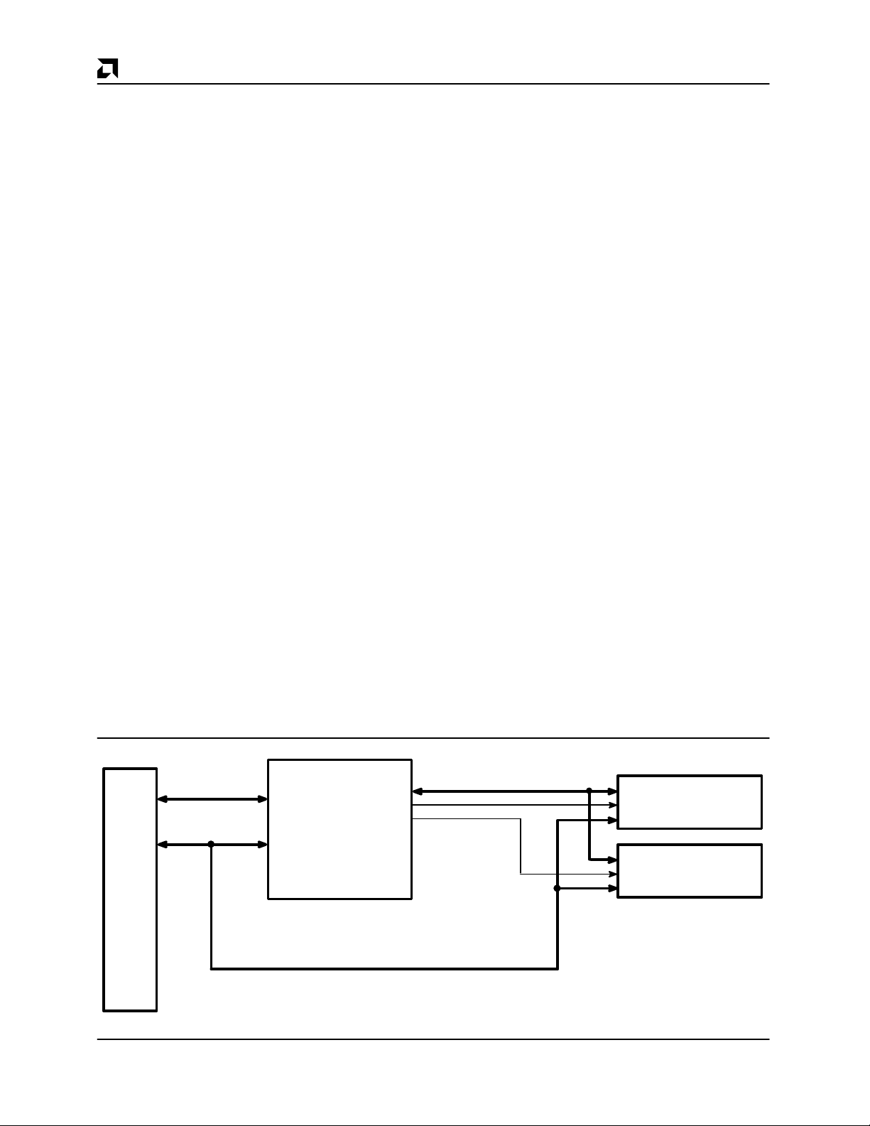
P R E L I M I N A R YAMD
FUNCTIONAL DESCRIPTION
The PCnet-ISA controller is a highly integrated system
solution for the PC-AT ISA architecture. It provides an
Ethernet controller, AUI port, and 10BASE-T transceiver. The PCnet-ISA controller can be directly
interfaced to an ISA system bus. The PCnet-ISA controller contains an ISA bus interface unit, DMA Buffer
Management Unit, 802.3 Media Access Control function, separate 136-byte transmit and 128-byte receive
FIFOs, IEEE defined Attachment Unit Interface (AUI),
and Twisted-Pair Transceiver Media Attachment Unit.
In addition, a Sleep function has been incorporated
which provides low standby current for power sensitive
applications.
The PCnet-ISA controller is register compatible with the
LANCE (Am7990) Ethernet controller and PCnet-ISA
controller (Am79C961). The DMA Buffer Management
Unit supports the LANCE descriptor software model and
the PCnet-ISA controller is software compatible with the
Novell NE2100 and NE1500T add-in cards.
External remote boot and Ethernet physical address
PROMs are supported. The location of the I/O registers
and PROMs are configured by selected pins and internal address comparators (in bus master mode) or
external logic (in shared memory mode).
The PCnet-ISA controller’s bus master architecture
brings to system manufacturers (adapter card and
motherboard makers alike) something they have not
been able to enjoy with other architectures—a low-cost
system solution that provides the lowest parts count and
highest performance. As a bus-mastering device, costly
and power-hungry external SRAMs are not needed for
packet buffering. This results in lower system cost due
to fewer components, less real-estate and less power.
The PCnet-ISA controller’s advanced bus mastering architecture also provides high data throughput and low
CPU utilization for even better performance.
To offer greater flexibility, the PCnet-ISA controller has
a shared memory mode to meet varying application
needs. The shared memory architecture is compatible
with very low-end machines, such as PC/XTs that do not
support bus mastering, and very high end machines
which require local packet buffering for increased system latency.
The network interface provides an Attachment Unit Interface and Twisted-Pair Transceiver functions. Only
one interface is active at any particular time. The AUI
allows for connection via isolation transformer to
10BASE5 and 10BASE2, thick and thin based coaxial
cables. The Twisted-Pair Transceiver interface allows
for connection of unshielded twisted-pair cables as
specified by the Section 14 supplement to IEEE 802.3
Standard (Type 10BASE-T).
Bus Master Mode
+
System Interface
The PCnet-ISA controller has two fundamental operating modes, Bus Master and Shared Memory. The
selection of either the Bus Master mode or the Shared
Memory mode must be done through hard wiring; it is
not software configurable. The Bus Master mode provides an Am7990 (LANCE) compatible Ethernet
controller, an Ethernet Address PROM, a Boot PROM,
and a set of device configuration registers.
The optional Boot PROM is in memory address space
and is expected to be 16 kilobytes or less in size. The
memory address is always related to the I/O address.
For example, 0x300 is always associated with 0xC8000.
On-chip address comparators control device selection
based on the value of the input pins IOAM0 and IOAM1.
The SMEMR input pin can be left unconnected for applications where a Remote Boot PROM is not needed.
The address PROM, board configuration registers, and
the Ethernet controller occupy 24 bytes of I/O space and
can be located on four different starting addresses.
Data buffers are located in motherboard memory and
can be accessed by the PCnet-ISA controller when the
device becomes the Current Master.
16-Bit System Data
ISA
Bus
24-Bit System
Address
SD0–15
PCnet-ISA
Controller
SA0–19
LA17–23
PRDB0–7
APCS
BPCS
Bus Master Block Diagram
1-372 Am79C960
8-Bit Private Data
D0–7
CS
A0–X
D0–7
CS
A0–X
Ethernet
Address
PROM
Boot
PROM
16907B-5
Page 31

P R E L I M I N A R Y AMD
Shared Memory Mode
System Interface
The Shared Memory mode is the other fundamental operating mode available on the PCnet-ISA controller. The
PCnet-ISA controller uses the same descriptor and
buffer architecture as the LANCE, but these data structures are stored in static RAM controlled by the
PCnet-ISA controller. The static RAM is visible as a
memory resource to the PC. The other resources look
the same as in the Bus Master mode.
The Boot PROM is selected by an external device which
drives the Boot PROM Address Match (BPAM) input to
the PCnet-ISA controller. The PCnet-ISA controller can
perform two 8-bit accesses from the 8-bit Boot PROM
and present16-bits of data. The shared memory works
the same way, with an external device generating
Shared Memory Address Match and the PCnet-ISA
controller performing the read or write and the 8 to 16-bit
data conversion.
Converting shared memory accesses from 8-bit cycles
to 16-bit cycles allows use of the much faster 16-bit cycle timing while cutting the number of bus cycles in half.
This raises performance to more than 400% of what
could be achieved with 8-bit cycles. Converting boot
PROM accesses to 16-bit cycles allows the two memory
resources to be in the same 128 Kbyte block of memory
without a clash between two devices with different data
widths.
Note that the external address buffer must drive all the
bits of PRAB10-15 even if the static RAM is less than
64 Kbytes. The PCnet-ISA controller uses an internal
address comparator to perform SRAM prefetches on
the Private Data Bus; the PRAB0-15 signals are used internally to determine whether a SRAM read cycle
prefetch is a match or a miss.
Access to the Ethernet controller registers, board configuration registers, and Address PROM is done with
on-chip address comparators.
Network Interface
The PCnet-ISA controller can be connected to an IEEE
802.3 network via one of two network interface ports.
The Attachment Unit Interface (AUI) provides an
IEEE 802.3 compliant differential interface to a remote
MAU or a transceiver on the system board. The
10BASE-T interface provides a twisted-pair Ethernet
port. The PCnet-ISA controller provides three modes of
network interface selection: automatic selection, software selection, and jumper selection of AUI or
10BASE-T interface.
In the automatic selection mode, the PCnet-ISA controller will select the interface that is connected to the
network by checking the Link Status state machine. If
both AUI and 10BASE-T interfaces are connected, the
10BASE-T interface is selected over AUI. If the
PCnet-ISA controller is initialized for software selection
of network interface, it will read the PORTSEL [1:0] bits
in the Mode register (CSR15.8 and CSR15.7) to determine which interface needs to be activated. For jumper
selection of the network interface, the MAUSEL pin is
used. When the XMAUSEL bit in ISACSR2 is set, a
HIGH on the pin will select the 10BASE-T interface, and
a LOW on the pin will select the AUI interface.
16-Bit System Data
ISA
Bus
System
Address
PRAB0–15
PCnet-ISA
Controller
ABOE BPAM SMAM
E
Address
Buffer
Address
Compare
Shared Memory Block Diagram
PRDB0–7
APCS
SROE
BPCS
SRWE
16-Bit Private Address Bus
8-Bit Private Data
A0–X
CS
D0–7
A0–X
D0–7
OE
WE
A0–X
D0–7
CS
Ethernet
Address
PROM
8-Bit
SRAM
CS
Boot
PROM
OE
16907B-6
Am79C960
1-373
Page 32

P R E L I M I N A R YAMD
DETAILED FUNCTIONS
Bus Interface Unit (BIU)
The bus interface unit is a mixture of a 20 MHz state machine and asynchronous logic. It handles two types of
accesses: accesses where the PCnet-ISA controller is
a slave and accesses where the PCnet-ISA controller is
the Current Master.
In slave mode, signals like IOCS16 are asserted and
deasserted as soon as the appropriate inputs are received. IOCHRDY is asynchronously driven LOW if the
PCnet-ISA controller needs a wait state. It is released
synchronously when the PCnet-ISA controller is ready.
When the PCnet-ISA controller is the Current Master, all
the signals it generates are synchronous to the on-chip
20 MHz clock.
DMA Transfers
The BIU will initiate DMA transfers according to the type
of operation being performed. There are three primary
types of DMA transfers:
1. Initialization Block DMA Transfers
Once the BIU has been granted bus mastership, it will
perform four data transfer cycles (eight bytes) before relinquishing the bus. The four transfers within the
mastership period will always be read cycles to contiguous addresses. There are 12 words to transfer so there
will be three bus mastership periods.
2. Descriptor DMA Transfers
Once the BIU has been granted bus mastership, it will
perform the appropriate number of data transfer cycles
before relinquishing the bus. The transfers within the
mastership period will always be of the same type
(either all read or all write), but may be to noncontiguous addresses. Only the bytes which need to be
read or written are accessed.
3. Burst-Cycle DMA Transfers
Once the BIU has been granted bus mastership, it will
perform a series of consecutive data transfer cycles before relinquishing the bus. Each data transfer will be
performed sequentially, with the issue of the address,
and the transfer of the data with appropriate output signals to indicate selection of the active data bytes during
the transfer. All transfers within the mastership cycle will
be either read or write cycles, and will be to contiguous
addresses. The number of data transfer cycles within
the burst is dependent on the programming of the
DMAPLUS option (CSR4, bit 14).
If DMAPLUS = 0, a maximum of 16 transfers will be performed. This may be changed by writing to the burst
register (CSR80), but the default takes the same
amount of time as the Am2100 family of LANCE-based
boards, a little over 5 microseconds.
If DMAPLUS = 1, the burst will continue until the FIFO is
filled to its high threshold (32 bytes in transmit operation) or emptied to its low threshold (16 bytes in receive
operation). The exact number of transfer cycles in this
case will be dependent on the latency of the system bus
to the BIU’s mastership request and the speed of bus
operation.
Buffer Management Unit (BMU)
The buffer management unit is a micro-coded 20 MHz
state machine which implements the initialization block
and the descriptor architecture.
Initialization
PCnet-ISA controller initialization includes the reading
of the initialization block in memory to obtain the operating parameters. The initialization block is read when the
INIT bit in CSR0 is set. The INIT bit should be set before
or concurrent with the STRT bit to insure correct operation. Four words at a time are read and the bus is
released at the end of each block of reads, for a total of
three arbitration cycles. Once the initialization block has
been read in and processed, the BMU knows where the
receive and transmit descriptor rings are. On completion
of the read operation and after internal registers have
been updated, IDON will be set in CSR0, and an interrupt generated if IENA is set.
The Initialization Block is vectored by the contents of
CSR1 (least significant 16 bits of address) and CSR2
(most significant 8 bits of address). The block contains
the user defined conditions for PCnet-ISA controller operation, together with the address and length
information to allow linkage of the transmit and receive
descriptor rings.
There is an alternative method to initialize the
PCnet-ISA controller. Instead of initialization via the
initialization block in memory, data can be written directly into the appropriate registers. Either method may
be used at the discretion of the programmer. If the registers are written to directly, the INIT bit must not be set, or
the initialization block will be read in, thus overwriting
the previously written information. Please refer to
Appendix C for details on this alternative method.
Reinitialization
The transmitter and receiver section of the PCnet-ISA
controller can be turned on via the initialization block
(MODE Register DTX, DRX bits CSR15[1:0]). The state
of the transmitter and receiver are monitored through
CSR0 (RXON, TXON bits). The PCnet-ISA controller
should be reinitialized if the transmitter and/or the receiver were not turned on during the original initialization
and it was subsequently required to activate them, or if
either section shut off due to the detection of an error
condition (MERR, UFLO, TX BUFF error).
Reinitialization may be done via the initialization block or
by setting the STOP bit in CSR0, followed by writing to
CSR15, and then setting the START bit in CSR0. Note
that this form of restart will not perform the same in the
PCnet-ISA controller as in the LANCE. In particular, the
PCnet-ISA controller reloads the transmit and receive
descriptor pointers with their respective base ad-
1-374 Am79C960
Page 33

P R E L I M I N A R Y AMD
dresses. This means that the software must clear the
descriptor own bits and reset its descriptor ring pointers
before the restart of the PCnet-ISA controller. The
reload of descriptor base addresses is performed in the
LANCE only after initialization, so a restart of the
LANCE without initialization leaves the LANCE pointing
at the same descriptor locations as before the restart.
Buffer Management
Buffer management is accomplished through message
descriptor entries organized as ring structures in memory. There are two rings, a receive ring and a transmit
ring. The size of a message descriptor entry is 4 words
(8 bytes).
Descriptor Rings
Each descriptor ring must be organized in a contiguous
area of memory. At initialization time (setting the INIT bit
in CSR0), the PCnet-ISA controller reads the user-defined base address for the transmit and receive
descriptor rings, which must be on an 8-byte boundary,
as well as the number of entries contained in the descriptor rings. By default, a maximum of 128 ring entries
is permitted when utilizing the initialization block, which
uses values of TLEN and RLEN to specify the transmit
and receive descriptor ring lengths. However, the ring
lengths can be manually defined (up to 65535) by writing
the transmit and receive ring length registers
(CSR76,78) directly.
■ Status information indicating the condition of
the buffer
Receive descriptor entries are similar (but not identical)
to transmit descriptor entries. Both are composed of four
registers, each 16 bits wide for a total of 8 bytes.
To permit the queuing and de-queuing of message buffers, ownership of each buffer is allocated to either the
PCnet-ISA controller or the host. The OWN bit within the
descriptor status information, either TMD or RMD (see
section on TMD or RMD), is used for this purpose.
“Deadly Embrace” conditions are avoided by the ownership mechanism. Only the owner is permitted to
relinquish ownership or to write to any field in the
descriptor entry. A device that is not the current owner of
a descriptor entry cannot assume ownership or change
any field in the entry.
Descriptor Ring Access Mechanism
At initialization, the PCnet-ISA controller reads the base
address of both the transmit and receive descriptor rings
into CSRs for use by the PCnet-ISA controller during
subsequent operation.
When transmit and receive functions begin, the base
address of each ring is loaded into the current descriptor
address registers and the address of the next descriptor
entry in the transmit and receive rings is computed and
loaded into the next descriptor address registers.
Each ring entry contains the following information:
■ The address of the actual message data buffer
in user or host memory
■ The length of the message buffer
Am79C960
1-375
Page 34

P R E L I M I N A R YAMD
N
RES
24-Bit Base Address
Pointer to
Initialization Block
CSR2
IADR[23:16]
CSR1
IADR[15:0]
N
RCV Descriptor
RX DESCRIPTOR RINGS
1st desc.
start
Ring
N
2nd desc.
start
N
•
•
•
RLEN
TLEN
Initialization
Block
MODE
PADR[15:0]
PADR[31:16]
PADR[47:32]
LADRF[15:0]
LADRF[31:16]
LADRF[47:32]
LADRF[63:48]
RDRA[15:0]
RES
RDRA[23:16]
TDRA[15:0]
TDRA[23:16]
RES
RCV
Buffers
16907B-7
XMT
Buffers
RMD0
RMD1
RMD2
Data
Buffer
1
RX DESCRIPTOR RINGS
RX DESCRIPTOR RINGS
1st desc.
start
TMD0
Data
Buffer
1
Data
Buffer
2
M
XMT Descriptor
Ring
TMD1
TMD2
Data
Buffer
2
M
RMD3
M
TMD3
RMD0
•••
M
2nd desc.
start
TMD0
•••
Data
Buffer
N
•
Data
Buffer
M
•
•
16907B-7
Initialization Block and Descriptor Rings
Polling
When there is no channel activity and there is no pre- or
post-receive or transmit activity being performed by the
PCnet-ISA controller, then the PCnet-ISA controller will
periodically poll the current receive and transmit descriptor entries in order to ascertain their ownership. If
the DPOLL bit in CSR4 is set, then the transmit polling
function is disabled.
A typical polling operation consists of the following: The
will then use the current transmit descriptor address
(stored internally) to vector to the appropriate Transmit
Descriptor Table Entry (TDTE). These accesses will be
made to RMD1 and RMD0 of the current RDTE and
TMD1 and TMD0 of the current TDTE at periodic polling
intervals. All information collected during polling activity
will be stored internally in the appropriate CSRs. (i.e.
CSR18–19, CSR20–21, CSR40, CSR42, CSR50,
CSR52). UnOWNed descriptor status will be internally
ignored.
PCnet-ISA controller will use the current receive descriptor address stored internally to vector to the
appropriate Receive Descriptor Table Entry (RDTE). It
1-376 Am79C960
Page 35

P R E L I M I N A R Y AMD
A typical receive poll occurs under the following
conditions:
1) PCnet-ISA controller does not possess ownership
of the current RDTE and
the poll time has elapsed and
RXON = 1,
or
2) PCnet-ISA controller does not possess ownership
of the next RDTE and
the poll time has elapsed and
RXON = 1.
If RXON = 0, the PCnet-ISA controller will never poll
RDTE locations.
If RXON=1, the system should always have at least one
RDTE available for the possibility of a receive event.
When there is only one RDTE, there is no polling for next
RDTE.
A typical transmit poll occurs under the following
conditions:
1) PCnet-ISA controller does not possess ownership
of the current TDTE and
DPOLL = 0 and
TXON = 1 and
the poll time has elapsed,
or
2) PCnet-ISA controller does not possess ownership
of the current TDTE and
DPOLL = 0 and
TXON = 1 and
a packet has just been received,
or
3) PCnet-ISA controller does not possess ownership
of the current TDTE and
DPOLL = 0 and
TXON = 1 and
a packet has just been transmitted.
The poll time interval is nominally defined as 32,768
crystal clock periods, or 1.6 ms. However, the poll time
register is controlled internally by microcode, so any
other microcode controlled operation will interrupt the
incrementing of the poll count register. For example,
when a receive packet is accepted by the PCnet-ISA
controller, the device suspends execution of the polltime-incrementing microcode so that a receive
microcode routine may instead be executed. Poll-timeincrementing code is resumed when the receive
operation has completely finished. Note, however, that
following the completion of any receive or transmit operation, a poll operation will always be performed. The
poll time count register is never reset. Note that if a nondefault value is desired, then a strict sequence of setting
the INIT bit in CSR0, waiting for INITDONE, then writing
to CSR47, and then setting STRT in CSR0 must be observed, otherwise the default value will not be
overwritten. See the CSR47 section for details.
Setting the TDMD bit of CSR0 will cause the microcode
controller to exit the poll counting code and immediately
perform a polling operation. If RDTE ownership has not
been previously established, then an RDTE poll will be
performed ahead of the TDTE poll.
Transmit Descriptor Table Entry (TDTE)
If, after a TDTE access, the PCnet-ISA controller finds
that the OWN bit of that TDTE is not set, then the
PCnet-ISA controller resumes the poll time count and
reexamines the same TDTE at the next expiration of the
poll time count.
If the OWN bit of the TDTE is set, but STP = 0, the
PCnet-ISA controller will immediately request the bus in
order to reset the OWN bit of this descriptor; this condi-
tion would normally be found following a LCOL or
RETRY error that occurred in the middle of a transmit
packet chain of buffers. After resetting the OWN bit of
this descriptor, the PCnet-ISA controller will again im-
mediately request the bus in order to access the next
TDTE location in the ring.
If the OWN bit is set and the buffer length is 0, the OWN
bit will be reset. In the LANCE the buffer length of 0 is
interpreted as a 4096-byte buffer. It is acceptable to
have a 0 length buffer on transmit with STP = 1 or STP =
and
ENP = 1. It is not acceptable to have 0 length
1
buffer with STP = 0
and
ENP = 1.
If the OWN bit is set and the start of packet (STP) bit is
set, then microcode control proceeds to a routine that
will enable transmit data transfers to the FIFO.
If the transmit buffers are data chained (ENP=0 in the
first buffer), then the PCnet-ISA controller will look
ahead to the next transmit descriptor after it has per-
formed at least one transmit data transfer from the first
buffer. More than one transmit data transfer may possi-
bly take place, depending upon the state of the
transmitter. The transmit descriptor lookahead reads
TMD0 first and TMD1 second. The contents of TMD0
and TMD1 will be stored in Next TX Descriptor Address
(CSR32), Next TX Byte Count (CSR66) and Next TX
Status (CSR67) regardless of the state of the OWN bit.
This transmit descriptor lookahead operation is per-
formed only once.
If the PCnet-ISA controller does not own the next TDTE
(i.e. the second TDTE for this packet), then it will com-
plete transmission of the current buffer and then update
the status of the current (first) TDTE with the BUFF and
UFLO bits being set. This will cause the transmitter to be
disabled (CSR0, TXON = 0). The PCnet-ISA controller
will have to be restarted to restore the transmit function.
The situation that matches this description implies that
the system has not been able to stay ahead of the
PCnet-ISA controller in the transmit descriptor ring and,
therefore, the condition is treated as a fatal error. To
avoid this situation, the system should always set the
transmit chain descriptor own bits in reverse order.
Am79C960
1-377
Page 36

P R E L I M I N A R YAMD
If the PCnet-ISA controller does own the second TDTE
in a chain, it will gradually empty the contents of the first
buffer (as the bytes are needed by the transmit operation), perform a single-cycle DMA transfer to update the
status (reset the OWN bit in TMD1) of the first
descriptor, and then it may perform one data DMA access on the second buffer in the chain before executing
another lookahead operation. (i.e. a lookahead to the
third descriptor.)
The PCnet-ISA controller can queue up to two packets
in the transmit FIFO. Call them packet “X” and packet
“Y”, where “Y” is after “X”. Assume that packet “X” is
currently being transmitted. Because the PCnet-ISA
controller can perform lookahead data transfer over an
ENP, it is possible for the PCnet-ISA controller to update
a TDTE in a buffer belonging to packet “Y” while packet
“X” is being transmitted if packet “Y” uses data chaining.
This operation will result in non-sequential TDTE accesses as packet “X” completes transmission and the
PCnet-ISA controller writes out its status, since packet
“X”’s TDTE is before the TDTE accessed as part of the
lookahead data transfer from packet “Y”.
This should not cause any problem for properly written
software which processes buffers in sequence, waiting
for ownership before proceeding.
If an error occurs in the transmission before all of the
bytes of the current buffer have been transferred, then
TMD2 and TMD1 of the current buffer will be written; in
that case, data transfers from the next buffer will not
commence. Instead, following the TMD2/TMD1 update,
the PCnet-ISA controller will go to the next transmit
packet, if any, skipping over the rest of the packet which
experienced an error, including chained buffers.
This is done by returning to the polling microcode where
it will immediately access the next descriptor and find
the condition OWN = 1 and STP = 0 as described earlier.
In that case, the PCnet-ISA controller will reset the own
bit for this descriptor and continue in like manner until a
descriptor with OWN = 0 (no more transmit packets in
the ring) or OWN = 1 and STP = 1 (the first buffer of a
new packet) is reached.
At the end of any transmit operation, whether successful
or with errors, and the completion of the descriptor updates, the PCnet-ISA controller will always perform
another poll operation. As described earlier, this poll operation will begin with a check of the current RDTE,
unless the PCnet-ISA controller already owns that descriptor. Then the PCnet-ISA controller will proceed to
polling the next TDTE. If the transmit descriptor OWN bit
has a zero value, then the PCnet-ISA controller will resume poll time count incrementation. If the transmit
descriptor OWN bit has a value of ONE, then the
PCnet-ISA controller will begin filling the FIFO with
transmit data and initiate a transmission. This end-ofoperation poll avoids inserting poll time counts between
successive transmit packets.
Whenever the PCnet-ISA controller completes a transmit packet (either with or without error) and writes the
status information to the current descriptor, then the
TINT bit of CSR0 is set to indicate the completion of a
transmission. This causes an interrupt signal if the IENA
bit of CSR0 has been set and the TINTM bit of CSR3
is reset.
Receive Descriptor Table Entry (RDTE)
If the PCnet-ISA controller does not own both the cur-
rent and the next Receive Descriptor Table Entry, then
the PCnet-ISA controller will continue to poll according
to the polling sequence described above. If the receive
descriptor ring length is 1, there is no next descriptor,
and no look ahead poll will take place.
If a poll operation has revealed that the current and the
next RDTE belongs to the PCnet-ISA controller, then
additional poll accesses are not necessary. Future poll
operations will not include RDTE accesses as long as
the PCnet-ISA controller retains ownership to the cur-
rent and the next RDTE.
When receive activity is present on the channel, the
PCnet-ISA controller waits for the complete address of
the message to arrive. It then decides whether to accept
or reject the packet based on all active addressing
schemes. If the packet is accepted the PCnet-ISA con-
troller checks the current receive buffer status register
CRST (CSR40) to determine the ownership of the cur-
rent buffer.
If ownership is lacking, then the PCnet-ISA controller
will immediately perform a (last ditch) poll of the current
RDTE. If ownership is still denied, then the PCnet-ISA
controller has no buffer in which to store the incoming
message. The MISS bit will be set in CSR0 and an inter-
rupt will be generated if IENA = 1 (CSR0) and
MISSM = 0 (CSR3). Another poll of the current RDTE
will not occur until the packet has finished.
If the PCnet-ISA controller sees that the last poll (either
a normal poll or the last-ditch effort described in the
above paragraph) of the current RDTE shows valid own-
ership, then it proceeds to a poll of the next RDTE.
Following this poll, and regardless of the outcome of this
poll, transfers of receive data from the FIFO may begin.
Regardless of ownership of the second receive descrip-
tor, the PCnet-ISA controller will continue to perform
receive data DMA transfers to the first buffer, using
burst-cycle DMA transfers. If the packet length exceeds
the length of the first buffer, and the PCnet-ISA control-
ler does not own the second buffer, ownership of the
current descriptor will be passed back to the system by
writing a zero to the OWN bit of RMD1 and status will be
written indicating buffer (BUFF = 1) and possibly over-
flow (OFLO = 1) errors.
If the packet length exceeds the length of the first (cur-
rent) buffer, and the PCnet-ISA controller does own the
second (next) buffer, ownership will be passed back to
the system by writing a zero to the OWN bit of RMD1
when the first buffer is full. Receive data transfers to the
second buffer may occur before the PCnet-ISA control-
ler proceeds to look ahead to the ownership of the third
buffer. Such action will depend upon the state of the
FIFO when the status has been updated on the first de-
1-378 Am79C960
Page 37

P R E L I M I N A R Y AMD
scriptor. In any case, lookahead will be performed to the
third buffer and the information gathered will be stored in
the chip, regardless of the state of the ownership bit. As
in the transmit flow, lookahead operations are performed only once.
This activity continues until the PCnet-ISA controller
recognizes the completion of the packet (the last byte of
this receive message has been removed from the
FIFO). The PCnet-ISA controller will subsequently
update the current RDTE status with the end of packet
(ENP) indication set, write the message byte count
(MCNT) of the complete packet into RMD2 and overwrite the “current” entries in the CSRs with the
“next” entries.
Media Access Control
The Media Access Control engine incorporates the essential protocol requirements for operation of a
compliant Ethernet/802.3 node, and provides the interface between the FIFO sub-system and the Manchester
Encoder/Decoder (MENDEC).
The MAC engine is fully compliant to Section 4 of ISO/
IEC 8802-3 (ANSI/IEEE Standard 1990 Second Edition)
and ANSI/IEEE 802.3 (1985).
The MAC engine provides programmable enhanced
features designed to minimize host supervision and pre
or post-message processing. These features include
the ability to disable retries after a collision, dynamic
FCS generation on a packet-by-packet basis, and automatic pad field insertion and deletion to enforce
minimum frame size attributes.
The two primary attributes of the MAC engine are:
■ Transmit and receive message data encapsulation
— Framing (frame boundary delimitation, frame
synchronization)
— Addressing (source and destination address
handling)
— Error detection (physical medium transmission
errors)
■ Media access management
— Medium allocation (collision avoidance)
— Contention resolution (collision handling)
Transmit And Receive Message Data
Encapsulation
The MAC engine provides minimum frame size enforcement for transmit and receive packets. When
APAD_XMT = 1 (bit 11 in CSR4), transmit messages
will be padded with sufficient bytes (containing 00h) to
ensure that the receiving station will observe an information field (destination address, source address,
length/type, data and FCS) of 64 bytes. When
ASTRP_RCV = 1 (bit 10 in CSR4), the receiver will automatically strip pad bytes from the received message by
observing the value in the length field, and stripping excess bytes if this value is below the minimum data size
(46 bytes). Both features can be independently over-
ridden to allow illegally short (less than 64 bytes of
packet data) messages to be transmitted and/
or received.
Framing (Frame Boundary Delimitation, Frame
Synchronization)
The MAC engine will autonomously handle the con-
struction of the transmit frame. Once the Transmit FIFO
has been filled to the predetermined threshold (set by
XMTSP in CSR80), and providing access to the channel
is currently permitted, the MAC engine will commence
the 7-byte preamble sequence (10101010b, where first
bit transmitted is a 1). The MAC engine will subse-
quently append the Start Frame Delimiter (SFD) byte
(10101011b) followed by the serialized data from the
Transmit FIFO. Once the data has been completed, the
MAC engine will append the FCS (most significant bit
first) which was computed on the entire data portion of
the message.
Note that the user is responsible for the correct ordering
and content in each of the fields in the frame, including
the destination address, source address, length/type
and packet data.
The receive section of the MAC engine will detect an in-
coming preamble sequence and lock to the encoded
clock. The internal MENDEC will decode the serial bit
stream and present this to the MAC engine. The MAC
will discard the first 8 bits of information before search-
ing for the SFD sequence. Once the SFD is detected, all
subsequent bits are treated as part of the frame. The
MAC engine will inspect the length field to ensure mini-
mum frame size, strip unnecessary pad characters (if
enabled), and pass the remaining bytes through the Re-
ceive FIFO to the host. If pad stripping is performed, the
MAC engine will also strip the received FCS bytes, al-
though the normal FCS computation and checking will
occur. Note that apart from pad stripping, the frame will
be passed unmodified to the host. If the length field has
a value of 46 or greater, the MAC engine will not attempt
to validate the length against the number of bytes con-
tained in the message.
If the frame terminates or suffers a collision before
64 bytes of information (after SFD) have been received,
the MAC engine will automatically delete the frame from
the Receive FIFO, without host intervention.
Addressing (Source and Destination Address
Handling)
The first 6 bytes of information after SFD will be inter-
preted as the destination address field. The MAC engine
provides facilities for physical, logical, and broadcast
address reception. In addition, multiple physical ad-
dresses can be constructed (perfect address filtering)
using external logic in conjunction with the EADI
interface.
Error Detection (Physical Medium Transmission
Errors)
The MAC engine provides several facilities which report
and recover from errors on the medium. In addition, the
Am79C960
1-379
Page 38

P R E L I M I N A R YAMD
network is protected from gross errors due to inability of
the host to keep pace with the MAC engine activity.
On completion of transmission, the following transmit
status is available in the appropriate TMD and CSR
areas:
■ The exact number of transmission retry attempts
(ONE, MORE, or RTRY)
■ Whether the MAC engine had to Defer (DEF)
due to channel activity
■ Loss of Carrier, indicating that there was an
interruption in the ability of the MAC engine to
monitor its own transmission. Repeated LCAR
errors indicate a potentially faulty transceiver
or network connection.
■ Late Collision (LCOL) indicates that the
transmission suffered a collision after the slot time.
This is indicative of a badly configured network.
Late collisions should not occur in a normal
operating network.
■ Collision Error (CERR) indicates that the
transceiver did not respond with an SQE Test
message within the predetermined time after a
transmission completed. This may be due to a
failed transceiver, disconnected or faulty transceiver drop cable, or the fact the transceiver does
not support this feature (or the feature is disabled).
In addition to the reporting of network errors, the MAC
engine will also attempt to prevent the creation of any
network error due to the inability of the host to service
the MAC engine. During transmission, if the host fails to
keep the Transmit FIFO filled sufficiently, causing an underflow, the MAC engine will guarantee the message is
either sent as a runt packet (which will be deleted by the
receiving station) or has an invalid FCS (which will also
cause the receiver to reject the message).
The status of each receive message is available in the
appropriate RMD and CSR areas. FCS and Framing errors (FRAM) are reported, although the received frame
is still passed to the host. The FRAM error will only be
reported if an FCS error is detected and there are a nonintegral number of bits in the message. The MAC engine
will ignore up to seven additional bits at the end of a
message (dribbling bits), which can occur under normal
network operating conditions. The reception of eight additional bits will cause the MAC engine to de-serialize
the entire byte, and will result in the received message
and FCS being modified.
The PCnet-ISA controller can handle up to 7 dribbling
bits when a received packet terminates. During the reception, the CRC is generated on every serial bit
(including the dribbling bits) coming from the cable, although the internally saved CRC value is only updated
on the eighth bit (on each byte boundary). The framing
error is reported to the user as follows:
1. If the number of the dribbling bits are 1 to 7 and there
is no CRC error, then there is no Framing error
(FRAM = 0).
2. If the number of the dribbling bits are less than 8 and
there is a CRC error, then there is also a Framing
error (FRAM = 1).
3. If the number of dribbling bits = 0, then there is no
Framing error. There may or may not be a CRC
(FCS) error.
Counters are provided to report the Receive Collision
Count and Runt Packet Count and used for network sta-
tistics and utilization calculations.
Note that if the MAC engine detects a received packet
which has a 00b pattern in the preamble (after the first
8 bits, which are ignored), the entire packet will be ig-
nored. The MAC engine will wait for the network to go
inactive before attempting to receive the next packet.
Media Access Management
The basic requirement for all stations on the network is
to provide fairness of channel allocation. The
802.3/Ethernet protocol defines a media access mecha-
nism which permits all stations to access the channel
with equality. Any node can attempt to contend for the
channel by waiting for a predetermined time (Inter
Packet Gap interval) after the last activity, before trans-
mitting on the medium. The channel is a multidrop
communications medium (with various topological con-
figurations permitted) which allows a single station to
transmit and all other stations to receive. If two nodes
simultaneously contend for the channel, their signals
will interact, causing loss of data (defined as a collision).
It is the responsibility of the MAC to attempt to avoid and
recover from a collision, to guarantee data integrity for
the end-to-end transmission to the receiving station.
Medium Allocation (Collision Avoidance)
The IEEE 802.3 Standard (ISO/IEC 8802-3 1990) re-
quires that the CSMA/CD MAC monitor the medium
traffic by looking for carrier activity. When carrier is de-
tected the medium is considered busy, and the MAC
should defer to the existing message.
The IEEE 802.3 Standard also allows optional two part
deferral after a receive message.
See ANSI/IEEE Std 802.3-1990 Edition, 4.2.3.2.1:
“Note: It is possible for the PLS carrier sense
indication to fail to be asserted during a collision
on the media. If the deference process simply
times the interpacket gap based on this indication it is possible for a short interFrame gap to
be generated, leading to a potential reception
failure of a subsequent frame. To enhance system robustness the following optional
measures, as specified in 4.2.8, are recom-
1-380 Am79C960
Page 39

P R E L I M I N A R Y AMD
mended when InterFrameSpacingPart1 is
other than zero:
(1) Upon completing a transmission, start timing
the interpacket gap, as soon as transmitting
and carrierSense are both false.
(2) When timing an interpacket gap following re-
ception, reset the interpacket gap timing if
carrier Sense becomes true during the first 2/3
of the interpacket gap timing interval. During the
final 1/3 of the interval the timer shall not be reset to ensure fair access to the medium. An
initial period shorter than 2/3 of the interval is
permissible including zero.”
The MAC engine implements the optional receive two
part deferral algorithm, with a first part inter-frame-spacing time of 6.0 µs. The second part of the
inter-frame-spacing interval is therefore 3.6 µs.
The PCnet-ISA controller will perform the two-part
deferral algorithm as specified in Section 4.2.8 (Process
Deference). The Inter Packet Gap (IPG) timer will start
timing the 9.6 µs InterFrameSpacing after the receive
carrier is de-asserted. During the first part deferral
(InterFrameSpacingPart1 - IFS1) the PCnet-ISA controller will defer any pending transmit frame and respond
to the receive message. The IPG counter will be reset to
zero continuously until the carrier de-asserts, at which
point the IPG counter will resume the 9.6 µs count once
again. Once the IFS1 period of 6.0 µs has elapsed, the
PCnet-ISA controller will begin timing the second part
deferral (InterFrameSpacingPart2 - IFS2) of 3.6 µs.
Once IFS1 has completed, and IFS2 has commenced,
the PCnet-ISA controller will not defer to a receive packet if a transmit packet is pending. This means that the
PCnet-ISA controller will not attempt to receive the receive packet, since it will start to transmit, and generate
a collision at 9.6 µs. The PCnet-ISA controller will guarantee to complete the preamble (64-bit) and jam (32-bit)
sequence before ceasing transmission and invoking the
random backoff algorithm.
In addition, transmit two part deferral is implemented as
an option which can be disabled using the DXMT2PD bit
(CSR3). Two-part deferral after transmission is useful
for ensuring that severe IPG shrinkage cannot occur in
specific circumstances, causing a transmit message to
follow a receive message so closely as to make them
indistinguishable.
During the time period immediately after a transmission
has been completed, the external transceiver (in the
case of a standard AUI connected device), should generate the SQE Test message (a nominal 10 MHz burst of
5-15 Bit Times duration) on the CI± pair (within 0.6 µs –
1.6 µs after the transmission ceases). During the time
period in which the SQE Test message is expected the
PCnet-ISA controller will not respond to receive carrier
sense.
“At the conclusion of the output function, the
DTE opens a time window during which it expects to see the
signal_quality_erro
r signal
asserted on the Control In circuit. The time window begins when the CARRIER_STATUS
becomes CARRIER_OFF. If execution of the
output function does not cause CARRIER_ON
to occur, no SQE test occurs in the DTE. The
µ
duration of the window shall be at least 4.0
s
but no more than 8.0 µs. During the time window the Carrier Sense Function is inhibited.”
The PCnet-ISA controller implements a carrier sense
“blinding” period within 0 – 4.0 µs from deassertion of
carrier sense after transmission. This effectively means
that when transmit two part deferral is enabled
(DXMT2PD is cleared) the IFS1 time is from 4 µs to 6 µs
after a transmission. However, since IPG shrinkage below 4 µs will rarely be encountered on a correctly
configured network, and since the fragment size will be
larger than the 4 µs blinding window, then the IPG
counter will be reset by a worst case IPG shrinkage/fragment scenario and the PCnet-ISA controller will defer its
transmission. In addition, the PCnet-ISA controller will
not restart the “blinding” period if carrier is detected
within the 4.0 µs – 6.0 µs IFS1 period, but will commence timing of the entire IFS1 period.
Contention Resolution (Collision Handling)
Collision detection is performed and reported to the
MAC engine by the integrated Manchester Encoder/
Decoder (MENDEC).
If a collision is detected before the complete preamble/
SFD sequence has been transmitted, the MAC Engine
will complete the preamble/SFD before appending the
jam sequence. If a collision is detected after the preamble/SFD has been completed, but prior to 512 bits being
transmitted, the MAC Engine will abort the transmission, and append the jam sequence immediately. The
jam sequence is a 32-bit all zeroes pattern.
The MAC Engine will attempt to transmit a frame a total
of 16 times (initial attempt plus 15 retries) due to normal
collisions (those within the slot time). Detection of collision will cause the transmission to be re-scheduled,
dependent on the backoff time that the MAC Engine
computes. If a single retry was required, the ONE bit will
be set in the Transmit Frame Status (TMD1 in the Transmit Descriptor Ring). If more than one retry was
required, the MORE bit will be set. If all 16 attempts experienced collisions, the RTRY bit (in TMD2) will be set
(ONE and MORE will be clear), and the transmit message will be flushed from the FIFO. If retries have been
disabled by setting the DRTY bit in the MODE register
(CSR15), the MAC Engine will abandon transmission of
the frame on detection of the first collision. In this case,
only the RTRY bit will be set and the transmit message
will be flushed from the FIFO.
See ANSI/IEEE Std 802.3-1990 Edition,
7.2.4.6 (1)):
If a collision is detected after 512 bit times have been
transmitted, the collision is termed a late collision. The
Am79C960
1-381
Page 40

P R E L I M I N A R YAMD
MAC Engine will abort the transmission, append the jam
sequence, and set the LCOL bit. No retry attempt will be
scheduled on detection of a late collision, and the FIFO
will be flushed.
The IEEE 802.3 Standard requires use of a “truncated
binary exponential backoff” algorithm which provides a
controlled pseudo-random mechanism to enforce the
collision backoff interval, before re-transmission is
attempted.
See ANSI/IEEE Std 802.3-1990 Edition, 4.2.3.2.5:
“At the end of enforcing a collision (jamming),
the CSMA/CD sublayer delays before attempting to re-transmit the frame. The delay is an
integer multiple of slotTime. The number of slot
times to delay before the nth re-transmission
attempt is chosen as a uniformly distributed
random integer r in the range:
≤
r < 2k, where k = min (n,10).”
0
The PCnet-ISA controller provides an alternative algorithm, which suspends the counting of the slot time/IPG
during the time that receive carrier sense is detected.
This algorithm aids in networks where large numbers of
nodes are present, and numerous nodes can be in
collision. The algorithm effectively accelerates the
increase in the backoff time in busy networks, and allows nodes not involved in the collision to access the
channel while the colliding nodes await a reduction in
channel activity. Once channel activity is reduced, the
nodes resolving the collision time out their slot time
counters as normal.
Manchester Encoder/Decoder
(MENDEC)
The integrated Manchester Encoder/Decoder provides
the PLS (Physical Layer Signaling) functions required
for a fully compliant IEEE 802.3 station. The MENDEC
provides the encoding function for data to be transmitted
on the network using the high accuracy on-board oscillator, driven by either the crystal oscillator or an external
CMOS-level compatible clock. The MENDEC also provides the decoding function from data received from the
network. The MENDEC contains a Power On Reset
(POR) circuit, which ensures that all analog portions of
the PCnet-ISA controller are forced into their correct
state during power-up, and prevents erroneous data
transmission and/or reception during this time.
External Crystal Characteristics
When using a crystal to drive the oscillator, the crystal
specification shown in the table may be used to ensure
less than ±0.5 ns jitter at DO±.
Table : External Crystal Characteristics
Min Nom Max UnitsParameter
1.Parallel Resonant
Frequency 20 MHz
2.Resonant Frequency Error
(CL = 20 pF) –50 +50 PPM
3.Change in Resonant Frequency
With Respect To Temperature –40 +40 PPM
(0° – 70° C; CL = 20 pF)*
4.Crystal Capacitance 20 pF
5.Motional Crystal
Capacitance (C1) 0.022 pF
6.Series Resistance 25 Ω
7.Shunt Capacitance 7 pF
8.Drive Level TBD mW
* Requires trimming crystal spec; no trim is 50 ppm total
External Clock Drive Characteristics
When driving the oscillator from an external clock
source, XTAL2 must be left floating (unconnected). An
external clock having the following characteristics must
be used to ensure less than ±0.5 ns jitter at DO±:
Clock Frequency: 20 MHz ±0.01%
Rise/Fall Time (tR/tF): < 6 ns from 0.5 V
to V
XTAL1 HIGH/LOW Time 20 ns min
(tHIGH/tLOW):
XTAL1 Falling Edge to < ±0.2 ns at
Falling Edge Jitter: 2.5 V input (V
DD
–0.5
DD
/2)
MENDEC Transmit Path
The transmit section encodes separate clock and NRZ
data input signals into a standard Manchester encoded
serial bit stream. The transmit outputs (DO±) are designed to operate into terminated transmission lines.
When operating into a 78 Ω terminated transmission
line, the transmit signaling meets the required output
levels and skew for Cheapernet, Ethernet, and
IEEE-802.3.
1-382 Am79C960
Page 41

P R E L I M I N A R Y AMD
Transmitter Timing and Operation
A 20 MHz fundamental-mode crystal oscillator provides
the basic timing reference for the MENDEC portion of
the PCnet-ISA controller. The crystal input is divided by
two to create the internal transmit clock reference. Both
clocks are fed into the Manchester Encoder to generate
the transitions in the encoded data stream. The internal
transmit clock is used by the MENDEC to internally synchronize the Internal Transmit Data (ITXDAT) from the
controller and Internal Transmit Enable (ITXEN). The internal transmit clock is also used as a stable bit-rate
clock by the receive section of the MENDEC and
controller.
The oscillator requires an external 0.005% crystal, or an
external 0.01% CMOS-level input as a reference. The
accuracy requirements, if an external crystal is used,
are tighter because allowance for the on-chip oscillator
must be made to deliver a final accuracy of 0.01%.
Transmission is enabled by the controller. As long as the
ITXEN request remains active, the serial output of the
controller will be Manchester encoded and appear at
DO±. When the internal request is dropped by the controller, the differential transmit outputs go to one of two
idle states, dependent on TSEL in the Mode Register
(CSR15, bit 9):
TSEL LOW: The idle state of DO± yields “zero”
differential to operate transformer-
coupled loads.
TSEL HIGH: In this idle state, DO+ is positive
with respect to DO– (logical HIGH).
Receive Path
The principal functions of the receiver are to signal the
PCnet-ISA controller that there is information on the receive pair, and to separate the incoming Manchester
encoded data stream into clock and NRZ data.
The receiver section (see Receiver Block Diagram) consists of two parallel paths. The receive data path is a
zero threshold, wide bandwidth line receiver. The carrier
path is an offset threshold bandpass detecting line
receiver. Both receivers share common bias networks
to allow operation over a wide input common mode
range.
Input Signal Conditioning
Transient noise pulses at the input data stream are rejected by the Noise Rejection Filter. Pulse width
rejection is proportional to transmit data rate. DC inputs
more negative than minus 100 mV are also suppressed.
The Carrier Detection circuitry detects the presence of
an incoming data packet by discerning and rejecting
noise from expected Manchester data, and controls the
stop and start of the phase-lock loop during clock acquisition. Clock acquisition requires a valid Manchester bit
pattern of 1010b to lock onto the incoming message.
When input amplitude and pulse width conditions are
met at DI±, a clock acquisition cycle is initiated.
Clock Acquisition
When there is no activity at DI± (receiver is idle), the receive oscillator is phase-locked to the internal transmit
clock. The first negative clock transition (bit cell center of
first valid Manchester “0”) after IRXCRS is asserted interrupts the receive oscillator. The oscillator is then
restarted at the second Manchester “0” (bit time 4) and is
phase-locked to it. As a result, the MENDEC acquires
the clock from the incoming Manchester bit pattern in
4 bit times with a “1010” Manchester bit pattern.
ISRDCLK and IRXDAT are enabled 1/4 bit time after
clock acquisition in bit cell 5. IRXDAT is at a HIGH state
when the receiver is idle (no ISRDCLK). IRXDAT however, is undefined when clock is acquired and may
remain HIGH or change to LOW state whenever
ISRDCLK is enabled. At 1/4 bit time through bit cell 5,
the controller portion of the PCnet-ISA controller sees
the first ISRDCLK transition. This also strobes in the incoming fifth bit to the MENDEC as Manchester “1”.
IRXDAT may make a transition after the ISRDCLK rising
edge in bit cell 5, but its state is still undefined. The
Manchester “1” at bit 5 is clocked to IRXDAT output at
1/4 bit time in bit cell 6.
DI±/RXD±
*Internal signal
Data
Receiver
Noise
Reject
Filter
Receiver Block Diagram
Am79C960
Manchester
Decoder
Carrier
Detect
Circuit
IRXDAT*
ISRDCLK
IRXCRS*
16907B-8
1-383
Page 42

P R E L I M I N A R YAMD
PLL Tracking
After clock acquisition, the phase-locked clock is compared to the incoming transition at the bit cell center
(BCC) and the resulting phase error is applied to a correction circuit. This circuit ensures that the
phase-locked clock remains locked on the received signal. Individual bit cell phase corrections of the Voltage
Controlled Oscillator (VCO) are limited to 10% of the
phase difference between BCC and phase-locked
clock. Hence, input data jitter is reduced in ISRDCLK by
10 to 1.
Carrier Tracking and End of Message
The carrier detection circuit monitors the DI± inputs after
IRXCRS is asserted for an end of message. IRXCRS
de-asserts 1 to 2 bit times after the last positive transition on the incoming message. This initiates the end of
reception cycle. The time delay from the last rising edge
of the message to IRXCRS deassert allows the last bit to
be strobed by ISRDCLK and transferred to the controller
section, but prevents any extra bit(s) at the end of
message.
Data Decoding
The data receiver is a comparator with clocked output to
minimize noise sensitivity to the DI±/RXD± inputs. Input
error is less than ± 35 mV to minimize sensitivity to input
rise and fall time. ISRDCLK strobes the data receiver
output at 1/4 bit time to determine the value of the
Manchester bit, and clocks the data out on IRXDAT on
the following ISRDCLK. The data receiver also generates the signal used for phase detector comparison to
the internal MENDEC voltage controlled oscillator
(VCO).
Jitter Tolerance Definition
The MENDEC utilizes a clock capture circuit to align its
internal data strobe with an incoming bit stream. The
clock acquisition circuitry requires four valid bits with the
values 1010b. Clock is phase-locked to the negative
transition at the bit cell center of the second “0” in the
pattern.
Since data is strobed at 1/4 bit time, Manchester transitions which shift from their nominal placement through
1/4 bit time will result in improperly decoded data. With
this as the criteria for an error, a definition of “Jitter Handling” is:
The peak deviation approaching or crossing 1/4
bit cell position from nominal input transition, for
which the MENDEC section will properly decode data.
Attachment Unit Interface (AUI)
The AUI is the PLS (Physical Layer Signaling) to PMA
(Physical Medium Attachment) interface which
connects the DTE to a MAU. The differential interface
provided by the PCnet-ISA controller is fully compliant
with Section 7 of ISO 8802-3 (ANSI/IEEE 802.3).
After the PCnet-ISA controller initiates a transmission, it
will expect to see data “looped-back” on the DI± pair
(when the AUI port is selected). This will internally
generate a “carrier sense”, indicating that the integrity of
the data path to and from the MAU is intact, and that the
MAU is operating correctly. This “carrier sense” signal
must be asserted within sometime before end of transmission. If “carrier sense” does not become active in
response to the data transmission, or becomes inactive
before the end of transmission, the loss of carrier
(LCAR) error bit will be set in the Transmit Descriptor
Ring (TMD3, bit 11) after the packet has been
transmitted.
Differential Input Terminations
The differential input for the Manchester data (DI±) is
externally terminated by two 40.2 Ω ±1% resistors and
one optional common-mode bypass capacitor, as
shown in the Differential Input Termination diagram
below. The differential input impedance, Z
common-mode input impedance, Z
ICM, are specified so
IDF, and the
that the Ethernet specification for cable termination impedance is met using standard 1% resistor terminators.
If SIP devices are used, 39 Ω is the nearest usable
equivalent value. The CI± differential inputs are terminated in exactly the same way as the DI± pair.
AUI Isolation
0.01 µF
to 0.1 µF
Transformer
16907B-9
DI+
PCnet-ISA
DI-
40.2 Ω 40.2 Ω
Differential Input Termination
Collision Detection
A MAU detects the collision condition on the network
and generates a differential signal at the CI± inputs. This
collision signal passes through an input stage which detects signal levels and pulse duration. When the signal is
detected by the MENDEC it sets the ICLSN line HIGH.
The condition continues for approximately 1.5 bit times
after the last LOW-to-HIGH transition on CI±.
1-384 Am79C960
Page 43

P R E L I M I N A R Y AMD
Twisted Pair Transceiver (T-MAU)
The T-MAU implements the Medium Attachment Unit
(MAU) functions for the Twisted Pair Medium, as specified by the supplement to IEEE 802.3 standard (Type
10BASE-T). The T-MAU provides twisted pair driver
and receiver circuits, including on-board transmit digital
predistortion and receiver squelch, and a number of additional features including Link Status indication,
Automatic Twisted Pair Receive Polarity Detection/ Correction and indication, Receive Carrier Sense, Transmit
Active and Collision Present indication.
Twisted Pair Transmit Function
The differential driver circuitry in the TXD± and TXP±
pins provides the necessary electrical driving capability
and the pre-distortion control for transmitting signals
over maximum length Twisted Pair cable, as specified
by the 10BASE-T supplement to the IEEE 802.3 Standard. The transmit function for data output meets the
propagation delays and jitter specified by the standard.
Twisted Pair Receive Function
The receiver complies with the receiver specifications of
the IEEE 802.3 10BASE-T Standard, including noise
immunity and received signal rejection criteria (‘Smart
Squelch’). Signals meeting this criteria appearing at the
RXD± differential input pair are routed to the MENDEC.
The receiver function meets the propagation delays and
jitter requirements specified by the standard. The receiver squelch level drops to half its threshold value
after unsquelch to allow reception of minimum amplitude signals and to offset carrier fade in the event of
worst case signal attenuation conditions.
Note that the 10BASE-T Standard defines the receive
input amplitude at the external Media Dependent Interface (MDI). Filter and transformer loss are not specified.
The T-MAU receiver squelch levels are designed to account for a 1 dB insertion loss at 10 MHz for the type of
receive filters and transformers usually used.
Normal 10BASE-T compatible receive thresholds are
invoked when the LRT bit (CSR15, bit 9) is LOW. When
the LRT bit is set, the Low Receive Threshold option is
invoked, and the sensitivity of the T-MAU receiver is increased. Increasing T-MAU sensitivity allows the use of
lines longer than the 100 m target distance of standard
10BASE-T (assuming typical 24 AWG cable). Increased
receiver sensitivity compensates for the increased signal attenuation caused by the additional cable distance.
However, making the receiver more sensitive means
that it is also more susceptible to extraneous noise, primarily caused by coupling from co-resident services
(crosstalk). For this reason, end users may wish to invoke the Low Receive Threshold option on 4-pair cable
only. Multi-pair cables within the same outer sheath
have lower crosstalk attenuation, and may allow noise
emitted from adjacent pairs to couple into the receive
pair, and be of sufficient amplitude to falsely unsquelch
the T-MAU.
Link Test Function
The link test function is implemented as specified by
10BASE-T standard. During periods of transmit pair inactivity, ’Link beat pulses’ will be periodically sent over
the twisted pair medium to constantly monitor medium
integrity.
When the link test function is enabled (DLNKTST bit in
CSR15 is cleared), the absence of link beat pulses and
receive data on the RXD± pair will cause the TMAU to go
into the Link Fail state. In the Link Fail state, data transmission, data reception, data loopback and the collision
detection functions are disabled and remain disabled
until valid data or greater than 5 consecutive link pulses
appear on the RXD± pair. During Link Fail, the Link
Status (LNKST indicated by LED0) signal is inactive.
When the link is identified as functional, the LNKST signal is asserted, and LED0 output will be activated.
In order to inter-operate with systems which do not implement Link Test, this function can be disabled by
setting the DLNKTST bit. With Link Test disabled, the
Data Driver, Receiver and Loopback functions as well
as Collision Detection remain enabled irrespective of
the presence or absence of data or link pulses on the
RXD± pair. Link Test pulses continue to be sent regardless of the state of the DLNKTST bit.
Polarity Detection and Reversal
The T-MAU receive function includes the ability to invert
the polarity of the signals appearing at the RXD± pair if
the polarity of the received signal is reversed (such as in
the case of a wiring error). This feature allows data packets received from a reverse wired RXD± input pair to be
corrected in the T-MAU prior to transfer to the
MENDEC. The polarity detection function is activated
following reset or Link Fail, and will reverse the receive
polarity based on both the polarity of any previous link
beat pulses and the polarity of subsequent packets with
a valid End Transmit Delimiter (ETD).
When in the Link Fail state, the T-MAU will recognize
link beat pulses of either positive or negative polarity.
Exit from the Link Fail state occurs at the reception of 5–
6 consecutive link beat pulses of identical polarity. On
entry to the Link Pass state, the polarity of the last 5 link
beat pulses is used to determine the initial receive polarity configuration and the receiver is reconfigured to
subsequently recognize only link beat pulses of the previously recognized polarity.
Positive link beat pulses are defined as transmitted signal with a positive amplitude greater than 585 mV
(LRT = HIGH) with a pulse width of 60 ns–200 ns. This
positive excursion may be followed by a negative excursion. This definition is consistent with the expected
received signal at a correctly wired receiver, when a link
beat pulse, which fits the template of Figure 14-12 of the
10BASE-T Standard, is generated at a transmitter and
passed through 100 m of twisted pair cable.
Am79C960
1-385
Page 44

P R E L I M I N A R YAMD
Negative link beat pulses are defined as transmitted signals with a negative amplitude greater than 585 mV with
a pulse width of 60 ns–200 ns. This negative excursion
may be followed by a positive excursion. This definition
is consistent with the expected received signal at a reverse wired receiver, when a link beat pulse which fits
the template of Figure 14–12 in the 10BASE-T Standard
is generated at a transmitter and passed through 100 m
of twisted pair cable.
The polarity detection/correction algorithm will remain
“armed” until two consecutive packets with valid ETD of
identical polarity are detected. When “armed,” the receiver is capable of changing the initial or previous
polarity configuration according to the detected ETD
polarity.
On receipt of the first packet with valid ETD following reset or Link Fail, the T-MAU will use the inferred polarity
information to configure its RXD± input, regardless of its
previous state. On receipt of a second packet with a
valid ETD with correct polarity, the detection/correction
algorithm will “lock-in” the received polarity. If the second (or subsequent) packet is not detected as
confirming the previous polarity decision, the most recently detected ETD polarity will be used as the default.
Note that packets with invalid ETD have no effect on updating the previous polarity decision. Once two
consecutive packets with valid ETD have been received, the T-MAU will lock the correction algorithm until
either a Link Fail condition occurs or RESET is asserted.
During polarity reversal, an internal POL signal will be
active. During normal polarity conditions, this internal
POL signal is inactive. The state of this signal can be
read by software and/or displayed by LED when enabled by the LED control bits in the ISA Bus
Configuration Registers (ISACSR5, 6, 7).
Twisted Pair Interface Status
Three signals (XMT, RCV and COL) indicate whether
the T-MAU is transmitting, receiving, or in a collision
state. These signals are internal signals and the behavior of the LED outputs depends on how the LED output
circuitry is programmed.
The T-MAU will power up in the Link Fail state and the
normal algorithm will apply to allow it to enter the Link
Pass state. In the Link Pass state, transmit or receive
activity will be indicated by assertion of RCV signal going active. If T-MAU is selected using the PORTSEL bits
in CSR15 or MAUSEL pin, then when moving from AUI
to T-MAU selection the T-MAU will be forced into the
Link Fail state.
In the Link Fail state, XMT, RCV and COL are inactive.
Collision Detect Function
Activity on both twisted pair signals RXD± and TXD±
constitutes a collision, thereby causing the COL signal
to be asserted. (COL is used by the LED control circuits.) The COL will remain asserted until one of the two
colliding signals changes from active to idle. During collision condition, data presented on the DI± pair will be
sourced from the RXD± input. COL stays active for two
bit times at the end of a collision.
Signal Quality Error (SQE) Test
(Heartbeat) Function
The SQE function is disabled when the 10BASE-T port
is selected and in Link Fail state.
Jabber Function
The Jabber function inhibits the twisted pair transmit
function of the T-MAU if theTXD± circuit is active for an
excessive period (20–150 ms). This prevents any one
node from disrupting the network due to a ‘stuck-on’ or
faulty transmitter. If this maximum transmit time is exceeded, the T-MAU transmitter circuitry is disabled, the
JAB bit is set (CSR4, bit 1), and COL signal asserted.
Once the transmit data stream to the T-MAU is removed, an “unjab” time of 250–750 ms will elapse
before the T-MAU deasserts COL and re-enables the
transmit circuitry.
Power Down
The T-MAU circuitry can be made to go into low power
mode. This feature is useful in battery powered or low
duty cycle systems. The T-MAU will go into power down
mode when RESET is active, coma mode is active, or
the T-MAU is not selected. Refer to the Power Down
Mode section for a description of the various power
down modes.
Any of the three conditions listed above resets the internal logic of the T-MAU and places the device into power
down mode. In this mode, the Twisted Pair driver pins
(TXD±,TXP±) are asserted LOW, and the internal TMAU status signals (LNKST, RCVPOL, XMT, RCV and
COLLISION) are inactive.
Once the SLEEP pin is deasserted, the T-MAU will be
forced into the Link Fail state. The T-MAU will move to
the Link Pass state only after 5 - 6 link beat pulses and/or
a single received message is detected on the RXD±
pair.
In snooze mode, the T-MAU receive circuitry will remain
enabled even while the SLEEP pin is driven LOW.
The T-MAU circuitry will always go into power down
mode if RESET is asserted, coma mode is enabled, or
the T-MAU is not selected.
1-386 Am79C960
Page 45

P R E L I M I N A R Y AMD
EADI (External Address Detection
Interface)
This interface is provided to allow external address filtering. It is selected by setting the EADISEL bit in
ISACSR2. This feature is typically utilized for terminal
servers, bridges and/or router type products. The use of
external logic is required to capture the serial bit stream
from the PCnet-ISA controller, compare it with a table of
stored addresses or identifiers, and perform the desired
function.
The EADI interface operates directly from the NRZ decoded data and clock recovered by the Manchester
decoder or input to the GPSI, allowing the external address detection to be performed in parallel with frame
reception and address comparison in the MAC Station
Address Detection (SAD) block.
SRDCLK is provided to allow clocking of the receive bit
stream into the external address detection logic.
SRDCLK runs only during frame reception activity.
Once a received frame commences and data and clock
are available, the EADI logic will monitor the alternating
(“1,0”) preamble pattern until the two ones of the Start
Frame Delimiter (“1,0,1,0,1,0,1,1”) are detected, at
which point the SF/BD output will be driven HIGH.
After SF/BD is asserted the serial data from SRD should
be de-serialized and sent to a content addressable
memory (CAM) or other address detection device.
To allow simple serial to parallel conversion, SF/BD is
provided as a strobe and/or marker to indicate the delineation of bytes, subsequent to the SFD. This provides
a mechanism to allow not only capture and/or decoding
of the physical or logical (group) address, it also facilitates the capture of header information to determine
protocol and or inter-networking information. The EAR
pin is driven LOW by the external address comparison
logic to reject the frame.
If an internal address match is detected by comparison
with either the Physical or Logical Address field, the
frame will be accepted regardless of the condition of
EAR. Incoming frames which do not pass the internal
address comparison will continue to be received. This
allows approximately 58 byte times after the last destination address bit is available to generate the EAR
signal, assuming the device is not configured to accept
runt packets. EAR will be ignored after 64 byte times after the SFD, and the frame will be accepted if EAR has
not been asserted before this time. If Runt Packet Accept is configured, the EAR signal must be generated
prior to the receive message completion, which could be
as short as 12 byte times (assuming 6 bytes for source
address, 2 bytes for length, no data, 4 bytes for FCS) after the last bit of the destination address is available.
EAR must have a pulse width of at least 200 ns.
Note that setting the PROM bit (CSR15, bit 15) will
cause all receive frames to be received, regardless of
the state of the EAR input.
If the DRCVPA bit (CSR15.13) is set and the logical
address (LADRF) is set to zero, only frames which are
not rejected by EAR will be received.
The EADI interface will operate as long as the STRT bit
in CSR0 is set, even if the receiver and/or transmitter
are disabled by software (DTX and DRX bits in CSR15
set). This situation is useful as a power down mode in
that the PCnet-ISA controller will not perform any DMA
operations; this saves power by not utilizing the ISA bus
driver circuits. However, external circuitry could still respond to specific frames on the network to facilitate
remote node control.
The table below summarizes the operation of the EADI
features.
Table: Internal/External Address Recognition Capabilities
PROM EAR Required Timing Received Messages
1 X No timing requirements All Received Frames
0 1 No timing requirements All Received Frames
0 0 Low for 200 ns within 512 bits after SFD Physical/Logical Matches
Am79C960
1-387
Page 46

P R E L I M I N A R YAMD
General Purpose Serial Interface (GPSI)
The PCnet-ISA controller contains a General Purpose
Serial Interface (GPSI) designed for testing the digital
portions of the chip. The MENDEC, AUI, and twisted
pair interface are by-passed once the device is set up in
the special “test mode” for accessing the GPSI functions. Although this access is intended only for testing
the device, some users may find the non-encoded data
functions useful in some special applications. Note,
however, that the GPSI functions can be accessed only
when the PCnet-ISA devices operate as a bus master.
The PCnet-ISA GPSI signals are consistent with the
LANCE digital serial interface. Since the GPSI functions
can be accessed only through a special test mode, expect some loss of functionality to the device when the
GPSI is invoked. The AUI and 10BASE-T analog interfaces are disabled along with the internal MENDEC
logic. The LA (unlatched address) pins are removed and
To invoke the GPSI signals, follow the procedure below:
1. After reset or I/O read of Reset Address, write 10b
to PORTSEL bits in CSR15.
2. Set the ENTST bit in CSR4
3. Set the GPSIEN bit in CSR124 (see note below)
(The pins LA17–LA23 will change function after the
completion of the above three steps.)
4. Clear the ENTST bit in CSR4
5. Clear both media select bits in ISACSR2
6. Define the PORTSEL bits in the MODE register
(CSR15) to be 10b to define GPSI port. The
MODE register image is in the initialization block.
Note: LA pins will be tristated before writing to
CORETST bit. After writing to GPSIEN, LA[17–21] will
be inputs, LA[22–23] will be outputs.
become the GPSI signals, therefore, only 20 bits of address space is available. The table below shows the
GPSI pin configuration:
Table: GPSI Pin Configurations
LANCE/ PCnet-ISA PCnet-ISA
GPSI GPSI C-LANCE GPSI Pin PCnet-ISA Normal
Function I/O Type GPSI Pin Pin Function Number Pin Function
Receive Data I RX RXDAT 5 LA17
Receive Clock I RCLK SRDCLK 6 LA18
Receive Carrier Sense I RENA RXCRS 7 LA19
Collision I CLSN CLSN 9 LA20
Transmit Clock I TCLK STDCLK 10 LA21
Transmit Enable O TENA TXEN 11 LA22
Transmit Data O TX TXDAT 12 LA23
Note: The GPSI function is only available in the Bus Master mode of operation.
1-388 Am79C960
Page 47

P R E L I M I N A R Y AMD
IEEE 1149.1 Test Access Port Interface
An IEEE 1149.1 compatible boundary scan Test Access
Port is provided for board-level continuity test and diagnostics. All digital input, output, and input/output pins
are tested. Analog pins, including the AUI differential
driver (DO±) and receivers (DI±, CI±), and the crystal input (XTAL1/XTAL2) pins, are tested. The T-MAU drivers
TXD±, TXP±, and receiver RXD± are also tested.
The following is a brief summary of the IEEE 1149.1
compatible test functions implemented in the PCnet-ISA
controller.
Boundary Scan Circuit
The boundary scan test circuit requires four extra pins
(TCK, TMS, TDI and TDO ), defined as the Test Access
Port (TAP). It includes a finite state machine (FSM), an
instruction register, a data register array, and a
power-on reset circuit. Internal pull-up resistors are provided for the TDI, TCK, and TMS pins. The TCK pin must
not be left unconnected. The boundary scan circuit remains active during sleep.
TAP FSM
The TAP engine is a 16-state FSM, driven by the Test
Clock (TCK) and the Test Mode Select (TMS) pins. This
FSM is in its reset state at power-up or RESET. An independent power-on reset circuit is provided to ensure the
FSM is in the TEST_LOGIC_RESET state at power-up.
Supported Instructions
In addition to the minimum IEEE 1149.1 requirements
(BYPASS, EXTEST and SAMPLE instructions), three
additional instructions (IDCODE, TRIBYP and SETBYP) are provided to further ease board-level testing.
All unused instruction codes are reserved. See the table
below for a summary of supported instructions.
Instruction Register and Decoding Logic
After hardware or software RESET, the IDCODE instruction is always invoked. The decoding logic gives
signals to control the data flow in the DATA registers according to the current instruction.
Boundary Scan Register (BSR)
Each BSR cell has two stages. A flip-flop and a latch are
used in the SERIAL SHIFT STAGE and the PARALLEL
OUTPUT STAGE, respectively.
There are four possible operational modes in the BSR
cell:
1 Capture
2 Shift
3 Update
4 System Function
Other Data Registers
(1) BYPASS REG (1 BIT)
(2) DEV ID REG (32 bits)
Bits 31–28: Version
Bits 27–12: Part number (0003H)
Bits 11–1: Manufacturer ID. The 11 bit
manufacturer ID code for AMD is
00000000001 according to JEDEC
Publication 106-A.
Bit 0: Always a logic 1
Table: IEEE 1149.1 Supported Instruction Summary
Instruction Selected Instruction
Name Description Data Reg Mode Code
EXTEST External Test BSR Test 0000
IDCODE ID Code Inspection ID REG Normal 0001
SAMPLE Sample Boundary BSR Normal 0010
TRIBYP Force Tristate Bypass Normal 0011
SETBYP Control Boundary To 1/0 Bypass Test 0100
BYPASS Bypass Scan Bypass Normal 1111
Am79C960
1-389
Page 48

P R E L I M I N A R YAMD
Power Savings Modes
The PCnet-ISA controller supports two hardware
power-savings modes. Both are entered by asserting
the SLEEP pin LOW.
In coma mode, the PCnet-ISA controller will go into
deep sleep with no support to automatically wake itself
up. Coma mode is enabled when the AWAKE bit in
ISACSR2 is reset. This mode is the default power down
mode.
In snooze mode, enabled by setting the AWAKE bit in
ISACSR2 and driving the SLEEP pin LOW, the T-MAU
receive circuitry will remain enabled even while the
SLEEP pin is driven LOW. The LED0 output will also
continue to function, indicating a good 10BASE-T link if
there are link beat pulses or valid frames present. This
LED0 pin can be used to drive a LED and/or external
hardware that directly controls the SLEEP pin of the
PCnet-ISA controller. This configuration effectively
wakes the system when there is any activity on the
10BASE-T link.
Access Operations (Software)
We begin by describing how byte and word data are addressed on the ISA bus, including conversion cycles
where 16-bit accesses are turned into 8-bit accesses
because the resource accessed did not support 16-bit
operations. Then we describe how registers and other
resources are accessed. This section is for the device
programmer, while the next section (bus cycles) is for
the hardware designer.
separate 8-bit hardware bus cycles. The motherboard
accesses the low byte before the high byte and the
PCnet-ISA controller has circuitry to specifically support
this type of access.
The reset register causes a reset when read. Any value
will be accepted and the cycle may be 8 or 16 bits wide.
Writes are ignored.
All PCnet-ISA controller register accesses should be
coded as 16-bit operations.
*Note that the RAP is cleared on Reset.
Address PROM Access
The address PROM is an external memory device that
contains the node’s unique physical Ethernet address
and any other data stored by the board manufacturer.
The software accesses may be 8- or 16-bit.
Boot PROM Access
The boot PROM is an external memory resource located at the address selected by the IOAM0 and IOAM1
pins in bus master mode, or the BPAM input in shared
memory mode. It may be software accessed as an 8- or
16-bit resource but the latter is recommended for best
performance.
Static RAM Access
The static RAM is only present in the shared memory
mode. It is located at the address selected by the SMAM
input. It may be accessed as an 8- or 16-bit resource but
the latter is recommended for best performance.
I/O Resources
The PCnet-ISA controller has both I/O and memory resources. In the I/O space the resources are organized
as indicated in the following table:
Offset #Bytes Register
0h 16 IEEE Address PROM
10h 2 RDP
12h 2 RAP(shared by RDP and IDP)
14h 2 Reset
16h 2 IDP
The PCnet-ISA controller does not respond to any addresses outside of the offset range 0-17h. I/O offsets
18h and up are not used by the PCnet-ISA controller.
I/O Register Access
The register address port (RAP) is shared by the register data port (RDP) and the ISACSR data port (IDP) to
save registers. To access the Ethernet controller’s RDP
or IDP, the RAP should be written first, followed by the
read or write access to the RDP or IDP. I/O register accesses should be coded as 16-bit accesses, even if the
PCnet-ISA controller is hardware configured for 8-bit I/O
bus cycles. It is acceptable (and transparent) for the
motherboard to turn a 16-bit software access into two
Bus Cycles (Hardware)
The PCnet-ISA controller supports both 8- and 16-bit
hardware bus cycles. The following sections outline
where any limitations apply based upon the architecture
mode and/or the resource that is being accessed
(PCnet-ISA controller registers, address PROM, boot
PROM, or shared memory SRAM). For completeness,
the following sections are arranged by architecture (Bus
Master Mode or Shared Memory Mode). SRAM resources apply only to Shared Memory Mode.
All resources (registers, PROMs, SRAM) are presented
to the ISA bus by the PCnet-ISA controller. With few exceptions, these resources can be configured for either
8-bit or 16-bit bus cycles. The I/O resources (registers,
address PROM) are width configured using the IOCS16
pin on the PCnet-ISA controller. The memory resources
(boot PROM, SRAM) are width configured by external
hardware.
For 16-bit memory accesses, hardware external to the
PCnet-ISA controller asserts MEMCS16 when either of
the two memory resources is selected. The ISA bus requires that all memory resources within a block of
128 Kbytes be the same width, either 8- or 16-bits. The
reason for this is that the MEMCS16 signal is generally
a decode of the LA
17-23 address lines. 16-bit memory
1-390 Am79C960
Page 49

P R E L I M I N A R Y AMD
capability is desirable since two 8-bit accesses take the
same amount of time as four 16-bit accesses.
All accesses to 8-bit resources (which do not return
MEMCS16 or IOCS16) use SD0-7. If an odd byte is ac-
cessed, the Current Master swap buffer turns on. During
an odd byte read the swap buffer copies the data from
SD0-7 to the high byte. During an odd byte write the Current Master swap buffer copies the data from the high
byte to SD0-7. The PCnet-ISA controller can be configured to be an 8-bit I/O resource even in a 16-bit system;
this is accomplished by disconnecting IOCS16 from the
ISA bus and tying IOCS16 to ground. It is recommended
that the PCnet-ISA controller be hardware configured
for 8-bit only I/O bus cycles for maximum compatibility
with PC/AT clone motherboards.
When the PCnet-ISA controller is in an 8-bit system
such as a PC/XT, SBHE and IOCS16 must be left unconnected (these signals do not exist in the PC/XT).
This will force ALL resources (I/O and memory) to support only 8-bit bus cycles. The PCnet-ISA controller will
function in an 8-bit system only if configured for Shared
Memory Mode.
Accesses to 16-bit resources (which do return
MEMCS16 or IOCS16) use either or both SD0-7 and
SD8-15. A word access is indicated by A0=0 and
SBHE=0 and data is transferred on all 16 data lines. An
even byte access is indicated by A0=0 and SBHE=1 and
data is transferred on SD0-7. An odd-byte access is indicated by A0=1 and SBHE=0 and data is transferred on
SD8-15. It is illegal to have A0=1 and SBHE=1 in any
bus cycle. The PCnet-ISA controller returns only
IOCS16; MEMCS16 must be generated by external
hardware if desired. The use of MEMCS16 applies only
to Shared Memory Mode.
The following table describes all possible types of ISA
bus accesses, including Permanent Master as Current
Master and PCnet-ISA controller as Current Master.
The PCnet-ISA controller will not work with 8-bit memory while it is Current Master. Any descriptions of 8-bit
memory accesses are for when the Permanent Master
is Current Master.
The two byte columns (D0-7 and D8-15) indicate
whether the bus master or slave is driving the byte.
CS16 is a shorthand for MEMCS16 and IOCS16.
Bus Master Mode
The PCnet-ISA controller can be configured as a Bus
Master only in systems that support bus mastering. In
addition, the system is assumed to support 16-bit
memory (DMA) cycles (the PCnet-ISA controler does
not use the MEMCS16 signal on the ISA bus). This does
not preclude the PCnet-ISA controller from doing 8-bit
I/O transfers. The PCnet-ISA controller will not function
as a bus master in 8-bit platforms such as the PC/XT.
Table: ISA Bus Accesses
R/W A0 SBHE CS16 D0-7 D8-15 Comments
RD 0 1 x Slave Float Low byte RD
RD 1 0 1 Slave Float* High byte RD with swap
RD 0 0 1 Slave Float 16-Bit RD converted to
low byte RD
RD 1 0 0 Float Slave High byte RD
RD 0 0 0 Slave Slave 16-Bit RD
WR 0 1 x Master Float Low byte WR
WR 1 0 1 Float* Master High byte WR with swap
WR 0 0 1 Master Master 16-Bit WR converted to
low byte WR
WR 1 0 0 Float Master High byte WR
WR 0 0 0 Master Master 16-Bit WR
*Motherboard SWAP logic drives
Am79C960
1-391
Page 50

P R E L I M I N A R YAMD
Refresh Cycles
Although the PCnet-ISA controller is neither an originator or a receiver of refresh cycles, it does need to avoid
unintentional activity during a refresh cycle in bus master mode. A refresh cycle is performed as follows: First,
the REF signal goes active. Then a valid refresh address is placed on the address bus. MEMR goes active,
the refresh is performed, and MEMR goes inactive. The
refresh address is held for a short time and then goes
invalid. Finally, REF goes inactive. During a refresh cycle, as indicated by REF being active, the PCnet-ISA
controller inhibits its SMEMR inputs and ignores DACK
if it goes active until it goes inactive. It is necessary to
ignore DACK during a refresh because some motherboards generate a false DACK at that time.
Address PROM Cycles
The Address PROM is a small (16 bytes) 8-bit PROM
connected to the PCnet-ISA controller Private Data Bus.
The PCnet-ISA controller will support only 8-bit ISA I/O
bus cycles for the address PROM; this limitation is transparent to software and does not preclude 16-bit
software I/O accesses. An access cycle begins with the
Permanent Master driving AEN LOW, driving the addresses valid, and driving IOR active. The PCnet-ISA
controller detects this combination of signals and arbitrates for the Private Data Bus (PRDB) if necessary.
IOCHRDY is driven LOW during accesses to the address PROM.
When the Private Data Bus becomes available, the
PCnet-ISA controller drives APCS active, releases
IOCHRDY, turns on the data path from PRD0-7, and enables the SD0-7 drivers (but not SD8-15). During this
bus cycle, IOCS16 is not driven active. This condition is
maintained until IOR goes inactive, at which time the
bus cycle ends. Data is removed from SD0-7 within
30 ns.
Ethernet Controller Register Cycles
Ethernet controller registers (RAP, RDP, IDP) are naturally 16-bit resources but can be configured to operate
with 8-bit bus cycles provided the proper protocol is followed. If IOCS16 has never gone HIGH since RESET,
then all controller register bus cycles will be 8-bit only.
This situation would occur if the IOCS16 pin is left unconnected to the ISA bus and tied to ground. This
means on a read, the PCnet-ISA controller will only drive
the low byte of the system data bus; if an odd byte is
accessed, it will be swapped down. The high byte of the
system data bus is never driven by the PCnet-ISA controller under these conditions. On a write cycle, the even
byte is placed in a holding register. An odd byte write is
internally swapped up and augmented with the even
byte in the holding register to provide an internal 16-bit
write. This allows the use of 8-bit I/O bus cycles which
are more likely to be compatible with all ISA-compatible
clones, but requires that both bytes be written in immediate succession. This is accomplished simply by treating
the PCnet-ISA controller controller registers as 16-bit
software resources. The motherboard will convert the
16-bit accesses done by software into two sequential
8-bit accesses, an even byte access followed immediately by an odd byte access.
An access cycle begins with the Permanent Master driving AEN LOW, driving the address valid, and driving IOR
or IOW active. The PCnet-ISA controller detects this
combination of signals and drives IOCHRDY LOW.
IOCS16 will also be driven LOW if 16-bit I/O bus cycles
are enabled. When the register data is ready, IOCHRDY
will be released HIGH. This condition is maintained until
IOR or IOW goes inactive, at which time the bus cycle
ends.
RESET Cycles
A read to the reset address causes an PCnet-ISA controller reset. This has the same effect as asserting the
RESET pin on the PCnet-ISA controller, such as happens during a system power-up or hard boot. The
subsequent write cycle needed in the NE2100 LANCE
based family of Ethernet cards is not required but does
not have any harmful effects. IOCS16 is not asserted in
this cycle.
ISA Configuration Register Cycles
The ISA configuration registers are accessed by placing
the address of the desired register into the RAP and
reading the IDP. The ISACSR bus cycles are identical
to all other PCnet-ISA controller register bus cycles.
Boot PROM Cycles
The Boot PROM is an 8-bit PROM connected to the
PCnet-ISA controller Private Data Bus (PRDB) and can
occupy up to 16 Kbytes of address space. Since the
PCnet-ISA controller does not generate MEMCS16,
only 8-bit ISA memory bus cycles to the boot PROM are
supported in Bus Master Mode; this limitation is transparent to software and does not preclude 16-bit
software memory accesses. A boot PROM access cycle
begins with the Permanent Master driving the addresses valid, REF inactive, and SMEMR active. (AEN
is not involved in memory cycles). The PCnet-ISA controller detects this combination of signals, drives
IOCHRDY LOW, and reads a byte out of the Boot
PROM. The data byte read is driven onto the lower system data bus lines and IOCHRDY is released. This
condition is maintained until SMEMR goes inactive, at
which time the access cycle ends.
The BPCS signal generated by the PCnet-ISA controller
is three 20 MHz clock cycles wide (150 ns). Including
delays, the Boot PROM has 120 ns to respond to the
BPCS signal from the PCnet-ISA controller. This signal
is intended to be connected to the CS pin on the boot
PROM, with the PROM OE pin tied to ground. When using a PROM with an access time slower than 120 ns,
BPCS may be connected to the OE pin of the boot
PROM while tying the PROM CS pin to ground.
1-392 Am79C960
Page 51

P R E L I M I N A R Y AMD
Current Master Operation
Current Master operation only occurs in the bus master
mode. It does not occur in shared memory mode.
There are three phases to the use of the bus by the
PCnet-ISA controller as Current Master, the Obtain
Phase, the Access Phase, and the Release Phase.
Obtain Phase
A Master Mode Transfer Cycle begins by asserting
DRQ. When the Permanent Master asserts DACK, the
PCnet-ISA controller asserts MASTER, signifying it has
taken control of the ISA bus. The Permanent Master tristates the address, command, and data lines within 60 ns
of DACK going active. The Permanent Master drives
AEN inactive within 71 ns of MASTER going active.
Access Phase
The ISA bus requires a wait of at least 125 ns after
MASTER is asserted before the new master is allowed
to drive the address, command, and data lines. The
PCnet-ISA controller will actually wait 3 clock cycles or
150 ns.
The following signals are not driven by the Permanent
Master and are simply pulled HIGH: BALE, IOCHRDY,
IOCS16, MEMCS16, SRDY. Therefore, the PCnet-ISA
controller assumes the memory which it is accessing is
16 bits wide and can complete an access in the time programmed for the PCnet-ISA controller MEMR and
MEMW signals. Refer to the ISA Bus Configuration
Register description section.
Release Phase
When the PCnet-ISA controller is finished with the bus,
it drives the command lines inactive. 50 ns later, the controller tri-states the command, address, and data lines
and drives DRQ inactive. 50 ns later, the controller
drives MASTER inactive.
At least 375 ns after DRQ goes inactive, the Permanent
Master drives DACK inactive.
The Permanent Master drives AEN active within 71 ns of
MASTER going inactive. The Permanent Master is allowed to drive the command lines no sooner than 60 ns
after DACK goes inactive.
Master Mode Memory Read Cycle
After the PCnet-ISA controller has acquired the ISA bus,
it can perform a memory read cycle. All timing is generated relative to the 20 MHz clock (network clock). Since
there is no way to tell if memory is 8- or 16-bit or when it
is ready, the PCnet-ISA controller by default assumes
16-bit, 1 wait state memory. The wait state assumption
is based on the default value in the MSRDA register in
ISACSR0.
The cycle begins with SA0-19, SBHE, and LA17-23 being presented. The ISA bus requires them to be valid for
at least 28 ns before a read command and the
PCnet-ISA controller provides one clock or 50 ns of
setup time before asserting MEMR.
The ISA bus requires MEMR to be active for at least
219 ns, and the PCnet-ISA controller provides a default
of 5 clocks, or 250 ns, but this can be tuned for faster
systems with the Master Mode Read Active (MSRDA)
register (see section 2.5.2). Also, if IOCHRDY is driven
LOW, the PCnet-ISA controller will wait. The wait state
counter must expire and IOCHRDY must be HIGH for
the PCnet-ISA controller to continue.
The PCnet-ISA controller then accepts the memory
read data. The ISA bus requires all command lines to remain inactive for at least 97 ns before starting another
bus cycle and the PCnet-ISA controller provides at least
two clocks or 100 ns of inactive time.
The ISA bus requires read data to be valid no more than
173 ns after receiving MEMR active and the PCnet-ISA
controller requires 10 ns of data setup time. The ISA bus
requires read data to provide at least 0 ns of hold time
and to be removed from the bus within 30 ns after
MEMR goes inactive. The PCnet-ISA controller requires
0 ns of data hold time.
Master Mode Memory Write Cycle
After the PCnet-ISA controller has acquired the ISA bus,
it can perform a memory write cycle. All timing is generated relative to a 20 MHz clock which happens to be the
same as the network clock. Since there is no way to tell if
memory is 8- or 16-bit or when it is ready, the PCnet-ISA
controller by default assumes 16-bit, 1 wait state memory. The wait state assumption is based on the default
value in the MSWRA register in ISACSR1.
The cycle begins with SA0-19, SBHE, and LA17-23 being presented. The ISA bus requires them to be valid at
least 28 ns before MEMW goes active and data to be
valid at least 22 ns before MEMW goes active. The
PCnet-ISA controller provides one clock or 50 ns of
setup time for all these signals.
The ISA bus requires MEMW to be active for at least
219 ns, and the PCnet-ISA controller provides a default
of 5 clocks, or 250 ns, but this can be tuned for faster
systems with the Master Mode Write Active (MSWRA)
register (ISACSR1). Also, if IOCHRDY is driven LOW,
the PCnet-ISA controller will wait. IOCHRDY must be
HIGH for the PCnet-ISA controller to continue.
The ISA bus requires data to be valid for at least 25 ns
after MEMW goes inactive, and the PCnet-ISA controller provides one clock or 50 ns.
The ISA bus requires all command lines to remain inactive for at least 97 ns before starting another bus cycle.
The PCnet-ISA controller provides at least two clocks or
100 ns of inactive time when bit 4 in ISACSR2 is set. The
EISA bus requires all command lines to remain inactive
for at least 170 ns before starting another bus cycle.
When bit 4 in ISACSR4 is cleared, the PCnet-ISA controller provides 200 ns of inactive time.
Am79C960
1-393
Page 52

P R E L I M I N A R YAMD
Shared Memory Mode
Address PROM Cycles
The Address PROM is a small (16 bytes) 8-bit PROM
connected to the PCnet-ISA controller Private Data Bus
(PRDB). The PCnet-ISA controller will support only 8-bit
ISA I/O bus cycles for the address PROM; this limitation
is transparent to software and does not preclude 16-bit
software I/O accesses. An access cycle begins with the
Permanent Master driving AEN LOW, driving the addresses valid, and driving IOR active. The PCnet-ISA
controller detects this combination of signals and arbitrates for the Private Data Bus if necessary. IOCHRDY
is always driven LOW during address PROM accesses.
When the Private Data Bus becomes available, the
PCnet-ISA controller drives APCS active, releases
IOCHRDY, turns on the data path from PRD0-7, and enables the SD0-7 drivers (but not SD8-15). During this
bus cycle, IOCS16 is not driven active. This condition is
maintained until IOR goes inactive, at which time the access cycle ends. Data is removed from SD0-7 within
30 ns.
The PCnet-ISA controller will perform 8-bit ISA bus cycle operation for all resources (registers, PROMs,
SRAM) if SBHE has been left unconnected, such as in
the case of an 8-bit system like the PC/XT.
Ethernet Controller Register Cycles
Ethernet controller registers (RAP, RDP, ISACSR) are
naturally 16-bit resources but can be configured to operate with 8-bit bus cycles provided the proper protocol is
followed. If IOCS16 has never gone HIGH since RESET, then all controller register bus cycles will be 8-bit
only. This situation would occur if the IOCS16 pin is disconnected from the ISA bus and tied to ground. This
means on a read, the PCnet-ISA controller will only drive
the low byte of the system data bus; if an odd byte is accessed, it will be swapped down. The high byte of the
system data bus is never driven by the PCnet-ISA controller under these conditions. On a write, the even byte
is placed in a holding register. An odd-byte write is internally swapped up and augmented with the even byte in
the holding register to provide an internal 16-bit write.
This allows the use of 8-bit I/O bus cycles which are
more likely to be compatible with all clones, but requires
that both bytes be written in immediate succession. This
is accomplished simply by treating the PCnet-ISA controller controller registers as 16-bit software resources.
The motherboard will convert the 16-bit accesses done
by software into two sequential 8-bit accesses, an evenbyte access followed immediately by an odd-byte
access.
An access cycle begins with the Permanent Master driving AEN LOW, driving the address valid, and driving IOR
or IOW active. The PCnet-ISA controller detects this
combination of signals and drives IOCHRDY LOW.
IOCS16 will also be driven LOW if 16-bit I/O bus cycles
are enabled. When the register data is ready, IOCHRDY
will be released HIGH. This condition is maintained until
IOR or IOW goes inactive, at which time the bus cycle
ends.
The PCnet-ISA controller will perform 8-bit ISA bus cycle operation for all resources (registers, PROMs,
SRAM) if SBHE has been left unconnected, such as in
the case of an 8-bit system like the PC/XT.
RESET Cycles
A read to the reset address causes an PCnet-ISA controller reset. This has the same effect as asserting the
RESET pin on the PCnet-ISA controller, such as happens during a system power-up or hard boot. The
subsequent write cycle needed in the NE2100 LANCEbased family of Ethernet cards is not required but does
not have any harmful effects. IOCS16 is not asserted in
this cycle.
ISA Configuration Register Cycles
The ISA configuration register is accessed by placing
the address of the desired register into the RAP and
reading the IDP. The ISACSR bus cycles are identical
to all other PCnet-ISA controller register bus cycles.
Boot PROM Cycles
The Boot PROM is an 8-bit PROM connected to the
PCnet-ISA controller Private Data Bus (PRDB), and can
occupy up to 64 Kbytes of address space. In Shared
Memory Mode, an external address comparator is responsible for asserting BPAM to the PCnet-ISA
controller. BPAM is intended to be a perfect decode of
the boot PROM address space, i.e. REF, LA17-23,
SA14-16 for a 16 Kbyte PROM. The LA bus must be
latched with BALE in order to provide stable signal for
BPAM. REF inactive must be used by the external logic
to gate boot PROM address decoding. This same logic
must assert MEMCS16 to the ISA bus if 16-bit Boot
PROM bus cycles are desired.
The PCnet-ISA controller assumes 16-bit ISA memory
bus cycles for the boot PROM. A 16-bit boot PROM bus
cycle begins with the Permanent Master driving the addresses valid, REF inactive, and SMEMR active. (AEN
is not involved in memory cycles). External hardware
would assert BPAM and MEMCS16. The PCnet-ISA
controller detects this combination of signals, drives
IOCHRDY LOW, and reads two bytes out of the boot
PROM. The data bytes read from the PROM are driven
by the PCnet-ISA controller onto SD0-15 and IOCHRDY
is released. This condition is maintained until MEMR
goes inactive, at which time the access cycle ends.
The PCnet-ISA controller can be made to support only
8-bit ISA memory bus cycles for the boot PROM. This
can be accomplished by asserting BPAM and SMAM simultaneously; the PCnet-ISA controller would respond
using 8-bit ISA memory bus cycles only. Since this is an
illegal situation for simple address decoders, the external address decoder must artificially drive SMAM LOW
when the (8-bit) boot PROM address space is being accessed. In this case, MEMCS16 must not be asserted.
1-394
Am79C960
Page 53

P R E L I M I N A R Y AMD
The PCnet-ISA controller will perform 8-bit ISA bus cycle operation for all resource (registers, PROMs,
SRAM) if SBHE has been left unconnected, such as in
the case of an 8-bit system like the PC/XT.
The BPCS signal generated by the PCnet-ISA controller
is three 20 MHz clock cycles wide (150 ns). Including delays, the Boot PROM has 120 ns to respond to the BPCS
signal from the PCnet-ISA controller. This signal is intended to be connected to the CS pin on the boot
PROM, with the PROM OE pin tied to ground. The access time of the boot PROM must be 120 ns or faster
when 16-bit ISA memory cycles are to be supported.
Static RAM Cycles
The shared memory SRAM is an 8-bit device connected
to the PCnet-ISA controller Private Bus, and can occupy
up to 64 Kbytes of address space. In Shared Memory
Mode, an external address comparator is responsible
for asserting SMAM to the PCnet-ISA controller. SMAM
is intended to be a perfect decode of the SRAM address
space, i.e. REF, LA17-23, SA16 for 64 Kbytes of SRAM.
The LA signals must be latched by BALE in order to provide a stable decode for SMAM. The PCnet-ISA
controller assumes 16-bit ISA memory bus cycles for
the SRAM, so this same logic must assert MEMCS16 to
the ISA bus if 16-bit bus cycles are to be supported.
A 16-bit SRAM bus cycle begins with the Permanent
Master driving the addresses valid, REF inactive, and
either MEMR or MEMW active. (AEN is not involved in
memory cycles). External hardware would assert
SMAM and MEMCS16. The PCnet-ISA controller de-
tects this combination of signals and initiates the SRAM
access.
In a write cycle, the PCnet-ISA controller stores the data
into an internal holding register, allowing the ISA bus cycle to finish normally. The data in the holding register will
then be written to the SRAM without the need for ISA
bus control. In the event the holding register is already
filled with unwritten SRAM data, the PCnet-ISA controller will extend the ISA write cycle by driving IOCHRDY
LOW until the unwritten data is stored in the SRAM. The
current ISA bus cycle will then complete normally.
In a read cycle, the PCnet-ISA controller arbitrates for
the Private Bus. If it is unavailable, the PCnet-ISA controller drives IOCHRDY LOW. When the Private Data
Bus is available, the PCnet-ISA controller asserts the
Address Buffer Output Enable (ABOE) signal to drive
the upper 6 bits of the Private Address Bus from the System Address Bus. The PCnet-ISA controller itself drives
the lower 10 bits of the Private Address Bus from the
System Address Bus and compares the 16 bits of address on the Private Address Bus with that of a SRAM
data word held in an internal pre-fetch buffer.
If the address does not match that of the prefetched
SRAM data, then the PCnet-ISA controller drives
IOCHRDY LOW and reads two bytes from the SRAM.
The PCnet-ISA controller then proceeds as though the
addressed data location had been prefetched.
If the internal prefetch buffer contains the correct data,
then the pre-fetch buffer data is driven on the System
Data bus. If IOCHRDY was previously driven LOW due
to either Private Data Bus arbitration or SRAM access,
then it is released HIGH. The PCnet-ISA controller remains in this state until MEMR is de-asserted, at which
time the PCnet-ISA controller performs a new prefetch
of the SRAM. In this way memory read wait states can
be minimized.
The PCnet-ISA controller performs prefetches of the
SRAM between ISA bus cycles. The SRAM is
prefetched in an incrementing word address fashion.
Prefetched data are invalidated by any other activity on
the Private Bus, including Shared Memory Writes by
either the ISA bus or the network interface, and also address and boot PROM reads.
The only way to configure the PCnet-ISA controller for
8-bit ISA bus cycles for SRAM accesses is to configure
the entire PCnet-ISA controller to support only 8-bit ISA
bus cycles. This is accomplished by leaving the SBHE
pin disconnected. The PCnet-ISA controller will perform
8-bit ISA bus cycle operation for all resources (registers,
PROMs, SRAM) if SBHE has never been driven active
since the last RESET, such as in the case of an 8-bit system like the PC/XT. In this case, the external address
decode logic must not assert MEMCS16 to the ISA bus,
which will be the case if MEMCS16 is left unconnected.
It is possible to manufacture a dual 8/16 bit PCnet-ISA
controller adapter card, as the MEMCS16 and SBHE
signals do not exist in the PC/XT environment.
At the memory device level, each SRAM Private Bus
read cycle takes two 50 ns clock periods for a maximum
read access time of 75 ns. The timing looks like this:
XTAL1
(20 MHz)
Address
SROE
Static RAM Read Cycle
Am79C960
16907B-10
1-395
Page 54

P R E L I M I N A R YAMD
The address and SROE go active within 20 ns of the
clock going HIGH. Data is required to be valid 5 ns before the end of the second clock cycle. Address and
SROE have a 0 ns hold time after the end of the second
clock cycle. Note that the PCnet-ISA controller does not
provide a separate SRAM CS signal; SRAM CS must
always be asserted.
SRAM Private Bus write cycles require three 50 ns clock
periods to guarantee non-negative address setup and
hold times with regard to SRWE. The timing is illustrated
as follows:
XTAL1
XTAL
(20 MHz)
(20 MHz)
Address/
Address/
Data
Data
SRWE
SRWE
16907B-11
Static RAM Write Cycle
Address and data are valid 20 ns after the rising edge of
the first clock period. SRWE goes active 20 ns after the
falling edge of the first clock period. SRWE goes inactive
20 ns after the falling edge of the third clock period.
Address and data remain valid until the end of the third
clock period. Rise and fall times are nominally 5 ns.
Non-negative setup and hold times for address and data
with respect to SRWE are guaranteed. SRWE has a
pulse width of typically 100 ns, minimum 75 ns.
Transmit Operation
The transmit operation and features of the PCnet-ISA
controller are controlled by programmable options.
Transmit Function Programming
Automatic transmit features, such as retry on collision,
FCS generation/transmission, and pad field insertion,
can all be programmed to provide flexibility in the
(re-)transmission of messages.
Disable retry on collision (DRTY) is controlled by the
DRTY bit of the Mode register (CSR15) in the initialization block.
Automatic pad field insertion is controlled by the
APAD_XMT bit in CSR4. If APAD_XMT is set, automatic pad field insertion is enabled, the DXMTFCS
feature is over-ridden, and the 4-byte FCS will be added
to the transmitted frame unconditionally. If APAD_XMT
is cleared, no pad field insertion will take place and runt
packet transmission is possible.
The disable FCS generation/transmission feature can
be programmed dynamically on a frame by frame basis.
See the ADD_FCS description of TMD1.
Transmit FIFO Watermark (XMTFW in CSR80) sets the
point at which the BMU (Buffer Management Unit) requests more data from the transmit buffers for the FIFO.
This point is based upon how many 16-bit bus transfers
(2 bytes) could be performed to the existing empty
space in the transmit FIFO.
Transmit Start Point (XMTSP in CSR80) sets the point
when the transmitter actually tries to go out on the media. This point is based upon the number of bytes written
to the transmit FIFO for the current frame.
When the entire frame is in the FIFO, attempts at transmission of preamble will commence regardless of the
value in XMTSP. The default value of XMTSP is 10b,
meaning 64 bytes full.
Automatic Pad Generation
Transmit frames can be automatically padded to extend
them to 64 data bytes (excluding preamble). This allows
the minimum frame size of 64 bytes (512 bits) for
802.3/Ethernet to be guaranteed with no software intervention from the host/controlling process. Setting the
APAD_XMT bit in CSR4 enables the automatic padding
feature. The pad is placed between the LLC data field
and FCS field in the 802.3 frame. FCS is always added if
the frame is padded, regardless of the state of
DXMTFCS. The transmit frame will be padded by bytes
with the value of 00h. The default value of APAD_XMT is
0, and this will disable auto pad generation after RESET.
1-396
Preamble
1010....1010
56
Bits
SYNC
1010101 1
8
Bits
Dest
ADDR
6
Bytes
Srce
ADDR
6
Bytes
Length
Bytes
ISO 8802–3 (IEEE/ANSI 802.3) Data Frame
Am79C960
LLC
Data
2
Pad FCS
4
Bytes
46-1500
Bytes
16907B-12
Page 55

P R E L I M I N A R Y AMD
It is the responsibility of upper layer software to correctly
define the actual length field contained in the message
to correspond to the total number of LLC Data bytes encapsulated in the packet (length field as defined in the
IEEE 802.3 standard). The length value contained in the
message is not used by the PCnet-ISA controller to
compute the actual number of pad bytes to be inserted.
The PCnet-ISA controller will append pad bytes dependent on the actual number of bits transmitted onto
the network. Once the last data byte of the frame has
completed prior to appending the FCS, the PCnet-ISA
controller will check to ensure that 544 bits have been
transmitted. If not, pad bytes are added to extend the
frame size to this value, and the FCS is then added.
The 544 bit count is derived from the following:
Minimum frame size (excluding preamble,
including FCS) 64 bytes 512 bits
Preamble/SFD size 8 bytes 64 bits
FCS size 4 bytes 32 bits
To be classed as a minimum-size frame at the receiver,
the transmitted frame must contain:
Preamble + (Min Frame Size + FCS) bits
At the point that FCS is to be appended, the transmitted
frame should contain:
Preamble + (Min Frame Size - FCS) bits
64 + (512 - 32) bits
A minimum-length transmit frame from the PCnet-ISA
controller will, therefore, be 576 bits after the FCS is
appended.
Transmit FCS Generation
Automatic generation and transmission of FCS for a
transmit frame depends on the value of DXMTFCS bit in
CSR15. When DXMTFCS = 0 the transmitter will generate and append the FCS to the transmitted frame. If the
automatic padding feature is invoked (APAD_XMT is
SET in CSR4), the FCS will be appended by the
PCnet-ISA controller regardless of the state of
DXMTFCS. Note that the calculated FCS is transmitted
most-significant bit first. The default value of DXMTFCS
is 0 after RESET.
Transmit Exception Conditions
Exception conditions for frame transmission fall into two
distinct categories; those which are the result of normal
network operation, and those which occur due to abnormal network and/or host related events.
Normal events which may occur and which are handled
autonomously by the PCnet-ISA controller are basically
collisions within the slot time with automatic retry. The
PCnet-ISA controller will ensure that collisions which
occur within 512 bit times from the start of transmission
(including preamble) will be automatically retried with no
host intervention. The transmit FIFO ensures this by
guaranteeing that data contained within the FIFO will
not be overwritten until at least 64 bytes (512 bits) of
data have been successfully transmitted onto the network.
If 16 total attempts (initial attempt plus 15 retries) fail, the
PCnet-ISA controller sets the RTRY bit in the current
transmit TDTE in host memory (TMD2), gives up ownership (sets the OWN bit to zero) for this packet, and
processes the next packet in the transmit ring for transmission.
Abnormal network conditions include:
■ Loss of carrier
■ Late collision
■ SQE Test Error (does not apply to 10BASE-T port)
These should not occur on a correctly configured 802.3
network, and will be reported if they do.
When an error occurs in the middle of a multi-buffer
frame transmission, the error status will be written in the
current descriptor. The OWN bit(s) in the subsequent
descriptor(s) will be reset until the STP (the next frame)
is found.
Loss of Carrier
A loss of carrier condition will be reported if the
PCnet-ISA controller cannot observe receive activity
while it is transmitting on the AUI port. After the
PCnet-ISA controller initiates a transmission, it will
expect to see data “looped back” on the DI± pair. This
will internally generate a “carrier sense,” indicating that
the integrity of the data path to and from the MAU is intact, and that the MAU is operating correctly. This
“carrier sense” signal must be asserted before the end
of the transmission. If “carrier sense” does not become
active in response to the data transmission, or becomes
inactive before the end of transmission, the loss of carrier (LCAR) error bit will be set in TMD2 after the frame
has been transmitted. The frame will not be re-tried on
the basis of an LCAR error. In 10BASE-T mode LCAR
will indicate that Jabber or Link Fail state has occurred.
Late Collision
A late collision will be reported if a collision condition occurs after one slot time (512 bit times) after the transmit
process was initiated (first bit of preamble commenced).
The PCnet-ISA controller will abandon the transmit
process for the particular frame, set Late Collision
(LCOL) in the associated TMD3, and process the next
transmit frame in the ring. Frames experiencing a late
collision will not be re-tried. Recovery from this condition
must be performed by upper-layer software.
SQE Test Error
During the inter packet gap time following the completion of a transmitted message, the AUI CI± pair is
asserted by some transceivers as a self-test. The integral Manchester Encoder/Decoder will expect the SQE
Test Message (nominal 10 MHz sequence) to be returned via the CI± pair within a 40 network bit time period
after DI± pair goes inactive. If the CI± inputs are not
asserted within the 40 network bit time period following
Am79C960
1-397
Page 56

P R E L I M I N A R YAMD
the completion of transmission, then the PCnet-ISA
controller will set the CERR bit in CSR0. CERR will be
asserted in 10BASE-T mode after transmit if T-MAU is
in Link Fail state. CERR will never cause INTR to be activated. It will, however, set the ERR bit in CSR0.
Host related transmit exception conditions include
BUFF and UFLO as described in the Transmit Descriptor section.
Receive Operation
The receive operation and features of the PCnet-ISA
controller are controlled by programmable options.
Receive Function Programming
Automatic pad field stripping is enabled by setting the
ASTRP_RCV bit in CSR4; this can provide flexibility in
the reception of messages using the 802.3 frame
format.
All receive frames can be accepted by setting the PROM
bit in CSR15. When PROM is set, the PCnet-ISA controller will attempt to receive all messages, subject to
minimum frame enforcement. Promiscuous mode overrides the effect of the Disable Receive Broadcast bit on
receiving broadcast frames.
The point at which the BMU will start to transfer data
from the receive FIFO to buffer memory is controlled by
the RCVFW bits in CSR80. The default established during reset is 10b, which sets the threshold flag at 64 bytes
empty.
Automatic Pad Stripping
During reception of an 802.3 frame the pad field can be
stripped automatically. ASTRP_RCV (bit 10 in CSR4) =
1 enables the automatic pad stripping feature. The pad
field will be stripped before the frame is passed to the
FIFO, thus preserving FIFO space for additional frames.
The FCS field will also be stripped, since it is computed
at the transmitting station based on the data and pad
field characters, and will be invalid for a receive frame
that has had the pad characters stripped.
The number of bytes to be stripped is calculated from
the embedded length field (as defined in the IEEE 802.3
definition) contained in the frame. The length indicates
the actual number of LLC data bytes contained in the
message. Any received frame which contains a length
field less than 46 bytes will have the pad field stripped (if
ASTRP_RCV is set). Receive frames which have a
length field of 46 bytes or greater will be passed to the
host unmodified.
Since any valid Ethernet Type field value will always be
greater than a normal 802.3 Length field (≥46), the
PCnet-ISA controller will not attempt to strip valid Ethernet frames.
Note that for some network protocols the value passed
in the Ethernet Type and/or 802.3 Length field is not
compliant with either standard and may cause
problems.
The diagram below shows the byte/bit ordering of the received length field for an 802.3 compatible frame format.
1-398
56
Bits
Preamble
1010....1010
Start of Packet
at Time= 0
Increasing Time
8
Bits
SYNCH
10101011
6
Bytes
Dest
ADDR
6
Bytes
Srce
ADDR
Bit
0
Most
Significant
Byte
2
Bytes
Length LLC
Bit7Bit
0
802.3 Frame and Length Field Transmission Order
Am79C960
DATA
1–1500
Bytes
Least
Significant
Byte
46–1500
Bytes
Bit
7
4
Bytes
Pad FCS
45–0
Bytes
16907B-13
Page 57

P R E L I M I N A R Y AMD
Receive FCS Checking
Reception and checking of the received FCS is performed automatically by the PCnet-ISA controller. Note
that if the Automatic Pad Stripping feature is enabled,
the received FCS will be verified against the value computed for the incoming bit stream including pad
characters, but it will not be passed to the host. If a FCS
error is detected, this will be reported by the CRC bit in
RMD1.
Receive Exception Conditions
Exception conditions for frame reception fall into two
distinct categories; those which are the result of normal
network operation, and those which occur due to abnormal network and/or host related events.
Normal events which may occur and which are handled
autonomously by the PCnet-ISA controller are basically
collisions within the slot time and automatic runt packet
rejection. The PCnet-ISA controller will ensure that collisions which occur within 512 bit times from the start of
reception (excluding preamble) will be automatically deleted from the receive FIFO with no host intervention.
The receive FIFO will delete any frame which is composed of fewer than 64 bytes provided that the Runt
Packet Accept (RPA bit in CSR124) feature has not
been enabled. This criteria will be met regardless of
whether the receive frame was the first (or only) frame in
the FIFO or if the receive frame was queued behind a
previously received message.
Abnormal network conditions include:
The loopback facilities of the MAC Engine allow full operation to be verified without disturbance to the network.
Loopback operation is also affected by the state of the
Loopback Control bits (LOOP, MENDECL, and INTL) in
CSR15. This affects whether the internal MENDEC is
considered part of the internal or external loopback
path.
When in the loopback mode(s), the multicast address
detection feature of the MAC Engine, programmed by
the contents of the Logical Address Filter (LADRF [63:0]
in CSR 8-11) can only be tested when DXMTFCS= 1, allocating the FCS generator to the receiver. All other
features operate identically in loopback as in normal operation, such as automatic transmit padding and receive
pad stripping.
When performing an internal loopback, no frame will be
transmitted to the network. However, when the
PCnet-ISA controller is configured for internal loopback
the receiver will not be able to detect network traffic. AUI
external loopback tests will transmit frames onto the network, and the PCnet-ISA controller will receive network
traffic while configured for external loopback. 10BASET external loopback should never be used in a live
network. 10BASE-T external loopback provides a
means of looping Transmit data to the receive input
without asserting a collision. This mode allows a board
test to verify both the transmit and receive paths to the
10BASE-T connector. Unless the Runt Packet Accept
feature is enabled, all loopback frames must contain at
least 64 bytes of data.
■ FCS errors
■ Late collision
These should not occur on a correctly configured 802.3
network and will be reported if they do.
Host related receive exception conditions include MISS,
BUFF, and OFLO. These are described in the Receive
Descriptor section.
Loopback Operation
During loopback, the FCS logic can be allocated to the
receiver by setting the DXMTFCS bit in CSR15.
If DXMTFCS=0, the MAC Engine will calculate and append the FCS to the transmitted message. In this
loopback configuration, the receive circuitry cannot detect FCS errors if they occur.
If DXMTFCS=1, the last four bytes of the transmit message must contain the (software generated) FCS
computed for the transmit data preceding it. The MAC
Engine will transmit the data without addition of an FCS
field, and the FCS will be calculated and verified at the
receiver.
LEDs
The PCnet-ISA controller’s LED control logic allows programming of the status signals, which are displayed on
3 LED outputs. One LED (LED0) is dedicated to displaying 10BASE-T Link Status. The status signals available
are Collision, Jabber, Receive, Receive Polarity (active
when receive polarity is okay), and Transmit. If more
than one status signal is enabled, they are ORed together. An optional pulse stretcher is available for each
programmable output. This allows emulation of the
TPEX (Am79C98) and TPEX+ (Am79C100) LED
outputs.
Signal Behavior
LNKST Active during Link OK
Not active during Link Down
RCV Active while receiving data
RVPOL Active during receive polarity is OK
Not active during reverse receive polarity
XMT Active while transmitting data
Am79C960
1-399
Page 58

P R E L I M I N A R YAMD
Each status signal is ANDed with its corresponding
enable signal. The enabled status signals run to a common OR gate:
COL
COL E
JAB
JAB E
LNK
LNK E
RCV
RCV E
RVPOL
RVPOL E
XMT
XMT E
16907B-14
LED Control Logic
The output from the OR gate is run through a pulse
stretcher, which consists of a 3-bit shift register clocked
at 38 Hz. The data input of the shift register is at logic 0.
The OR gate output asynchronously sets all three bits of
the shift register when its output goes active. The output
of the shift register controls the associated LEDx pin.
Thus, the pulse stretcher provides an LED output of
52 ms to 78 ms.
1-400
Am79C960
Page 59

P R E L I M I N A R Y AMD
PCnet-ISA CONTROLLER REGISTERS
The PCnet-ISA controller implements all LANCE
(Am7990) registers, plus a number of additional registers. The PCnet-ISA controller registers are compatible
with the original LANCE, but there are some places
where previously reserved LANCE bits are now used by
the PCnet-ISA controller. If the reserved LANCE bits
were used as recommended, there should be no compatibility problems.
Register Access
Internal registers are accessed in a two-step operation.
First, the address of the register to be accessed is written into the register address port (RAP). Subsequent
read or write operations will access the register pointed
to by the contents of the RAP. The data will be read from
(or written to) the selected register through the data port,
either the register data port (RDP) for control and status
status registers (CSR) or the ISACSR register data port
(IDP) for ISA control and status registers (ISACSR)
RAP: Register Address Port
Bit Name Description
15-7 RES Reserved locations. Read and
written as zeroes.
6-0 RAP Register Address Port select.
Selects the CSR or ISACSR
location to be accessed. RAP is
cleared by RESET.
Control and Status Registers
CSR0: PCnet-ISA Controller Status
Bit Name Description
15 ERR Error is set by the ORing of
BABL, CERR, MISS, and MERR.
ERR remains set as long as any
of the error flags are true. ERR is
read only; write operations are
ignored.
14 BABL Babble is a transmitter time-out
error. It indicates that the transmitter has been on the channel
longer than the time required to
send the maximum length frame.
BABL will be set if 1519 bytes or
greater are transmitted.
When BABL is set, IRQ is asserted if IENA = 1 and the mask
bit BABLM (CSR3.14) is clear.
BABL assertion will set the ERR
bit.
BABL is set by the MAC layer and
cleared by writing a “1”. Writing a
“0” has no effect. BABL is cleared
by RESET or by setting the
STOP bit.
13 CERR Collision Error indicates that the
collision inputs to the AUI port
failed to activate within 20 network bit times after chip
terminated transmission (SQE
Test). This feature is a transceiver test feature. CERR will be
set in 10BASE-T mode during
trasmit if in Link Fail state.
CERR assertion will not result in
an interrupt being generated.
CERR assertion will set the ERR
bit.
CERR is set by the MAC layer
and cleared by writing a “1”. Writing a “0” has no effect. CERR is
cleared by RESET or by setting
the STOP bit.
12 MISS Missed Frame is set when
PCnet-ISA controller has lost an
incoming receive frame because
a Receive Descriptor was not
available. This bit is the only
indication that receive data has
been lost since there is no receive descriptor available for
status information.
When MISS is set, IRQ is asserted if IENA = 1 and the mask
bit MISSM (CSR3.12) is clear.
MISS assertion will set the ERR
bit.
MISS is set by the Buffer Management Unit and cleared by
writing a “1”. Writing a “0” has no
effect. MISS is cleared by RESET or by setting the STOP bit.
11 MERR Memory Error is set when
PCnet-ISA controller is a bus
master and has not received
DACK assertion after 50 µs after
DRQ assertion. Memory Error indicates that PCnet-ISA controller
is not receiving bus mastership in
time to prevent overflow/underflow conditions in the receive and
transmit FIFOs.
(MERR indicates a slightly different condition for the LANCE; for
the LANCE MERR occurs when
READY has not been asserted
25.6 µs after the address has
been asserted.)
When MERR is set, IRQ is asserted if IENA = 1 and the mask
bit MERRM (CSR3.11) is clear.
Am79C960
1-401
Page 60

P R E L I M I N A R YAMD
MERR assertion will set the ERR
bit.
MERR is set by the Bus Interface
Unit and cleared by writing a “1”.
Writing a “0” has no effect. MERR
is cleared by RESET or by setting
the STOP bit.
10 RINT Receive Interrupt is set after re-
ception of a receive frame and
toggling of the OWN bit in the last
buffer in the Receive Descriptor
Ring.
When RINT is set, IRQ is asserted if IENA = 1 and the mask
bit RINTM (CSR3.10) is clear.
RINT is set by the Buffer Management Unit after the last
receive buffer has been updated
and cleared by writing a “1”. Writing a “0” has no effect. RINT is
cleared by RESET or by setting
the STOP bit.
9 TINT Transmit Interrupt is set after
transmission of a transmit frame
and toggling of the OWN bit in the
last buffer in the Transmit Descriptor Ring.
When TINT is set, IRQ is asserted if IENA = 1 and the mask
bit TINTM (CSR3.9) is clear.
TINT is set by the Buffer Management Unit after the last
transmit buffer has been updated
and cleared by writing a “1”.
Writing a “0” has no effect. TINT
is cleared by RESET or by setting
the STOP bit.
8 IDON Initialization Done indicates that
the initialization sequence has
completed. When IDON is set,
PCnet-ISA controller has read
the Initialization block from
memory.
When IDON is set, IRQ is asserted if IENA = 1 and the mask
bit IDONM (CSR3.8) is clear.
IDON is set by the Buffer Management Unit after the
initialization block has been read
from memory and cleared by
writing a “1”. Writing a “0” has no
effect. IDON is cleared by RESET or by setting the STOP bit.
7 INTR Interrupt Flag indicates that one
or more of the following interrupt
causing conditions has occurred:
BABL, MISS, MERR, MPCO,
RCVCCO, RINT, TINT, IDON,
JAB or TXSTRT; and its associated mask bit is clear. If IENA = 1
and INTR is set, IRQ will be
active.
INTR is cleared automatically
when the condition that caused
interrupt is cleared.
INTR is read only. INTR is
cleared by RESET or by setting
the STOP bit.
6 IENA Interrupt Enable allows IRQ to be
active if the Interrupt Flag is set. If
IENA = “0” then IRQ will be disabled regardless of the state of
INTR.
IENA is set by writing a “1” and
cleared by writing a “0”. IENA is
cleared by RESET or by setting
the STOP bit.
5 RXON Receive On indicates that the
Receive function is enabled.
RXON is set if DRX (CSR15.0) =
“0” after the START bit is set. If
INIT and START are set together, RXON will not be set until
after the initialization block has
been read in.
RXON is read only. RXON is
cleared by RESET or by setting
the STOP bit.
4 TXON Transmit On indicates that the
Transmit function is enabled.
TXON is set if DTX (CSR15.1) =
“0” after the START bit is set. If
INIT and START are set together, TXON will not be set until
after the initialization block has
been read in.
TXON is read only. TXON is
cleared by RESET or by setting
the STOP bit.
3 TDMD Transmit Demand, when set,
causes the Buffer Management
Unit to access the Transmit
Descriptor Ring without waiting
for the poll-time counter to
elapse. If TXON is not enabled,
TDMD bit will be reset and no
Transmit Descriptor Ring access
will occur. TDMD is required to
be set if the DPOLL bit in CSR4 is
set; setting TDMD while DPOLL
= 0 merely hastens the
PCnet-ISA controller’s response
to a Transmit Descriptor Ring Entry.
TDMD is set by writing a “1”. Writing a “0” has no effect. TDMD will
be cleared by the Buffer Management Unit when it fetches a
Transmit Descriptor. TDMD is
cleared by RESET or by setting
the STOP bit.
1-402
Am79C960
Page 61

P R E L I M I N A R Y AMD
2 STOP STOP assertion disables the chip
from all external activity. The chip
remains inactive until either
STRT or INIT are set. If STOP,
STRT and INIT are all set together, STOP will override STRT
and INIT.
STOP is set by writing a “1” or by
RESET. Writing a “0” has no effect. STOP is cleared by setting
either STRT or INIT.
1 STRT STRT assertion enables
PCnet-ISA controller to send and
receive frames, and perform
buffer management operations.
Setting STRT clears the STOP
bit. If STRT and INIT are set together, PCnet-ISA controller
initialization will be performed
first.
STRT is set by writing a “1”. Writing a “0” has no effect. STRT is
cleared by RESET or by setting
the STOP bit.
0 INIT INIT assertion enables
PCnet-ISA controller to begin the
initialization procedure which
reads in the initialization block
from memory. Setting INIT clears
the STOP bit. If STRT and INIT
are set together, PCnet-ISA controller initialization will be
performed first. INIT is not
cleared when the initialization sequence has completed.
INIT is set by writing a “1”. Writing
a “0” has no effect. INIT is cleared
by RESET or by setting the
STOP bit.
CSR1: IADR[15:0]
Bit Name Description
15-0 IADR [15:0] Lower address of the Initializa-
tion address register. Bit location
0 must be zero. Whenever this
register is written, CSR16 is updated with CSR1’s contents.
Read/Write accessible only
when the STOP bit in CSR0 is
set. Unaffected by RESET.
CSR2: IADR[23:16]
Bit Name Description
15-8 RES Reserved locations. Read and
written as zero.
7-0 IADR [23:16] Upper 8 bits of the address of the
Initialization Block. Bit locations
15-8 must be written with zeros.
Whenever this register is written,
CSR17 is updated with CSR2’s
contents.
Read/Write accessible only
when the STOP bit in CSR0 is
set. Unaffected by RESET.
CSR3: Interrupt Masks and Deferral Control
Bit Name Description
15 RES Reserved location. Written as
zero and read as undefined.
14 BABLM Babble Mask. If BABLM is set,
the BABL bit in CSR0 will be
masked and will not set INTR flag
in CSR0.
BABLM is cleared by RESET and
is not affected by STOP.
13 RES Reserved location. Written as
zero and read as undefined.
12 MISSM Missed Frame Mask. If MISSM is
set, the MISS bit in CSR0 will be
masked and will not set INTR flag
in CSR0.
MISSM is cleared by RESET and
is not affected by STOP.
11 MERRM Memory Error Mask. If MERRM
is set, the MERR bit in CSR0 will
be masked and will not set INTR
flag in CSR0.
MERRM is cleared by RESET
and is not affected by STOP.
10 RINTM Receive Interrupt Mask. If
RINTM is set, the RINT bit in
CSR0 will be masked and will not
set INTR flag in CSR0.
RINTM is cleared by RESET and
is not affected by STOP.
9 TINTM Transmit Interrupt Mask. If
TINTM is set, the TINT bit in
CSR0 will be masked and will not
set INTR flag in CSR0.
TINTM is cleared by RESET and
is not affected by STOP.
8 IDONM Initialization Done Mask. If
IDONM is set, the IDON bit in
CSR0 will be masked and will not
set INTR flag in CSR0.
IDONM is cleared by RESET and
is not affected by STOP.
7-5 RES Reserved locations. Written as
zero and read as undefined.
Am79C960
1-403
Page 62

P R E L I M I N A R YAMD
4 DXMT2PD Disable Transmit Two Part
Deferral. If DXMT2PD is set,
Transmit Two Part Deferral will
be disabled.
DXMT2PD is cleared by RESET
and is not affected by STOP.
3 EMBA Enable Modified Back-off
Algorithm. If EMBA is set, a modified back-off algorithm is
implemented.
Read/Write accessible. EMBA is
cleared by RESET and is not affected by STOP.
2-0 RES Reserved locations. Written as
zero and read as undefined.
CSR4: Test and Features Control
Bit Name Description
15 ENTST Enable Test Mode operation.
When ENTST is set, writing to
test mode registers CSR124 and
CSR126 is allowed, and other
register test functions are enabled. In order to set ENTST, it
must be written with a “1” during
the first write access to CSR4
after RESET. Once a “0” is written to this bit location, ENTST
cannot be set until after the
PCnet-ISA controller is reset.
ENTST is cleared by RESET.
14 DMAPLUS When DMAPLUS = “1” , the burst
transaction counter in CSR80 is
disabled. If DMAPLUS = “0”, the
burst transaction counter is
enabled.
DMA-PLUS is cleared by
RESET.
13 TIMER Timer Enable Register. If TIMER
is set, the Bus Timer Register,
CSR82, is enabled. If TIMER is
set, CSR82 must be written with
a value. If TIMER is cleared, the
Bus Timer Register is disabled.
TIMER is cleared by RESET.
12 DPOLL Disable Transmit Polling. If
DPOLL is set, the Buffer Management Unit will disable
transmit polling. Likewise, if
DPOLL is cleared, automatic
transmit polling is enabled. If
DPOLL is set, TDMD bit in CSR0
must be periodically set in order
to initiate a manual poll of a transmit descriptor. Transmit descriptor polling will not take place if
TXON is reset.
DPOLL is cleared by RESET.
11 APAD_XMT Auto Pad Transmit. When set,
APAD_XMT enables the automatic padding feature. Transmit
frames will be padded to extend
them to 64 bytes, including FCS.
The FCS is calculated for the entire frame (including pad) and
appended after the pad field.
APAD_XMT will override the programming of the DXMTFCS bit
(CSR15.3).
APAD_ XMT is reset by activation of the RESET pin.
10 ASTRP_RCV ASTRP_RCV enables the auto-
matic pad stripping feature. The
pad and FCS fields will be
stripped from receive frames and
not placed in the FIFO.
ASTRP_ RCV is reset by activation of the RESET pin.
9 MFCO Missed Frame Counter Overflow
Interrupt.
This bit indicates the MFC
(CSR112) has overflowed. Can
be cleared by writing a “1” to this
bit. Also cleared by RESET or
setting the STOP bit. Writing a “0”
has no effect.
8 MFCOM Missed Frame Counter Overflow
Mask.
If MFCOM is set, MFCO will not
set INTR in CSR0.
MFCOM is set by Reset and is
not affected by STOP.
7-6 RES Reserved locations. Read and
written as zero.
5 RCVCCO Receive Collision Counter Over-
flow.
This bit indicates the Receive
Collision Counter (CSR114) has
overflowed. It can be cleared by
writing a 1 to this bit. Also cleared
by RESET or setting the STOP
bit. Writing a 0 has no effect.
4 RCVCCOM Receive Collision Counter Over-
flow Mask.
If RCVCCOM is set, RCVCCO
will not set INTR in CSR0.
RCVCCOM is set by RESET and
is not affected by STOP.
3 TXSTRT Transmit Start status is set when-
ever PCnet-ISA controller begins
trans- mission of a frame.
When TXSTRT is set, IRQ is asserted if IENA = 1 and the mask
bit TXSTRTM (CSR4.2) is clear.
1-404
Am79C960
Page 63

P R E L I M I N A R Y AMD
TXSTRT is set by the MAC Unit
and cleared by writing a “1”, setting RESET or setting the STOP
bit. Writing a “0” has no effect.
2 TXSTRTM Transmit Start Mask. If
TXSTRTM is set, the TXSTRT bit
in CSR4 will be masked and will
not set INTR flag in CSR0.
TXS-TRTM is set by RESET and
is not affected by STOP.
1 JAB Jabber Error is set when the
PCnet-ISA controller Twistedpair MAU function exceeds an
allowed transmission limit. Jabber is set by the TMAU cell and
can only be asserted in
10BASE-T mode.
When JAB is set, IRQ is asserted
if IENA = 1 and the mask bit
JABM (CSR4.0) is clear.
The JAB bit can be reset even if
the jabber condition is still
present.
JAB is set by the TMAU circuit
and cleared by writing a “1”. Writing a “0” has no effect. JAB is also
cleared by RESET or setting the
STOP bit.
0 JABM Jabber Error Mask. If JABM is
set, the JAB bit in CSR4 will be
masked and will not set INTR flag
in CSR0.
JABM is set by RESET and is not
affected by STOP.
Read accessible only when
STOP bit is set. Write operations
have no effect and should not be
performed. RLEN is only defined
after initialization.
7-0 RES Reserved locations. Read as
zero. Write operations should not
be performed.
CSR8: Logical Address Filter, LADRF[15:0]
Bit Name Description
15-0 LADRF[15:0] Logical Address Filter, LADRF
[15:0]. Undefined until initialized
either automatically by loading
the initialization block or directly
by an I/O write to this register.
Read/write accessible only when
STOP bit is set.
CSR9: Logical Address Filter, LADRF[31:16]
Bit Name Description
15-0 LADRF[31:16] Logical Address Filter,
LADRF[31:16]. Undefined until
initialized either automatically by
loading the initialization block or
directly by an I/O write to this
register.
Read/write accessible only when
STOP bit is set.
CSR6: RCV/XMT Descriptor Table Length
Bit Name Description
15-12 TLEN Contains a copy of the transmit
encoded ring length (TLEN) field
read from the initialization block
during PCnet-ISA controller initialization. This field is written
during the PCnet-ISA controller
initialization routine.
Read accessible only when
STOP bit is set. Write operations
have no effect and should not be
performed. TLEN is only defined
after initialization.
11-8 RLEN Contains a copy of the receive
encoded ring length (RLEN) read
from the initialization block during PCnet-ISA controller initialization. This field is written during
the PCnet-ISA controller initialization routine.
Am79C960
CSR10: Logical Address Filter, LADRF[47:32]
Bit Name Description
15-0 LADRF[47:32] Logical Address Filter,
LADRF[47:32]. Undefined until
initialized either automatically by
loading the initialization block or
directly by an I/O write to this
register.
Read/write accessible only when
STOP bit is set.
CSR11: Logical Address Filter, LADRF[63:48]
Bit Name Description
15-0 LADRF[63:48] Logical Address Filter,
LADRF[63:48]. Undefined until
initialized either automatically by
loading the initialization block or
directly by an I/O write to this
register.
1-405
Page 64

P R E L I M I N A R YAMD
Read/write accessible only when
STOP bit is set.
CSR12: Physical Address Register, PADR[15:0]
Bit Name Description
15-0 PADR[15:0] Physical Address Register,
PADR[15:0]. Undefined until initialized either automatically by
loading the initialization block or
directly by an I/O write to this
register. The PADR bits are
transmitted PADR[0] first and
PADR[47] last.
Read/write accessible only when
STOP bit is set.
CSR13: Physical Address Register, PADR[31:16]
Bit Name Description
15-0 PADR[31:16] Physical Address Register,
PADR[31:16]. Undefined until initialized either automatically by
loading the initialization block or
directly by an I/O write to this
register. The PADR bits are
transmitted PADR[0] first and
PADR[47] last.
Read/write accessible only when
STOP bit is set.
CSR14: Physical Address Register, PADR[47:32]
Bit Name Description
15-0 PADR[47:32] Physical Address Register,
PADR[47:32]. Undefined until initialized either automatically by
loading the initialization block or
directly by an I/O write to this
register. The PADR bits are
transmitted PADR[0] first and
PADR[47] last.
Read/write accessible only when
STOP bit is set.
CSR15: Mode Register
Bit Name Description
This register’s fields are loaded
during the PCnet-ISA controller
initialization routine with the corresponding Initialization Block
values. The register can also be
loaded directly by an I/O write.
Activating the RESET pin clears
all bits of CSR15 to zero.
15 PROM Promiscuous Mode.
When PROM = “1”, all incoming
receive frames are accepted.
Read/write accessible only when
STOP bit is set.
14 DRCVBC DisableReceive Broadcast
.When
set, disables the PCnet-ISA controller from responding to broadcast messages. Used for protocols that do not support broadcast addressing, except as a
function of multicast. DRCVBC is
cleared by activation of the
RESET pin (broadcast messages will be received).
Read/write accessible only when
STOP bit is set.
13 DRCVPA Disable Receive Physical Ad-
dress. When set, the physical
address detection (Station or
node ID) of the PCnet-ISA controller will be disabled. Frames
addressed to the nodes individual physical address will not be
recognized (although the frame
may be accepted by the EADI
mechanism).
Read/write accessible only when
STOP bit is set.
12 DLNKTST Disable Link Status. When
DLNKTST = “1”, monitoring of
Link Pulses is disabled. When
DLNKTST = “0”, monitoring of
Link Pulses is enabled. This bit
only has meaning when the
10BASE-T network interface is
selected.
Read/write accessible only when
STOP bit is set.
11 DAPC Disable Automatic Polarity Cor-
rection. When DAPC = “1”, the
10BASE-T receive polarity reversal algorithm is disabled.
Likewise, when DAPC = “0”, the
polarity reversal algorithm is enabled.
This bit only has meaning when
the 10BASE-T network interface
is selected.
Read/write accessible only when
STOP bit is set.
10 MENDECL MENDEC Loopback Mode. See
the description of the LOOP bit in
CSR15.
Read/write accessible only when
STOP bit is set.
9 LRT/TSEL Low Receive Threshold (T-MAU
Mode only)
1-406
Am79C960
Page 65

P R E L I M I N A R Y AMD
Transmit Mode Select (AUI
Mode only)
LRT Low Receive Threshold. When
LRT = “1”, the internal twisted
pair receive thresholds are reduced by 4.5 dB below the
standard 10BASE-T value (approximately 3/5) and the
unsquelch threshold for the RXD
circuit will be 180–312 mV peak.
When LRT = “0”, the unsquelch
threshold for the RXD circuit will
be the standard 10BASE-T
value, 300–520 mV peak.
In either case, the RXD circuit
post squelch threshold will be
one half of the unsquelch
threshold.
This bit only has meaning when
the 10BASE-T network interface
is selected.
Read/write accessible only when
STOP bit is set. Cleared by
RESET.
TSEL Transmit Mode Select. TSEL
controls the levels at which the
AUI drivers rest when the AUI
transmit port is idle. When TSEL
= 0, DO+ and DO- yield “zero” differential to operate transformer
coupled loads (Ethernet 2 and
802.3). When TSEL = 1, the DO+
idles at a higher value with respect to DO- , yielding a logical
HIGH state (Ethernet 1).
This bit only has meaning when
the AUI network interface is
selected.
Read/write accessible only when
STOP bit is set. Cleared by
RESET.
8-7 PORTSEL Port Select bits allow for software
[1:0] controlled selection of the net-
work medium. Medium selection
can be over ridden by the
MAUSEL pin if the XMAUSEL bit
in the ISA Configuration Register
is set.
Read/write accessible only when
STOP bit is set. Cleared by
RESET.
The network port configuration
are as follows:
PORTSEL[1:0] Network Port
0 0 AUI
0 1 10BASE-T
1 0 GPSI*
1 1 Reserved
*Refer to the section on General Purpose Serial Interface for
detailed information on accessing GPSI.
6 INTL Internal Loopback. See the de-
scription of LOOP, CSR15.2.
Read/write accessible only when
STOP bit is set.
5 DRTY Disable Retry. When DRTY = “1”,
PCnet-ISA controller will attempt
only one transmission. If DRTY =
“0”, PCnet-ISA controller will
attempt 16 retry attempts before
signaling a retry error.
Read/write accessible only when
STOP bit is set.
4 FCOLL Force Collision. This bit allows
the collision logic to be tested.
PCnet-ISA controller must be in
internal loopback for FCOLL to
be valid. If FCOLL = “1”, a collision will be forced during
loopback transmission attempts;
a Retry Error will ultimately result. If FCOLL = “0”, the Force
Collision logic will be disabled.
Read/write accessible only when
STOP bit is set.
3 DXMTFCS Disable Transmit CRC (FCS).
When DXMTFCS = 0, the transmitter will generate and append a
FCS to the transmitted frame.
When DXMTFCS = 1, the FCS
logic is allocated to the receiver
and no FCS is generated or sent
with the transmitted frame.
See also the ADD_FCS bit in
TMD1. If DXMTFCS is set, no
FCS will be generated. If both
DXMTFCS is set and ADD_FCS
is clear for a particular frame, no
FCS will be generated. If
ADD_FCS is set for a particular
frame, the state of DXMTFCS is
ignored and a FCS will be appended on that frame by the
transmit circuitry.
Am79C960
1-407
Page 66

P R E L I M I N A R YAMD
In loopback mode, this bit determines if the transmitter appends
FCS or if the receiver checks the
FCS.
This bit was called DTCR in the
LANCE (Am7990).
Read/write accessible only when
STOP bit is set.
2 LOOP Loopback Enable allows
PCnet-ISA controller to operate
in full duplex mode for test purposes. When LOOP = “1”,
loopback is enabled. In combination with INTL and MENDECL,
various loopback modes are defined as follows:
LOOP INTL MENDECL Loopback Mode
0 X X Non-loopback
1 0 X External Loopback
1 1 0 Internal Loopback Include
MENDEC
1 1 1 Internal Loopback Exclude
MENDEC
Read/write accessible only when
STOP bit is set. LOOP is cleared
by RESET.
1 DTX Disable Transmit. If this bit is set,
the PCnet-ISA controller will not
access the Transmit Descriptor
Ring and, therefore, no transmissions will occur. DTX = “0” will set
TXON bit (CSR0.4) after STRT
(CSR0.1) is asserted. DTX is defined after the initialization block
is read.
Read/write accessible only when
STOP bit is set.
0 DRX Disable Receiver. If this bit is set,
the PCnet-ISA controller will not
access the Receive Descriptor
Ring and, therefore, all receive
frame data are ignored. DRX =
“0” will set RXON bit (CSR0.5) after STRT (CSR0.1) is asserted.
DRX is defined after the initialization block is read.
Read/write accessible only when
STOP bit is set.
is an alias of CSR1. Whenever
this register is written, CSR1 is
updated with CSR16’s contents.
Read/Write accessible only
when the STOP bit in CSR0 is
set. Unaffected by RESET.
CSR17: Initialization Block Address Upper
Bit Name Description
15-8 RES Reserved locations. Written as
zero and read as undefined.
7-0 IADR Upper 8 bits of the address of the
Initialization Block. Bit locations
15-8 must be written with zeros.
This register is an alias of CSR2.
Whenever this register is written,
CSR2 is updated with CSR17’s
contents.
Read/Write accessible only
when the STOP bit in CSR0 is
set. Unaffected by RESET.
CSR18-19: Current Receive Buffer Address
Bit Name Description
31-24 RES Reserved locations. Written as
zero and read as undefined.
23-0 CRBA Contains the current receive
buffer address to which the
PCnet-ISA controller will store incoming frame data.
Read/write accessible only when
STOP bit is set.
CSR20-21: Current Transmit Buffer Address
Bit Name Description
31-24 RES Reserved locations. Written as
zero and read as undefined.
23-0 CXBA Contains the current transmit
buffer address from which the
PCnet-ISA controller is transmitting.
Read/write accessible only when
STOP bit is set.
CSR22-23: Next Receive Buffer Address
CSR16: Initialization Block Address Lower
Bit Name Description
15-0 IADR Lower 16 bits of the address of
the Initialization Block. Bit location 0 must be zero. This register
1-408
Am79C960
Bit Name Description
31-24 RES Reserved locations. Written as
zero and read as undefined.
23-0 NRBA Contains the next receive buffer
address to which the PCnet-ISA
Page 67

P R E L I M I N A R Y AMD
controller will store incoming
frame data.
Read/write accessible only when
STOP bit is set.
CSR24-25: Base Address of Receive Ring
Bit Name Description
31-24 RES Reserved locations. Written as
zero and read as undefined.
23-0 BADR Contains the base address of the
Receive Ring.
Read/write accessible only when
STOP bit is set.
CSR26-27: Next Receive Descriptor Address
Bit Name Description
31-24 RES Reserved locations. Written as
zero and read as undefined.
23-0 NRDA Contains the next RDRE address
pointer.
Read/write accessible only when
STOP bit is set.
CSR28-29: Current Receive Descriptor Address
CSR32-33: Next Transmit Descriptor Address
Bit Name Description
31-24 RES Reserved locations. Written as
zero and read as undefined.
23-0 NXDA Contains the next TDRE address
pointer.
Read/write accessible only when
STOP bit is set.
CSR34-35: Current Transmit Descriptor Address
Bit Name Description
31-24 RES Reserved locations. Written as
zero and read as undefined.
23-0 CXDA Contains the current TDRE ad-
dress pointer.
Read/write accessible only when
STOP bit is set.
CSR36-37: Next Next Receive Descriptor Address
Bit Name Description
31-0 NNRDA Contains the next next RDRE ad-
dress pointer.
Read/write accessible only when
STOP bit is set.
Bit Name Description
31-24 RES Reserved locations. Written as
zero and read as undefined.
23-0 CRDA Contains the current RDRE ad-
dress pointer.
Read/write accessible only when
STOP bit is set.
CSR30-31: Base Address of Transmit Ring
Bit Name Description
31-24 RES Reserved locations. Written as
zero and read as undefined.
23-0 BADX Contains the base address of the
Transmit Ring.
Read/write accessible only when
STOP bit is set.
CSR38-39: Next
Next Transmit Descriptor Address
Bit Name Description
31-0 NNXDA Contains the next next TDRE ad-
dress pointer.
Read/write accessible only when
STOP bit is set.
CSR40-41: Current Receive Status and Byte
Count
Bit Name Description
31-24 CRST Current Receive Status. This
field is a copy of bits 15:8 of
RMD1 of the current receive
descriptor.
Am79C960
1-409
Page 68

P R E L I M I N A R YAMD
Read/write accessible only when
STOP bit is set.
23-12 RES Reserved locations. Written as
zero and read as undefined.
11-0 CRBC Current Receive Byte Count.
This field is a copy of the BCNT
field of RMD2 of the current receive descriptor.
Read/write accessible only when
STOP bit is set.
CSR42-43: Current Transmit Status and Byte
Count
Bit Name Description
31-24 CXST Current Transmit Status. This
field is a copy of bits 15:8 of
TMD1 of the current transmit
descriptor.
Read/write accessible only when
STOP bit is set.
23-12 RES Reserved locations. Written as
zero and read as undefined.
11-0 CXBC Current Transmit Byte Count.
This field is a copy of the BCNT
field of TMD2 of the current transmit descriptor.
Read/write accessible only when
STOP bit is set.
CSR44-45: Next Receive Status and Byte Count
Bit Name Description
31-24 NRST Next Receive Status. This field is
a copy of bits 15:8 of RMD1 of the
next receive descriptor.
Read/write accessible only when
STOP bit is set.
23-12 RES Reserved locations. Written as
zero and read as undefined.
11-0 NRBC Next Receive Byte Count. This
field is a copy of the BCNT field of
RMD2 of the next receive
descriptor.
Read/write accessible only when
STOP bit is set.
to trigger the descriptor ring polling operation of the PCnet-ISA
controller.
Read/write accessible only when
STOP bit is set.
CSR47: Polling Interval
Bit Name Description
31-16 RES Reserved locations. Written as
zero and read as undefined.
15-0 POLLINT Polling Interval. This register
contains the time that the
PCnet-ISA controller will wait
between successive polling operations. The POLLINT value is
expressed as the two’s complement of the desired interval,
where each bit of POLLINT represents one-half of an XTAL1
period of time. POLLINT[3:0] are
ignored. (POLINT[16] is implied
to be a one, so POLLINT[15] is
significant, and does not represent the sign of the two’s
complement POLLINT value.)
The default value of this register
is 0000. This corresponds to a
polling interval of 32,768 XTAL1
periods. The POLINT value of
0000 is created during the
microcode initialization routine,
and therefore might not be seen
when reading CSR47 after
RESET.
If the user desires to program a
value for POLLINT other than the
default, then the correct procedure is to first set INIT only in
CSR0. Then, when the initialization sequence is complete, the
user must set STOP in CSR0.
Then the user may write to
CSR47 and then set STRT in
CSR0. In this way, the default
value of 0000 in CSR47 will be
overwritten with the desired user
value.
Read/write accessible only when
STOP bit is set.
CSR46: Poll Time Counter
Bit Name Description
15-0 POLL Poll Time Counter. This counter
is incremented by the PCnet-ISA
controller microcode and is used
1-410
Am79C960
CSR48-49: Temporary Storage
Bit Name Description
31-0 TMP0 Temporary Storage location.
Read/write accessible only when
STOP bit is set.
Page 69

P R E L I M I N A R Y AMD
CSR50-51: Temporary Storage
Bit Name Description
31-0 TMP1 Temporary Storage location.
Read/write accessible only when
STOP bit is set.
CSR52-53: Temporary Storage
Bit Name Description
31-0 TMP2 Temporary Storage location.
Read/write accessible only when
STOP bit is set.
CSR54-55: Temporary Storage
Bit Name Description
31-0 TMP3 Temporary Storage location.
Read/write accessible only when
STOP bit is set.
CSR56-57: Temporary Storage
Bit Name Description
31-0 TMP4 Temporary Storage location.
Read/write accessible only when
STOP bit is set.
CSR58-59: Temporary Storage
Bit Name Description
CSR62-63: Previous Transmit Status and Byte
Count
Bit Name Description
31-24 PXST Previous Transmit Status. This
field is a copy of bits 15:8 of
TMD1 of the previous transmit
descriptor.
Read/write accessible only when
STOP bit is set.
23-12 RES Reserved locations. Written as
zero and read as undefined.
Accessible only when STOP bit is
set.
11-0 PXBC Previous Transmit Byte Count.
This field is a copy of the BCNT
field of TMD2 of the previous
transmit descriptor.
Read/write accessible only when
STOP bit is set.
CSR64-65: Next Transmit Buffer Address
Bit Name Description
31-24 RES Reserved locations. Written as
zero and read as undefined.
23-0 NXBA Contains the next transmit buffer
address from which the
PCnet-ISA controller will transmit
an outgoing frame.
Read/write accessible only when
STOP bit is set.
31-0 TMP5 Temporary Storage location.
Read/write accessible only when
STOP bit is set.
CSR60-61: Previous Transmit Descriptor Address
Bit Name Description
31-24 RES Reserved locations. Written as
zero and read as undefined.
23-0 PXDA Contains the previous TDRE ad-
dress pointer. The PCnet-ISA
controller has the capability to
stack multiple transmit frames.
Read/write accessible only when
STOP bit is set.
Am79C960
CSR66-67: Next Transmit Status and Byte Count
Bit Name Description
31-24 NXST Next Transmit Status. This field
is a copy of bits 15:8 of TMD1 of
the next transmit descriptor.
Read/write accessible only when
STOP bit is set.
23-12 RES Reserved locations. Written as
zero and read as undefined.
Accessible only when STOP bit is
set.
11-0 NXBC Next Transmit Byte Count. This
field is a copy of the BCNT field of
TMD2 of the next transmit
descriptor.
Read/write accessible only when
STOP bit is set.
1-411
Page 70

P R E L I M I N A R YAMD
CSR68-69: Transmit Status Temporary Storage
Bit Name Description
31-0 XSTMP Transmit Status Temporary Stor-
age location.
Read/write accessible only when
STOP bit is set.
CSR70-71: Temporary Storage
Bit Name Description
31-0 TMP8 Temporary Storage location.
Read/write accessible only when
STOP bit is set.
CSR72: Receive Ring Counter
Bit Name Description
15-0 RCVRC Receive Ring Counter location.
Contains a Two’s complement
binary number used to number
the current receive descriptor.
This counter interprets the value
in CSR76 as pointing to the first
descriptor; a two’s complement
value of -1 (FFFFh) corresponds
to the last descriptor in the ring.
Read/write accessible only when
STOP bit is set.
CSR74: Transmit Ring Counter
Bit Name Description
15-0 XMTRC Transmit Ring Counter location.
Contains a Two’s complement
binary number used to number
the current transmit descriptor.
This counter interprets the value
in CSR78 as pointing to the first
descriptor; a two’s complement
value of -1 (FFFFh) corresponds
to the last descriptor in the ring.
Read/write accessible only when
STOP bit is set.
CSR76: Receive Ring Length
Bit Name Description
15-0 RCVRL Receive Ring Length. Contains a
Two’s complement binary number of the receive descriptor ring
length. This register is initialized
during the PCnet-ISA controller
initialization routine based on the
value in the RLEN field of the
initialization block. This register
can be manually altered; the actual receive ring length is defined
by the current value in this
register.
Read/write accessible only when
STOP bit is set.
CSR78: Transmit Ring Length
Bit Name Description
15-0 XMTRL Transmit Ring Length. Contains
the two’s complement of the
transmit descriptor ring length.
This register is initialized during
the PCnet-ISA controller
initialization routine based on the
value in the TLEN field of the initialization block. This register can
be manually altered; the actual
transmit ring length is defined by
the current value in this register.
Read/write accessible only when
STOP bit is set.
CSR80: Burst and FIFO Threshold Control
Bit Name Description
15-14 RES Reserved locations. Read as
ones. Written as zero.
13-12RCVFW[1:0] Receive FIFO Watermark.
RCVFW controls the point at
which ISA bus receive DMA is requested in relation to the number
of received bytes in the receive
FIFO. RCVFW specifies the
number of bytes which must be
present (once the frame has
been verified as a non-runt) before receive DMA is requested.
Note however that in order for receive DMA to be performed for a
new frame, at least 64 bytes must
have been received. This effectively avoids having to react to
receive frames which are runts or
suffer a collision during the slot
time (512 bit times). If the Runt
Packet Accept feature is enabled, receive DMA will be
requested as soon as either the
RCVFW threshold is reached, or
a complete valid receive frame is
detected (regardless of length).
RCVFW is set to a value of 10b
(64 bytes) after RESET.
Read/write accessible only when
STOP bit is set.
1-412
Am79C960
Page 71

P R E L I M I N A R Y AMD
RCVFW[1:0] Bytes Received
00 16
01 32
10 64
11 Reserved
11-10XMTSP[1:0] Transmit Start Point. XMTSP
controls the point at which preamble transmission attempts
commence in relation to the number of bytes written to the
transmit FIFO for the current
transmit frame. When the entire
frame is in the FIFO, transmission will start regardless of the
value in XMTSP. XMTSP is given
a value of 10b (64 bytes) after
RESET. Regardless of XMTSP,
the FIFO will not internally over
write its data until at least 64
bytes (or the entire frame if <64
bytes) have been transmitted
onto the network. This ensures
that for collisions within the slot
time window, transmit data need
not be re-written to the transmit
FIFO, and re-tries will be handled
autonomously by the MAC. This
bit is read/write accessible only
when the STOP bit is set.
XMTSP[1:0] Bytes Written
00 4
01 16
10 64
11 112
9-8 XMTFW[1:0] Transmit FIFO Watermark.
XMTFW specifies the point at
which transmit DMA stops,
based upon the number of write
cycles that could be performed to
the transmit FIFO without FIFO
overflow. Transmit DMA is allowed at any time when the
number of write cycles specified
by XMTFW could be executed
without causing transmit FIFO
overflow. XMTFW is set to a
value of 00b (8 cycles) after hardware RESET. Read/write
accessible only when STOP bit is
set.
XMTFW[1:0] Write Cycles
00 8
01 16
10 32
11 Reserved
7-0 DMABR DMA Burst Register. This regis-
ter contains the maximum
allowable number of transfers to
system memory that the Bus Interface will perform during a
single DMA cycle. The Burst
Register is not used to limit the
number of transfers during
Descriptor transfers. A value of
zero will be interpreted as one
transfer. During RESET a value
of 16 is loaded in the BURST register. If DMAPLUS (CSR4.14) is
set, the DMA Burst Register is
disabled.
When the Bus Activity Timer register (CSR82: DMABAT) is
enabled, the PCnet-ISA controller will relinquish the bus when
either the time specified in
DMABAT has elapsed or the
number of transfers specified in
DMABR have occured. When
ENTST (CSR4.15) is asserted,
all writes to this register will automatically perform a decrement
cycle.
Read/write accessible only when
STOP bit is set.
CSR82: Bus Activity Timer
Bit Name Description
15-0 DMABAT Bus Activity Timer. If the TIMER
bit in CSR4 is set, this register
contains the maximum allowable
time that the PCnet-ISA controller will take up on the system bus
during FIFO data transfers in
each bus mastership period. The
DMABAT starts counting upon
receipt of DACK from the host
system. The DMABAT Register
does not limit the number of
transfers during Descriptor
transfers.
A value of zero will limit the
PCnet-ISA controller to one bus
cycle per mastership period. A
non-zero value is interpreted as
an unsigned number with a resolution of 100 ns. For instance, a
value of 51 micro seconds would
be programmed with a value of
510. When the TIMER bit in
CSR4 is set, DMABAT is enabled
and must be initialized by the
user. The DMABAT register is
undefined until written. When the
Am79C960
1-413
Page 72

P R E L I M I N A R YAMD
ENTST bit in CSR4 is set, all
writes to this register will automatically perform a decrement
cycle.
When the Bus Activity Timer register (CSR82: DMABAT) is
enabled, the PCnet-ISA controller will relinquish the bus when
either the time specified in
DMABAT has elapsed or the
number of transfers specified in
DMABR have occured. When
ENTST (CSR4.15) is asserted,
all writes to this register will automatically perform a decrement
cycle.
Read/write accessible only when
STOP bit is set.
CSR84-85: DMA Address
Bit Name Description
31-0 DMABA DMA Address Register.
This register contains the address of system memory for the
current DMA cycle. The Bus Interface Unit controls the Address
Register by issuing increment
commands to increment the
memory address for sequential
operations. The DMABA register
is undefined until the first
PCnet-ISA controller DMA operation. When the ENTST bit in
CSR4 is set, all writes to this register will automatically perform
an increment cycle.
This register has meaning only if
the PCnet-ISA controller is in Bus
Master Mode.
Read/write accessible only when
STOP bit is set.
CSR86: Buffer Byte Counter
Bit Name Description
(CSR4.15) is asserted, all writes
to this register will automatically
perform an increment cycle.
Read/write accessible only when
STOP bit is set.
CSR88-89: Chip ID
Bit Name Description
31-28 Version. This 4-bit pattern is sili-
con revision dependent.
27-12 Part number. The 16-bit code for
the PCnet-ISA controller is
0000000000000011b.
11-1 Manufacturer ID. The 11-bit
manufacturer code for AMD is
00000000001b. This code is per
the JEDEC Publication 106-A.
0 Always a logic 1.
This register is exactly the same
as the Chip ID register in the
JTAG description.
CSR92: Ring Length Conversion
Bit Name Description
15-0 RCON Ring Length Conversion Regis-
ter. This register performs a ring
length conversion from an encoded value as found in the
initialization block to a Two’s
complement value used for internal counting. By writing bits
15-12 with an encoded ring
length, a Two’s complemented
value is read. The RCON register
is undefined until written.
Read/write accessible only when
STOP bit is set.
CSR94:Transmit Time Domain Reflectometry
Count
Bit Name Description
15-12 RES Reserved, Read and written with
ones.
11-0 DMABC DMA Byte Count Register. Con-
tains a Two’s complement of the
current size of the remaining
transmit or receive buffer in
bytes. This register is incremented by the Bus Interface Unit.
The DMABC register is undefined until written. When ENTST
1-414
Am79C960
15-10 RES Reserved locations. Read and
written as zero.
9-0 XMTTDR Time Domain Reflectometry re-
flects the state of an internal
counter that counts from the start
of transmission to the occurrence
of loss of carrier. TDR is incremented at a rate of 10 MHz.
Read accessible only when
STOP bit is set. Write operations
are ignored. XMTTDR is cleared
by RESET.
Page 73

P R E L I M I N A R Y AMD
CSR96-97: Bus Interface Scratch Register 0
Bit Name Description
31-0 SCR0 This register is shared between
the Buffer Management Unit and
the Bus Interface Unit. All Descriptor Data communications
between the BIU and BMU are
written and read through SCR0
and SCR1 registers. The SCR0
register is undefined until written.
Read/write accessible only when
STOP bit is set.
CSR98-99: Bus Interface Scratch Register 1
Bit Name Description
31-0 SCR1 This register is shared between
the Buffer Management Unit and
the Bus Interface Unit. All Descriptor Data communications
between the BIU and BMU are
written and read through SCR0
and SCR1 registers.
Read/write accessible only when
STOP bit is set.
CSR104-105: SWAP
CSR108-109: Buffer Management Scratch
Bit Name Description
31-0 BMSCR The Buffer Management Scratch
register is used for assembling
Receive and Transmit Status.
This register is also used as the
primary scan register for Buffer
Management Test Modes.
BMSCR register is undefined until written.
Read/write accessible only when
STOP bit is set.
CSR112: Missed Frame Count
Bit Name Description
15-0 MFC Counts the number of missed
frames.
This register is always readable
and is cleared by STOP.
A write to this register performs
an increment when the ENTST
bit in CSR4 is set.
When MFC is all 1’s (65535) and
a missed frame occurs, MFC increments to 0 and sets MFC0 bit
(CSR4.9).
Bit Name Description
31-0 SWAP This register performs word and
byte swapping depending upon if
32-bit or 16-bit internal write operations are performed. This
register is used internally by the
BIU/BMU as a word or byte
swapper. The swap register can
perform 32-bit operations that
the PC can not; the register is externally accessible for test
reasons only. CSR104 holds the
lower 16 bits and CSR105 holds
the upper 16 bits.
The swap function is defined as
follows:
Internal Write
Operation SWAP Register Result
32-Bit word SRC[31:16] → SWAP[15:0]
SRC[15:0] → SWAP[31:16]
Lower 16-Bit SRC[15:8] → SWAP[ 7: 0]
(CSR104) SRC[7:0] → SWAP[15:8]
Read/write accessible only when
STOP bit is set.
CSR114: Receive Collision Count
Bit Name Description
15-0 RCVCC Counts the number of Receive
collisions seen, regular and late.
This register is always readable
and is cleared by STOP.
A write to this register performs
an increment when the ENTST
bit in CSR4 is set.
When RCVCC is all 1’s (65535)
and a receive collision occurs,
RCVCC increments to 0 and sets
RCVCC0 bit (CSR4.5)
CSR124: Buffer Management Unit Test
Bit Name Description
This register is used to place the
BMU/BIU into various test modes
to support Test/Debug. This register is writeable when the
ENTST bit in CSR4 is set.
Am79C960
1-415
Page 74

P R E L I M I N A R YAMD
15-5 RES Reserved locations. Written as
zero and read as undefined.
4 GPSIEN This mode places the PCnet-ISA
controller in the GPSI Mode. This
mode will reconfigure the External Address Pins so that the
GPSI port is exposed. This allows bypassing the MENDECTMAU logic. This bit should only
be set if the external logic supports GPSI operation. Damage
to the device may occur in a nonGPSI configuration. Refer to the
GPSI section.
3 RPA Runt Packet Accept. This bit
forces the CORE receive logic to
accept Runt Packets. This bit allows for faster testing.
2-0 RES For test purposes only. Reserved
locations. Written as zero and
read as undefined.
ISA Bus Configuration Registers
The ISA Bus Data Port (IDP) allows access to registers
which are associated with the ISA bus. These registers
are called ISA Bus Configuration Registers (ISACSRs),
and are indexed by the value in the Register Address
Port (RAP). The table below defines the ISACSRs which
can be accessed. All registers are 16 bits. The “Default”
value is the value in the register after reset and is
hexadecimal.
ISACSR MNEMONIC Default Name
0 MSRDA 0005H Master Mode
Read Active
1 MSWRA 0005H Master Mode
Write Active
2 MC 0002H Miscellaneous
Configuration
3 Reserved N/A Reserved for
future AMD use
4 LED0 0000H Link Integrity
5 LED1 0084H Default: RCV
6 LED2 0008H Default: RCVPOL
7 LED3 0090H Default: XMT
ISACSR0: Master Mode Read Active
Bit Name Description
15-4 RES Reserved locations. Written as
zero and read as undefined.
3-0 MSRDA This register is used to tune the
MEMR command signal active
time. The value stored in MSRDA
defines the number of 50 ns periods that the command signal is
active. The default value of 5h indicates 250 ns pulse widths. A
value of 0 or 1 will generate 50 ns
wide commands.
ISACSR1: Master Mode Write Active
Bit Name Description
15-4 RES Reserved locations. Written as
zero and read as undefined.
3-0 MSWRA This register is used to tune the
MEMW command signal active
time. The value stored in
MSWRA defines the number of
50 ns periods that the command
signal is active. The default value
of 5h indicates 250 ns pulse
widths. A value of 0 or 1 will generate 50 ns wide commands.
ISACSR2: Miscellaneous Configuration
Bit Name Description
15 MODE_STATUS Mode Status. This is a read-only
register which indicates whether
the PCnet-ISA is configured in
shared memory mode. A set
condition indicates sharedmemory while a clear condition
indicates bus-master condition.
14-8 RES Reserved locations. Written and
read as zero.
7 EISA_LVL EISA_LVL allows for EISA level-
sensitive interrupt support.
EISA_LVL is cleared when
RESET is asserted. When
EISA_LVL is a zero, the IRQ pin
is configured for ISA edge sensitive full CMOS driver. When
EISA_LVL is set by writing a one,
the IRQ pin is configured as an
EISA level-sensitive interrupt
open drain output. When
EISA_LVL is set to one, the IRQ
pin assertion level is active low.
6-5 RES Reserved locations. Written and
read as zero.
4 ISAINACT ISAINACT allows for reduced in-
active timing appropriate for
modern ISA machines.
ISAINACT is cleared when
RESET is asserted. When
ISAINACT is a zero, tMMR3 and
tMMW3 parameters are nominally 200 ns, which is compatible with EISA system. When
ISAINACT is set by writing a one,
1-416
Am79C960
Page 75

P R E L I M I N A R Y AMD
tMMR3 and tMMW3 are nominally set to 100 ns.
3 EADISEL EADI Select. Enables EADI
match mode. XMAUSEL must be
0.
2 AWAKE Auto-Wake. If LNKST is set and
AWAKE = “1”, the 10BASE-T
receive circuitry is active during
sleep and listens for Link Pulses.
LED0 indicates Link Status and
goes active if the 10BASE-T port
comes of out of “link fail” state.
This LED0 pin can be used by external circuitry to re-enable the
PCnet-ISA controller and/or
other devices.
When AWAKE = “0”, the AutoWake circuity is disabled. This bit
only has meaning when the
10BASE-T network interface is
selected.
1 ASEL Auto Select. When set, the
PCnet-ISA controller will automatically select the operating
media interface port. Set by
Reset.
0 XMAUSEL External MAU Select allows the
hardware selection of AUI or
10BASE-T interfaces when set.
When cleared, the interface is
selected by software. Cleared by
RESET.
ASEL XMAUSEL
(Bit 1) (Bit 0) Selection Mode
0 0 Software; interface selection is
done through the PORTSEL[1:0]
bits in CSR15.
0 1 Jumper; interface selection is
done through the MAUSEL pin.
1 0 Automatic (default)
1 1 Reserved
ISACSR4: LED0 Status (Link Integrity)
Bit Name Description
ISACSR4 is a non-programmable register that uses one bit to
reflect the status of the LED0 pin.
This pin defaults to twisted pair
MAU Link Status (LNKST) and is
not programmable.
15 LNKST LNKST is a read-only register bit
that indicates whether the Link
Status LED is asserted. When
LNKST is read as zero, the Link
Status LED is not asserted.
When LNKST is read as one, the
Link Status LED is asserted, indicating good 10BASE-T integrity.
14-0 RES Reserved locations. Written as 0,
read as undefined.
ISACSR5: LED1 Status
Bit Name Description
ISACSR5 controls the function(s) that the LED1 pin
displays. Multiple functions can
be simultaneously enabled on
this LED pin. The LED display will
indicate the logical OR of the enabled functions. ISACSR5
defaults to Receive Status (RCV)
with pulse stretcher enabled
(PSE = 1) and is fully programmable.
15 LEDOUT Indicates the current (non-
stretched) state of the function(s)
generated. Read only.
14-8 RES Reserved locations. Read and
written as zero.
7 PSE Pulse Stretcher Enable. Extends
the LED illumination for each enabled function occurrence.
0 is disabled, 1 is enabled.
6-5 RES Reserved locations. Read and
written as zero.
4 XMT E Enable Transmit Status Signal.
Indicates PCnet-ISA controller
transmit activity .
0 disables the signal, 1 enables
the signal.
3 RVPOL E Enable Receive Polarity Signal.
Enables LED pin assertion when
receive polarity is correct on the
10BASE-T port. Clearing the bit
indicates this function is to
be ignored.
2 RCV E Enable Receive Status Signal.
Indicates receive activity on the
network.
0 disables the signal, 1 enables
the signal.
1 JAB E Enable Jabber Signal. Indicates
the PCnet-ISA controller is jabbering on the network.
0 disables the signal, 1 enables
the signal.
0 COL E Enable Collision Signal. Indi-
cates collision activity on the
network.
0 disables the signal, 1 enables
the signal.
Am79C960
1-417
Page 76

P R E L I M I N A R YAMD
ISACSR6: LED2 Status
Bit Name Description
ISACSR6 controls the function(s) that the LED2 pin
displays. Multiple functions can
be simultaneously enabled on
this LED pin. The LED display will
indicate the logical OR of the enabled functions. ISACSR6
defaults to twisted pair MAU Receive Polarity (RCVPOL) with
pulse stretcher enabled (PSE =
1) and is fully programmable.
15 LEDOUT Indicates the current (non-
stretched) state of the function(s)
generated. Read only.
14-8 RES Reserved locations. Read and
written as zero.
7 PSE Pulse Stretcher Enable. Extends
the LED illumination for each enabled function occurrence.
0 is disabled, 1 is enabled.
6-5 RES Reserved locations. Read and
written as zero.
4 XMT E Enable Transmit Status Signal.
Indicates PCnet-ISA controller
transmit activity .
0 disables the signal, 1 enables
the signal.
3 RVPOL E Enable Receive Polarity Signal.
Enables LED pin assertion when
receive polarity is correct on the
10BASE-T port. Clearing the bit
indicates this function is to
be ignored.
2 RCV E Enable Receive Status Signal.
Indicates receive activity on the
network.
0 disables the signal, 1 enables
the signal.
1 JAB E Enable Jabber Signal. Indicates
the PCnet-ISA controller is jabbering on the network.
0 disables the signal, 1 enables
the signal.
0 COL E Enable Collision Signal. Indi-
cates collision activity on the
network.
0 disables the signal, 1 enables
the signal.
ISACSR7: LED3 Status
Bit Name Description
ISACSR7 controls the function(s) that the LED3 pin
displays. Multiple functions can
be simultaneously enabled on
this LED pin. The LED display will
indicate the logical OR of the enabled functions. ISACSR7
defaults to Transmit Status
(XMT) with pulse stretcher enabled (PSE = 1) and is fully
programmable.
15 LEDOUT Indicates the current (non-
stretched) state of the function(s)
generated. Read only.
14-8 RES Reserved locations. Read and
written as zero.
7 PSE Pulse Stretcher Enable. Extends
the LED illumination for each enabled function occurrence.
0 is disabled, 1 is enabled.
6-5 RES Reserved locations. Read and
written as zero.
4 XMT E Enable Transmit Status Signal.
Indicates PCnet-ISA controller
transmit activity .
0 disables the signal, 1 enables
the signal.
3 RVPOL E Enable Receive Polarity Signal.
Enables LED pin assertion when
receive polarity is correct on the
10BASE-T port. Clearing the bit
indicates this function is to
be ignored.
2 RCV E Enable Receive Status Signal.
Indicates receive activity on the
network.
0 disables the signal, 1 enables
the signal.
1 JAB E Enable Jabber Signal. Indicates
the PCnet-ISA controller is jabbering on the network.
0 disables the signal, 1 enables
the signal.
0 COL E Enable Collision Signal. Indi-
cates collision activity on the
network.
0 disables the signal, 1 enables
the signal.
1-418
Am79C960
Page 77

P R E L I M I N A R Y AMD
Initialization Block
The figure below shows the Initialization Block memory
configuration. Note that the Initialization Block must be
based on a word (16-bit) boundary.
Bits Bits Bits Bits
Address 15–12 11–8 7–4 3–0
IADR+22 TLEN RES TDRA 23–16
IADR+20 TDRA 15–00
IADR+18 RLEN RES RDRA 23–16
IADR+16 RDRA 15–00
IADR+14 LADRF 63–48
IADR+12 LADRF 47–32
IADR+10 LADRF 31–16
IADR+08 LADRF 15–00
IADR+06 PADR 47–32
IADR+04 PADR 31–16
IADR+02 PADR 15–00
IADR+00 MODE 15–00
RLEN and TLEN
The TLEN and RLEN fields in the initialization block are
3 bits wide, occupying bits 15,14, and 13, and the value
in these fields determines the number of Transmit and
Receive Descriptor Ring Entries (DRE) which are used
in the descriptor rings. Their meaning is as follows:
R/TLEN # of DREs
000 1
001 2
010 4
011 8
100 16
101 32
110 64
111 128
If a value other than those listed in the above table is desired, CSR76 and CSR78 can be written after
initialization is complete. See the description of the appropriate CSRs.
RDRA and TDRA
TDRA and RDRA indicate where the transmit and receive descriptor rings, respectively, begin. Each DRE
must be located on an 8-byte boundary.
LADRF
The Logical Address Filter (LADRF) is a 64-bit mask that
is used to accept incoming Logical Addresses. If the first
bit in the incoming address (as transmitted on the wire)
is a “1”, the address is deemed logical. If the first bit is a
“0”, it is a physical address and is compared against the
physical address that was loaded through the initialization block.
A logical address is passed through the CRC generator,
producing a 32-bit result. The high order 6 bits of the
CRC are used to select one of the 64 bit positions in the
Logical Address Filter. If the selected filter bit is set, the
address is accepted and the frame is placed into
memory.
Am79C960
1-419
Page 78

P R E L I M I N A R YAMD
Received Message
Destination Address
47 1 0
1
MATCH = 1: Packet Accepted
MATCH = 0: Packet Rejected
CRC
GEN
SEL
Address Match Logic
The Logical Address Filter is used in multicast addressing schemes. The acceptance of the incoming frame
based on the filter value indicates that the message may
be intended for the node. It is the node’s responsibility to
determine if the message is actually intended for the
node by comparing the destination address of the stored
message with a list of acceptable logical addresses.
If the Logical Address Filter is loaded with all zeroes and
promiscuous mode is disabled, all incoming logical addresses except broadcast will be rejected.
The Broadcast address, which is all ones, does not go
through the Logical Address Filter and is handled as
follows:
1) If the Disable Broadcast Bit is cleared, the
broadcast address is accepted.
2) If the Disable Broadcast Bit is set and promiscuous
mode is enabled, the broadcast address is
accepted.
3) If the Disable Broadcast Bit is set and promiscous
mode is disabled, the broadcast address is rejected.
If external loopback is used, the FCS logic must be allocated to the receiver (by setting the DXMTFCS bit in
CSR15, and clearing the ADD_FCS bit in TMD1) when
using multicast addressing.
PADR
This 48-bit value represents the unique node address
assigned by the IEEE and used for internal address
comparison. PADR[0] is the first address bit transmitted
on the wire, and must be zero. The six-byte nomenclature used by the IEEE maps to the PCnet-ISA controller
PADR register as follows: the first byte comprises
PADR[7:0], with PADR[0] being the least significant bit
of the byte. The second IEEE byte maps to PADR[15:8],
again from LSbit to MSbit, and so on. The sixth byte
maps to PADR[47:40], the LSbit being PADR[40].
32-Bit Resultant CRC
MUX
0
Logical
Address
Filter
(LADRF)
MATCH
16907B-15
31 26
63 0
64
6
MODE
The mode register in the initialization block is copied into
CSR15 and interpreted according to the description of
CSR15.
Receive Descriptors
The Receive Descriptor Ring Entries (RDREs) are composed of 4 receive message fields (RMD0-3). Together
they contain the following information:
■ The address of the actual message data buffer in
user (host) memory.
■ The length of that message buffer.
■ Status information indicating the condition of the
buffer. The eight most significant bits of RMD1
(RMD1[15:0]) are collectively termed the STATUS
of the receive descriptor.
RMD0
Holds LADR [15:0]. This is combined with HADR [7:0] in
RMD1 to form the 24-bit address of the buffer pointed to
by this descriptor table entry. There are no restrictions
on buffer byte alignment or length.
RMD1
Bit Name Description
15 OWN This bit indicates that the de-
scriptor entry is owned by the
host (OWN=0) or by the
PCnet-ISA controller (OWN=1).
The PCnet-ISA controller clears
the OWN bit after filling the buffer
pointed to by the descriptor entry.
The host sets the OWN bit after
emptying the buffer. Once the
PCnet-ISA controller or host has
relinquished ownership of a
1-420
Am79C960
Page 79

P R E L I M I N A R Y AMD
buffer, it must not change any
field in the descriptor entry.
14 ERR ERR is the OR of FRAM, OFLO,
CRC, or BUFF. ERR is written by
the PCnet-ISA controller.
13 FRAM FRAMING ERROR indicates
that the incoming frame contained a non-integer multiple of
eight bits and there was an FCS
error. If there was no FCS error
on the incoming frame, then
FRAM will not be set even if there
was a non integer multiple of
eight bits in the frame. FRAM is
not valid in internal loopback
mode. FRAM is valid only when
ENP is set and OFLO is not.
FRAM is written by the PCnetISA controller.
12 OFLO OVERFLOW error indicates that
the receiver has lost all or part of
the incoming frame, due to an inability to store the frame in a
memory buffer before the internal FIFO overflowed. OFLO is
valid only when ENP is not set.
OFLO is written by the PCnetISA controller.
11 CRC CRC indicates that the receiver
has detected a CRC (FCS) error
on the incoming frame. CRC is
valid only when ENP is set and
OFLO is not. CRC is written by
the PCnet-ISA controller.
10 BUFF BUFFER ERROR is set any time
the PCnet-ISA controller does
not own the next buffer while data
chaining a received frame. This
can occur in either of two ways:
1) The OWN bit of the next
buffer is zero.
2) FIFO overflow occurred
before the PCnet-ISA
controller polled the next
descriptor.
If a Buffer Error occurs, an Overflow Error may also occur
internally in the FIFO, but will not
be reported in the descriptor
status entry unless both BUFF
and OFLO errors occur at the
same time. BUFF is written by
the PCnet-ISA controller.
9 STP START OF PACKET indicates
that this is the first buffer used by
the PCnet-ISA controller for this
frame. It is used for data chaining
buffers. STP is written by the
PCnet-ISA controller.
8 ENP END OF PACKET indicates that
this is the last buffer used by the
PCnet-ISA controller for this
frame. It is used for data chaining
buffers. If both STP and ENP are
set, the frame fits into one buffer
and there is no data chaining.
ENP is written by the PCnet-ISA
controller.
7-0 HADR The HIGH ORDER 8 address
bits of the buffer pointed to by this
descriptor. This field is written by
the host and is not changed by
the PCnet-ISA controller.
RMD2
Bit Name Description
15-12 ONES MUST BE ONES. This field is
written by the host and unchanged by the PCnet-ISA
controller.
11-0 BCNT BUFFER BYTE COUNT is the
length of the buffer pointed to by
this descriptor, expressed as the
two’s complement of the length
of the buffer. This field is written
by the host and is not changed by
the PCnet-ISA controller.
RMD3
Bit Name Description
15-12 RES RESERVED and read as zeros.
11-0 MCNT MESSAGE BYTE COUNT is the
length in bytes of the received
message, expressed as an unsigned binary integer. MCNT is
valid only when ERR is clear and
ENP is set. MCNT is written by
the PCnet-ISA controller and
cleared by the host.
Transmit Descriptors
The Transmit Descriptor Ring Entries (TDREs) are composed of 4 transmit message fields (TMD0-3). Together
they contain the following information:
■ The address of the actual message data buffer in
user or host memory.
■ The length of the message buffer.
■ Status information indicating the condition of the
buffer. The eight most significant bits of TMD1
(TMD1[15:8]) are collectively termed the STATUS
of the transmit descriptor.
Am79C960
1-421
Page 80

P R E L I M I N A R YAMD
Note that bit 13 of TMD1, which was formerly a reserved
bit in the LANCE (Am7990), is assigned a new meaning,
ADD_FCS.
TMD0
Holds LADRF [15:0]. This is combined with HADR [7:0]
in TMD1 to form a 24-bit address of the buffer pointed to
by this descriptor table entry. There are no restrictions
on buffer byte alignment or length.
TMD1
Bit Name Description
15 OWN This bit indicates that the de-
scriptor entry is owned by the
host (OWN=0) or by the
PCnet-ISA controller (OWN=1).
The host sets the OWN bit after
filling the buffer pointed to by the
descriptor entry. The PCnet-ISA
controller clears the OWN bit after transmitting the contents of
the buffer. Both the PCnet-ISA
controller and the host must not
alter a descriptor entry after it has
relinquished ownership.
14 ERR ERR is the OR of UFLO, LCOL,
LCAR, or RTRY. ERR is written
by the PCnet-ISA controller. This
bit is set in the current descriptor
when the error occurs, and therefore may be set in any descriptor
of a chained buffer transmission.
13 ADD_FCS ADD_FCS dynamically controls
the generation of FCS on a frame
by frame basis. It is valid only if
the STP bit is set. When
ADD_FCS is set, the state of
DXMTFCS is ignored and transmitter FCS generation is
activated. When ADD_FCS = 0,
FCS generation is controlled by
DXMTFCS. ADD_FCS is written
by the host, and unchanged by
the PCnet-ISA controller. This
was a reserved bit in the LANCE
(Am7990).
12 MORE MORE indicates that more than
one re-try was needed to transmit a frame. MORE is written by
the PCnet-ISA controller. This bit
has meaning only if the ENP or
the ERR bit is set.
11 ONE ONE indicates that exactly one
re-try was needed to transmit a
frame. ONE flag is not valid when
LCOL is set. ONE is written by
the PCnet-ISA controller. This bit
has meaning only if the ENP or
the ERR bit is set.
10 DEF DEFERRED indicates that the
PCnet-ISA controller had to defer
while trying to transmit a frame.
This condition occurs if the channel is busy when the PCnet-ISA
controller is ready to transmit.
DEF is written by the PCnet-ISA
controller. This bit has meaning
only if the ENP or ERR bits are
set.
9 STP START OF PACKET indicates
that this is the first buffer to be
used by the PCnet-ISA controller
for this frame. It is used for data
chaining buffers. The STP bit
must be set in the first buffer of
the frame, or the PCnet-ISA controller will skip over the descriptor
and poll the next descriptor(s)
until the OWN and STP bits are
set.
STP is written by the host and is
not changed by the PCnet-ISA
controller.
8 ENP END OF PACKET indicates that
this is the last buffer to be used by
the PCnet-ISA controller for this
frame. It is used for data chaining
buffers. If both STP and ENP are
set, the frame fits into one buffer
and there is no data chaining.
ENP is written by the host and is
not changed by the PCnet-ISA
controller.
7-0 HADR The HIGH ORDER 8 address
bits of the buffer pointed to by this
descriptor. This field is written by
the host and is not changed by
the PCnet-ISA controller.
TMD2
Bit Name Description
15-12 ONES MUST BE ONES. This field is
written by the host and unchanged by the PCnet-ISA
controller.
11-0 BCNT BUFFER BYTE COUNT is the
length of the buffer pointed to by
this descriptor, expressed as the
two’s com- plement of the length
of the buffer. This is the number
of bytes from this buffer that will
be transmitted by the PCnet-ISA
controller. This field is written by
the host and is not changed by
1-422
Am79C960
Page 81

P R E L I M I N A R Y AMD
the PCnet-ISA controller. There
are no minimum buffer size restrictions. Zero length buffers are
allowed for protocols which require it.
TMD3
Bit Name Description
15 BUFF BUFFER ERROR is set by the
PCnet-ISA controller during
transmission when the
PCnet-ISA controller does not
find the ENP flag in the current
buffer and does not own the next
buffer. This can occur in either of
two ways:
1) The OWN bit of the next
buffer is zero.
2) FIFO underflow occurred
before the PCnet-ISA
controller obtained the
next STATUS byte
(TMD1[15:8]).
BUFF error will turn off the trans-
mitter (CSR0, TXON = 0). If a
Buffer Error occurs, an Underflow Error will also occur. BUFF is
not valid when LCOL or RTRY error is set during transmit data
chaining. BUFF is written by the
PCnet-ISA controller.
14 UFLO UNDERFLOW ERROR indi-
cates that the transmitter has
truncated a message due to data
late from memory. UFLO indicates that the FIFO has emptied
before the end of the frame was
reached. Upon UFLO error, the
transmitter is turned off (CSR0,
TXON = 0). UFLO is written by
the PCnet-ISA controller.
13 RES RESERVED bit. The PCnet-ISA
controller will write this bit with a
“0”.
12 LCOL LATE COLLISION indicates that
a collision has occurred after the
slot time of the channel has
elapsed. The PCnet-ISA controller does not re-try on late
collisions. LCOL is written by the
PCnet-ISA controller.
11 LCAR LOSS OF CARRIER is set when
the carrier is lost during an
PCnet-ISA controller-initiated
transmission. The PCnet-ISA
controller does not stop transmission upon loss of carrier. It will
continue to transmit the whole
frame until done. LCAR is written
by the PCnet-ISA controller.
10 RTRY RETRY ERROR indicates that
the transmitter has failed after 16
attempts to successfully transmit
a message, due to repeated collisions on the medium. If DRTY = 1
in the MODE register, RTRY will
set after one failed transmission
attempt. RTRY is written by the
PCnet-ISA controller.
09-00 TDR TIME DOMAIN REFLEC-
TOMETRY reflects the state of
an internal PCnet-ISA controller
counter that counts at a 10 MHz
rate from the start of a transmission to the occurrence of a
collision or loss of carrier. This
value is useful in determining the
approximate distance to a cable
fault. The TDR value is written by
the PCnet-ISA controller and is
valid only if RTRY is set.
Note that 10 MHz gives very low
resolution and in general has not
been found to be particularly useful. This feature is here primarily
to maintain full compatibility with
the LANCE.
Am79C960
1-423
Page 82

P R E L I M I N A R YAMD
Register Summary
Ethernet Controller Registers (accessed via RDP
port)
User
RAP Addr Symbol Width Register Comments
00 CSR0 16-bit Y PCnet-ISA Controller Status
01 CSR1 16-bit Y Lower IADR: maps to location 16
02 CSR2 16-bit Y Upper IADR: maps to location 17
03 CSR3 16-bit Y Mask Register
04 CSR4 16-bit Y Miscellaneous Register
05 CSR5 16-bit Reserved
06 CSR6 16-bit RCV/XMT Descriptor Table Length
07 CSR7 16-bit Reserved
08 CSR8 16-bit Y LADR0: LADRF[15:0]
09 CSR9 16-bit Y LADR1: LADRF[31:16]
10 CSR10 16-bit Y LADR2: LADRF[47:32]
11 CSR11 16-bit Y LADR3: LADRF[63:48]
12 CSR12 16-bit Y PADR0: PADR[15:0]
13 CSR13 16-bit Y PADR1: PADR[31:16]
14 CSR14 16-bit Y PADR2: PADR[47:32]
15 CSR15 16-bit Y MODE: Mode Register
16–17 CSR16 32-bit IADR: Base Address of INIT Block
18–19 CSR18 32-bit CRBA: Current RCV Buffer Address
20–21 CSR20 32-bit CXBA: Current XMT Buffer Address
22–23 CSR22 32-bit NRBA: Next RCV Buffer Address
24–25 CSR24 32-bit Y BADR: Base Address of RCV Ring
26–27 CSR26 32-bit NRDA: Next RCV Descriptor Address
28–29 CSR28 32-bit CRDA: Current RCV Descriptor Address
30–31 CSR30 32-bit Y BADX: Base Address of XMT Ring
32–33 CSR32 32-bit NXDA: Next XMT Descriptor Address
34–35 CSR34 32-bit CXDA: Current XMT Descriptor Address
36–37 CSR36 32-bit Next Next Receive Descriptor Address
38–39 CSR38 32-bit Next Next Transmit Descriptor Address
40–41 CSR40 32-bit CRBC: Current RCV Stat and Byte Count
42–43 CSR42 32-bit CXBC: Current XMT Status and Byte Count
44–45 CSR44 32-bit NRBC: Next RCV Stat and Byte Count
46 CSR46 16-bit POLL: Poll Time Counter
47 CSR47 32-bit Polling Interval
48–49 CSR48 32-bit TMP0: Temporary Storage
50–51 CSR50 32-bit TMP1: Temporary Storage
52–53 CSR52 32-bit TMP2: Temporary Storage
54–55 CSR54 32-bit TMP3: Temporary Storage
56–57 CSR56 32-bit TMP4: Temporary Storage
58–59 CSR58 32-bit TMP5: Temporary Storage
60–61 CSR60 32-bit PXDA: Previous XMT Descriptor Address
62–63 CSR62 32-bit PXBC: Previous XMT Status and Byte Count
1-424
Am79C960
Page 83

P R E L I M I N A R Y AMD
Register Summary
Ethernet Controller Registers (accessed via RDP
port) (continued)
User
RAP Addr Symbol Width Registers Comments
64–65 CSR64 32-bit NXBA: Next XMT Buffer Address
66–67 CSR66 32-bit NXBC: Next XMT Status and Byte Count
68–69 CSR68 32-bit XSTMP: XMT Status Temporary
70–71 CSR70 32-bit RSTMP: RCV Status Temporary
72 CSR72 16-bit RCVRC: RCV Ring Counter
74 CSR74 16-bit XMTRC: XMT Ring Counter
76 CSR76 16-bit Y RCVRL: RCV Ring Length
78 CSR78 16-bit Y XMTRL: XMT Ring Length
80 CSR80 16-bit Y DMABR: Burst Register
82 CSR82 16-bit Y DMABAT: Bus Activity Timer
84–85 CSR84 32-bit DMABA: Address Register
86 CSR86 16-bit DMABC: Byte Counter/Register
88–89 CSR88 32-bit Y Chip ID Register
92 CSR92 16-bit RCON: Ring Length Conversion Register
94 CSR94 16-bit XMTTDR: Transmit Time Domain
Reflectometry
96–97 CSR96 32-bit SCR0: BIU Scratch Register 0
98–99 CSR98 32-bit SCR1: BIU Scratch Register 1
104–105 CSR104 32-bit SWAP:16-bit word/byte Swap Register
108–109 CSR108 32-bit BMSCR: BMU Scratch Register
112 CSR112 16-bit Y Missed Frame Count
114 CSR114 16-bit Y Receive Collision Count
124 CSR124 16-bit Y BMU Test Register
126 CSR126 16-bit Reserved
Note:
Although the PCnet-ISA controller has many registers that can be accessed by software, most of these registers are intended for
debugging and production testing purposes only. The registers with a “Y” are the only registers that should be accessed by network
software.
Am79C960
1-425
Page 84

P R E L I M I N A R YAMD
Register Summary
ISACSR—ISA Bus Configuration Registers (accessed via IDP port)
RAP Addr Mnemonic Default Name
0 MSRDA 0005H Master Mode Read Active
1 MSWRA 0005H Master Mode Write Active
2 MC 0002H Miscellaneous Configuration
3 Reserved N/A Reserved for future AMD use
4 LED0 0000H LED0 Status (Link Integrity)
5 LED1 0084H LED1 Status (Default: RCV)
6 LED2 0008H LED2 Status (Default: RCVPOL)
7 LED3 0090H LED3 Status (Default: XMT)
I/O Address Offset
Offset #Bytes Register
0h 16 Address PROM
10h 2 RDP
12h 2 RAP(shared by RDP and IDP)
14h 2 Reset
16h 2 IDP
1-426
Am79C960
Page 85

P R E L I M I N A R Y AMD
SYSTEM APPLICATION
ISA Bus Interface
Compatibility Considerations
Although 8 MHz is now widely accepted as the standard
speed at which to run the ISA bus, many machines have
been built which operate at higher speeds with nonstandard timing. Some machines do not correctly
support 16-bit I/O operations with wait states. Although
the PCnet-ISA controller is quite fast, some operations
still require an occasional wait state. The PCnet-ISA
controller moves data through memory accesses, therefore, I/O operations do not affect performance. By
configuring the PCnet-ISA controller as an 8-bit I/O device, compatibility with PC/AT-class machines is
obtained at virtually no cost in performance. To treat the
PCnet-ISA controller as an 8-bit software resource (for
non-ISA applications), the even-byte must be accessed
first, followed by an odd-byte access.
Memory cycle timing is an area where some tradeoffs
may be necessary. Any slow down in a memory cycle
translates directly into lower bandwidth. The PCnet-ISA
controller starts out with much higher bandwidth than
most slave type controllers and should continue to be
superior even if an extra 50 or 100 ns are added to memory cycles.
The memory cycle active time is tunable in 50 ns increments with a default of 250 ns. The memory cycle idle
time defaults to 200 ns and can be reprogrammed to
100 ns. See register description for ISACS42. Most machines should not need tuning.
The PCnet-ISA controller is compatible with NE2100
and NE1500T software drivers. All the resources such
as address PROM, boot PROM, RAP, and RDP are in
the same location with the same semantics. An addi-
tional set of registers (ISA CSR) is available to configure
on board resources such as ISA bus timing and LED operation. However, loopback frames for the PCnet-ISA
controller must contain more than 64 bytes of data if the
Runt Packet Accept feature is not enabled; this size limitation does not apply to LANCE (Am7990) based boards
such as the NE2100 and NE1500T.
Bus Master
Bus Master mode is the preferred mode for client applications on PC/AT or similar machines supporting 16-bit
DMA with its unsurpassed combination of high performance and low cost.
Shared Memory
The shared memory mode is recommended for file servers or other applications where there is very high,
average or peak latency.
The address compare circuit has the following
functions. It receives the 7 LA signals, generates
MEMCS16, and compares them to the desired shared
memory and boot PROM addresses. The logic latches
the address compare result when BALE goes inactive
and uses this result along with REF (must be deasserted) and the appropriate SA signals to generate
SMAM and BPAM.
All these functions can be performed in one PAL device.
Assume both memories are 8 Kbytes and are in the
same 128 Kbyte region. SA16,15,14,13 are required to
select 8 Kbytes, and there are 7 LA pins. Counting the
MEMCS16 pin, the latched compare pin, four SA pins,
the REF pin, the SMAM pin and the BPAM pin, we find a
total of 16 pins which can easily fit into one PAL device.
To operate in an 8–bit PC/XT environment, the LA
signals should have weak pull-down resistors connected to them to present a logic 0 level when not driven.
16-Bit System Data
ISA
Bus
24-Bit System
Address
SD0–15
PCnet-ISA
Controller
SA0–19
LA17–23
PRDB0–7
APCS
BPCS
8-Bit Private Data
Bus Master Block Diagram
Am79C960
D0–7
CS
A0–X
D0–7
CS
A0–X
Ethernet
Address
PROM
Boot
PROM
16907B-5
1-427
Page 86

P R E L I M I N A R YAMD
16-Bit System Data
ISA
Bus
PCnet-ISA
Controller
System
Address
ABOE BPAM SMAM
E
Address
Buffer
Address
Compare
PRAB0–15
PRDB0–7
APCS
SROE
BPCS
SRWE
Shared Memory Block Diagram
Address PROM Interface
The suggested address PROM is the Am27LS19, a
32x8 device. APCS should be connected directly to the
device’s G input.
A4–A0
G
27LS19
32 x 8 PROM
Q7–Q0
16907B-16
Address PROM Example
Boot PROM Interface
The boot PROM is a 16Kx8 EPROM. Its program pin P
should be tied to V
and chip enable CE to BPCS to minimize power consumption at the expense of speed. If speed is more
important, then ground CE and connect OE to BPCS.
, output enable OE tied to ground,
CC
16-Bit Private Address Bus
8-Bit Private Data
A0–X
CS
D0–7
A0–X
D0–7
OE
WE
A0–X
D0–7
CS
Ethernet
Address
PROM
8-Bit
SRAM
CS
Boot
PROM
OE
16907B-6
Static RAM Interface (for Shared Memory
only)
The SRAM is an 8Kx8 or 32Kx8 device. The PCnet-ISA
controller can support 64 Kbytes of SRAM address
space. The PCnet-ISA controller provides SROE and
SRWE outputs which can go directly to the OE and WE
pins of the SRAM, respectively. The address lines are
connected as described in the shared memory section
and the data lines go to the Private Data Bus.
AUI
The PCnet-ISA controller drives the AUI interface
through a set of transformers. The DI and CI inputs
should each be terminated with a pair of matched 39 Ω
or 40.2 Ω resistors connected in series with the middle
node bypassed to ground with a .01 µF to 0.1 µF
capacitor. Refer to the PCnet-ISA Technical Manual
(PID #16850B) for network interface design and refer to
Appendix A for a list of compatible AUI isolation
transformers.
1-428
A13–A0
16K x 8 EPROM
CE
OE
P
DQ7–DQ0
27C128
Boot PROM Example
16907B-17
Am79C960
Page 87

P R E L I M I N A R Y AMD
10BASE-T Interface
The diagram below shows the proper 10BASE-T network interface design. Refer to the PCnet-Family
61.9
422.0
61.9
422.0
100
PCnet-ISA
PCnet-ISA
Controller
Note:
Note
All resistors are
: All resistors ±1%
TXD+
TXP+
TXDTXPRXD+
RXD-
±
1%
10BASE-T External Components and Hookup
Technical Manual (PID #18216A) for more design details, and refer to Appendix A for a list of compatible
10BASE-T filter/transformer modules.
Filter &
Transformer
Module RJ45
1:1
1.21 K
XMT
Filter
1:1
RCV
Filter
Connector
TD+
TD-
RD+
RD-
16907A-018A
16907B-18
1
2
3
6
1-429Am79C960
Page 88

P R E L I M I N A R YAMD
ABSOLUTE MAXIMUM RATINGS
Storage Temperature –65°C to +150°C. . . . . . . . . . .
Ambient Temperature
Under Bias 0°C to +70°C. . . . . . . . . . . . . . . . . . . . . .
Supply Voltage to AVss
or DV
Stresses above those listed under Absolute Maximum Ratings may cause permanent device failure. Functionality at or
above these limits is not implied. Exposure to Absolute Maximum Ratings for extended periods may affect device
reliability. Programming conditions may differ.
(AVDD, DVDD) –0.3 V to +6.0 V. . . . . . . . . . .
SS
OPERATING RANGES
Commercial (C) Devices
Temperature (T
Supply Voltages
(AV
, DVDD)5 V ±5%. . . . . . . . . . . . . . . . . . . . . . . .
DD
All inputs within the range: AV
Operating ranges define those limits between which the functionality of the device is guaranteed.
)0°C to +70°C. . . . . . . . . . . . . . . . .
A
DV
– 0.5 V ≤ Vin ≤. . . . .
SS
+ 0.5 V, or
AV
DD
– 0.5 V ≤ Vin ≤
SS
DV
+ 0.5 V
DD
DC CHARACTERISTICS over COMMERCIAL operating ranges unless otherwise
specified (refer to page 19 for driver types)
Parameter
Symbol Parameter Description Test Conditions Min Max Unit
Digital Input Voltage
V
IL
V
IH
Digital Output Voltage
V
OL
V
OH
Digital Input Leakage Current
I
IX
Digital Output Leakage Current
I
OZL
I
OZH
Crystal Input Current
V
ILX
V
IHX
Threshold Voltage V
IILX XTAL1 Input LOW Current
IHX XTAL1 Input HIGH Current
I
Attachment Unit Interface
I
IAXD
and DI– AV
I
IAXC
V
AOD
V
AODOFF
Idle Voltage R
Input LOW Voltage 0.8 V
Input HIGH Voltage 2.0 DVDD + 0.5 V
Output LOW Voltage 0.5 V
Output HIGH Voltage (Note 1) 2.4 V
Input Leakage Current VDD = 5 V, VIN = 0 V
(Note 2) –10 10 µA
Output Low Leakage
Current (Note 3) V
= 0 V –10 µA
OUT
Output High Leakage
Current (Note 3) V
OUT
= V
DD
10 µA
XTAL1 Input LOW
Threshold Voltage V
= External Clock –0.5 0.8 V
IN
XTAL1 Input HIGH
= External Clock 3.5 VDD + 0.5 V
IN
V
IN = DVSS
VIN = VDD
Active
Sleep
Active
Sleep
–120
–10 +10
0
120
400
0
µA
µA
µA
µA
Input Current at DI+
< VIN < AV
SS
DD
–500 +500 µA
Input current at
CI+ and CI– AV
< VIN < AV
SS
DD
–500 +500 µA
Differential Output Voltage
|(DO+)–(DO–)| R
= 78 Ω 630 1200 mV
L
Transmit Differential Output
= 78 Ω (Note 5) –40 +40 mV
L
1-430 Am79C960
Page 89

P R E L I M I N A R Y AMD
DC CHARACTERISTICS over COMMERCIAL operating ranges unless otherwise
specified (continued)
Parameter
Symbol Parameter Description Test Conditions Min Max Unit
Attachment Unit Interface (Continued)
I
AODOFF
Output Idle Current R
V
CMT
Mode Voltage R
V
ODI
Output Voltage Imbalance R
V
ATH
Input Threshold (Note 5) –35 35 mV
V
ASQ
Input Threshold (Squelch) –275 –160 mV
V
IRDVD
Mode Input Voltage Range –1.5 +1.5 V
V
ICM
Voltage I
V
OPD
at Zero Differential on
Transmit Return to
Zero (ETD) (Note 5) –100 mV
Twisted Pair Interface
I
IRXD
R
RXD
Resistance (Note 5) 10 KΩ
V
TIVB
Input Voltage (Bias) I
V
TIDV
Voltage Range (RXD±)AV
V
TSQ+
Threshold (Peak) 5 MHz ≤ f ≤10 MHz 300 520 mV
V
TSQ–
Threshold (Peak) 5 MHz ≤ f ≤10 MHz –520 –300 mV
V
THS+
Positive Threshold (Peak) 5 MHz ≤ f ≤10 MHz 150 293 mV
V
THS–
Negative Threshold (Peak) 5 MHz ≤ f ≤10 MHz –293 –150 mV
V
LTSQ+
Threshold (Peak) LRT = 1 (Note 6) 180 312 mV
V
LTSQ–
Threshold (Peak) LRT = 1 (Note 6) –312 –180 mV
V
LTHS+
Threshold (Peak) LRT = 1 (Note 6) 90 156 mV
V
LTHS–
Negative Threshold (Peak) LRT = 1 (Note 6) –156 –90 mV
Transmit Differential
= 78 Ω (Note 4) –1 +1 mA
L
Transmit Output Common
= 78 Ω 2.5 AV
L
DO± Transmit Differential
= 78 Ω (Note 5) 25 mV
L
Receive Data Differential
DI± and CI± Differential
DI± and CI± Differential
DI± and CI± Input Bias
= 0 mA AVDD–3.0 AVDD–1.0 V
IN
DO± Undershoot Voltage
Input Current at RXD± AV
SS
< V
RXD± Differential Input
RXD+, RXD– Open Circuit
= 0 mA AV
IN
Differential Mode Input
= +5 V –3.1 +3.1 V
DD
RXD Positive Squelch Sinusoid
RXD Negative Squelch Sinusoid
RXD Post-Squelch Sinusoid
RXD Post-Squelch Sinusoid
RXD Positive Squelch
RXD Negative Squelch
RXD Post-Squelch Positive
RXD Post-Squelch
IN
< AV
DD
DD
–500 500 µA
– 3.0 AV
DD
– 1.5 V
DD
V
1-431Am79C960
Page 90

P R E L I M I N A R YAMD
DC CHARACTERISTICS over COMMERCIAL operating ranges unless otherwise
specified (continued)
Parameter
Symbol Parameter Description Test Conditions Min Max Unit
Twisted Pair Interface (continued)
V
RXDTH
V
TXH
HIGH Voltage DV
V
TXL
LOW Voltage DV
V
TXI
Differential Output
Voltage Imbalance –40 +40 mV
V
TXOFF
Output Voltage DV
R
TX
Output Impedance (Note 5) 40 Ω
Output Impedance (Note 5) 80 Ω
IEEE 1149.1 (JTAG) Test Port
V
IL
V
IH
V
OL
V
OH
I
IL
I
IH
I
OZ
Power Supply Current
I
DD
I
DDCOMA
I
DDSNOOZE
RXD Switching Threshold (Note 5) –35 35 mV
TXD± and TXP± Output
= 0 V DV
SS
0.6 DV
DD –
DD
V
TXD± and TXP± Output
= +5 V DV
DD
SS
DV
SS +
0.6 V
TXD± and TXP±
TXD± and TXP± Idle
= +5 V –40 +40 mV
DD
TXD± Differential Driver
TXP± Differential Driver
TCK, TMS, TDI 0.8 V
TCK, TMS, TDI 2.0 V
TDO IOL = 2.0 mA 0.4 V
TDO IOH = –0.4 mA 2.4 V
TCK, TMS, TDI VDD = 5.5 V, VI = 0.5 V –200 µA
TCK, TMS, TDI V
TDO 0.4V < V
=5.5V, V
DD
= 2.7V –100 µA
I
OUT
< V
DD
–10 +10 µA
Active Power Supply Current XTAL1 = 20 MHz 75 mA
Coma Mode Power
Supply Current SLEEP active 200 µA
Snooze Mode Power
Supply Current Awake bit set active 10 mA
Notes:
OH
does not apply to open-drain output pins.
1. V
2. I
IX
applies to all input only pins except DI±, CI±, and XTAL1.
3. I
OZL
applies to all three-state output pins and bi-directional pins, except PRDB[7:0]. I
4. Correlated to other tested parameters—not tested directly.
5. Parameter not tested.
6. LRT is bit 9 of Mode register (CSR15)
1-432 Am79C960
OZH
applies to pins PRDB[7:0].
Page 91

P R E L I M I N A R Y AMD
SWITCHING CHARACTERISTICS: BUS MASTER MODE
Parameter
Symbol Parameter Description Test Conditions Min Max Unit
Input/Output Write Timing
t
IOW1
to ↓ IOW 10 ns
t
IOW2
After ↑ IOW 5ns
t
IOW3
t
IOW4
t
IOW5
t
IOW6
t
IOW7
t
IOW8
t
IOW9
Input/Output Read Timing
t
IOR1
to ↓ IOR 15 ns
t
IOR2
After ↑ IOR 5ns
t
IOR3
t
IOR4
t
IOR5
t
IOR6
t
IOR7
t
IOR8
I/O To Memory Command Inactive
t
IOM1
t
IOM2
IOCS16 Timing
t
IOCS1
t
IOCS2
Tristated 0 25 ns
Master Mode Bus Acquisition
t
MMA1
t
MMA2
t
MMA3
t
MMA4
t
MMA5
AEN, SBHE, SA0–9 Setup
AEN, SBHE,SA0–9 Hold
IOW Assertion 100 ns
IOW Inactive 55 ns
SD Setup to ↑ IOW 10 ns
SD Hold After ↑ IOW 10 ns
↓ IOCHRDY Delay From ↓ IOW 035ns
IOCHRDY Inactive 125 ns
↑IOCHRDY to ↑ IOW 0ns
AEN, SBHE, SA0–9 Setup
AEN, SBHE,SA0–9 Hold
IOR Inactive 55 ns
SD Hold After ↑ IOR 020ns
SD Valid From ↓ IOR 0 110 ns
↓ IOCHRDY Delay From ↓ IOR 035ns
IOCHRDY Inactive 125 ns
SD Valid From ↑ IOCHRDY –130 10 ns
↑ IOW/MEMW to ↓ (S)MEMR/IOR 55 ns
↑ (S)MEMR/IOR to ↓ IOW/MEMW 55 ns
AEN, SBHE, SA0–9 to ↓ IOCS16 035ns
AEN, SBHE, SA0–9 to IOCS16
REF Inactive to ↓ DACK 5ns
↑ DRQ to ↓ DACK 0ns
DACK Inactive 55 ns
↓ DACK to ↓ MASTER 35 ns
↓ MASTER to Active Command, 125 185 ns
SBHE, SA0–19, LA17–23
1-433Am79C960
Page 92

P R E L I M I N A R YAMD
SWITCHING CHARACTERISTICS: BUS MASTER MODE (continued)
Parameter
Symbol Parameter Description Test Conditions Min Max Unit
Master Mode Bus Release
t
MMBR1
t
MMBR2
t
MMBR3
t
MMBR4
Master Write Cycles
t
MMW1
Active to ↓ MEMW (Note 1) EXTIME + 45 EXTIME + 65 ns
t
MMW2
t
MMW3
t
MMW4
t
MMW5
Hold After ↑ MEMW 45 60 ns
t
MMW6
SD Setup to ↓ MEMW (Note 1) EXTIME + 45 EXTIME + 55 ns
t
MMW7
t
MMW8
t
MMW9
t
MMW10
t
MMW11
Master Read Cycles
t
MMR1
Active to ↓ MEMR (Note 1) EXTIME + 45 EXTIME + 60 ns
t
MMR2
t
MMR3
t
MMR4
t
MMR5
Hold After ↑ MEMW 45 55 ns
t
MMR6
Setup to ↓ MEMR (Note 1) EXTIME + 45 EXTIME + 55 ns
t
MMR7
t
MMR8
t
MMR9
t
MMR10
t
MMR11
Command Deassert to ↓ DRQ 45 65 ns
↓ DRQ to ↑ DACK 0ns
↓ DRQ to ↑ MASTER 40 60 ns
↓ DRQ to Command, SBHE,
SA0–19, LA17–23 Tristated, –15 0 ns
SBHE, SA0–19, LA17–23,
MEMW Active (Note 2) MSWRA – 10 MSWRA + 5 ns
MEMW Inactive (Note 1) EXTIME + 97 EXTIME + 105 ns
↑ MEMW to SBHE, SA0–19,
LA17–23,SD Inactive 45 55 ns
SBHE, SA0–19, LA17–23, SD
SBHE, SA0–19, LA17–23,
↓ IOCHRDY Delay
From ↓ MEMW t
– 175 ns
MMW2
IOCHRDY Inactive 55 ns
↑ IOCHRDY to ↑ MEMW 130 ns
SD Active to ↓ MEMW (Note 1) EXTIME + 20 EXTIME + 60 ns
SD Setup to ↓ MEMW (Note 1) EXTIME + 20 EXTIME + 60 ns
SBHE, SA0–19, LA17–23,
MEMR Active (Note 2) MSRDA – 10 MSRDA + 5 ns
MEMR Inactive (Note 1) EXTIME + 97 EXTIME + 105 ns
↑ MEMR to SBHE, SA0–19,
LA17–23 Inactive 45 55 ns
SBHE, SA0–19, LA17–23
SBHE, SA0–19, LA17–23
↓ IOCHRDY Delay From
↓ MEMR t
– 175 ns
MMR2
IOCHRDY Inactive 55 ns
↑ IOCHRDY to ↑ MEMR 130 ns
SD Setup to ↑ MEMR 30 ns
SD Hold After ↑ MEMR 0ns
1-434 Am79C960
Page 93

P R E L I M I N A R Y AMD
SWITCHING CHARACTERISTICS: BUS MASTER MODE (continued)
Parameter
Symbol Parameter Description Test Conditions Min Max Unit
Master Mode Address PROM Read
t
MA1
t
MA2
t
MA3
t
MA4
t
MA5
t
MA6
Master Mode Boot PROM Read
t
MB1
to ↓ SMEMR 10 ns
t
MB2
↑ SMEMR 5ns
t
MB3
t
MB4
t
MB5
t
MB6
t
MB7
t
MB8
t
MB9
t
MB10
t
MB11
↓ IOR to ↓ APCS 125 260 ns
APCS Active 140 155 ns
PRDB Setup to ↑ APCS 20 ns
PRDB Hold After ↑ APCS 0ns
↑ APCS to ↑ IOCHRDY 45 65 ns
SD Valid From ↑ IOCHRDY 0 10 ns
REF, SBHE,SA0–19 Setup
REF, SBHE,SA0–19 Hold
↓ IOCHRDY Delay
From ↓ SMEMR 035ns
SMEMR Inactive 55 ns
↓ SMEMR to ↓ BPCS 125 260 ns
BPCS Active 140 155 ns
↑ BPCS to ↑ IOCHRDY 45 65 ns
PRDB Setup to ↑ BPCS 20 ns
PRDB Hold After ↑ BPCS 0ns
SD Valid From ↑ IOCHRDY 0 10 ns
SD Hold After ↑ SMEMR 020ns
Notes:
1. EXTIME is 100 ns when ISACSR2, bit 4, is cleared (default). EXTIME is 0 ns when ISACSR2, bit 4, is set.
2. MSRDA and MSWDA are parameters which are defined in registers ISACSR0 and ISACSR1, respectively.
1-435Am79C960
Page 94

P R E L I M I N A R YAMD
SWITCHING CHARACTERISTICS: SHARED MEMORY MODE
Parameter
Symbol Parameter Description Test Conditions Min Max Unit
Input/Output Write Timing
t
IOW1
to ↓ IOW 10 ns
t
IOW2
After ↑ IOW 5ns
t
IOW3
t
IOW4
t
IOW5
t
IOW6
t
IOW7
t
IOW8
t
IOW9
Input/Output Read Timing
t
IOR1
to ↓ IOR 15 ns
t
IOR2
After ↑ IOR 5ns
t
IOR3
t
IOR4
t
IOR5
t
IOR6
t
IOR7
t
IOR8
Memory Write Timing
t
MW1
↓ SMAM Setup to ↓ MEMW 10 ns
t
MW2
↑ SMAM Hold After ↑ MEMW 5ns
t
MW3
t
MW4
t
MW5
t
MW6
t
MW7
t
MW8
t
MW9
AEN, SBHE, SA0–9 Setup
AEN, SBHE,SA0–9 Hold
IOW Assertion 150 ns
IOW Inactive 55 ns
SD Setup to ↑ IOW 10 ns
SD Hold After ↑ IOW 10 ns
↓ IOCHRDY Delay From ↓ IOW 035ns
IOCHRDY Inactive 125 ns
↑IOCHRDY to ↑ IOW 0ns
AEN, SBHE, SA0–9 Setup
AEN, SBHE,SA0–9 Hold
IOR Inactive 55 ns
SD Hold After ↑ IOR 020ns
SD Valid From ↓ IOR 0 110 ns
↓ IOCHRDY Delay From ↓ IOR 035ns
IOCHRDY Inactive 125 ns
SD Valid From ↑ IOCHRDY –130 10 ns
SA0–9, PRAB10–15, SBHE,
SA0–9, PRAB10–15, SBHE,
MEMW Assertion 150 ns
MEMW Inactive 55 ns
SD Setup to ↑ MEMW 10 ns
SD Hold After ↑ MEMW 10 ns
↓ IOCHRDY Delay From
↓ MEMW 035ns
IOCHRDY Inactive 125 ns
↑ MEMW to ↑ IOCHRDY 0 ns
1-436 Am79C960
Page 95

P R E L I M I N A R Y AMD
SWITCHING CHARACTERISTICS: SHARED MEMORY MODE (continued)
Parameter
Symbol Parameter Description Test Conditions Min Max Unit
Memory Read Timing
t
MR1
SBHE, ↓ SMAM/BPAM
Setup to ↓ MEMR 10 ns
t
MR2
↑ SMAM/BPAM Hold After
↑ MEMR 5ns
t
MR3
t
MR4
t
MR5
t
MR6
t
MR7
t
MR8
I/O To Memory Command Inactive
t
IOM1
t
IOM2
SA0–9, PRAB10–15,
SA0–9, PRAB10–15, SBHE,
MEMR Inactive 55 ns
SD Hold After ↑ MEMR 020ns
SD Valid From ↓ MEMR 0 110 ns
↓ IOCHRDY Delay From ↓ MEMR 035ns
IOCHRDY Inactive 125 ns
SD Valid From ↑ IOCHRDY –130 10 ns
↓ IOW/MEMW to ↓ (S)MEMR/IOR 55 ns
↓ (S)MEMR/IOR to ↓ IOW/MEMW 55 ns
IOCS16 Timing
t
IOCS1
t
IOCS2
AEN, SBHE, SA0–9 to ↓ IOCS16 035ns
AEN, SBHE, SA0–9 to IOCS16
tristated 0 25 ns
SRAM Read/Write, Boot PROM Read, Address PROM Read on Private Bus
t
t
PR1
PR2
↑ ABOE to PRAB10–15 Tristated 0 20 ns
↑ ABOE to PRAB10–15
Active (Driven by Am79C960) 25 55 ns
t
PR3
t
PR4
PRAB10–15 Inactive to ↓ ABOE 525ns
PRAB Change to PRAB
Change, SRAM Access 95 105 ns
t
PR5
PRDB Setup to PRAB
Change, SRAM Access 20 ns
t
PR6
PRDB Hold After PRAB
Change, SRAM Access 0 ns
t
PR7
PRAB Change to PRAB
Change, APROM Access 145 155 ns
1-437Am79C960
Page 96

P R E L I M I N A R YAMD
SWITCHING CHARACTERISTICS: SHARED MEMORY MODE (continued)
Parameter
Symbol Parameter Description Test Conditions Min Max Unit
SRAM Read/Write, Boot PROM Read, Address PROM Read on Private Bus (continued)
t
PR8
Change, APROM Access 20 ns
t
PR9
Change, APROM Access 0 ns
t
PR10
Change, BPROM Access 145 155 ns
t
PR11
Change, BPROM Access 20 ns
t
PR12
Change, BPROM Access 0 ns
t
PR13
Change, SRAM Write 145 155 ns
t
PR14
t
PR15
PRDB Setup to PRAB
PRDB Hold After PRAB
PRAB Change to PRAB
PRDB Setup to PRAB
PRDB Hold After PRAB
PRAB Change to PRAB
PRAB Change to ↓ SRWE 20 30 ns
PRAB Change to ↑ SRWE 120 130 ns
1-438 Am79C960
Page 97

P R E L I M I N A R Y AMD
SWITCHING CHARACTERISTICS: EADI
Parameter
Symbol Parameter Description Test Conditions Min Max Unit
t
EAD1
t
EAD2
t
EAD3
t
EAD4
SRD Setup to ↑ SRDCLK 40 ns
SRD Hold to ↑ SRDCLK 40 ns
SF/BD Change to ↓ SRDCLK –15 +15 ns
EAR Deassertion to ↑
SRDCLK (First Rising Edge) 50 ns
t
EAD5
EAR Assertion After SFD
Event (Packet Rejection) 0 51,090 ns
t
EAD6
EAR Assertion 110 ns
Note:
External Address Detection Interface is invoked by setting bit 3 in ISACSR2 and resetting bit 0 in ISACSR2. External
MAU select is not available when EADISEL bit is set.
SWITCHING CHARACTERISTICS: JTAG (IEEE 1149.1) INTERFACE
Parameter
Symbol Parameter Description Test Conditions Min Max Unit
t
JTG1
t
JTG2
t
JTG3
t
JTG4
t
JTG5
t
JTG6
t
JTG7
t
JTG8
TCK HIGH Assertion 20 ns
TCK Period 50 ns
TDI Setup Before ↑ TCK 5 ns
TDI, TMS Hold After ↑ TCK 5 ns
TMS Setup Before ↑ TCK 8 ns
TDO Active After ↓ TCK 0 30 ns
TDO Change After ↓ TCK 0 30 ns
TDO Tristate After ↓ TCK 0 25 ns
Note:
JTAG logic is reset with an internal Power-On Reset circuit independent of Sleep Modes.
1-439Am79C960
Page 98

P R E L I M I N A R YAMD
SWITCHING CHARACTERISTICS: GPSI
Parameter
Symbol Parameter Description Test Conditions Min Max Unit
Transmit Timing
t
GPT1
t
GPT2
t
GPT3
t
GPT4
t
GPT5
t
GPT6
t
GPT7
t
GPT8
T
gpt9
Receive Timing
t
GPR1
t
GPR2
t
GPR3
t
GPR4
t
GPR5
t
GPR6
t
GPR7
t
GPR8
t
GPR9
t
GPR10
t
GPR11
t
GPR12
Notes:
1. CLSN must be asserted for a continuous period of 110 ns or more. Assertion for less than 110 ns period may or may
not result in CLSN recognition.
2. RCLK should meet jitter requirements of IEEE 802.3 specification.
3. CLSN assertion before 51.2
considered as a Late Receive Collision.
TCLK Period (802.3 Compliant) 99.99 100.01 ns
TCLK HIGH Time 40 60 ns
TX and TENA Delay from ↑ TCLK 0 70 ns
RENA Setup Before ↑ TCLK (Last Bit) 210 ns
RENA Hold After ↓ TENA 0 ns
CLSN Active Time to Trigger Collision (Note 1) 110 ns
CLSN Active to ↓ RENA to Prevent
LCAR Assertion 0 ns
CLSN Active to ↓ RENA for SQE
Hearbeat Window 0 4.0 µs
CLSN Active to ↑ Rena for Normal Collision 0 51.2 µs
RCLK Period (Note 2) 80 120 ns
RCLK HIGH Time (Note 2) 30 80 ns
RCLK LOW Time (Note 2) 30 80 ns
RX and RENA Setup to ↑ RCLK 15 ns
RX Hold After ↑ RCLK 15 ns
RENA Hold After ↓ RCLK 0 ns
CLSN Active to First ↑ RCLK
(Collision Recognition) 0 ns
CLSN Active to ↑ RCLK for
Address Type Designation Bit (Note 3) 51.2 µs
CLSN Setup to Last ↑ RCLK for
Collision Recognition 210 ns
CLSN Active 110 ns
CLSN Inactive Setup to First ↑ RCLK 300 ns
CLSN Inactive Hold to Last ↑ RCLK 300 ns
µ
s will be indicated as a normal collision. CLSN assertion after 51.2 µs will be
1-440 Am79C960
Page 99

P R E L I M I N A R Y AMD
SWITCHING CHARACTERISTICS: AUI
Parameter
Symbol Parameter Description Test Conditions Min Max Unit
AUI Port
t
DOTR
t
DOTF
t
DORM
t
DOETD
t
PWODI
t
PWKDI
t
PWOCI
t
PWKCI
Internal MENDEC Clock Timing
t
X1
t
X1H
t
X1L
t
X1R
t
X1F
Notes:
1. DI pulses narrower than t
2. DI pulses narrower than t
internal DI carrier sense off.
3. CI pulses narrower than t
4. CI pulses narrower than t
internal CI carrier sense off.
DO+,DO- Rise Time (10% to 90%) 2.5 5.0 ns
DO+,DO- Fall Time (90% to 10%) 2.5 5.0 ns
DO+,DO- Rise and Fall Time Mismatch 1.0 ns
DO+/- End of Transmission 200 375 ns
DI Pulse Width Accept/Reject |VIN| > |V
|1545ns
ASQ
Threshold (Note 1)
DI Pulse Width Maintain/Turn-Off |VIN| > |V
| 136 200 ns
ASQ
Threshold (Note 2)
CI Pulse Width Accept/Reject |VIN| > |V
|1026ns
ASQ
Threshold (Note 3)
CI Pulse Width Maintain/Turn-Off |VIN| > |V
| 90 160 ns
ASQ
Threshold (Note 4)
XTAL1 Period VIN = External Clock 49.995 50.005 ns
XTAL1 HIGH Pulse Width VIN = External Clock 20 ns
XTAL1 LOW Pulse Width VIN = External Clock 20 ns
XTAL1 Rise Time VIN = External Clock 5 ns
XTAL1 Fall Time VIN = External Clock 5 ns
(min) will be rejected; pulses wider than t
PWODI
(min) will maintain internal DI carrier sense on; pulses wider than t
PWKDI
(min) will be rejected; pulses wider than t
PWOCI
(min) will maintain internal CI carrier sense on; pulses wider than t
PWKCI
(max) will turn internal DI carrier sense on.
PWODI
(max) will turn
PWKDI
(max) will turn internal CI carrier sense on.
PWOCI
(max) will turn
PWKCI
1-441Am79C960
Page 100

P R E L I M I N A R YAMD
SWITCHING CHARACTERISTICS: 10BASE-T INTERFACE
Parameter
Symbol Parameter Description Test Conditions Min Max Unit
Transmit Timing
t
TETD
t
TR
t
TF
t
TM
t
PERLP
t
PWLP
t
PWPLP
t
JA
t
JR
Receive Timing
t
PWNRD
t
PWROFF
Note:
1. Not tested; parameter guaranteed by characterization.
Transmit Start of Idle 250 350 ns
Transmitter Rise Time (10% to 90%) 5.5 ns
Transmitter Fall Time (90% to 10%) 5.5 ns
Transmitter Rise and Fall
Time Mismatch 1ns
Idle Signal Period 8 24 ms
Idle Link Pulse Width (Note 1) 75 120 ns
Predistortion Idle Link Pulse
Width (Note 1) 45 55 ns
Transmit Jabber Activation Time 20 150 ms
Transmit Jabber Reset Time 250 750 ms
RXD Pulse Width Not to Turn
Off Internal Carrier Sense VIN > VTHS (min) 136 – ns
RXD Pulse Width to Turn Off VIN > VTHS (min) 200 ns
1-442 Am79C960
 Loading...