

Datasheet AM79C940VCW, AM79C940VC, AM79C940KCW, AM79C940KC, AM79C940JC Datasheet (AMD Advanced Micro Devices)
Page 1

Publication#16235 Rev. C Amendment/0
Issue Date: June 1994
Advanced
Micro
Devices
Am79C940
Media Access Controller for Ethernet (MACETM)
FINAL
DISTINCTIVE CHARACTERISTICS
■ Integrated Controller with 10BASE-T
transceiver and AUI port
■ Supports IEEE 802.3/ANSI 8802-3 and Ethernet
standards
■ 84-pin PLCC and 100-pin PQFP Packages
■ 80-pin Thin Quad Flat Pack (TQFP) package
available for space critical applications such
as PCMCIA
■ Modular architecture allows easy tuning to
specific applications
■ High speed, 16-bit synchronous host system
interface with 2 or 3 cycles/transfer
■ Individual transmit (136 byte) and receive (128
byte) FlFOs provide increase of system
latency and support the following features:
– Automatic retransmission with no FIFO
reload
– Automatic receive stripping and transmit
padding (individually programmable)
– Automatic runt packet rejection
– Automatic deletion of collision frames
– Automatic retransmission with no FIFO
reload
■ Direct slave access to all on board
configuration/status registers and transmit/
receive FlFOs
■ Direct FIFO read/write access for simple
interface to DMA controllers or l/O processors
■ Arbitrary byte alignment and little/big endian
memory interface supported
■ Internal/external loopback capabilities
■ External Address Detection Interface (EADI)
for external hardware address filtering in
bridge/router applications
■ JTAG Boundary Scan (IEEE 1149.1 ) test
access port interface for board level
production test
■ Integrated Manchester Encoder/Decoder
■ Digital Attachment Interface (DAI) allows
by-passing of differential Attachment Unit
Interface (AUI)
■ Supports the following types of network
interface:
– AUI to external 10BASE2, 10BASE5 or
10BASE-F MAU
– DAI port to external 10BASE2, 10BASE5,
10BASE-T, 10BASE-F MAU
– General Purpose Serial Interface (GPSI) to
external encoding/decoding scheme
– Internal 10BASE-T transceiver with
automatic selection of 10BASE-T or AUI port
■ Sleep mode allows reduced power consump-
tion for critical battery powered applications
■ 1 MHz – 25 MHz system clock speed
GENERAL DESCRIPTION
The Media Access Controller for Ethernet (MACE) chip
is a CMOS VLSI device designed to provide flexibility in
customized LAN design. The MACE device is specifically designed to address applications where multiple
I/O peripherals are present, and a centralized or system
specific DMA is required. The high speed, 16-bit synchronous system interface is optimized for an external
DMA or I/O processor system, and is similar to many existing peripheral devices, such as SCSI and serial
link controllers.
The MACE device is a slave register based peripheral.
All transfers to and from the system are performed using
simple memory or I/O read and write commands. In conjunction with a user defined DMA engine, the MACE
chip provides an IEEE 802.3 interface tailored to a
specific application. Its superior modular architecture
and versatile system interface allow the MACE device to
be configured as a stand-alone device or as a connectivity cell incorporated into a larger, integrated system.
The MACE device provides a complete Ethernet node
solution with an integrated 10BASE-T transceiver, and
supports up to 25-MHz system clocks. The MACE device embodies the Media Access Control (MAC) and
Physical Signaling (PLS) sub-layers of the IEEE 802.3
standard, and provides an IEEE defined Attachment
Unit Interface (AUI) for coupling to an external Medium
Attachment Unit (MAU). The MACE device is
compliant with 10BASE2, 10BASE5, 10BASE-T, and
10BASE-F transceivers.
Page 2
AMD
2 Am79C940
Additional features also enhance over-all system
design. The individual transmit and receive FIFOs
optimize system overhead, providing substantial
latency during packet transmission and reception, and
minimizing intervention during normal network error
recovery. The integrated Manchester encoder/decoder
eliminates the need for an external Serial Interface
Adapter (SIA) in the node system. If support for an
external encoding/decoding scheme is desired, the
General Purpose Serial Interface (GPSI) allows direct
access to/from the MAC. In addition, the Digital Attachment Interface (DAI), which is a simplified electrical
attachment specification, allows implementation of
MAUs that do not require DC isolation between the MAU
and DTE. The DAI port can also be used to indicate
transmit, receive, or collision status by connecting LEDs
to the port. The MACE device also provides an External
Address Detection Interface (EADI) to allow external
hardware address filtering in internetworking
applications.
The Am79C940 MACE chip is offered in a Plastic Leadless Chip Carrier (84-pin PLCC), a Plastic Quad Flat
Package (100-pin PQFP), and a Thin Quad Flat Package (TQFP 80-pin). There are several small functional
and physical differences between the 80-pin TQFP and
the 84-pin PLCC and 100-pin PQFP configurations.
Because of the smaller number of pins in the TQFP configuration versus the PLCC configuration, four pins are
not bonded out. Though the die is identical in all three
package configurations, the removal of these four pins
does cause some functionality differences between the
TQFP and the PLCC and PQFP configurations. Depending on the application, the removal of these pins will
or will not have an effect.
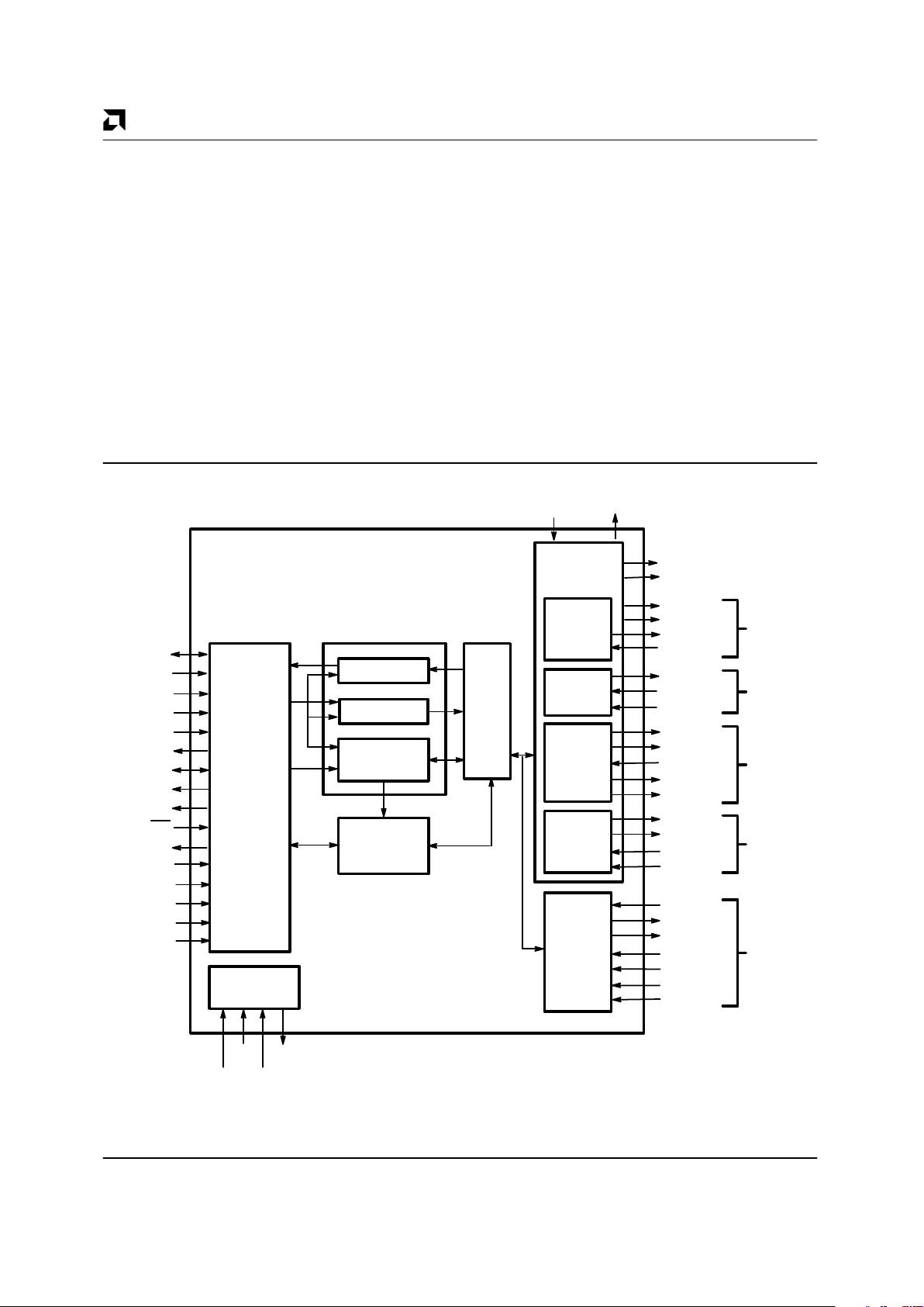
BLOCK DIAGRAM
DBUS 15-0
ADD 4-0
R/W
CS
FDS
DTV
EOF
RDTREQ
TDTREQ
BE 1–0
INTR
SCLK
EDSEL
TC
SLEEP
RESET
16235C-1
XTAL1
FIFO
Control
EADI Port
Bus
Interface
Unit
802.3
MAC
Core
ENCODER/
DECODER
(PLS)
XMT FIFO
RCV FIFO
Command
& Status
Registers
JTAG
PORT CNTRL
TCK
TDI
TMS
TDO
XTAL2
EADI
Port
Control
AUI
Port
10BASE-T
MAU
DAI
Port
GPSI
Port
DXCVR
CLSN
SRDCLK
SRD
SF/BD
EAM/R
DO±
DI±
CI±
TXD±
TXP±
RXD±
LNKST
RXPOL
TXDAT±
TXEN
RXDAT
RXCRS
STDCLK
TXDAT+
TXEN
SRDCLK
RXDAT
RXCRS
CLSN
AUI
10BASE-T
DAI Port
GPSI
Notes:
1. Only one of the network ports AUI, 10BASE-T, DAI port or GPSI can be active at any time. Some shared signals are active
regardless of which network port is active, and some are reconfigured.
2. The EADI port is active at all times.
Page 3

AMD
3Am79C940
RELATED PRODUCTS
Part No. Description
Am7996 IEEE 802.3/Ethernet/Cheapernet Transceiver
Am79C90 CMOS Local Area Network Controller for Ethernet (C-LANCE)
Am79C98 Twisted Pair Ethernet Transceiver (TPEX)
Am79C100 Twisted Pair Ethernet Transceiver Plus (TPEX+)
Am79C981 Integrated Multiport Repeater Plus (IMR+)
Am79C987 Hardware Implemented Management Information Base (HIMIB)
Am79C900 Integrated Local Area Communications Controller (ILACC)
Am79C961 PCnet-ISA
+
Single-Chip Ethernet Controller for ISA (with Microsoft Plug n’ Play Support)
Am79C965 PCnet-32 Single-Chip 32-Bit Ethernet Controller
Am79C970 PCnet-PCI Single-Chip Ethernet Controller (for PCI bus)
Am79C974 PCnet-SCSI Combination Ethernet and SCSI Controller for PCI Systems
Page 4

AMD
4 Am79C940
TABLE OF CONTENTS
DISTINCTIVE CHARACTERISTICS 1-64. . . . . . . . . . . . . . . . . . . . . . . . . . . . . . . . . . . . . . . . . . . .
GENERAL DESCRIPTION 1-64. . . . . . . . . . . . . . . . . . . . . . . . . . . . . . . . . . . . . . . . . . . . . . . . . . .
BLOCK DIAGRAM 1-65. . . . . . . . . . . . . . . . . . . . . . . . . . . . . . . . . . . . . . . . . . . . . . . . . . . . . . . . .
RELATED PRODUCTS 1-66. . . . . . . . . . . . . . . . . . . . . . . . . . . . . . . . . . . . . . . . . . . . . . . . . . . . . .
CONNECTION DIAGRAMS 1-70. . . . . . . . . . . . . . . . . . . . . . . . . . . . . . . . . . . . . . . . . . . . . . . . . .
PLCC 1-70. . . . . . . . . . . . . . . . . . . . . . . . . . . . . . . . . . . . . . . . . . . . . . . . . . . . . . . . . . . . . . . .
PQR 1-71. . . . . . . . . . . . . . . . . . . . . . . . . . . . . . . . . . . . . . . . . . . . . . . . . . . . . . . . . . . . . . . . .
PQT 1-72. . . . . . . . . . . . . . . . . . . . . . . . . . . . . . . . . . . . . . . . . . . . . . . . . . . . . . . . . . . . . . . . .
ORDERING 1-73. . . . . . . . . . . . . . . . . . . . . . . . . . . . . . . . . . . . . . . . . . . . . . . . . . . . . . . . . . . . . . .
PIN/PACKAGE SUMMARY 1-74. . . . . . . . . . . . . . . . . . . . . . . . . . . . . . . . . . . . . . . . . . . . . . . . . .
PIN DESCRIPTION 1-82. . . . . . . . . . . . . . . . . . . . . . . . . . . . . . . . . . . . . . . . . . . . . . . . . . . . . . . . .
Network Interfaces 1-82. . . . . . . . . . . . . . . . . . . . . . . . . . . . . . . . . . . . . . . . . . . . . . . . . . . . . . . . . .
Attachment Unit Interface (AUI) 1-82. . . . . . . . . . . . . . . . . . . . . . . . . . . . . . . . . . . . . . . . . . . .
Digital Attachment Interface (DAI) 1-82. . . . . . . . . . . . . . . . . . . . . . . . . . . . . . . . . . . . . . . . .
10BASE-T Interface 1-85. . . . . . . . . . . . . . . . . . . . . . . . . . . . . . . . . . . . . . . . . . . . . . . . . . . . .
General Purpose Serial Interface (GPSI) 1-85. . . . . . . . . . . . . . . . . . . . . . . . . . . . . . . . . . . . .
External Address Detection Interface (EADI) 1-86. . . . . . . . . . . . . . . . . . . . . . . . . . . . . . . .
Host System Interface 1-88. . . . . . . . . . . . . . . . . . . . . . . . . . . . . . . . . . . . . . . . . . . . . . . . . . .
IEEE 1149.1 Test Access Port (TAP) Interface 1-89. . . . . . . . . . . . . . . . . . . . . . . . . . . . . . . .
General Interface 1-89. . . . . . . . . . . . . . . . . . . . . . . . . . . . . . . . . . . . . . . . . . . . . . . . . . . . . . .
Power Supply 1-90. . . . . . . . . . . . . . . . . . . . . . . . . . . . . . . . . . . . . . . . . . . . . . . . . . . . . . . . . .
FUNCTIONAL DESCRIPTION 1-92. . . . . . . . . . . . . . . . . . . . . . . . . . . . . . . . . . . . . . . . . . . . . . . .
Network Interfaces 1-92. . . . . . . . . . . . . . . . . . . . . . . . . . . . . . . . . . . . . . . . . . . . . . . . . . . . . .
System Interface 1-92. . . . . . . . . . . . . . . . . . . . . . . . . . . . . . . . . . . . . . . . . . . . . . . . . . . . . . .
DETAILED FUNCTIONS 1-93. . . . . . . . . . . . . . . . . . . . . . . . . . . . . . . . . . . . . . . . . . . . . . . . . . . . .
Block Level Description 1-93. . . . . . . . . . . . . . . . . . . . . . . . . . . . . . . . . . . . . . . . . . . . . . . . . .
Bus Interface Unit (BIU) 1-93. . . . . . . . . . . . . . . . . . . . . . . . . . . . . . . . . . . . . . . . . . . . . .
BIU to FIFO Data Path 1-93. . . . . . . . . . . . . . . . . . . . . . . . . . . . . . . . . . . . . . . . . . .
BIU to Control and Status Register Data Path 1-94. . . . . . . . . . . . . . . . . . . . . . . . .
FIFO Sub-System 1-94. . . . . . . . . . . . . . . . . . . . . . . . . . . . . . . . . . . . . . . . . . . . . . . . . . .
Media Access Control (MAC) 1-96. . . . . . . . . . . . . . . . . . . . . . . . . . . . . . . . . . . . . . . . . .
Manchester Encoder/Decoder (MENDEC) 1-100. . . . . . . . . . . . . . . . . . . . . . . . . . . . . . .
Attachment Unit Interface (AUI) 1-103. . . . . . . . . . . . . . . . . . . . . . . . . . . . . . . . . . .
Digital Attachment Interface (DAI) 1-103. . . . . . . . . . . . . . . . . . . . . . . . . . . . . . . . .
10BASE-T Interface 1-104. . . . . . . . . . . . . . . . . . . . . . . . . . . . . . . . . . . . . . . . . . . . . . . .
Twisted Pair Transmit Function 1-104. . . . . . . . . . . . . . . . . . . . . . . . . . . . . . . . . . .
Twisted Pair Receive Function 1-104. . . . . . . . . . . . . . . . . . . . . . . . . . . . . . . . . . . .
Link Test Function 1-105. . . . . . . . . . . . . . . . . . . . . . . . . . . . . . . . . . . . . . . . . . . . . .
Polarity Detection and Reversal 1-105. . . . . . . . . . . . . . . . . . . . . . . . . . . . . . . . . . .
Twisted Pair Interface Status 1-106. . . . . . . . . . . . . . . . . . . . . . . . . . . . . . . . . . . . .
Collision Detect Function 1-106. . . . . . . . . . . . . . . . . . . . . . . . . . . . . . . . . . . . . . . .
Signal Quality Error (SQE) Test (Heartbeat) Function 1-106. . . . . . . . . . . . . . . . . .
Jabber Function 1-106. . . . . . . . . . . . . . . . . . . . . . . . . . . . . . . . . . . . . . . . . . . . . . .
Page 5

AMD
5Am79C940
External Address Detection Interface (EADI) 1-107. . . . . . . . . . . . . . . . . . . . . . . . . . . . .
General Purpose Serial Interface (GPSI) 1-108. . . . . . . . . . . . . . . . . . . . . . . . . . . . . . . .
IEEE 1149.1 Test Access Port Interface 1-108. . . . . . . . . . . . . . . . . . . . . . . . . . . . . . . .
Slave Access Operation 1-109. . . . . . . . . . . . . . . . . . . . . . . . . . . . . . . . . . . . . . . . . . . . . . . . .
Read Access 1-109. . . . . . . . . . . . . . . . . . . . . . . . . . . . . . . . . . . . . . . . . . . . . . . . . . . . . .
Write Access 1-110. . . . . . . . . . . . . . . . . . . . . . . . . . . . . . . . . . . . . . . . . . . . . . . . . . . . . .
Initialization 1-110. . . . . . . . . . . . . . . . . . . . . . . . . . . . . . . . . . . . . . . . . . . . . . . . . . . . . . .
Reinitialization 1-110. . . . . . . . . . . . . . . . . . . . . . . . . . . . . . . . . . . . . . . . . . . . . . . . . . . .
Transmit Operation 1-110. . . . . . . . . . . . . . . . . . . . . . . . . . . . . . . . . . . . . . . . . . . . . . . . . . . . .
Transmit FIFO Write 1-111. . . . . . . . . . . . . . . . . . . . . . . . . . . . . . . . . . . . . . . . . . . . . . . .
Transmit Function Programming 1-111. . . . . . . . . . . . . . . . . . . . . . . . . . . . . . . . . . . . . .
Automatic Pad Generation 1-112. . . . . . . . . . . . . . . . . . . . . . . . . . . . . . . . . . . . . . . . . . .
Transmit FCS Generation 1-113. . . . . . . . . . . . . . . . . . . . . . . . . . . . . . . . . . . . . . . . . . . .
Transmit Status Information 1-113. . . . . . . . . . . . . . . . . . . . . . . . . . . . . . . . . . . . . . . . . .
Transmit Exception Conditions 1-113. . . . . . . . . . . . . . . . . . . . . . . . . . . . . . . . . . . . . . . .
Receive Operation 1-115. . . . . . . . . . . . . . . . . . . . . . . . . . . . . . . . . . . . . . . . . . . . . . . . . . . . .
Receive FIFO Read 1-115. . . . . . . . . . . . . . . . . . . . . . . . . . . . . . . . . . . . . . . . . . . . . . . .
Receive Function Programming 1-116. . . . . . . . . . . . . . . . . . . . . . . . . . . . . . . . . . . . . . .
Automatic Pad Stripping 1-116. . . . . . . . . . . . . . . . . . . . . . . . . . . . . . . . . . . . . . . . . . . . .
Receive FCS Checking 1-117. . . . . . . . . . . . . . . . . . . . . . . . . . . . . . . . . . . . . . . . . . . . . .
Receive Status Information 1-117. . . . . . . . . . . . . . . . . . . . . . . . . . . . . . . . . . . . . . . . . . .
Receive Exception Conditions 1-117. . . . . . . . . . . . . . . . . . . . . . . . . . . . . . . . . . . . . . . .
Loopback Operation 1-118. . . . . . . . . . . . . . . . . . . . . . . . . . . . . . . . . . . . . . . . . . . . . . . . . . . .
USER ACCESSIBLE REGISTERS 1-120. . . . . . . . . . . . . . . . . . . . . . . . . . . . . . . . . . . . . . . . . . . .
Receive FIFO (RCVFIFO) 1-120. . . . . . . . . . . . . . . . . . . . . . . . . . . . . . . . . . . . . . . . . . . . . . .
Transmit FIFO (XMTFIFO) 1-120. . . . . . . . . . . . . . . . . . . . . . . . . . . . . . . . . . . . . . . . . . . . . . .
Transmit Frame Control (XMTFC) 1-120. . . . . . . . . . . . . . . . . . . . . . . . . . . . . . . . . . . . . . . . .
Transmit Frame Status (XMTFS) 1-121. . . . . . . . . . . . . . . . . . . . . . . . . . . . . . . . . . . . . . . . . .
Transmit Retry Count (XMTRC) 1-122. . . . . . . . . . . . . . . . . . . . . . . . . . . . . . . . . . . . . . . . . . .
Receive Frame Control (RCVFC) 1-122. . . . . . . . . . . . . . . . . . . . . . . . . . . . . . . . . . . . . . . . . .
Receive Frame Status (RCVFS) 1-123. . . . . . . . . . . . . . . . . . . . . . . . . . . . . . . . . . . . . . . . . .
RFS0—Receive Message Byte Count (RCVCNT) 1-123. . . . . . . . . . . . . . . . . . . . . . . . .
RFS1—Receive Status (RCVSTS) 1-123. . . . . . . . . . . . . . . . . . . . . . . . . . . . . . . . . . . . .
RFS2—Runt Packet Count (RNTPC) 1-124. . . . . . . . . . . . . . . . . . . . . . . . . . . . . . . . . . .
RFS3—Receive Collision Count (RCVCC) 1-124. . . . . . . . . . . . . . . . . . . . . . . . . . . . . . .
FIFO Frame Count (FIFOFC) 1-124. . . . . . . . . . . . . . . . . . . . . . . . . . . . . . . . . . . . . . . . . . . . .
Interrupt Register (IR) 1-124. . . . . . . . . . . . . . . . . . . . . . . . . . . . . . . . . . . . . . . . . . . . . . . . . . .
Interrupt Mask Register (IMR) 1-126. . . . . . . . . . . . . . . . . . . . . . . . . . . . . . . . . . . . . . . . . . . .
Poll Register (PR) 1-126. . . . . . . . . . . . . . . . . . . . . . . . . . . . . . . . . . . . . . . . . . . . . . . . . . . . . .
BIU Configuration Control (BIUCC) 1-127. . . . . . . . . . . . . . . . . . . . . . . . . . . . . . . . . . . . . . . .
FIFO Configuration Control (FIFOCC) 1-127. . . . . . . . . . . . . . . . . . . . . . . . . . . . . . . . . . . . . .
MAC Configuration Control (MACCC) 1-129. . . . . . . . . . . . . . . . . . . . . . . . . . . . . . . . . . . . . .
PLS Configuration Control (PLSCC) 1-130. . . . . . . . . . . . . . . . . . . . . . . . . . . . . . . . . . . . . . .
PHY Configuration Control (PHYCC) 1-130. . . . . . . . . . . . . . . . . . . . . . . . . . . . . . . . . . . . . . .
Chip Identification Register (CHIPID [15–00]) 1-131. . . . . . . . . . . . . . . . . . . . . . . . . . . . . . . .
Internal Address Configuration (IAC) 1-131. . . . . . . . . . . . . . . . . . . . . . . . . . . . . . . . . . . . . . .
Logical Address Filter (LADRF [63–00]) 1-132. . . . . . . . . . . . . . . . . . . . . . . . . . . . . . . . . . . . .
Page 6

AMD
6 Am79C940
Physical Address (PADR [47–00]) 1-134. . . . . . . . . . . . . . . . . . . . . . . . . . . . . . . . . . . . . . . . .
Missed Packet Count (MPC) 1-134. . . . . . . . . . . . . . . . . . . . . . . . . . . . . . . . . . . . . . . . . . . . .
Runt Packet Count (RNTPC) 1-134. . . . . . . . . . . . . . . . . . . . . . . . . . . . . . . . . . . . . . . . . . . . .
Receive Collision Count (RCVCC) 1-135. . . . . . . . . . . . . . . . . . . . . . . . . . . . . . . . . . . . . . . . .
User Test Register (UTR) 1-135. . . . . . . . . . . . . . . . . . . . . . . . . . . . . . . . . . . . . . . . . . . . . . . .
Reserved Test Register 1 (RTR1) 1-136. . . . . . . . . . . . . . . . . . . . . . . . . . . . . . . . . . . . . . . . .
Reserved Test Register 2 (RTR2) 1-136. . . . . . . . . . . . . . . . . . . . . . . . . . . . . . . . . . . . . . . . .
Register Table Summary 1-137. . . . . . . . . . . . . . . . . . . . . . . . . . . . . . . . . . . . . . . . . . . . . . . .
Register Bit Summary 1-138. . . . . . . . . . . . . . . . . . . . . . . . . . . . . . . . . . . . . . . . . . . . . . . . . .
16-Bit Registers 1-138. . . . . . . . . . . . . . . . . . . . . . . . . . . . . . . . . . . . . . . . . . . . . . . . . . .
8-Bit Registers 1-138. . . . . . . . . . . . . . . . . . . . . . . . . . . . . . . . . . . . . . . . . . . . . . . . . . . .
Receive Frame Status 1-138. . . . . . . . . . . . . . . . . . . . . . . . . . . . . . . . . . . . . . . . . . . . . .
Programmer’s Register Model 1-139. . . . . . . . . . . . . . . . . . . . . . . . . . . . . . . . . . . . . . . . . . . .
SYSTEM APPLICATIONS 1-142. . . . . . . . . . . . . . . . . . . . . . . . . . . . . . . . . . . . . . . . . . . . . . . . . . .
HOST SYSTEM EXAMPLES 1-142. . . . . . . . . . . . . . . . . . . . . . . . . . . . . . . . . . . . . . . . . . . . .
Motherboard DMA Controller 1-142. . . . . . . . . . . . . . . . . . . . . . . . . . . . . . . . . . . . . . . . .
System Interface-Motherboard DMA Example 1-143. . . . . . . . . . . . . . . . . . . . . . . .
PC/AT Ethernet Adapter Card 1-144. . . . . . . . . . . . . . . . . . . . . . . . . . . . . . . . . . . . . . . .
System Interface-Simple PC/AT Ethernet Hypercard Example 1-145. . . . . . . . . . .
NETWORK INTERFACES 1-145. . . . . . . . . . . . . . . . . . . . . . . . . . . . . . . . . . . . . . . . . . . . . . .
External Address Detection Interface (EADI) 1-145. . . . . . . . . . . . . . . . . . . . . . . . . . . . .
Attachment Unit Interface (AUI) 1-146. . . . . . . . . . . . . . . . . . . . . . . . . . . . . . . . . . . . . . .
10BASE-T Interface 1-147. . . . . . . . . . . . . . . . . . . . . . . . . . . . . . . . . . . . . . . . . . . . . . . .
10BASE-T and 10BASE2 Configuration of Am79C940 1-148. . . . . . . . . . . . . . . . . . . . .
10BASE-T and AUI Implementation of Am79C940 1-149. . . . . . . . . . . . . . . . . . . . . . . .
MACE Device Compatible AUI Isolation Transformers 1-150. . . . . . . . . . . . . . . . . . . . .
MACE Device Compatible 10BASE-T Media Interface Modules 1-150. . . . . . . . . . . . . .
ABSOLUTE MAXIMUM RATINGS 1-152. . . . . . . . . . . . . . . . . . . . . . . . . . . . . . . . . . . . . . . . . . . .
OPERATING RANGES 1-152. . . . . . . . . . . . . . . . . . . . . . . . . . . . . . . . . . . . . . . . . . . . . . . . . . . . .
DC CHARACTERISTICS 1-152. . . . . . . . . . . . . . . . . . . . . . . . . . . . . . . . . . . . . . . . . . . . . . . . . . . .
AC CHARACTERISTICS 1-155. . . . . . . . . . . . . . . . . . . . . . . . . . . . . . . . . . . . . . . . . . . . . . . . . . . .
BIU Output Valid Delay vs. Load Chart 1-159. . . . . . . . . . . . . . . . . . . . . . . . . . . . . . . . . . . . .
KEY TO SWITCHING WAVEFORMS 1-159. . . . . . . . . . . . . . . . . . . . . . . . . . . . . . . . . . . . . . . . . .
SWITCHING TEST CIRCUITS 1-160. . . . . . . . . . . . . . . . . . . . . . . . . . . . . . . . . . . . . . . . . . . . . . .
AC WAVEFORMS 1-161. . . . . . . . . . . . . . . . . . . . . . . . . . . . . . . . . . . . . . . . . . . . . . . . . . . . . . . . .
APPENDIX A 1-179. . . . . . . . . . . . . . . . . . . . . . . . . . . . . . . . . . . . . . . . . . . . . . . . . . . . . . . . . . . .
LOGICAL ADDRESS FILTERING FOR ETHERNET 1-179. . . . . . . . . . . . . . . . . . . . . . . . . .
MAPPING OF LOGICAL ADDRESS TO FILTER MASK 1-180. . . . . . . . . . . . . . . . . . . . . . .
APPENDIX B 1-181. . . . . . . . . . . . . . . . . . . . . . . . . . . . . . . . . . . . . . . . . . . . . . . . . . . . . . . . . . . .
BSDL DESCRIPTION OF Am79C940 MACE JTAG STRUCTURE 1-181. . . . . . . . . . . . . . .
Page 7
AMD
7Am79C940
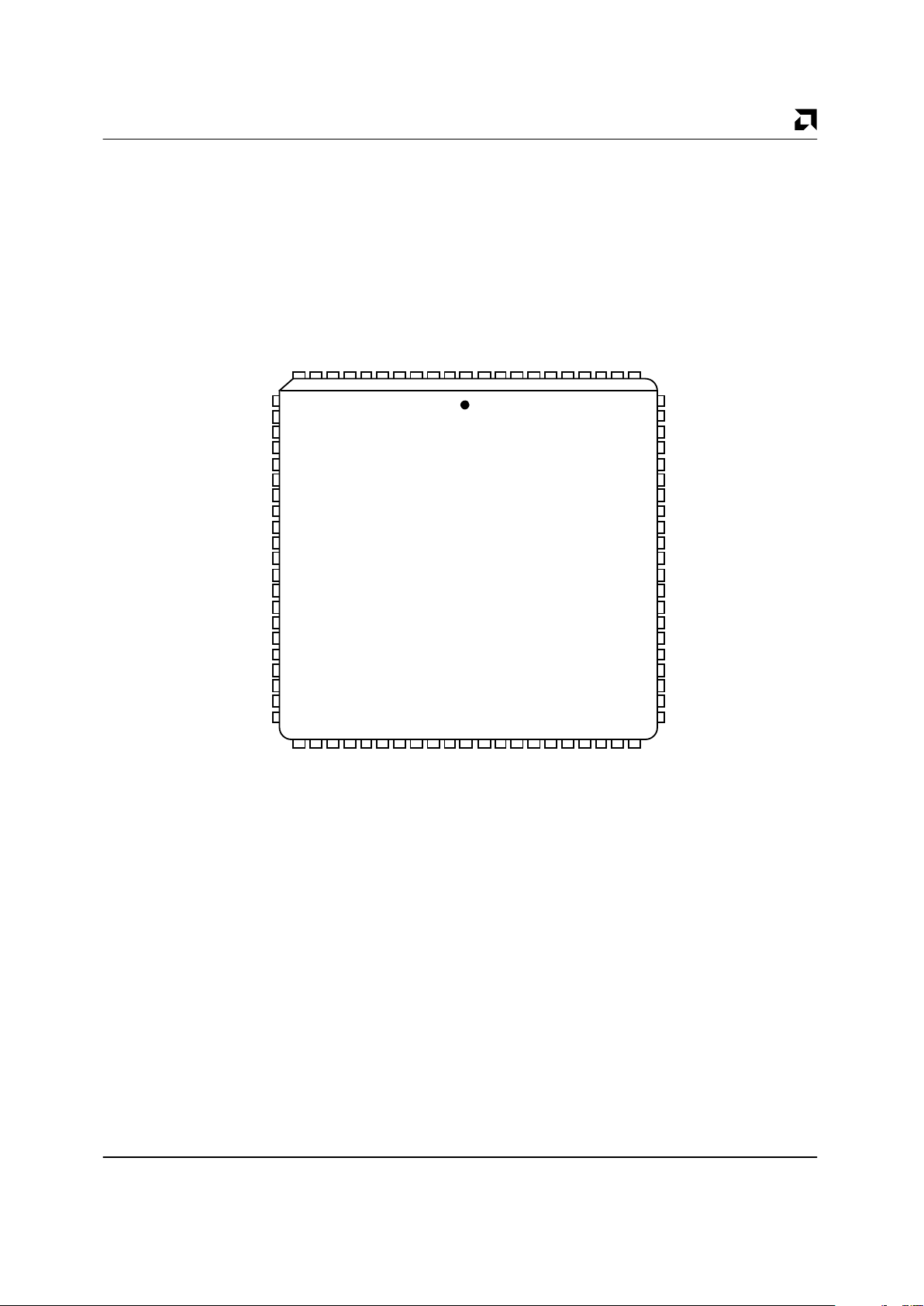
CONNECTION DIAGRAMS
PL 084
PLCC Package
16235C-2
1
2
3
81
82
83
84
6
7
8
9
4
5
80
76
77
78
79
75
12
13
14
15
16
17
18
19
20
21
23
24
25
26
27
28
29
30
31
73
72
71
70
69
68
67
66
65
64
63
62
61
60
59
58
57
56
55
54
43
42
41
40
47
46
45
44
37
36
35
34
39
38
33
48
52
51
50
49
10
22
11
32
53
74
SRDCLK
EAM/R
SRD
SF/BD
RESET
SLEEP
DV
DD
INTR
TC
DBUS0
DV
SS
DBUS1
DBUS2
DBUS3
DBUS4
DV
SS
DBUS5
DBUS6
DBUS7
DBUS8
DBUS9
XTAL2
AV
SS
XTAL1
AV
DD
TXD+
TXP+
TXD-
TXP-
AV
DD
RXD+
RXD-
DV
DD
TDI
DV
SS
TCK
TMS
TDO
LNKST
RXPOL
CS
R/W
RXCRS
RXDAT
CLSN
TXEN/TXEN
STDCLK
DV
SS
TXDAT-
TXDAT+
DV
SS
EDSEL
DXCVR
DV
DD
AV
DD
CI+
CI-
DI+
DI-
AV
DD
DO+
DO-
AV
SS
DBUS10
DBUS11
DBUS12
DBUS13
DV
DD
DBUS14
DBUS15
DV
SS
EOF
DTV
FDS
BE0
BE1
SCLK
TDTREQ
RDTREQ
ADD0
ADD1
ADD2
ADD3
ADD4
Am79C940
MACE
MACE
Am79C940JC
Page 8
AMD
8 Am79C940
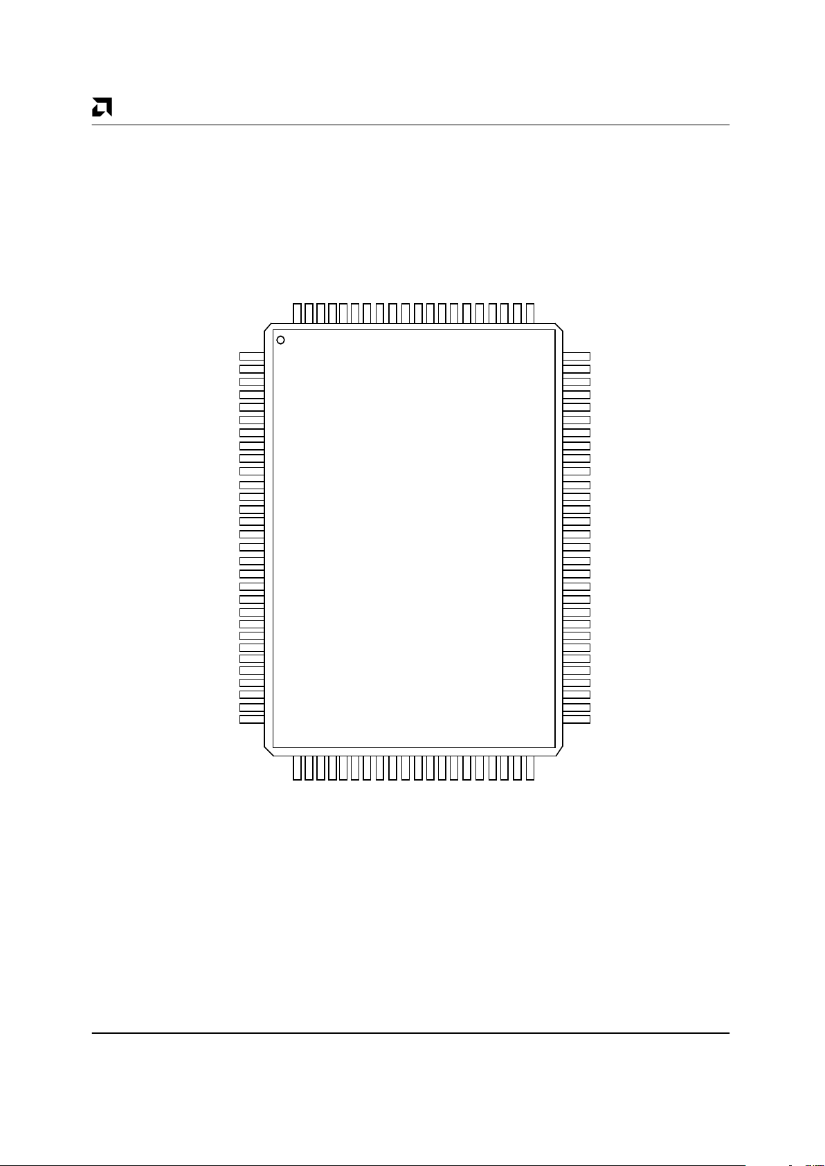
CONNECTION DIAGRAMS
PQR 100
PQFP Package
RXCRS
RXDAT
CLSN
TXEN/TXEN
STDCLK
DVSSTXDAT-
TXDAT+
DVSSEDSEL
DXCVR
DVDDAVDDCI+
CI-
DI+
DI-
AVDDDO+
DO-
28
29
30
4
5
6
7
8
9
10
11
12
13
14
15
16
17
18
19
20
21
22
23
24
25
26
27
1
2
3
99
98
100
31323334353637383940414243444546474849
50
9796959493929190898887868584828183
TCK
TMS
TDO
LNKST
RXPOL
CS
R/W
NC
NC
NC
NC
AV
SS
NC
NC
NC
XTAL2
AV
SS
XTAL1
AV
DD
TXD+
TXP+
TXDTXPAV
DD
RXD+
RXDDV
DD
TDI
DV
SS
NC
77
76
75
74
73
72
71
70
69
68
67
66
65
64
63
62
61
60
59
58
57
56
55
54
53
52
51
80
79
78
NC
NC
NC
NC
SRDCLK
EAM/R
SRD
SF/BD
RESET
SLEEP
DV
DD
INTR
TC
DBUS0
DV
SS
DBUS1
DBUS2
DBUS3
DBUS4
DV
SS
DBUS5
DBUS6
DBUS7
DBUS8
DBUS9
NC
NC
NC
DBUS10
NC
DBUS11
DBUS12
DBUS13
DV
DD
DBUS14
DBUS15
DV
SS
EOF
DTV
FDS
BE0
BE1
SCLK
TDTREQ
RDTREQ
ADD0
ADD1
ADD2
ADD3
ADD4
MACE
Am79C940KC
16235C-3
MACE
Am79C940KC
Page 9
AMD
9Am79C940
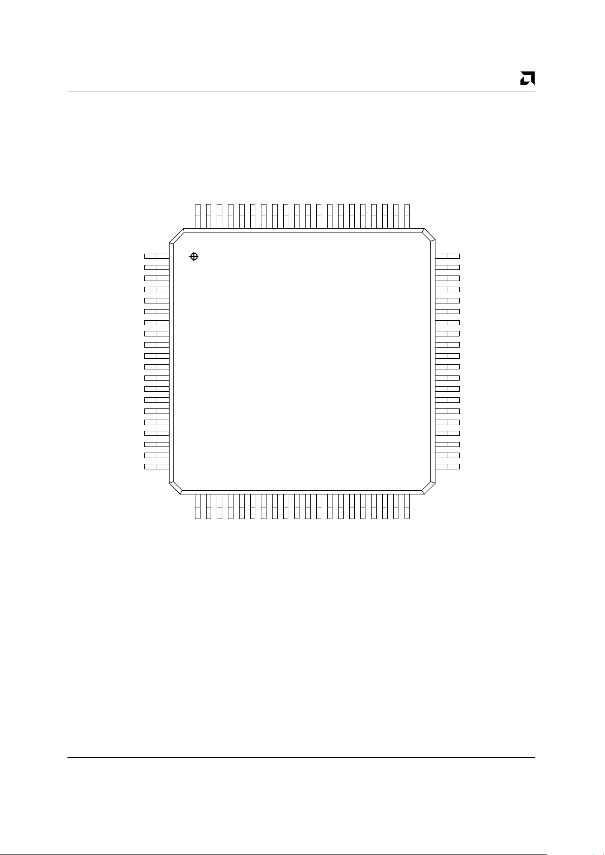
CONNECTION DIAGRAMS
PQT 080
TQFP Package
16235C-4
Note: Four pin functions available on the PLCC and PQFP packages are not available with the TQFP package.
(See page 27 “Pin Functions not available with the 80-pin TQFP Package”).
1
2
3
4
5
6
7
8
9
10
11
12
13
14
15
16
17
18
19
20
60
59
58
57
56
55
54
53
52
51
50
49
48
47
46
45
44
43
42
41
80 79 78 77 76 757473 72 71 7069 68 676665 64 63 62 61
21 22 23 24 25 262728 29 30 3132 33 343536 37 38 39 40
SRDCLK
EAM/R
SF/BD
RESET
SLEEP
DVDD
INTR
TC
DBUS0
DVSS
DBUS1
DBUS2
DBUS3
DBUS4
DVSS
DBUS5
DBUS6
DBUS7
DBUS8
DBUS9
XTAL2
AVSS
XTAL1
AVDD
TXD+
TXP+
TXDTXPAVDD
RXD+
RXDDVDD
TDI
DVSS
TCK
TMS
TD0
LNKST
CS
R/W
DBUS10
DBUS11
DBUS12
DBUS13
DVDD
DBUS14
DBUS15
DVSS
EOF
FDS
BE0
BE1
SCLK
TDTREQ
RDTREQ
ADD0
ADD1
ADD2
ADD3
ADD4
RXCRS
RXDAT
CLSN
TXEN/TXEN
STDCLK
DVSS
TXDAT+
DVSS
EDSEL
DXCVR
DVDD
AVDD
CI+
CI-
DI+
DI-
AVDD
DO+
DO-
AVSS
MACE
Am79C940VC
Page 10

AMD
10 Am79C940
ORDERING INFORMATION
Standard Products
AMD standard products are available in several packages and operating ranges. The order number (Valid Combination) is
formed by a combination of:
AM79C940
JC, KC,
Valid Combinations
Valid Combinations
The Valid Combinations table lists configurations
planned to be supported in volume for this device.
Consult the local AMD sales office to confirm
availability of specific valid combinations and to
check on newly released combinations.
AM79C940
OPTIONAL PROCESSING
Blank = Standard Processing
TEMPERATURE RANGE
C = Commercial (0
° to +70°C)
PACKAGE TYPE (per Prod. Nomenclature/16-038)
J = 84-Pin Plastic Leaded Chip Carrier (PL 084)
K = 100-Pin Plastic Quad Flat Pack (PQR100)
V = 80-Pin Thin Quad Flat Package (PQT080)
SPEED
Not Applicable
DEVICE NUMBER/DESCRIPTION (include revision letter)
Am79C940
Media Access Controller for Ethernet
VC
ALTERNATE PACKAGING OPTION
/W = Trimmed and Formed in a Tray
KC/W, VC,
/W
VC/W
Page 11

AMD
11Am79C940
PIN/PACKAGE SUMMARY
PLCC Pin # Pin Name Pin Function
1 DXCVR Disable Transceiver
2 EDSEL Edge Select
3DV
SS
Digital Ground
4 TXDAT+ Transmit Data +
5 TXDAT– Transmit Data –
6DV
SS
Digital Ground
7 STDCLK Serial Transmit Data Clock
8 TXEN/TXEN Transmit Enable
9 CLSN Collision
10 RXDAT Receive Data
11 RXCRS Receive Carrier Sense
12 SRDCLK Serial Receive Data Clock
13 EAM/R External Address Match/Reject
14 SRD Serial Receive Data
15 SF/BD Start Frame/Byte Delimiter
16 RESET Reset
17 SLEEP Sleep Mode
18 DV
DD
Digital Power
19 INTR Interrupt
20 TC Timing Control
21 DBUS0 Data Bus0
22 DV
SS
Digital Ground
23 DBUS1 Data Bus1
24 DBUS2 Data Bus2
25 DBUS3 Data Bus3
26 DBUS4 Data Bus4
27 DV
SS
Digital Ground
28 DBUS5 Data Bus5
29 DBUS6 Data Bus6
30 DBUS7 Data Bus7
31 DBUS8 Data Bus8
32 DBUS9 Data Bus9
33 DBUS10 Data Bus10
34 DBUS11 Data Bus11
35 DBUS12 Data Bus12
36 DBUS13 Data Bus13
37 DV
DD
Digital Power
38 DBUS14 Data Bus14
39 DBUS15 Data Bus15
40 DV
SS
Digital Ground
41 EOF End Of Frame
42 DTV Data Transfer Valid
Page 12

AMD
12 Am79C940
PIN/PACKAGE SUMMARY (continued)
PLCC Pin # Pin Name Pin Function
43 FDS FIFO Data Strobe
44 BE0 Byte Enable0
45 BE1 Byte Enable1
46 SCLK System Clock
47 TDTREQ Transmit Data Transfer Request
48 RDTREQ Receive Data Transfer Request
49 ADD0 Address0
50 ADD1 Address1
51 ADD2 Address2
52 ADD3 Address3
53 ADD4 Address4
54 R/W Read/Write
55 CS Chip Select
56 RXPOL Receive Polarity
57 LNKST Link Status
58 TDO Test Data Out
59 TMS Test Mode Select
60 TCK Test Clock
61 DV
SS
Digital Ground
62 TDI Test Data Input
63 DV
DD
Digital Power
64 RXD– Receive Data–
65 RXD+ Receive Data+
66 AV
DD
Analog Power
67 TXP– Transmit Pre-distortion
68 TXD– Transmit Data–
69 TXP+ Transmit Pre–distortion+
70 TXD+ Transmit Data+
71 AV
DD
Analog Power
72 XTAL1 Crystal Input
73 AV
SS
Analog Ground
74 XTAL2 Crystal Output
75 AV
SS
Analog Ground
76 DO– Data Out–
77 DO+ Data Out+
78 AV
DD
Analog Power
79 DI– Data In–
80 DI+ Data In+
81 CI– Control In–
82 CI+ Control In+
83 AV
DD
Analog Power
84 DV
DD
Digital Power
Page 13

AMD
13Am79C940
PIN/PACKAGE SUMMARY (continued)
PQFP Pin # Pin Name Pin Function
1 NC No Connect
2 NC No Connect
3 NC No Connect
4 NC No Connect
5 SRDCLK Serial Receive Data Clock
6 EAM/R External Address Match/Reject
7 SRD Serial Receive Data
8 SF/BD Start Frame/Byte Delimiter
9 RESET Reset
10 SLEEP Sleep Mode
11 DVDD Digital Power
12 INTR Interrupt
13 TC Timing Control
14 DBUS0 Data Bus0
15 DV
SS
Digital Ground
16 DBUS1 Data Bus1
17 DBUS2 Data Bus2
18 DBUS3 Data Bus3
19 DBUS4 Data Bus4
20 DV
SS
Digital Ground
21 DBUS5 Data Bus5
22 DBUS6 Data Bus6
23 DBUS7 Data Bus7
24 DBUS8 Data Bus8
25 DBUS9 Data Bus9
26 NC No Connect
27 NC No Connect
28 NC No Connect
29 DBUS10 Data Bus10
30 NC No Connect
31 DBUS11 Data Bus11
32 DBUS12 Data Bus12
33 DBUS13 Data Bus13
34 DV
DD
Digital Power
35 DBUS14 Data Bus14
36 DBUS15 Data Bus15
37 DV
SS
Digital Ground
38 EOF End Of Frame
39 DTV Data Transfer Valid
40 FDS FIFO Data Strobe
41 BE0 Byte Enable0
42 BE1 Byte Enable1
Page 14

AMD
14 Am79C940
PIN/PACKAGE SUMMARY (continued)
PQFP Pin # Pin Name Pin Function
43 SCLK System Clock
44 TDTREQ Transmit Data Transfer Request
45 RDTREQ Receive Data Transfer Request
46 ADD0 Address0
47 ADD1 Address1
48 ADD2 Address2
49 ADD3 Address3
50 ADD4 Address4
51 NC No Connect
52 NC No Connect
53 NC No Connect
54 NC No Connect
55 R/W Read/Write
56 CS Chip Select
57 RXPOL Receive Polarity
58 LNKST Link Status
59 TDO Test Data Out
60 TMS Test Mode Select
61 TCK Test Clock
62 DV
SS
Digital Ground
63 TDI Test Data Input
64 DV
DD
Digital Power
65 RXD– Receive Data–
66 RXD+ Receive Data+
67 AV
DD
Analog Power
68 TXP– Transmit Pre-distortion–
69 TXD– Transmit Data–
70 TXP+ Transmit Pre-distortion+
71 TXD+ Transmit Data+
72 AV
DD
Analog Power
73 XTAL1 Crystal Input
74 AV
SS
Analog Ground
75 XTAL2 Crystal Output
76 NC No Connect
77 NC No Connect
78 NC No Connect
79 AV
SS
Analog Ground
80 NC No Connect
81 DO– Data Out–
82 DO+ Data Out+
83 AV
DD
Analog Power
84 DI– Data In–
85 DI+ Data In+
Page 15

AMD
15Am79C940
PIN/PACKAGE SUMMARY (continued)
PQFP Pin # Pin Name Pin Function
86 CI– Control In–
87 CI+ Control In+
88 AV
DD
Analog Power
89 DV
DD
Digital Power
90 DXCVR Disable Transceiver
91 EDSEL Edge Select
92 DV
SS
Digital Ground
93 TXDAT+ Transmit Data +
94 TXDAT– Transmit Data –
95 DV
SS
Digital Ground
96 STDCLK Serial Transmit Data Clock
97 TXEN/TXEN Transmit Enable
98 CLSN Collision
99 RXDAT Receive Data
100 RXCRS Receive Carrier Sense
Page 16

AMD
16 Am79C940
PIN/PACKAGE SUMMARY (continued)
TQFP TQFP
Pin Number Pin Name Pin Function Pin Number Pin Name Pin Function
1 SRDCLK Serial Receive Data Clock 41 R/W Read/Write
2 EAM/R External Address Match/Reject 42 CS Chip/Select
3 SF/BD Start Frame/Byte Delimiter 43 LNKST Link Status
4 RESET Reset 44 TDO Test Data Out
5 SLEEP Sleep Mode 45 TMS Test Mode Select
6 DVDD Digital Power 46 TCK Test Clock
7 INTR Interrupt 47 DVSS Digital Ground
8 TC Timing Control 48 TDI Test Data Input
9 DBUS0 Data Bus0 49 DVDD Digital Power
10 DVSS Digital Ground 50 RXD– Receive Data–
11 DBUS1 Data Bus1 51 RXD+ Receive Data+
12 DBUS2 Data Bus2 52 AVDD Analog Power
13 DBUS3 Data Bus3 53 TXP– Transmit Pre-distortion–
14 DBUS4 Data Bus4 54 TXD– Transmit Data–
15 DVSS Digital Ground 55 TXP+ Transmit Pre-distortion+
16 DBUS5 Data Bus5 56 TXD+ Transmit Data+
17 DBUS6 Data Bus6 57 AVDD Analog Power
18 DBUS7 Data Bus7 58 XTAL1 Crystal Output
19 DBUS8 Data Bus8 59 AVSS Analog Ground
20 DBUS9 Data Bus9 60 XTAL2 Crystal Output
21 DBUS10 Data Bus10 61 AVSS Analog Ground
22 DBUS11 Data Bus11 62 DO– Data Out–
23 DBUS12 Data Bus12 63 DO+ Data Out+
24 DBUS13 Data Bus13 64 AVDD Analog Power
25 DVDD Digital Power 65 DI– Data In–
26 DBUS14 Data Bus14 66 DI+ Data Out+
27 DBUS15 Data Bus15 67 CI– Control In–
28 DVSS Digital Ground 68 CI+ Control In+
29 EOF End of Frame 69 AVDD Analog Power
30 FDS FIFO Data Strobe 70 DVDD Digital Power
31 BE0 Byte Enable0 71 DXCVR Disable Transceiver
32 BE1 Byte Enable1 72 EDSEL Edge Select
33 SCLK System Clock 73 DVSS Digital Ground
34 TDTREQ Transmit Data Transfer Request 74 TXDAT+ Transmit Data+
35 RDTREQ Receive Data Transfer Request 75 DVSS Digital Ground
36 ADD0 Address0 76 STDCLK Serial Transmit Data Clock
37 ADD1 Address1 77 TXEN/TXEN Transmit Enable
38 ADD2 Address2 78 CLSN Collision
39 ADD3 Address3 79 RXDAT Receive Data
40 ADD4 Address4 80 RXCRS Receive Carrier Sense
Page 17

AMD
17Am79C940
PIN SUMMARY
Pin Name Pin Function Type Active Comment
Attachment Unit Interface (AUI)
DO+/DO– Data Out O Pseudo-ECL
DI+/DI– Data In I Pseudo-ECL
CI+/CI– Control In I Pseudo-ECL
RXCRS Receive Carrier Sense I/O High TTL output. Input in DAI, GPSI port
TXEN Transmit Enable O High TTL. TXEN in DAI port
CLSN Collision I/O High TTL output. Input in GPSI
DXCVR Disable Transceiver O Low TTL low
STDCLK Serial Transmit Data Clock I/O Output. Input in GPSI
SRDCLK Serial Receive Data Clock I/O Output. Input in GPSI
Digital Attachment Interface (DAI)
TXDAT+ Transmit Data + O High TTL. See also GPSI
TXDAT– Transmit Data – O Low TTL
TXEN Transmit Enable O Low TTL. See TXEN in GPSI
RXDAT Receive Data I TTL. See also GPSI
RXCRS Receive Carrier Sense I/O High TTL input. Output in AUI
CLSN Collision I/O High TTL output. Input in GPSI
DXCVR Disable Transceiver O High TTL high
STDCLK Serial Transmit Data Clock I/O Output. Input in GPSI
SRDCLK Serial Receive Data Clock I/O Output. Input in GPSI
10BASE–T Interface
TXD+/TXD– Transmit Data O
TXP+/TXP– Transmit Pre-distortion O
RXD+/RXD– Receive Data I
LNKST Link Status O Low Open Drain
RXPOL Receive Polarity O Low Open Drain
TXEN Transmit Enable O High TTL. TXEN in DAI port
RXCRS Receive Carrier Sense I/O High TTL output. Input in DAI, GPSI port
CLSN Collision I/O High TTL output. Input in GPSI
DXCVR Disable Transceiver O High TTL high
STDCLK Serial Transmit Data Clock I/O Output. Input in GPSI
SRDCLK Serial Receive Data Clock I/O Output. Input in GPSI
General Purpose Serial Interface (GPSI)
STDCLK Serial Transmit Data Clock I/O Input
TXDAT+ Transmit Data + O High TTL. See also DAI port
TXEN Transmit Enable O High TTL. TXEN in DAI port
SRDCLK Serial Receive Data Clock I/O Input. See also EADI port
RXDAT Receive Data I TTL. See also DAI port
RXCRS Receive Carrier Sense I/O High TTL input. Output in AUI
CLSN Collision I/O High TTL input
DXCVR Disable Transceiver O Low TTL low
Page 18

AMD
18 Am79C940
PIN SUMMARY (continued)
Pin Name Pin Function Type Active Comment
External Address Detection Interface (EADI)
SF/BD Start Frame/Byte Delimiter O High
SRD Serial Receive Data O High
EAM/R External Address Match/Reject I Low
SRDCLK Serial Receive Data Clock I/O Output except in GPSI
Host System Interface
DBUS15–0 Data Bus I/O High
ADD4–0 Address I High
R/W Read/Write I High/Low
RDTREQ Receive Data Transfer Request O Low
TDTREQ Transmit Data Transfer Request O Low
DTV Data Transfer Valid O Low Tristate
EOF End Of Frame I/O Low
BE0 Byte Enable 0 I Low
BE1 Byte Enable 1 I Low
CS Chip Select I Low
FDS FIFO Data Strobe I Low
INTR Interrupt O Low Open Drain
EDSEL Edge Select I High
TC Timing Control I Low Internal pull-up
SCLK System Clock I High
RESET Reset I Low
IEEE 1149.1 Test Access Port (TAP) Interface
TCK Test Clock I Internal pull-up
TMS Test Mode Select I Internal pull-up
TDI Test Data Input I Internal pull-up
TDO Test Data Out O
General Interface
XTAL1 Crystal Input I CMOS
XTAL2 Crystal Output O CMOS
SLEEP Sleep Mode I Low TTL
DV
DD
Digital Power (4 pins) P
DV
SS
Digital Ground (6 pins) P
AV
DD
Analog Power (4 pins) P
AV
SS
Analog Ground (2 pins) P
Page 19

AMD
19Am79C940
PIN DESCRIPTION
Network Interfaces
The MACE device has five potential network interfaces.
Only one of the interfaces that provides physical network attachment can be used (active) at any time. Selection between the AUI, 10BASE-T, DAI or GPSI ports
is provided by programming the PHY Configuration
Control register. The EADI port is effectively active at all
times. Some signals, primarily used for status reporting,
are active for more than one single interface (the CLSN
pin for instance). Under each of the descriptions for the
network interfaces, the primary signals which are
unique to that interface are described. Where signals
are active for multiple interfaces, they are described
once under the interface most appropriate.
Attachment Unit Interface (AUI)
CI+/CI
Control In
(Input)
A differential input pair, signalling the MACE device that
a collision has been detected on the network media, indicated by the CI± inputs being exercised with 10 MHz
pattern of sufficient amplitude and duration. Operates at
pseudo-ECL levels.
DI+/DI
Data In
(Input)
A differential input pair to the MACE device for receiving
Manchester encoded data from the network. Operates
at pseudo-ECL levels.
DO+/DO
Data Out
(Output)
A differential output pair from the MACE device for
transmitting Manchester encoded data to the network.
Operates at pseudo-ECL levels.
Digital Attachment Interface (DAI)
TXDAT+/TXDAT–
Transmit Data
(Output)
When the DAI port is selected, TXDAT± are configured
as a complementary pair for Manchester encoded data
output from the MACE device, used to transmit data to a
local external network transceiver. During valid transmission (indicated by TXEN low), a logical
1
is indicated
by the TXDAT+ pin being in the high state and TXDAT–
in the low state; and a logical
0
is indicated by the
TXDAT+ pin being in the low state and TXDAT– in the
high state. During idle (TXEN high), TXDAT+ will be in
the high state, and TXDAT– in the low state. When the
GPSI port is selected, TXDAT+ will provide NRZ data
output from the MAC core, and TXDAT– will be held in
the LOW state. Operates at TTL levels. The operations
of TXDAT+ and TXDAT– are defined in the following
tables:
TXDAT+ Configuration
PORTSEL
SLEEP [1–0] ENPLSIO Interface Description Pin Function
0 XX X Sleep Mode High Impedance
1 00 1 AUI High Impedance (Note 2)
1 01 1 10BASE-T High Impedance (Note 2)
1 10 1 DAI Port TXDAT+ Output
1 11 1 GPSI TXDAT+ Output
1 XX 0 Status Disabled High Impedance (Note 2)
TXDAT– Configuration
PORTSEL
SLEEP [1–0] ENPLSIO Interface Description Pin Function
0 XX X Sleep Mode High Impedance
1 00 1 AUI High Impedance
1 01 1 10BASE-T High Impedance
1 10 1 DAI Port TXDAT– Output
1 11 1 GPSI LOW
1 XX 0 Status Disabled High Impedance
Notes:
1. PORTSEL [1–0] and ENPLSIO are located in the PLS Configuration Control register (REG ADDR 14).
2. This pin should be externally terminated, if unused, to reduce power consumption.
Page 20

AMD
20 Am79C940
TXEN/TXEN
Transmit Enable
(Output)
When the AUI port is selected (PORTSEL [1–0] = 00),
an output indicating that the AUI DO± differential output
has valid Manchester encoded data is presented. When
the 10BASE-T port is selected (PORTSEL [1–0] = 01),
indicates that Manchester data is being output on the
TXD±/TXP± complementary outputs. When the DAI
port is selected (PORTSEL [1–0] = 10), indicates that
Manchester data is being output on the DAI port
TXDAT± complementary outputs. When the GPSI port
is selected (PORTSEL [1–0] =11), indicates that NRZ
data is being output from the MAC core of the MACE device, to an external Manchester encoder/decoder, on
the TXDAT+ output. Active low when the DAI port is selected, active high when the AUI, 10 BASE-T or GPSI is
selected. Operates at TTL levels.
RXDAT
Receive Data
(Input)
When the DAI port is selected (PORTSEL [1–0] = 10),
the Manchester encoded data input to the integrated
clock recovery and Manchester decoder of the MACE
device, from an external network transceiver. When the
GPSI port is selected (PORTSEL [1–0] =11), the NRZ
decoded data input to the MAC core of the MACE device, from an external Manchester encoder/decoder.
Operates at TTL levels.
RXCRS
Receive Carrier Sense
(Input/Output)
When the AUI port is selected (PORTSEL [1–0] = 00),
an output indicating that the DI± input pair is receiving
valid Manchester encoded data from the external transceiver which meets the signal amplitude and pulse width
requirements. When the 10BASE-T port is selected
(PORTSEL [1–0] = 01), an output indicating that the
RXD± input pair is receiving valid Manchester encoded
data from the twisted pair cable which meets the signal
amplitude and pulse width requirements. RXCRS will be
asserted high for the entire duration of the receive message. When the DAI port is selected (PORTSEL [1–0] =
10), an input signaling the MACE device that a receive
carrier condition has been detected on the network, and
valid Manchester encoded data is being presented to
the MACE device on the RXDAT line. When the GPSI
port is selected (PORTSEL [1–0] = 11), an input signalling the internal MAC core that valid NRZ data is being
presented on the RXDAT input. Operates at TTL levels.
TXEN/TXEN Configuration
PORTSEL
SLEEP [1–0] ENPLSIO Interface Description Pin Function
0 XX X Sleep Mode High Impedance
1 00 1 AUI TXEN Output
1 01 1 10BASE-T TXEN Output
1 10 1 DAI Port TXEN Output
1 11 1 GPSI TXEN Output
1 XX 0 Status Disabled High Impedance (Note 3)
Notes:
1. PORTSEL [1–0] and ENPLSIO are located in the PLS Configuration Control register (REG ADDR 14).
2. When the GPSI port is selected, TXEN should have an external pull-down attached (e.g. 3.3k
Ω
) to ensure the output is held
inactivebefore ENPLSIO is set.
3. This pin should be externally terminated, if unused, to reduce power consumption.
RXDAT Configuration
PORTSEL
SLEEP [1–0] ENPLSIO Interface Description Pin Function
0 XX X Sleep Mode High Impedance
1 00 1 AUI High Impedance (Note 2)
1 01 1 10BASE-T High Impedance (Note 2)
1 10 1 DAI Port RXDAT Input
1 11 1 GPSI RXDAT Input
1 XX 0 Status Disabled High Impedance (Note 2)
Notes:
1. PORTSEL [1–0] and ENPLSIO are located in the PLS Configuration Control register (REG ADDR 14).
2. This pin should be externally terminated, if unused, to reduce power consumption.
Page 21

AMD
21Am79C940
RXCRS Configuration
PORTSEL
SLEEP [1–0] ENPLSIO Interface Description Pin Function
0 XX X Sleep Mode High Impedance
1 00 1 AUI RXCRS Output
1 01 1 10BASE-T RXCRS Output
1 10 1 DAI Port RXCRS Input
1 11 1 GPSI RXCRS Input
1 XX 0 Status Disabled High Impedance (Note 2)
Notes:
1. PORTSEL [1–0] and ENPLSIO are located in the PLS Configuration Control register (REG ADDR 14).
2. This pin should be externally terminated, if unused, to reduce power consumption.
DXCVR
Disable Transceiver
(Output)
An output from the MACE device to indicate the network
port in use, as programmed by the ASEL bit or the
PORTSEL [1–0] bits. The output is provided to allow
power down of an external DC-to-DC converter, typically used to provide the voltage requirements for an external 10BASE2 transceiver.
When the Auto Select (ASEL) feature is enabled, the
state of the PORTSEL [1–0] bits is overridden, and the
network interface will be selected by the MACE device,
dependent only on the status of the 10BASE-T link. If the
link is active (LNKST pin driven LOW) the 10BASE-T
port will be used as the active network interface. If the
link is inactive (LNKST pin pulled HIGH) the AUI port will
be used as the active network interface. Auto Select will
continue to operate even when the SLEEP pin is asserted if the RWAKE bit has been set. The AWAKE bit
does not allow the Auto Select function, and only the receive section of 10BASE-T port will be active (DXCVR =
HIGH).
Active (HIGH) when either the 10BASE-T or DAI port is
selected. Inactive (LOW) when the AUI or GPSI port is
selected.
DXCVR Configuration—SLEEP Operation
SLEEP RWAKE AWAKE ASEL LNKST PORTSEL Interface Pin
Pin Bit Bit Bit Pin [1–0] Bits Description Function
0 0 0 X High XX Sleep High
Impedance Mode Impedance
0 1 0 0 High 00 AUI with EADI port LOW
Impedance
0 1 0 0 High 01 10BASE-T with EADI port HIGH
Impedance
0 1 0 0 High 10 Invalid HIGH
Impedance
0 1 0 0 High 11 Invalid LOW
Impedance
0 1 0 1 High 0X AUI with EADI port LOW
Impedance
0 1 0 1 High 0X 10BASE-T with EADI port HIGH
Impedance
0 1 1 1 HIGH 0X AUI with EADI port LOW
0 1 1 1 LOW 0X 10BASE-T with EADI port HIGH
0 0 1 X X 0X 10BASE-T HIGH
Note: RWAKE and ASEL are located in the PHY Configuration Control register (REG ADDR 15). PORTSEL [1–0] and
ENPLSIO are located in the PLS Configuration Control register (REG ADDR 14). All bits must be programmed prior to the
assertion of the
SLEEP
pin.
Page 22

AMD
22 Am79C940
DXCVR Configuration—Normal Operation
SLEEP ASEL LNKST PORTSEL ENPLSIO Interface Pin
Pin Bit Pin [1–0] Bits Bit Description Function
1 X X XX X SIA Test Mode High
Impedance
1 0 X 00 X AUI LOW
1 0 X 01 X 10BASE-T HIGH
1 0 X 10 X DAI Port HIGH
1 0 X 11 X GPSI LOW
1 1 HIGH 0X X AUI LOW
1 1 LOW 0X X 10BASE-T HIGH
Note: RWAKE and ASEL are located in the PHY Configuration Control register (REG ADDR 15). PORTSEL [1–0] and
ENPLSIO are located in the PLS Configuration Control register (REG ADDR 14).
10BASE-T Interface
TXD+, TXD–
Transmit Data
(Output)
10BASE-T port differential drivers.
TXP+, TXP–
Transmit Pre-Distortion
(Output)
Transmit wave form differential driver for pre-distortion.
RXD+, RXD–
Receive Data
(Input)
10BASE-T port differential receiver. These pins should
be externally terminated to reduce power consumption if
the 10BASE-T interface is not used.
LNKST
Link Status
(OutputOpen Drain)
This pin is driven LOW if the link is identified as functional. If the link is determined to be nonfunctional, due
to missing idle link pulses or data packets, then this pin
is not driven (requires external pull-up). In the LOW output state, the pin is capable of sinking a maximum of
12 mA and can be used to drive an LED.
This feature can be disabled by setting the Disable Link
Test (DLNKTST) bit in the PHY Configuration Control
register. In this case the internal Link Test Receive function is disabled, the LNKST pin will be driven LOW, and
the Transmit and Receive functions will remain active
regardless of arriving idle link pulses and data. The internal 10BASE-T MAU will continue to generate idle link
pulses irrespective of the status of the DLNKTST bit.
RXPOL
Receive Polarity
(Output, Open Drain)
The twisted pair receiver is capable of detecting a receive signal with reversed polarity (wiring error). The
RXPOL pin is normally in the LOW state, indicating correct polarity of the received signal. If the receiver detects
a received packet with reversed polarity, then this pin is
not driven (requires external pull–up) and the polarity of
subsequent packets are inverted. In the LOW output
state, this pin is capable of sinking a maximum of 12mA
and can be used to drive an LED.
The polarity correction feature can be disabled by setting the Disable Auto Polarity Correction (DAPC) bit in
the PHY Configuration Control register. In this case, the
Receive Polarity correction circuit is disabled and the internal receive signal remains non-inverted, irrespective
of the received signal. Note that RXPOL will continue to
reflect the polarity detected by the receiver.
General Purpose Serial Interface (GPSI)
STDCLK
Serial Transmit Data Clock
(Input/Output)
When either the AUI, 10BASE-T or DAI port is selected,
STDCLK is an output operating at one half the crystal or
XTAL1 frequency. STDCLK is the encoding clock for
Manchester data transferred to the output of either the
AUI DO± pair, the 10BASE-T TXD±/TXP± pairs, or the
DAI port TXDAT± pair. When using the GPSI port,
STDCLK is an input at the network data rate, provided
by the external Manchester encode/decoder, to strobe
out the NRZ data presented on the TXDAT+ output.
Page 23

AMD
23Am79C940
STDCLK Configuration
PORTSEL
SLEEP [1–0] ENPLSIO Interface Description Pin Function
0 XX X Sleep Mode High Impedance
1 00 1 AUI STDCLK Output
1 01 1 10BASE-T STDCLK Output
1 10 1 DAI Port STDCLK Output
1 11 1 GPSI STDCLK Input
1 XX 0 Status Disabled High Impedance (Note 2)
Notes:
1. PORTSEL [1–0] and ENPLSIO are located in the PLS Configuration Control register (REG ADDR 14).
2. This pin should be externally terminated, if unused, to reduce power consumption.
CLSN
Collision
(Input/Output)
An external indication that a collision condition has been
detected by the (internal or external) Medium Attachment Unit (MAU), and that signals from two or more
nodes are present on the network. When the AUI port is
selected (PORTSEL [1–0] = 00), CLSN will be activated
when the CI± input pair is receiving a collision indication
from the external transceiver. CLSN will be asserted
high for the entire duration of the collision detection, but
will not be asserted during the SQE Test message following a transmit message on the AUI. When the
10BASE-T port is selected (PORTSEL [1–0] = 01),
CLSN will be asserted high when simultaneous transmit
and receive activity is detected (logically detected when
TXD±/TXP± and RXD± are both active). When the DAI
port is selected (PORTSEL [1–0] = 10), CLSN will be asserted high when simultaneous transmit and receive activity is detected (logically detected when RXCRS and
TXEN are both active). When the GPSI port is selected
(PORTSEL [1–0] = 11), an input from the external
Manchester encoder/decoder signaling the MACE device that a collision condition has been detected on the
network, and any receive frame in progress should be
aborted.
External Address Detection Interface
(EADI )
SF/BD
Start Frame/Byte Delimiter
(Output)
The external indication that a start of frame delimiter has
been received. The serial bit stream will follow on the
Serial Receive Data pin (SRD), commencing with the
destination address field. SF/BD will go high for 4 bit
times (400 ns) after detecting the second 1 in the SFD of
a received frame. SF/BD will subsequently toggle every
400 ns (1.25 MHz frequency) with the rising edge indicating the start (first bit) in each subsequent byte of the
received serial bit stream. SF/BD will be inactive during
frame transmission.
SRD
Serial Receive Data
(Output)
SRD is the decoded NRZ data from the network. It is
available for external address detection. Note that when
the 10BASE-T port is selected, transition on SRD will
only occur during receive activity. When the AUI or DAI
port is selected, transition on SRD will occur during both
transmit and receive activity.
CLSN Configuration
PORTSEL
SLEEP [1–0] ENPLSIO Interface Description Pin Function
0 XX X Sleep Mode High Impedance
1 00 1 AUI CLSN Output
1 01 1 10BASE-T CLSN Output
1 10 1 DAI Port CLSN Output
1 11 1 GPSI CLSN Input
1 XX 0 Status Disabled High Impedance (Note 2)
Notes:
1. PORTSEL [1–0] and ENPLSIO are located in the PLS Configuration Control register (REG ADDR 14).
2. This pin should be externally terminated, if unused, to reduce power consumption.
Page 24

AMD
24 Am79C940
EAM/R
External Address Match/Reject
(Input)
The incoming frame will be received dependent on the
receive operational mode of the MACE device, and the
polarity of the EAM/R pin. The EAM/R pin function is
programmed by use of the M/R bit in the Receive Frame
Control register. If the bit is set, the pin is configured as
EAM. If the bit is reset, the pin is configured as EAR.
EAM/R can be asserted during packet reception to ac-
cept or reject packets based on an external address
comparison.
SRDCLK
Serial Receive Data Clock
(Input/Output)
The Serial Receive Data (SRD) output is synchronous
to SRDCLK running at the 10MHz receive data clock frequency. The pin is configured as an input, only when the
GPSI port is selected. Note that when the 10BASE-T
port is selected, transition on SRDCLK will only occur
during receive activity. When the AUI or DAI port is selected, transition on SRDCLK will occur during both
transmit and receive activity.
SRD Configuration
PORTSEL
SLEEP [1–0] ENPLSIO Interface Description Pin Function
0 XX X Sleep Mode High Impedance
1 00 1 AUI SRD Output
1 01 1 10BASE-T SRD Output
1 10 1 DAI Port SRD Output
1 11 1 GPSI SRD Output
1 XX 0 Status Disabled High Impedance
Note: PORTSEL [1–0] and ENPLSIO are located in the PLS Configuration Control register (REG ADDR 14).
SRDCLK Configuration
PORTSEL
SLEEP [1–0] ENPLSIO Interface Description Pin Function
0 XX X Sleep Mode High Impedance
1 00 1 AUI SRDCLK Output
1 01 1 10BASE-T SRDCLK Output
1 10 1 DAI Port SRDCLK Output
1 11 1 GPSI SRDCLK Input
1 XX 0 Status Disabled High Impedance (Note 2)
Notes:
1. PORTSEL [1–0] and ENPLSIO are located in the PLS Configuration Control register (REG ADDR 14).
2. This pin should be externally terminated, if unused, to reduce power consumption.
Page 25

AMD
25Am79C940
HOST SYSTEM INTERFACE
DBUS15–0
Data Bus (
Input/Output/3-state)
DBUS contains read and write data to and from internal
registers and the Transmit and Receive FIFOs.
ADD4–0
Address Bus
(Input)
ADD is used to access the internal registers and FIFOs
to be read or written.
R/W
Read/Write
(Input)
Indicates the direction of data flow during the MACE device register, Transmit FIFO, or Receive FIFO
accesses.
RDTREQ
Receive Data Transfer Request
(Output)
Receive Data Transfer Request indicates that there is
data in the Receive FIFO to be read. When RDTREQ is
asserted there will be a minimum of 16 bytes to be read
except at the completion of the frame, in which case
EOF will be asserted. RDTREQ can be programmed to
request receive data transfer when 16, 32 or 64 bytes
are available in the Receive FIFO, by programming the
Receive FIFO Watermark (RCVFW bits) in the FIFO
Configuration Control register. The first assertion of
RDTREQ will not occur until at least 64 bytes have been
received, and the frame has been verified as non runt.
Runt packets will normally be deleted from the Receive
FIFO with no external activity on RDTREQ. When Runt
Packet Accept is enabled (RPA bit) in the User Test
Register, RDTREQ will be asserted when the runt pack-
et completes, and the entire frame resides in the
Receive FIFO. RDTREQ will be asserted only when Enable Receive (ENRCV) is set in the MAC Configuration
Control register.
The RCVFW can be overridden by enabling the Low Latency Receive function (setting LLRCV bit) in the Receive Frame Control register, which allows RDTREQ to
be asserted after only 12 bytes have been received.
Note that use of this function exposes the system interface to premature termination of the receive frame, due
to network events such as collisions or runt packets. It is
the responsibility of the system designer to provide adequate recovery mechanisms for these conditions.
TDTREQ
Transmit Data Transfer Request
(Output)
Transmit Data Transfer Request indicates there is room
in the Transmit FIFO for more data. TDTREQ is asserted when there are a minimum of 16 empty bytes in
the Transmit FIFO. TDTREQ can be programmed to request transmit data transfer when 16, 32 or 64 bytes are
available in the Transmit FIFO, by programming the
Transmit FIFO Watermark (XMTFW bits) in the FIFO
Configuration Control register. TDTREQ will be
asserted only when Enable Transmit (ENXMT) is set in
the MAC Configuration Control register.
FDS
FIFO Data Select
(Input)
FIFO Data Select allows direct access to the transmit or
Receive FIFO without use of the ADD address bus. FDS
must be activated in conjunction with R/W. When the
MACE device samples R/W as high and FDS low, a read
cycle from the Receive FIFO will be initiated. When the
MACE chip samples R/W and FDS low, a write cycle to
the Transmit FIFO will be initiated. The CS line should
be inactive (high) when FIFO access is requested using
the FDS pin. If the MACE device samples both CS and
FDS as active simultaneously, no cycle will be executed, and DTV will remain inactive.
DTV
Data Transfer Valid
(Output/3-state)
When asserted, indicates that the read or write operation has completed successfully. The absence of DTV at
the termination of a host access cycle on the MACE device indicates that the data transfer was unsuccessful.
DTV need not be used if the system interface can guarantee that the latency to TDTREQ and RDTREQ assertion and de-assertion will not cause the Transmit FIFO
to be over-written or the Receive FIFO to be over-read.
In this case, the latching or strobing of read or write data
can be synchronized to the SCLK input rather than to the
DTV output.
EOF
End Of Frame
(Input/Output/3–state)
End Of Frame will be asserted by the MACE device
when the last byte/word of frame data is read from the
Receive FIFO, indicating the completion of the frame
data field for the receive message. End Of Frame must
be asserted low to the MACE device when the last byte/
word of the frame is written into the Transmit FIFO.
BE1–0
Byte Enable
(Input)
Used to indicate the active portion of the data transfer to
or from the internal FIFOs. For word (16-bit) transfers,
both BE0 and BE1 should be activated by the external
host/controller. Single byte transfers are performed by
identifying the active data bus byte and activating only
one of the two signals. The function of the BE1–0 pins is
programmed using the BSWP bit (BIU Configuration
Control register, bit 6). BE1–0 are not required for accesses to MACE device registers.
CS
Chip Select
(Input)
Used to access the MACE device FIFOs and internal
registers locations using the ADD address bus. The
FIFOs may alternatively be directly accessed without
supplying the FIFO address, by using the FDS and
R/W pins.
Page 26

AMD
26 Am79C940
INTR
Interrupt
(Output, Open Drain)
An attention signal indicating that one or more of the following status flags are set: XMTINT, RCVINT, MPCO,
RPCO, RCVCCO, CERR, BABL or JAB. Each interrupt
source can be individually masked. No interrupt condition can take place in the MACE device immediately after a hardware or software reset.
RESET
Reset
(Input)
Reset clears the internal logic. Reset can be asynchronous to SCLK, but must be asserted for a minimum
duration of 15 SCLK cycles.
SCLK
System Clock
(Input)
The system clock input controls the operational frequency of the slave interface to the MACE device and
the internal processing of frames. SCLK is unrelated to
the 20 MHz clock frequency required for the
802.3/Ethernet interface. The SCLK frequency range is
1 MHz–25 MHz.
EDSEL
System Clock Edge Select
(Input)
EDSEL is a static input that allows System Clock
(SCLK) edge selection. If EDSEL is tied high, the bus interface unit will assume falling edge timing. If EDSEL is
tied low, the bus interface unit will assume rising edge
timing, which will effectively invert the SCLK as it enters
the MACE device, i.e., the address, control lines (CS,
R/W, FDS, etc) and data are all latched on the rising
edge of SCLK, and data out is driven off the rising edge
of SCLK.
TC
Timing Control
(Input)
The Timing Control input conditions the minimum number of System Clocks (SCLK) cycles taken to read or
write the internal registers and FIFOs. TC can be used
as a wait state generator, to allow additional time for
data to be presented by the host during a write cycle, or
allow additional time for the data to be latched during a
read cycle. TC has an internal (SLEEP disabled) pull up.
Timing Control
Number of
TC Clocks
12
03
IEEE 1149.1 TEST ACCESS PORT (TAP)
INTERFACE
TCK
Test Clock
(Input)
The clock input for the boundary scan test mode
operation. TCK can operate up to 10 MHz. TCK has an
internal (not SLEEP disabled) pull up.
TMS
Test Mode Select
(Input)
A serial input bit stream used to define the specific
boundary scan test to be executed. TMS has an internal
(not SLEEP disabled) pull up.
TDI
Test Data Input
(Input)
The test data input path to the MACE device. TDI has an
internal (not SLEEP disabled) pull up.
TDO
Test Data Out
(Output)
The test data output path from the MACE device.
GENERAL INTERFACE
XTAL1
Crystal Connection
(Input)
The internal clock generator uses a 20 MHz crystal that
is attached to pins XTAL1 and XTAL2. Internally, the
20 MHz crystal frequency is divided by two which determines the network data rate. Alternatively, an external
20 MHz CMOS-compatible clock signal can be used to
drive this pin. The MACE device supports the use of 50
pF crystals to generate a 20 MHz frequency which is
compatible with the IEEE 802.3 network frequency
tolerance and jitter specifications.
XTAL2
Crystal Connection
(Output)
The internal clock generator uses a 20 MHz crystal that
is attached to pins XTAL1 and XTAL2. If an external
clock generator is used on XTAL1, then XTAL2 should
be left unconnected.
SLEEP
Sleep Mode
(Input)
The optimal power savings made is extracted by asserting the SLEEP pin with both the Auto Wake (AWAKE bit)
and Remote Wake (RWAKE bit) functions disabled. In
this “deep sleep” mode, all outputs will be forced into
their inactive or high impedance state, and all inputs will
be ignored except for the SLEEP, RESET, SCLK, TCK,
Page 27

AMD
27Am79C940
TMS, and TDI pins. SCLK must run for 5 cycles after the
assertion of SLEEP. During the “Deep Sleep”, the SCLK
input can be optionally suspended for maximum power
savings. Upon exiting “Deep Sleep”, the hardware
RESET pin must be asserted and the SCLK restored.
The system must delay the setting of the bits in the MAC
configuration Control Register of the internal analog
circuits by 1 ns to allow for stabilization.
If the AWAKE bit is set prior to the activation of SLEEP,
the 10BASE-T receiver and the LNKST output pin remain operational.
If the RWAKE bit is set prior to SLEEP being asserted,
the Manchester encoder/decoder, AUI and 10BASE-T
cells remain operational, as do the SRD, SRDCLK and
SF/BD outputs.
The input on XTAL1 must remain active for the AWAKE
or RWAKE features to operate. After exit from the Auto
Wake or Remote Wake modes, activation of hardware
RESET is not required when SLEEP is reasserted.
On deassertion of SLEEP, the MACE device will go
through an internally generated hardware reset sequence, requiring re-initialization of MACE registers.
Power Supply
DV
DD
Digital Power
There are four Digital V
DD
pins.
DV
SS
Digital Ground
There are six Digital V
SS
pins.
AV
DD
Analog Power
There are four analog VDD pins. Special attention
should be paid to the printed circuit board layout to avoid
excessive noise on the supply to the PLL in the
Manchester encoder/decoder (pins 66 and 83 in PLCC,
pins 67 and 88 in PQFP). These supply lines should be
kept separate from the DV
DD
lines as far back to the
power supply as is practically possible.
AV
SS
Analog Ground
There are two analog VSS pins. Special attention
should be paid to the printed circuit board layout to avoid
excessive noise on the PLL supply in Manchester encoder/decoder (pin 73 in PLCC, pin 74 in PQFP). These
supply lines should be kept separate from the DV
SS
lines
as far back to the power supply as is practically possible.
PIN FUNCTIONS NOT AVAILABLE WITH
THE 80-PIN TQFP PACKAGE
In the 84-pin PLCC configuration,
ALL
the pins are used
while in the 100-pin PQFP version, 16 pins are specified
as No Connects. Moving to the 80-pin TQFP configuration requires the removal of 4 pins. Since Ethernet controllers with integrated 10BASE-T have analog portions
which are very sensitive to noise, power and ground
pins are not deleted. The MACE device does have
several sets of media interfaces which typically go unused in most designs, however. Pins from some of
these interfaces are deleted instead. Removed are
the following:
■ TXDAT– (previously used for the DAI interface)
■ SRD (previously used for the EADI interface)
■ DTV (previously used for the host interface)
■ RXPOL (previously used as a receive frame
polarity LED driver)
Note that pins from four separate interfaces are removed rather than removing all the pins from a single interface. Each of these pins comes from one of the four
sides of the device. This is done to maintain symmetry,
thus avoiding bond out problems.
In general, the most critical of the four removed pins are
TXDAT– and SRD. Depending on the application, either
the DAI or the EADI interface may be important. In most
designs, however, this will not be the case.
PINS REMOVED AND THEIR EFFECTS
TXDAT–
The removal of TXDAT– means that the DAI interface is
no longer usable. The DAI interface was designed to be
used with media types that do not require DC isolation
between the MAU and the DTE. Media which do not
require DC isolation can be implemented more simply
using the DAI interface, rather than the AUI interface. In
most designs this is not a problem because most
media requires DC isolation (10BASE-T, 10BASE2,
10BASE5) and will use the AUI port. About the only media which does not require DC isolation is 10BASE-F.
SRD
The SRD pin is an output pin used by the MACE device
to transfer a receive data stream to external address
detection logic. It is part of the EADI interface. This pin is
used to help interface the MACE device to an external
CAM device. Use of an external CAM is typically required when an application will operate in promiscuous
mode and will need perfect filtering (i.e., the internal
hash filter will not suffice). Example applications for this
Page 28

AMD
28 Am79C940
sort of operation are bridges and routers. Lack of
perfect filtering in these applications forces the CPU to
be more involved in filtering and thus either slows the
forwarding rates achieved or forces the use of a more
powerful CPU.
DTV
The DTV pin is part of the host interface to the MACE
device. It is used to indicate that a read or write cycle to
the MACE device was successful. If DTV is not asserted
at the end of a cycle, the data transfer was not successful. Basically, this will happen on a write to a full transmit
FIFO or a read from an empty receive FIFO. In general,
there are ways to ensure that a transfer is always valid
and so this pin is not required in many designs. For instance, the TDTREQ and RDTREQ pins can be used to
monitor the state of the FIFOs to ensure that data transfer only occurs at the correct times.
RXPOL
RXPOL is typically used to drive an LED indicating the
polarity of receive frames. This function is not necessary for correct operation of the Ethernet and serves
strictly as a status indication to a user. The status of the
receive polarity is still available through the PHYCC
register.
Page 29

AMD
29Am79C940
FUNCTIONAL DESCRIPTION
The Media Access Controller for Ethernet (MACE) chip
embodies the Media Access Control (MAC) and Physical Signaling (PLS) sub-layers of the 802.3 Standard.
The MACE device provides the IEEE defined Attachment Unit Interface (AUI) for coupling to remote Media
Attachment Units (MAUs) or on-board transceivers.
The MACE device also provides a Digital Attachment Interface (DAI), by-passing the differential AUI interface.
The system interface provides a fundamental data conduit to and from an 802.3 network. The MACE device in
conjunction with a user defined DMA engine, provides
an 802.3 interface tailored to a specific application.
In addition, the MACE device can be combined with
similarly architected peripheral devices and a multichannel DMA controller, thereby providing the system
with access to multiple peripheral devices with a single
master interface to memory.
Network Interfaces
The MACE device can be connected to an 802.3 network using any one of the AUI, 10 BASE-T, DAI and
GPSI network interfaces. The Attachment Unit Interface (AUI) provides an IEEE compliant differential interface to a remote MAU or an on-board transceiver. An
integrated 10BASE-T MAU provides a direct interface
for twisted pair Ethernet networks. The DAI port can
connect to local transceiver devices for 10BASE2,
10BASE-T or 10BASE-F connections. A General Purpose Serial Interface (GPSI) is supported, which effectively bypasses the integrated Manchester
encoder/decoder, and allows direct access to/from the
integral 802.3 Media Access Controller (MAC) to provide support for external encoding/decoding schemes.
The interface in use is determined by the PORTSEL
[1–0] bits in the PLS Configuration Control register.
The EADI port does not provide network connectivity,
but allows an optional external circuit to assist in receive
packet accept/reject.
System Interface
The MACE device is a slave register based peripheral.
All transfers to and from the device, including data, are
performed using simple memory or I/O read and write
commands. Access to all registers, including the Transmit and Receive FIFOs, are performed with identical
read or write timing. All information on the system interface is synchronous to the system clock (SCLK), which
allows simple external logic to be designed to interrogate the device status and control the network data flow.
The Receive and Transmit FIFOs can be read or written
by driving the appropriate address lines and asserting
CS and R/W. An alternative FIFO access mechanism al-
lows the use of the FDS and the R/W lines, ignoring the
address lines (ADD
4–0). The state of the R/W line in
conjunction with the FDS input determines whether the
Receive FIFO is read (R/W high) or the Transmit FIFO
written (R/W low). The MACE device system interface
permits interleaved transmit and receive bus transfers,
allowing the Transmit FIFO to be filled (
primed
) while a
frame is being received from the network and/or read
from the Receive FIFO.
In receive operation, the MACE device asserts Receive
Data Transfer Request (RDTREQ) when the FIFO contains adequate data. For the first indication of a new receive frame, 64 bytes must be received, assuming
normal operation. Once the initial 64 byte threshold has
been reached, RDTREQ assertion and de-assertion is
dependent on the programming of the Receive FIFO
Watermark (RCVFW bits in the BIU Configuration Control register). The RDTREQ can be programmed to activate when there are 16, 32 or 64 bytes of data available
in the Receive FIFO. Enable Receive (ENRCV bit in
MAC Configuration Control register) must be set to assert RDTREQ. If the Runt Packet Accept feature is invoked (RPA bit in User Test Register), RDTREQ will be
asserted for receive frames of less than 64 bytes on the
basis of internal and/or external address match only.
When RPA is set, RDTREQ will be asserted when the
entire frame has been received or when the initial 64
byte threshold has been exceeded. See the FIFO SubSystems section for further details.
Note that the Receive FIFO may not contain 64 data
bytes at the time RDTREQ is asserted, if the automatic
pad stripping feature has been enabled (ASTRP RCV
bit in the Receive Frame Control register) and a minimum length packet with pad is received. The MACE device will check for the minimum received length from the
network, strip the pad characters, and pass only the
data frame through the Receive FIFO.
If the Low Latency Receive feature is enabled (LLRCV
bit set in Receive Frame Control Register), RDTREQ
will be asserted once a low watermark threshold has
been reached (12 bytes plus some additional synchronization time). Note that the system interface will therefore be exposed to potential disruption of the receive
frame due to a network condition (see the FIFO SubSystem description for additional details).
In transmit operation, the MACE device asserts Transmit Data Transfer Request (TDTREQ) dependent on the
programming of the Transmit FIFO Watermark
(XMTFW bits in the BIU Configuration Control register).
TDTREQ will be permanently asserted when the Transmit FIFO is empty. The TDTREQ can be programmed to
activate when there are 16, 32 or 64 bytes of space
available in the Transmit FIFO. Enable Transmit
(ENXMT bit in MAC Configuration Control register)
must be set to assert TDTREQ. Write cycles to the
Transmit FIFO will not return DTV if ENXMT is disabled,
and no data will be written. The MACE device will commence the preamble sequence once the Transmit Start
Point (XMTSP bits in BIU Configuration Control register) threshold is reached in the Transmit FIFO.
Page 30

AMD
30 Am79C940
The Transmit FIFO data will not be overwritten until at
least 512 data bits have been transmitted onto the network. If a collision occurs within the slot time (512 bit
time) window, the MACE device will generate a jam sequence (a 32-bit all zeroes pattern) before ceasing the
transmission. The Transmit FIFO will be reset to point at
the start of the transmit data field, and the message will
be retried after the random back-off interval has expired.
DETAILED FUNCTIONS
Block Level Description
The following sections describe the major sub-blocks of
and the external interfaces to the MACE device.
Bus Interface Unit (BIU)
The BIU performs the interface between the host or system bus and the Transmit and Receive FIFOs, as well as
all chip control and status registers. The BIU can be configured to accept data presented in either little-endian or
big endian format, minimizing the external logic required
to access the MACE device internal FIFOs and registers. In addition, the BIU directly supports 8-bit transfers
and incorporates features to simplify interfacing to 32-bit
systems using external latches.
Externally, the FIFOs appear as two independent registers located at individual addresses. The remainder of
the internal registers occupy 30 additional consecutive
addresses, and appear as 8-bits wide.
BIU to FIFO Data Path
The BIU operates assuming that the 16-bit data path to/
from the internal FIFOs is configured as two independent byte paths, activated by the Byte Enable signals BE0
and BE1.
BE0 and BE1 are only used during accesses to the
16-bit wide Transmit and Receive FIFOs. After hardware or software reset, the BSWP bit will be cleared.
FIFO accesses to the MACE device will operate assuming an Intel 80x86 type memory convention (most significant byte of a word stored in the higher addressed
byte). Word data transfers to/from the FIFOs over the
DBUS
15–0 lines will have the least significant byte lo-
cated on DBUS
7–0 (activated by BE0) and the most sig-
nificant byte located on DBUS
15–8 (activated by BE1).
FIFO data can be read or written using either byte and/or
word operations.
If byte operation is required, read/write transfers can be
performed on either the upper or lower data bus by asserting the appropriate byte enable. For instance with
BSWP = 0, reading from or writing to DBUS
15–8 is ac-
complished by asserting BE1, and allows the data
stream to be read from or written to the appropriate
FIFO in byte order (byte 0, byte 1,....byte n). It is equally
valid to read or write the data stream using DBUS
7–0
and by asserting BE0. For BSWP = 1, reading from or
writing to DBUS15–8 is accomplished by asserting BE0,
and allows the byte stream to be transferred in byte
order.
When word operations are required, BSWP ensures
that the byte ordering of the target memory is compatible
with the 802.3 requirement to send/receive the data
stream in byte ascending order. With BSWP = 0, the
data transferred to/from the FIFO assumes that byte n
will be on DBUS
7–0 (activated by BE0) and byte n+1 will
be on DBUS
15–8 (activated by BE1). With BSWP = 1,
the data transferred to/from the FIFO assumes that byte
n will be presented on DBUS
15–8 (activated by BE0),
and byte n+1 will be on DBUS
7–0 (activated by BE1).
There are some additional special cases to the above
generalized rules, which are as follows:
(a) When performing byte read operations, both halves
of the data bus are driven with identical data, effectively allowing the user to arbitrarily read from either
the upper or lower data bus, when only one of the
byte enables is activated.
(b) When byte write operations are performed, the
Transmit FIFO latency is affected. See the FIFO
Sub-System section for additional details.
(c) If a word read is performed on the last data byte of a
receive frame (EOF is asserted), and the message
contained an odd number of bytes but the host requested a word operation by asserting both BE0
and BE1, then the MACE device will present one
valid and one non-valid byte on the data bus. The
placement of valid data for the data byte is dependent on the target memory architecture. Regardless
of BSWP, the single valid byte will be read from the
BE0 memory bank. If BSWP = 0, BE0 corresponds
to DBUS7–0; if BSWP = 1, BE0 corresponds to
DBUS15–8.
(d) If a byte read is performed when the last data byte is
read for a receive frame (when the MACE device
activates the EOF signal), then the same byte will
be presented on both the upper and lower byte of
the data bus, regardless of which byte enable was
activated (as is the case for all byte read operations).
(e) When writing the last byte in a transmit message to
the Transmit FIFO, the portion of the data bus that
the last byte is transferred over is irrelevant, providing the appropriate byte enable is used. For
BSWP = 0, data can be presented on DBUS
7–0 us-
ing BE0 or DBUS15–8 using BE1. For BSWP = 1,
data can be presented on DBUS7–0 using BE1 or
DBUS15–8 using BE0.
Page 31

AMD
31Am79C940
(f) When neither BE0 nor BE1 are asserted, no data
transfer will take place. DTV will not be asserted.
Byte Alignment For FIFO Read Operations
BE0 BE1 BSWP DBUS7–0 DBUS15–8
0 0 0 n n+1
01 0 n n
10 0 n n
11 0 X X
0 0 1 n+1 n
01 1 n n
10 1 n n
11 1 X X
Byte Alignment For FIFO Write Operations
BE0 BE1 BSWP DBUS7–0 DBUS15–8
0 0 0 n n+1
01 0 n X
10 0 X n
11 0 X X
0 0 1 n+1 n
01 1 X n
10 1 n X
11 1 X X
BIU to Control and Status
Register Data Path
All registers in the address range 2–31 are 8-bits wide.
When a read cycle is executed on any of these registers,
the MACE device will drive data on both bytes of the
data bus, regardless of the programming of BSWP.
When a write cycle is executed, the MACE device
strobes in data based on the programming of BSWP as
shown in the tables below. All accesses to addresses
2–31 are independent of the BE
0 and BE1 pins.
Byte Alignment For Register Read Operations
BE0 BE1 BSWP DBUS7–0 DBUS15–8
X X 0 Read Read
Data Data
X X 1 Read Read
Data Data
Byte Alignment For Register Write Operations
BE0 BE1 BSWP DBUS7–0 DBUS15–8
X X 0 Write X
Data
X X 1 X Write
Data
FIFO Sub-System
The MACE device has two independent FIFOs, with
128-bytes for receive and 136-bytes for transmit operations. The FIFO sub-system contains both the FIFOs,
and the control logic to handle normal and exception related conditions.
The Transmit and Receive FIFOs interface on the network side with the serializer/de-serializer in the MAC engine. The BIU provides access between the FIFOs and
the host system to enable the movement of data to and
from the network.
Internally, the FIFOs appear to the BIU as independent
16-bit wide registers. Bytes or words can be written to
the Transmit FIFO (XMTFIFO), or read from the Receive FIFO (RCVFIFO). Byte and word transfers can be
mixed in any order. The BIU will ensure correct byte ordering dependent on the target host system, as determined by the programming of the BSWP bit in the BIU
Configuration Control register.
The XMTFIFO and RCVFIFO have three different
modes of operation. These are Normal (Default), Burst
and Low Latency Receive. Default operation will be
used after the hardware RESET pin or software SWRST
bit have been activated. The remainder of this general
description applies to all modes except where specific
differences are noted.
Transmit FIFO—General Operation:
When writing bytes to the XMTFIFO, certain restrictions
apply. These restrictions have a direct influence on the
latency provided by the FIFO to the host system. When
a byte is written to the FIFO location, the entire word location is used. The unused byte is marked as a
hole
in
the XMTFIFO. These
holes
are skipped during the serialization process performed by the MAC engine, when
the bytes are unloaded from the XMTFIFO.
For instance, assume the Transmit FIFO Watermark
(XMTFW) is set for 32 write cycles. If the host writes byte
wide data to the XMTFIFO, after 36 write cycles there
will be space left in the XMTFIFO for only 32 more write
cycles. Therefore TDTREQ will de-assert even though
only 36-bytes of data have been loaded into the
XMTFIFO. Transmission will not commence until
64-bytes or the
End-of-Frame
are available in the
XMFIFO, so transmission would not start, and TDTREQ
would remain de-asserted. Hence for byte wide data
transfers, the XMTFW should be programmed to the 8
or 16 write cycle limit, or the host should ensure that sufficient data will be written to the XMTFIFO after
TDTREQ has been de-asserted (which is permitted), to
guarantee that the transmission will commence. A third
alternative is to program the Transmit Start Point
(XMTSP) in the BIU Configuration Control register to
below the 64-byte default; thereby imposing a lower latency to the host system requiring additional data to
Page 32

AMD
32 Am79C940
ensure the XMTFIFO does not underflow during the
transmit process, versus using the default XMTSP
value. Note that if 64 single byte writes are executed on
the XMTFIFO, and the XMTSP is set to 64-bytes, the
transmission will commence, and all 64-bytes of information will be accepted by the XMTFIFO.
The number of write cycles that the host uses to write the
packet into the Transmit FIFO will also directly influence
the amount of space utilized by the transmit message. If
the number of write cycles (n) required to transfer a
packet to the Transmit FIFO is even, the number of
bytes used in the Transmit FIFO will be 2*n. If the number of write cycles required to transfer a packet to the
Transmit FIFO is odd, the number of bytes used in the
Transmit FIFO will be 2*n + 2 because the
End Of Frame
indication in the XMTFIFO is always placed at the end of
a 4-byte boundary. For example, a 32-byte message
written as bytes (n = 32 cycles) will use 64-bytes of
space in the Transmit FIFO (2*n = 64), whereas a
65-byte message written as 32 words and 1 byte (n = 33
cycles) would use 68-bytes (2*n + 2 = 68) .
The Transmit FIFO has been sized appropriately to
minimize the system interface overhead. However, consideration must be given to overall system design if byte
writes are supported. In order to guarantee that sufficient space is present in the XMTFIFO to accept the
number of write cycles programmed by the XMTFW (including an
End Of Frame
delimiter), TDTREQ may go
inactive before the XMTSP threshold is reached when
using the non burst mode (XMTBRST = 0). For instance,
assume that the XMTFW is programmed to allow 32
write cycles (default), and XMTSP is programmed to require 64 bytes (default) before starting transmission. Assuming that the host bursts the transmit data in a 32
cycle block, writing a single byte anywhere within this
block will mean that XMTSP will not have been reached.
This would be a typical scenario if the transmit data
buffer was not aligned to a word boundary. The MACE
device will continue to assert TDTREQ since an additional 36 write cycles can still be executed. If the host
starts a second burst, the XMTSP will be reached, and
TDTREQ will deassert when less that 32 write cycle can
be performed although the data written by the host will
continue to be accepted.
The host must be aware that additional space exists in
the XMTFIFO although TDTREQ becomes inactive, and
must continue to write data to ensure the XMTSP
threshold is achieved. No transmit activity will commence until the XMTSP threshold is reached. Once 36
write cycles have been executed.
Note that write cycles can be performed to the XMTFIFO
even if the TDTREQ is inactive. When TDTREQ is asserted, it guarantees that a minimum amount of space
exists, when TDTREQ is deasserted, it does not necessarily indicate that there is no space in the XMTFIFO.
The DTV pin will indicate the successful acceptance of
data by the Transmit FIFO.
As another example, assume again that the XMTFW is
programmed for 32 write cycles. If the host writes word
wide data continuously to the XMTFIFO, the TDTREQ
will deassert when 36 writes have executed on the
XMTFIFO, at which point 72-bytes will have been written to the XMTFIFO, the 64-byte XMTSP will have been
exceeded and the transmission of preamble will have
commenced. TDTREQ will not re-assert until the trans-
mission of the packet data has commenced and the possibility of losing data due to a collision within the
slot time
is removed (512 bits have been transmitted without a
collision indication). Assuming that the host actually
stopped writing data after the initial 72-bytes, there will
be only 16-bytes of data remaining in the XMTFIFO
(8-bytes of preamble/SFD plus 56-bytes of data have
been transmitted), corresponding to 12.8 µs of latency
before an XMTFIFO underrun occurs. This latency is
considerably less than the maximum possible 57.6 µs
the system may have assumed. If the host had continued with the block transfer until 64 write cycles had been
performed, 128-bytes would have been written to the
XMTFIFO, and 72-bytes of latency would remain
(57.6 µs) when TDTREQ was re-asserted.
Transmit FIFO—Burst Operation:
The XMTFIFO burst mode, programmed by the
XMTBRST bit in the FIFO Configuration Control register, modifies TDTREQ behavior. The assertion of
TDTREQ is controlled by the programming of the
XMTFW bits, such that when the specified number of
write cycles can be guaranteed (8, 16 or 32), TDTREQ
will be asserted. TDTREQ will be de-asserted when the
XMTFIFO can only accept a single write cycle (one word
write including an
End Of Frame
delimiter) allowing the
external device to burst data into the XMTFIFO when
TDTREQ is asserted, and stop when TDTREQ is
deasserted.
Receive FIFO—General Operation:
The Receive FIFO contains additional logic to ensure
that sufficient data is present in the RCVFIFO to allow
the specified number of bytes to be read, regardless of
the ordering of byte/word read accesses. This has an
impact on the perceived latency that the Receive FIFO
provides to the host system. The description and table
below outline the point at which RDTREQ will be asserted when the first duration of the packet has been received and when any subsequent transfer of the packet
to the host system is required.
No preamble/SFD bytes are loaded into the Receive
FIFO. All references to bytes pass through the receive
FIFO. These references are received after the preamble/SFD sequence.
Page 33

AMD
33Am79C940
The first assertion of RDTREQ for a packet will occur after the longer of the following two conditions is met:
■ 64-bytes have been received (to assure runt packets and packets experiencing collision within the slot
time will be rejected).
■ The RCVFW threshold is reached plus an additional
12 bytes. The additional 12 bytes are necessary to ensure that any permutation of byte/word read access is
guaranteed. They are required for all threshold values,
but in the case of the 16 and 32-byte thresholds, the requirement that the slot time criteria is met dominates.
Any subsequent assertion of RDTREQ necessary to
complete the transfer of the packet will occur after the
RCVFW threshold is reached plus an additional 12
bytes. The table below also outlines the latency provided by the MACE device when the RDTREQ is
asserted.
Receive FIFO Watermarks, RDTREQ Assertion and Latency
Bytes Required for Bytes of Latency Bytes Required for Bytes of Latency After
RCVFW First Assertion of After First Assertion Subsequent Assertion Subsequent Assertion
[1–0] RDTREQ of RDTREQ of RDTREQ of RDTREQ
00 64 64 28 100
01 64 64 44 84
10 76 52 76 52
11 XX XX XX XX
Receive FIFO—Burst Operation:
The RCVFIFO also provides a burst mode capability,
programmed by the RCVBRST bit in the FIFO Configuration Control register, to modify the operation of
RDTREQ.The assertion of RDTREQ will occur accord-
ing to the programming of the RCVFW bits. RDTREQ
will be de-asserted when the RCVFIFO can only provide
a single read cycle (one word read). This allows the external device to
burst
data from the RCVFIFO once
RDTREQ is asserted, and stop when RDTREQ is
deasserted.
Receive FIFO—Low Latency Receive Operation:
The LOW Latency Receive mode can be programmed
using the Low Latency Receive bit (LLRCV in the Receive Frame Control register). This effectively causes
the assertion of RDTREQ to be directly coupled to the
low watermark of 12 bytes in the RCVFIFO. Once the
12-byte threshold is reached (plus some internal synchronization delay of less than 1 byte), RDTREQ will be
asserted, and will remain active until the RCVFIFO can
support only one read cycle (one word of data), as in the
burst operation described earlier.
The intended use for the Low Latency Receive mode is
to allow fast forwarding of a received packet in a bridge
application. In this case, the receiving process is made
aware of the receive packet after only 9.6 µs, instead of
waiting up to 60.8 µs (76-bytes) necessary for the initial
assertion of RDTREQ. An Ethernet-to-Ethernet bridge
employing the MACE device (on all the Ethernet connections) with the XMTSP of all MACE controller
XMTFIFOs set to the minimum (4-bytes), forwarding of
a receive packet can be achieved within a sub 20 µs delay including processing overhead.
Note however that this mode places significant burden
on the host processor. The receiving MACE device will
no longer delete runt packets. A runt packet will have the
Receive Frame Status appended to the receive data
which the host must read as normal. The MACE device
will not attempt to delete runt packets from the
RCVFIFO in the Low Latency Receive mode. Collision
fragments will also be passed to the host if they are detected after the 12-byte threshold has been reached. If a
collision occurs, the Receive Frame Status (RCVFS)
will be appended to the data successfully received in the
RCVFIFO up to the point the collision was detected. No
additional receive data will be written to the RCVFIFO.
Note that the RCVFS will not become available until after the receive activity ceases. The collision indication
(CLSN) in the Receive Status (RCVSTS) will be set, and
the Receive Message Byte Count (RCVCNT) will be the
correct count of the total duration of activity, including
the period that collision was detected. The detection of
normal (slot time) collisions versus late collisions can
only be made by counting the number of bytes that were
successfully received prior to the termination of the
packet data.
In all cases where the reception ends prematurely (runt
or collision), the data that was successfully received
prior to the termination of reception must be read from
the RCVFIFO before the RCVFS bytes are available.
Media Access Control (MAC)
The Media Access Control engine is the heart of the
MACE device, incorporating the essential protocol requirements for operation of a compliant Ethernet/802.3
node, and providing the interface between the FIFO
Page 34

AMD
34 Am79C940
sub-system and the Manchester Encoder/Decoder
(MENDEC).
The MAC engine is fully compliant to Section 4 of ISO/
IEC 8802-3 (ANSI/IEEE Standard 1990 Second edition)
and ANSI/IEEE 802.3 (1985).
The MAC engine provides enhanced features, programmed through the Transmit Frame Control and Receive Frame Control registers, designed to minimize
host supervision and pre or post message processing.
These features include the ability to disable retries after
a collision, dynamic FCS generation on a packet-bypacket basis, and automatic pad field insertion and deletion to enforce minimum frame size attributes.
The two primary attributes of the MAC engine are:
■ Transmit and receive message data encapsulation
– Framing (frame boundary delimitation, frame
synchronization)
– Addressing (source and destination address
handling)
– Error detection (physical medium transmission
errors)
■ Media access management
– Medium allocation (collision avoidance)
– Contention resolution (collision handling)
Transmit and Receive Message Data
Encapsulation
Data passed to the MACE device Transmit FIFO will be
assumed to be correctly formatted for transmission over
the network as a valid packet. The user is required to
pass the data stream for transmission to the MACE chip
in the correct order, according to the byte ordering convention programmed for the BIU.
The MACE device provides minimum frame size enforcement for transmit and receive packets. When
APAD XMT = 1 (default), transmit messages will be padded with sufficient bytes (containing 00h) to ensure that
the receiving station will observe an information field
(destination address, source address, length/type, data
and FCS) of 64-bytes. When ASTRP RCV = 1 (default),
the receiver will automatically strip pad and FCS bytes
from the received message if the value in the length field
is below the minimum data size (46-bytes). Both features can be independently over-ridden to allow illegally
short (less than 64-bytes of packet data) messages to
be transmitted and/or received.
Framing (Frame Boundary Delimitation,
Frame Synchronization)
The MACE device will autonomously handle the construction of the transmit frame. When the Transmit FIFO
has been filled to the predetermined threshold (set by
XMTSP), and providing access to the channel is cur-
rently permitted, the MACE device will commence the
7 byte preamble sequence (10101010b, where first bit
transmitted is a 1). The MACE device will subsequently
append the Start Frame Delimiter (SFD) byte
(10101011) followed by the serialized data from the
Transmit FIFO. Once the data has been completed, the
MACE device will append the FCS (most significant bit
first) computed on the entire data portion of the
message.
Note that the user is responsible for the correct ordering
and content in each of the fields in the frame, including
the destination address, source address, length/type
and packet data.
The receive section of the MACE device will detect an
incoming preamble sequence and lock to the encoded
clock. The internal MENDEC will decode the serial bit
stream and present this to the MAC engine. The MAC
will discard the first 8-bits of information before searching for the SFD sequence. Once the SFD is detected, all
subsequent bits are treated as part of the frame. The
MACE device will inspect the length field to ensure minimum frame size, strip unnecessary pad characters (if
enabled), and pass the remaining bytes through the Receive FIFO to the host. If pad stripping is performed, the
MACE device will also strip the received FCS bytes, although the normal FCS computation and checking will
occur. Note that apart from pad stripping, the frame will
be passed unmodified to the host. If the length field has
a value of 46 or greater, the MACE device will not attempt to validate the length against the number of bytes
contained in the message.
If the frame terminates or suffers a collision before
64-bytes of information (after SFD) have been received,
the MACE device will automatically delete the frame
from the Receive FIFO, without host intervention. Note
however, that if the Low Latency Receive option has
been enabled (LLRCV = 1 in the Receive Frame Control
register), the MACE device will not delete receive
frames which experience a collision once the 12-byte
low watermark has been reached (see the FIFO SubSystem section for additional details).
Addressing (Source and Destination
Address Handling)
The first 6-bytes of information after SFD will be interpreted as the destination address field. The MACE device provides facilities for physical, logical and
broadcast address reception. In addition, multiple physical addresses can be constructed (perfect address filtering) using external logic in conjunction with the EADI
interface.
Error Detection (Physical Medium
Transmission Errors)
The MACE device provides several facilities which
report and recover from errors on the medium. In addition, the network is protected from gross errors due to
Page 35

AMD
35Am79C940
inability of the host to keep pace with the MACE device
activity.
On completion of transmission, the MACE device will report the Transmit Frame Status for the frame. The exact
number of transmission retry attempts is reported
(ONE, MORE used with XMTRC, or RTRY), and
whether the MACE device had to Defer (DEFER) due to
channel activity. In addition, Loss of Carrier is reported,
indicting that there was an interruption in the ability of
the MACE device to monitor its own transmission. Repeated LCAR errors indicate a potentially faulty transceiver or network connection. Excessive Defer
(EXDEF) will be reported in the Transmit Retry Count
register if the transmit frame had to wait for an abnormally long period before transmission.
Additional transmit error conditions are reported
through the Interrupt Register.
The Late Collision (LCOL) error indicates that the transmission suffered a collision after the slot time. This is
indicative of a badly configured network. Late collisions
should not occur in normal operating network.
The Collision Error (CERR) indicates that the transceiver did not respond with an SQE Test message within
the predetermined time after a transmission completed.
This may be due to a failed transceiver, disconnected or
faulty transceiver drop cable, or the fact the transceiver
does not support this feature (or it is disabled).
In addition to the reporting of network errors, the MACE
device will also attempt to prevent the creation of any
network error caused by inability of the host to service
the MACE device. During transmission, if the host fails
to keep the Transmit FIFO filled sufficiently, causing an
underflow, the MACE device will guarantee the
message is either sent as a runt packet (which will be
deleted by the receiving station) or has an invalid FCS
(which will also allow the receiving station to reject the
message).
The status of each receive message is passed via the
Receive Frame Status bytes. FCS and Framing errors
(FRAM) are reported, although the received frame is still
passed to the host. The FRAM error will only be reported
if an FCS error is detected and there are a non integral
number of bytes in the message. The MACE device will
ignore up to seven additional bits at the end of a message (dribbling bits), which can occur under normal network operating conditions. The reception of eight
additional bits will cause the MACE device to de-serialize the entire byte, and will result in the received message and FCS being modified.
Received messages which suffer a collision after
64-byte times (after SFD) will be marked to indicate they
have suffered a late collision (CLSN). Additional counters are provided to report the Receive Collision Count
and Runt Packet Count to be used for network statistics
and utilization calculations.
Note that if the MACE device detects a received packet
which has a 00b pattern in the preamble (after the first
8-bits which are ignored), the entire packet will be ignored. The MACE device will wait for the network to go
inactive before attempting to receive additional frames.
Media Access Management
The basic requirement for all stations on the network
is to provide fairness of channel allocation. The
802.3/Ethernet protocols define a media access mechanism which permits all stations to access the channel
with equality. Any node can attempt to contend for the
channel by waiting for a predetermined time (Inter Packet Gap interval) after the last activity, before transmitting
on the media. The channel is a bus or multidrop communications medium (with various topological configurations permitted) which allows a single station to transmit
and all other stations to receive. If two nodes simultaneously contend for the channel, their signals will interact
causing loss of data, defined as a collision. It is the responsibility of the MAC to attempt to avoid and recover
from a collision, to guarantee data integrity for the endto-end transmission to the receiving station.
Medium Allocation (Collision Avoidance)
The IEEE 802.3 Standard (ISO/IEC 8802-3 1990) requires that the CSMA/CD MAC monitors the medium for
traffic by watching for carrier activity. When carrier is detected, the media is considered busy, and the MAC
should defer to the existing message.
The IEEE 802.3 Standard also allows optional two part
deferral after a receive message.
See ANSI/IEEE Std 802.3-1990 Edition, 4.2.3.2.1:
“NOTE : It is possible for the PLS carrier sense
indication to fail to be asserted during a collision
on the media. If the deference process simply
times the interFrame gap based on this indication it is possible for a short interFrame gap to
be generated, leading to a potential reception
failure of a subsequent frame. To enhance system robustness the following optional measures, as specified in 4.2.8, are recommended
when interFrameSpacingPart1 is other than
zero:”
(1) Upon completing a transmission, start timing the
interpacket gap, as soon as transmitting and
carrierSense are both false.
(2) When timing an interFrame gap following reception,
reset the interFrame gap timing if carrierSense
becomes true during the first 2/3 of the interFrame gap
timing interval. During the final 1/3 of the interval the
timer shall not be reset to ensure fair access to the me-
Page 36

AMD
36 Am79C940
dium. An initial period shorter than 2/3 of the interval is
permissible including zero.”
The MAC engine implements the optional receive two
part deferral algorithm, with a first part inter-framespacing time of 6.0 µs. The second part of the interframe-spacing interval is therefore 3.6 µs.
The MACE device will perform the two part deferral algorithm as specified in Section 4.2.8 (Process Deference). The Inter Packet Gap (IPG) timer will start timing
the 9.6 µs InterFrameSpacing after the receive carrier is
de-asserted. During the first part deferral (InterFrameSpacingPart1–IFS1) the MACE device will defer
any pending transmit frame and respond to the receive
message. The IPG counter will be reset to zero continuously until the carrier deasserts, at which point the IPG
counter will resume the 9.6 µs count once again. Once
the IFS1 period of 6.0µs has elapsed, the MACE device
will begin timing the second part deferral (InterFrameSpacingPart2–IFS2) of 3.6 µs. Once IFS1 has
completed, and IFS2 has commenced, the MACE chip
will not defer to a receive packet if a transmit packet is
pending. This means that the MACE device will not attempt to receive an incoming packet, and it will start to
transmit at 9.6 µs regardless of network activity, forcing
a collision if an existing transmission is in progress. The
MACE device will guarantee to complete the preamble
(64-bit) and jam (32-bit) sequence before ceasing transmission and invoking the random backoff algorithm.
In addition to the deferral after receive process, the
MACE device also allows transmit two part deferral to be
implemented as an option. The option can be disabled
using the DXMT2PD bit in the MAC Configuration Control register. Two part deferral after transmission is useful for ensuring that severe IPG shrinkage cannot occur
in specific circumstances, causing a transmit message
to follow a receive message so closely, as to make them
indistinguishable.
During the time period immediately after a transmission
has been completed, the external transceiver (in the
case of a standard AUI connected device), should generate the SQE Test message (a nominal 10 MHz burst of
5-15 BT duration) on the CI± pair (within 0.6–1.6 µs after
the transmission ceases). During the time period in
which the SQE Test message is expected the MACE device will not respond to receive carrier sense.
See ANSI/IEEE Std 802.3-1990 Edition,
7.2.4.6 (1)):
“At the conclusion of the output function, the
DTE opens a time window during which it expects to see the
signal_quality_erro
r signal asserted on the Control In circuit. The time
window begins when the CARRIER_STATUS
becomes CARRIER_OFF. If execution of the
output function does not cause CARRIER_ON
to occur, no SQE test occurs in the DTE. The
duration of the window shall be at least 4.0 µs
but no more than 8.0 µs. During the time window the Carrier Sense Function is inhibited.”
The MACE device implements a carrier sense
blinding
period within 0 µs–4.0 µs from deassertion of carrier
sense after transmission. This effectively means that
when transmit two part deferral is enabled (DXMT2PD
in the MAC Configuration Control register is cleared) the
IFS1 time is from 4 µs to 6 µs after a transmission. However, since IPG shrinkage below 4 µs will not be encountered on correctly configured networks, and since the
fragment size will be larger than the 4 µs blinding window, then the IPG counter will be reset by a worst case
IPG shrinkage/fragment scenario and the MACE device
will defer its transmission. The MACE chip will not restart the carrier sense
blinding
period if carrier is detected within the 4.0–6.0 µs portion of IFS1, but will
restart timing of the entire IFS1 period.
Contention Resolution (Collision Handling)
Collision detection is performed and reported to the
MAC engine either by the integrated Manchester Encoder/Decoder (MENDEC), or by use of an external
function (e.g. Serial Interface Adaptor, Am7992B) utilizing the GPSI.
If a collision is detected before the complete preamble/
SFD sequence has been transmitted, the MACE device
will complete the preamble/SFD before appending the
jam sequence. If a collision is detected after the preamble/SFD has been completed, but prior to 512 bits being
transmitted, the MACE device will abort the transmission, and append the jam sequence immediately. The
jam sequence is a 32-bit all zeroes pattern.
The MACE device will attempt to transmit a frame a total
of 16 times (initial attempt plus 15 retries) due to normal
collisions (those within the slot time). Detection of collision will cause the transmission to be re-scheduled, dependent on the backoff time that the MACE device
computes. Each collision which occurs during the transmission process will cause the value of XMTRC in the
Transmit Retry Count register to be updated. If a single
retry was required, the ONE bit will be set in the Transmit Frame Status. If more than one retry was required,
the MORE bit will be set, and the exact number of attempts can be determined (XMTRC+1). If all 16 attempts experienced collisions, the RTRY bit will be set
(ONE and MORE will be clear), and the transmit
message will be flushed from the XMTFIFO, either by
resetting the XMTFIFO (if no
End-of-Frame
tag exists)
or by moving the XMTFIFO read pointer to the next free
location (If an End-of-Frame tag is present). If retries
have been disabled by setting the DRTRY bit, the MACE
device will abandon transmission of the frame on detection of the first collision. In this case, only the RTRY bit
Page 37

AMD
37Am79C940
will be set and the transmit message will be flushed from
the XMTFIFO. The RTRY condition will cause the deassertion of TDTREQ, and the assertion of the INTR pin,
providing the XMTINTM bit is cleared.
If a collision is detected after 512 bit times have been
transmitted, the collision is termed a late collision. The
MACE device will abort the transmission, append the
jam sequence and set the LCOL bit in the Transmit
Frame Status. No retry attempt will be scheduled on detection of a late collision, and the XMTFIFO will be
flushed. The late collision condition will cause the de-assertion of TDTREQ, and the assertion of the INTR pin,
providing the XMTINTM bit is cleared.
The IEEE 802.3 Standard requires use of a
truncated bi-
nary exponential backoff
algorithm which provides a
controlled pseudo random mechanism to enforce the
collision backoff interval, before re-transmission is
attempted.
See ANSI/IEEE Std 802.3-1990 Edition, 4.2.3.2.5:
“At the end of enforcing a collision (jamming),
the CSMA/CD sublayer delays before attempting to re-transmit the frame. The delay is an integer multiple of slotTime. The number of slot
times to delay before the nth re-transmission attempt is chosen as a uniformly distributed random integer r in the range:
0 ≤ r ≤ 2
k
, where k = min (n,10).”
The MACE device implements a random number generator, configured to ensure that nodes experiencing a
collision, will not have their retry intervals track identically, causing retry errors.
The MACE device provides an alternative algorithm,
which suspends the counting of the slot time/IPG during
the time that receive carrier sense is detected. This aids
in networks where large numbers of nodes are present,
and numerous nodes can be in collision. It effectively accelerates the increase in the backoff time in busy
networks, and allows nodes not involved in the collision
to access the channel whilst the colliding nodes await a
reduction in channel activity. Once channel activity is
reduced, the nodes resolving the collision time-out their
slot time counters as normal.
If a receive message suffers a collision, it will be either a
runt, in which case it will be deleted in the Receive FIFO,
or it will be marked as a receive late collision, using the
CLSN bit in the Receive Frame Status register. All
frames which suffer a collision within the slot time will be
deleted in the Receive FIFO without requesting host intervention, providing that the LLRCV bit (Receive Frame
Control) is not set. Runt packets which suffer a collision
will be aborted regardless of the state of the RPA bit
(User Test Register). If the collision commences after
the slot time, the MACE device receiver will stop sending collided packet data to the Receive FIFO and the
packet data read by the system will contain the amount
of data received to the point of collision; the CLSN bit in
the Receive Frame Status register will indicate the receive late collision. Note that the Receive Message Byte
Count will report the total number of bytes during the receive activity, including the collision.
In all normal receive collision cases, the MACE device
eliminates the transfer of packet data across the host
bus. In a receive late collision condition, the MACE chip
minimizes the amount transferred. These functions preserve bus bandwidth utilization.
Manchester Encoder/Decoder (MENDEC)
The integrated Manchester Encoder/Decoder provides
the PLS (Physical Signaling) functions required for a
fully compliant IEEE 802.3 station. The MENDEC block
contains the AUI, DAI interfaces, and supports the
10BASE-T interface; all of which transfer data to appropriate transceiver devices in Manchester encoded format. The MENDEC provides the encoding function for
data to be transmitted on the network using the high accuracy on-board oscillator, driven by either the crystal
oscillator or an external CMOS level compatible clock
generator. The MENDEC also provides the decoding
function from data received from the network. The MENDEC contains a Power On Reset (POR) circuit, which
ensures that all analog portions of the MACE device are
forced into their correct state during power up, and prevents erroneous data transmission and/or reception
during this time.
External Crystal Characteristics
When using a crystal to drive the oscillator, the following
crystal specification should be used to ensure less than
±0.5 ns jitter at DO±:
Page 38

AMD
38 Am79C940
Parameter Min Nom Max Units
1. Parallel Resonant Frequency 20 MHz
2. Resonant Frequency Error
(CL = 20 pF) –50 +50 PPM
3. Change in Resonant Frequency
With Respect To Temperature (CL = 20 pF)* –40 +40 PPM
4. Crystal Capacitance 20 pF
5. Motional Crystal Capacitance (C1) 0.022 pF
6. Series Resistance 35 ohm
7. Shunt Capacitance 7pF
* Requires trimming crystal spec; no trim is 50 ppm total
External Clock Drive Characteristics
When driving the oscillator from an external clock
source, XTAL2 must be left floating (unconnected). An
external clock having the following characteristics must
be used to ensure less than ±0.5 ns jitter at DO±.
Clock Frequency: 20 MHz ±0.01%
Rise/Fall Time (tR/tF): < 6 ns from 0.5 V
to V
DD
–0.5
XTAL1 HIGH/LOW Time 40 – 60%
(tHIGH/tLOW): duty cycle
XTAL1 Falling Edge to < ±0.2 ns at
Falling Edge Jitter: 2.5 V input (V
DD
/2)
MENDEC Transmit Path
The transmit section encodes separate clock and NRZ
data input signals into a standard Manchester encoded
serial bit stream. The transmit outputs (DO±) are designed to operate into terminated transmission lines.
When operating into a 78 ohm terminated transmission
line, signaling meets the required output levels and
skew for Cheapernet, Ethernet and IEEE-802.3.
Transmitter Timing and Operation
A 20 MHz fundamental mode crystal oscillator provides
the basic timing reference for the SIA portion of the
MACE device. It is divided by two, to create the internal
transmit clock reference. Both clocks are fed into the
SIA’s Manchester Encoder to generate the transitions in
the encoded data stream. The internal transmit clock is
used by the SIA to internally synchronize the Internal
Transmit Data (ITXD) from the controller and Internal
Transmit Enable (ITENA). The internal transmit clock is
also used as a stable bit rate clock by the receive section
of the SIA and controller.
The oscillator requires an external 0.005% crystal, or an
external 0.01% CMOS-level input as a reference. The
accuracy requirements if an external crystal is used are
tighter because allowance for the on-chip oscillator
must be made to deliver a final accuracy of 0.01%.
Transmission is enabled by the controller. As long as the
ITENA request remains active, the serial output of the
controller will be Manchester encoded and appear at
DO±. When the internal request is dropped by the controller, the differential transmit outputs go to one of two
idle states, dependent on TSEL in the Mode Register
(CSR15, bit 9):
TSEL LOW: The idle state of DO± yields “zero”
differential to operate transformer-
coupled loads.
TSEL HIGH: In this idle state, DO+ is positive
with respect to DO– (logical\HIGH).
Receive Path
The principal functions of the Receiver are to signal the
MACE device that there is information on the receive
pair, and separate the incoming Manchester encoded
data stream into clock and NRZ data.
The Receiver section (see Receiver Block Diagram)
consists of two parallel paths. The receive data path is a
zero threshold, wide bandwidth line receiver. The carrier
path is an offset threshold bandpass detecting line receiver. Both receivers share common bias networks to
allow operation over a wide input common mode range.
Page 39

AMD
39Am79C940
Data
Receiver
Manchester
Decoder
Noise
Reject
Filter
Carrier
Detect
Circuit
DI±
SRD
SRDCLK
RXCRS
16907A-008A
16235C-5
Receiver Block Diagram
Input Signal Conditioning
Transient noise pulses at the input data stream are rejected by the Noise Rejection Filter. Pulse width rejection is proportional to transmit data rate. DC inputs more
negative than minus 100 mV are also suppressed.
The Carrier Detection circuitry detects the presence of
an incoming data packet by discerning and rejecting
noise from expected Manchester data, and controls the
stop and start of the phase-lock loop during clock acquisition. Clock acquisition requires a valid Manchester bit
pattern of 1010 to lock onto the incoming message.
When input amplitude and pulse width conditions are
met at DI±, the internal enable signal from the SIA to
controller (RXCRS) is asserted and a clock acquisition
cycle is initiated.
Clock Acquisition
When there is no activity at DI± (receiver is idle), the receive oscillator is phase locked to TCK. The first negative clock transition (bit cell center of first valid
Manchester “0”) after RXCRS is asserted interrupts the
receive oscillator. The oscillator is then restarted at the
second Manchester “0” (bit time 4) and is phase locked
to it. As a result, the SIA acquires the clock from the
incoming Manchester bit pattern in 4 bit times with a
“1010” Manchester bit pattern.
SRDCLK and SRD are enabled 1/4 bit time after clock
acquisition in bit cell 5 if the ENPLSIO bit is set in the
PLS configuration control register. SRD is at a HIGH
state when the receiver is idle (no SRDCLK). SRD however, is undefined when clock is acquired and may remain HIGH or change to LOW state whenever SRDCLK
is enabled. At 1/4 bit time through bit cell 5, the controller
portion of the MACE device sees the first SRDCLK transition. This also strobes in the incoming fifth bit to the
SIA as Manchester “1”. SRD may make a transition after
the SRDCLK rising edge bit cell 5, but its state is still undefined. The Manchester “1” at bit 5 is clocked to SRD
output at 1/4 bit time in bit cell 6.
PLL Tracking
After clock acquisition, the phase-locked clock is compared to the incoming transition at the bit cell center
(BCC) and the resulting phase error is applied to a correction circuit. This circuit ensures that the phaselocked clock remains locked on the received signal.
Individual bit cell phase corrections of the Voltage Controlled Oscillator (VCO) are limited to 10% of the phase
difference between BCC and phase-locked clock.
Carrier Tracking and End of Message
The carrier detection circuit monitors the DI± inputs after
RXCRS is asserted for an end of message. RXCRS deasserts 1 to 2 bit times after the last positive transition on
the incoming message. This initiates the end of reception cycle. The time delay from the last rising edge of the
message to RXCRS deassert allows the last bit to be
strobed by SRDCLK and transferred to the controller
section, but prevents any extra bit(s) at the end of message. When IRENA de-asserts (see Receive TimingEnd of Reception (Last Bit = 0) and Receive Timing-End
of Reception (Last Bit = 1) waveform diagrams) an
RXCRS hold off timer inhibits RXCRS assertion for at
least 2 bit times.
Data Decoding
The data receiver is a comparator with clocked output to
minimize noise sensitivity to the DI± inputs. Input error is
less than ± 35 mV to minimize sensitivity to input rise
and fall time. SRDCLK strobes the data receiver output
at 1/4 bit time to determine the value of the Manchester
bit, and clocks the data out on SRD on the following
SRDCLK. The data receiver also generates the signal
used for phase detector comparison to the internal SIA
voltage controlled oscillator (VCO).
Differential Input Terminations
The differential input for the Manchester data (DI±) is
externally terminated by two 40.2 ohm ±1% resistors
and one optional common-mode bypass capacitor, as
shown in the Differential Input Termination diagram
Page 40

AMD
40 Am79C940
below. The differential input impedance, Z
IDF, and the
common-mode input impedance, Z
ICM, are specified so
that the Ethernet specification for cable termination impedance is met using standard 1% resistor terminators.
If SIP devices are used, 39 ohms is also a suitable value.
The CI± differential inputs are terminated in exactly the
same way as the DI± pair.
MACE
DI+
DI-
40.2 Ω 40.2 Ω
0.01µF
AUI Isolation
Transformer
16907A-009A
16235C-6
Differential Input Termination
Collision Detection
A transceiver detects the collision condition on the network and generates a differential signal at the CI± inputs. This collision signal passes through an input stage
which detects signal levels and pulse duration. When
the signal is detected by the MENDEC it sets the CLSN
line HIGH. The condition continues for approximately
1.5 bit times after the last LOW-to-HIGH transition on
CI±.
Jitter Tolerance Definition
The Receive Timing-Start of Reception Clock Acquisition waveform diagram shows the internal timing relationships implemented for decoding Manchester data in
the SIA module. The SIA utilizes a clock capture circuit
to align its internal data strobe with an incoming bit
stream. The clock acquisition circuitry requires four valid
bits with the values 1010. Clock is phase locked to the
negative transition at the bit cell center of the second “0”
in the pattern.
Since data is strobed at 1/4 bit time, Manchester transitions which shift from their nominal placement through
1/4 bit time will result in improperly decoded data. With
this as the criteria for an error, a definition of “Jitter Handling” is:
The peak deviation approaching or crossing 1/4 bit cell
position from nominal input transition, for which the SIA
section will properly decode data.
Attachment Unit Interface (AUI)
The AUI is the PLS (Physical Signaling) to PMA (Physical Medium Attachment) interface which effectively connects the DTE to the MAU. The differential interface
provided by the MACE device is fully compliant to Section 7 of ISO 8802-3 (ANSI/IEEE 802.3).
After the MACE device initiates a transmission it will expect to see data
looped-back
on the DI± pair (AUI port
selected). This will internally generate a
carrier sense
,
indicating that the integrity of the data path to and from
the MAU is intact, and that the MAU is operating correctly. This
carrier sense
signal must be asserted during
the transmission when using the AUI port (DO± transmitting). If
carrier sense
does not become active in response to the data transmission, or becomes inactive
before the end of transmission, the loss of carrier
(LCAR) error bit will be set in the Transmit Frame Status
(bit 7) after the packet has been transmitted.
Digital Attachment Interface (DAI )
The Digital Attachment Interface is a simplified electrical
attachment specification which allows MAUs which do
not require the DC isolation between the MAU and DTE
(e.g. devices compatible with the 10BASE-T Standard
and 10BASE-FL Draft document) to be implemented. All
data transferred across the DAI port is Manchester Encoded. Decoding and encoding is performed by the
MENDEC.
The DAI port will accept receive data on the basis that
the RXCRS input is active, and will take the data presented on the RXDAT input as valid Manchester data.
Transmit data is sent to the external transceiver by the
MACE device asserting TXEN and presenting complimentary data on the TXDAT± pair. During idle, the
MACE device will assert the TXDAT+ line high, and the
TXDAT line low, while TXEN is maintained inactive
(high). The MACE device implements logical collision
detection and will use the simultaneous assertion of
TXEN and RXCRS to internally detect a collision condition, take appropriate internal action (such as abort the
current transmit or receive activity), and provide external indication using the CLSN pin. Any external
Page 41

AMD
41Am79C940
transceiver utilized for the DAI interface must not loop
back the transmit data (presented by the MACE device)
on the TXDAT± pins to the RXDAT pin. Neither should
the transceiver assert the RXCRS pin when transmitting
data to the network. Duplication of these functions by
the external transceiver (unless the MACE device is in
the external loop back test configuration) will cause
false collision indications to be detected.
In order to provide an integrity test of the connectivity between the MACE device and the external transceiver
similar to the SQE Test Message provided as a part of
the AUI functionality, the MACE device can be programmed to operate the DAI port in an external loopback test. In this case, the external transceiver is
assumed to loopback the TXDAT± data stream to the
RXDAT pin, and assert RXCRS in response to the
TXEN request. When in the external loopback mode of
operation (programmed by LOOP [1–0] = 01), the
MACE device will not internally detect a collision condition. The external transceiver is assumed to take action
to ensure that this test will not disrupt the network. This
type of test is intended to be operated for a very limited
period (e.g. after power up), since the transceiver is assumed to be located physically close to the MACE device and with minimal risk of disconnection (e.g.
connected via printed circuit board traces).
Note that when the DAI port is selected, LCAR errors
will not occur, since the MACE device will internally loop
back the transmit data path to the receiver. This loop
back function must not be duplicated by a transceiver
which is externally connected via the DAI port, since this
will result in a condition where a collision is generated
during any transmit activity.
The transmit function of the DAI port is protected by a
jabber mechanism which will be invoked if the TXDAT±
and TXEN circuit is active for an excessive period (20 –
150 ms). This prevents a single node from disrupting the
network due to a
stuck-on
or faulty transmitter. If this
maximum transmit time is exceeded, the DAI port transmitter circuitry is disabled, the CLSN pin is asserted, the
Jabber bit (JAB in the Interrupt Register) is set and the
INTR pin will be asserted providing the JABM bit (Interrupt Mask Register) is cleared. Once the internal
transmit data stream from the MENDEC stops (TXEN
deasserts), an
unjab
time of 250 ms–750 ms will elapse
before the MACE device deasserts the CLSN indication
and re-enables the transmit circuitry.
When jabber is detected, the MACE device will assert
the CLSN pin, de-assert the TXEN pin (regardless of internal MENDEC activity) and set the TXDAT+ and
TXDAT pins to their inactive state.
10BASE-T Interface
Twisted Pair Transmit Function
Data transmission over the 10BASE-T medium requires
use of the integrated 10BASE-T MAU, and uses the differential driver circuitry in the TXD± and TXP± pins. The
driver circuitry provides the necessary electrical driving
capability and the pre-distortion control for transmitting
signals over maximum length Twisted Pair cable, as
specified by the 10BASE-T supplement to the IEEE
802.3 Standard. The transmit function for data output
meets the propagation delays and jitter specified by the
standard. During normal transmission, and providing
that the 10BASE-T MAU is not in a Link Fail or jabber
state, the TXEN pin will be driven LOW and can be used
indirectly to drive a status LED.
Twisted Pair Receive Function
The receiver complies with the receiver specifications of
the IEEE 802.3 10BASE-T Standard, including noise
immunity and received signal rejection criteria (
Smart
Squelch
). Signals meeting this criteria appearing at the
RXD± differential input pair are routed to the internal
MENDEC. The receiver function meets the propagation
delays and jitter requirements specified by the
10BASE-T Standard. The receiver squelch level drops
to half its threshold value after unsquelch to allow reception of minimum amplitude signals and to mitigate carrier fade in the event of worst case signal attenuation
and crosstalk noise conditions. During receive, the
RXCRS pin is driven HIGH and can be used indirectly to
drive a status LED.
Note that the 10BASE-T Standard defines the receive
input amplitude at the external Media Dependent Interface (MDI). Filter and transformer loss are not specified.
The 10BASE-T MAU receiver squelch levels are defined to account for a 1dB insertion loss at 10 MHz,
which is typical for the type of receive filters/transformers recommended (see the Appendix for additional
details).
Normal 10BASE-T compatible receive thresholds are
employed when the LRT bit is inactive (PHY Configuration Control register). When the LRT bit is set, the Low
Receive Threshold option is invoked, and the sensitivity
of the 10BASE-T MAU receiver is increased. This allows
longer line lengths to be employed, exceeding the 100m
target distance of normal 10BASE-T (assuming typical
24 AWG cable). The additional cable distance attributes
directly to increased signal attenuation and reduced signal amplitude at the 10BASE-T MAU receiver. However,
from a system perspective, making the receiver more
sensitive means that it is also more susceptible to
Page 42

AMD
42 Am79C940
extraneous noise, primarily caused by coupling from coresident services (crosstalk). For this reason, it is recommended that when using the Low Receive Threshold
option that the service should be installed on 4-pair cable only. Multi-pair cables within the same outer sheath
have lower crosstalk attenuation, and may allow noise
emitted from adjacent pairs to couple into the receive
pair, and be of sufficient amplitude to falsely unsquelch
the 10BASE-T MAU receiver.
Link Test Function
The link test function is implemented as specified by
10BASE-T standard. During periods of transmit pair
inactivity, Link Test pulses will be periodically sent
over the twisted pair medium to constantly monitor
medium integrity.
When the link test function is enabled, the absence of
Link Test pulses and receive data on the RXD± pair will
cause the 10BASE-T MAU to go into a Link Fail state. In
the Link Fail state, data transmission, data reception,
data loopback and the collision detection functions are
disabled, and remain disabled until valid data or >5 consecutive link pulses appear on the RXD± pair. During
Link Fail, the LNKST pin is inactive (externally pulled
HIGH), and the Link Fail bit (LNKFL in the PHY Configuration Control register) will be set. When the link is identified as functional, the LNKST pin is driven LOW
(capable of directly driving a Link OK LED using an integrated 12 mA driver) and the LNKFL bit will be cleared.
In order to inter-operate with systems which do not implement link test, this function can be disabled by setting
the the Disable Link Test bit (DLNKTST in the PHY Configuration Control register). With link test disabled, the
data driver, receiver and loopback functions as well as
collision detection remain enabled irrespective of the
presence or absence of data or link pulses on the
RXD± pair.
The MACE devices integrated 10BASE-T transceiver
will mimic the performance of an externally connected
device (such as a 10BASE-T MAU connected using an
AUI). When the 10BASE-T transceiver is in link fail, the
receive data path of the transceiver must be disabled.
The MACE device will report a Loss of Carrier error
(LCAR bit in the Transmit Frame Status register) due to
the absence of the normal loopback path, for every
packet transmitted during the link fail condition. In addition, a Collision Error (CERR bit in the Transmit Frame
Status register) will also be reported (see the section on
Signal Quality Error Test Function for additional details).
If the AWAKE bit is set in the PHY Configuration Control
register prior to the assertion of the hardware SLEEP
pin, the 10BASE-T receiver remains operable, and is
able to detect and indicate (using the LNKST output) the
presence of legitimate Link Test pulses or receive activity. The transmission of Link Test pulses is suspended to
reduce power consumption.
If the RWAKE bit is set in the PHY Configuration Control
register prior to the assertion of the hardware SLEEP
pin, the 10BASE-T receiver and transmitter functions remain active, the LNKST output is disabled, and the EADI
output pins are enabled. In addition the AUI port (transmit and receive) remains active. Note that since the
MAC core will be in a sleep mode, no transmit activity is
possible, and the transmission of Link Test pulses is
also suspended to reduce power consumption.
Polarity Detection and Reversal
The Twisted Pair receive function includes the ability to
invert the polarity of the signals appearing at the RXD±
pair if the polarity of the received signal is reversed
(such as in the case of a wiring error). This feature allows data packets received from a reverse wired RXD±
input pair to be corrected in the 10BASE-T MAU prior to
transfer to the MENDEC. The polarity detection function
is activated following reset or Link Fail, and will reverse
the receive polarity based on both the polarity of any
previous Link Test pulses and the polarity of subsequent
packets with a valid End Transmit Delimiter (ETD).
When in the Link Fail state, the internal 10BASE-T receiver will recognize Link Test pulses of either positive
or negative polarity. Exit from the Link Fail state is made
due to the reception of five to six consecutive Link Test
pulses of identical polarity. On entry to the Link Pass
state, the polarity of the last five Link Test pulses is used
to determine the initial receive polarity configuration and
the receiver is reconfigured to subsequently recognize
only Link Test pulses of the previously recognized polarity. This link pulse algorithm is employed only until ETD
polarity determination is made as described later in
this section.
Positive Link Test pulses are defined as received signal
with a positive amplitude greater than 520 mV (LRT =
LOW) with a pulse width of 60 ns–200 ns. This positive
excursion may be followed by a negative excursion.
This definition is consistent with the expected received
signal at a correctly wired receiver, when a Link Test
pulse which fits the template of Figure 14-12 in the
10BASE-T Standard is generated at a transmitter and
passed through 100 m of twisted pair cable.
Negative Link Test pulses are defined as received signals with a negative amplitude greater than 520 mV
(LRT = LOW) with a pulse width of 60 ns–200 ns. This
negative excursion may be followed by a positive excursion. This definition is consistent with the expected received signal at a reverse wired receiver, when a Link
Test pulse which fits the template of Figure 14-12 in the
10BASE-T Standard is generated at a transmitter and
passed through 100 m of twisted pair cable.
The polarity detection/correction algorithm will remain
armed
until two consecutive packets with valid ETD of
identical polarity are detected. When armed, the
Page 43

AMD
43Am79C940
receiver is capable of changing the initial or previous polarity configuration based on the most recent ETD polarity.
On receipt of the first packet with valid ETD following reset or Link Fail, the MACE device will utilize the inferred
polarity information to configure its RXD± input, regardless of its previous state. On receipt of a second packet
with a valid ETD with correct polarity, the detection/correction algorithm will
lock-in
the received polarity. If the
second (or subsequent) packet is not detected as confirming the previous polarity decision, the most recently
detected ETD polarity will be used as the default. Note
that packets with invalid ETD have no effect on updating
the previous polarity decision. Once two consecutive
packets with valid ETD have been received, the MACE
device will disable the detection/correction algorithm
until either a Link Fail condition occurs or a hardware or
software reset occurs.
During polarity reversal, the RXPOL pin should be externally pulled HIGH and the Reversed Polarity bit
(REVPOL in the PHY Configuration Control register) will
be set. During normal polarity conditions, the RXPOL
pin is driven LOW (capable of directly driving a Polarity
OK
LED using an integrated 12 mA driver) and the REV-
POL bit will be cleared.
If desired, the polarity correction function can be dis-
abled by setting the Disable Auto Polarity Correction bit
(DAPC bit in the PHY Configuration Control register).
However, the polarity detection portion of the algorithm
continues to operate independently, and the RXPOL pin
and the REVPOL bits will reflect the polarity state of the
receiver.
Twisted Pair Interface Status
Three outputs (TXEN, RXCRS and CLSN) indicate
whether the MACE device is transmitting (MENDEC
to Twisted Pair), receiving (Twisted Pair to MENDEC),
or in a collision state with both functions active
simultaneously.
The MACE device will power up in the Link Fail state.
The normal algorithm will apply to allow it to enter the
Link Pass state. On power up, the TXEN, RXCRS and
CLSN) pins will be in a high impedance state until they
are enabled by setting the Enable PLS I/O bit (ENPLSIO
in the PLS Configuration Control register) and the
10BASE-T port enters the Link Pass state.
In the Link Pass state, transmit or receive activity which
passes the pulse width/amplitude requirements of the
DO± or RXD± inputs, will be indicated by the TXEN or
RXCRS pin respectively going active. TXEN, RXCRS
and CLSN are all asserted during a collision.
In the Link Fail state, TXEN, RXCRS and CLSN are
inactive.
In jabber detect mode, the MACE device will activate the
CLSN pin, disable TXEN (regardless of Manchester
data output from the MENDEC), and allow the RXCRS
pin to indicate the current state of the RXD± pair. If there
is no receive activity on RXD±, only CLSN will be active
during jabber detect. If there is RXD± activity, both
CLSN and RXCRS will be active.
If the SLEEP pin is asserted (regardless of the programming of the AWAKE or RWAKE bits in the PHY Configuration Control register), the TXEN, RXCRS and CLSN
outputs will be placed in a high impedance state.
Collision Detect Function
Simultaneous activity (presence of valid data signals)
from both the internal MENDEC transmit function (indicated externally by TXEN active) and the twisted pair
RXD± pins constitutes a collision, thereby causing an
external indication on the CLSN pin, and an internal indication which is returned to the MAC core. The TXEN,
RXCRS and CLSN pins are driven high during collision.
Signal Quality Error (SQE) Test
(Heartbeat) Function
The SQE Test message (a 10 MHz burst normally returned on the AUI CI± pair at the end of every transmission) is intended to be a self-test indication to the DTE
that the MAU collision circuitry is functional and the AUI
cable/connection is intact. This has minimal relevance
when the 10BASE-T MAU is embedded in the LAN controller. A Collision Error (CERR bit in the Interrupt Register) will be reported only when the 10BASE-T port is in
the link fail state, since the collision circuit of the MAU
will be disabled, causing the absence of the SQE Test
message. In GPSI mode the external encoder/decoder
is responsible for asserting the CLSN pin after each
transmission. In DAI mode SEQ Test has no relevance.
Jabber Function
The Jabber function inhibits the twisted pair transmit
function of the MACE device if the TXD±/TXP± circuits
are active for an excessive period (20–150 ms). This
prevents any one node from disrupting the network due
to a stuck-on or faulty transmitter. If this maximum transmit time is exceeded, the data path through the
10BASE-T transmitter circuitry is disabled (although
Link Test pulses will continue to be sent), the CLSN pin
is asserted, the Jabber bit (JAB in the Interrupt Register)
is set and the INTR pin will be asserted providing the
JABM bit (Interrupt Mask Register) is cl eared. Once the
internal transmit data stream from the MENDEC stops
(TXEN deasserts), an
unjab
time of 250–750 ms will
elapse before the MACE device deasserts the CLSN indication and re-enables the transmit circuitry.
When jabber is detected, the MACE device will assert
the CLSN pin, de-assert the TXEN pin (regardless of
Page 44

AMD
44 Am79C940
internal MENDEC activity), and allow the RXCRS pin to
indicate the current state of the RXD± pair. If there is no
receive activity on RXD±, only CLSN will be active during jabber detect. If there is RXD± activity, both CLSN
and RXCRS will be active.
External Address Detection Interface
(EADI)
This interface is provided to allow external
perfect ad-
dress filtering
. This feature is typically utilized for terminal server, bridge and/or router type products. The use
of external logic is required, to capture the serial bit
stream from the MACE device, and compare this with a
table of stored addresses or identifiers. See the EADI
port diagram in the Systems Applications section, Network Interfaces sub-section, for details.
The EADI interface operates directly from the NRZ decoded data and clock recovered by the Manchester
decoder. This allows the external address detection to
be performed in parallel with frame reception and address comparison in the MAC Station Address Detection (SAD) block.
SRDCLK is provided to allow clocking of the receive bit
stream from the MACE device, into the external address
detection logic. Once a received packet commences
and data and clock are available from the decoder, the
EADI interface logic will monitor the alternating (
1,0
)
preamble pattern until the two ones of the Start Frame
Delimiter (
1,0,1,0,1,0,1,1
) are detected, at which point
the SF/BD output will be driven high.
After SF/BD is asserted the serial data from SRD should
be de-serialized and sent to a Content Addressable
Memory (CAM) or other address detection device.
To allow simple serial to parallel conversion, SF/BD is
provided as a strobe and/or marker to indicate the delineation of bytes, subsequent to the SFD. This feature
provides a mechanism to allow not only capture and/or
decoding of the physical or logical (group) address, but
also facilitates the capture of header information to determine protocol and or inter-networking information.
The EAM/R pin is driven by the external address com-
parison logic, to either reject or accept the packet. Two
alternative modes are permitted, allowing the external
logic to either accept the packet based on address
match, or reject the packet if there is no match. The two
alternate methods are programmed using the Match/
Reject (M/R) bit in the Receive Frame Control register.
If the M/R bit is set, the pin is configured as EAM (External Address Match). The MACE device can be configured with Physical, Logical or Broadcast Address
comparison operational. If an internal address match is
detected, the packet will be accepted regardless of the
condition of EAM. Additional addresses can be located
in the external address detection logic. If a match is detected, EAM must go active within 600 ns of the last bit in
the destination address field (end of byte 6) being presented on the SRD output, to guarantee frame reception. In addition, EAM must go inactive after a match has
been detected on a previous packet, before the next
match can take place on any subsequent packet. EAM
must be asserted for a minimum pulse width of 200 ns.
If the M/R bit is clear (default state after either the
RESET pin or SWRST bit have been activated), the pin
is configured as EAR (External Address Reject). The
MACE device can be configured with Physical, Logical
or Broadcast Address comparison operational. If an internal address match is detected, the packet will be accepted regardless of the condition of EAR. Incoming
packets which do not pass the internal address comparison will continue to be received by the MACE device.
EAR must be externally presented to the MACE chip
prior to the first assertion of RDTREQ, to guarantee rejection of unwanted packets. This allows approximately
58 byte times after the last destination address bit is
available to generate the EAR signal, assuming the
MACE device is not configured to accept runt packets.
EAR will be ignored by the MACE device from 64 byte
times after the SFD, and the packet will be accepted if
EAR has not been asserted before this time. If the
MACE device is configured to accept runt packets, the
EAR signal must be generated prior to the receive message completion, which could be as short as 12 byte
times (assuming six bytes for source address, two bytes
for length, no data, four bytes for FCS) after the last bit
of the destination address is available. EAR must have a
pulse width of at least 200 ns.
Note that setting the PROM bit (MAC Configuration
Control) will cause all receive packets to be received, regardless of the programming of M/R or the state of the
EAM/R input. The following table summarizes the operation of the EADI features.
Page 45

AMD
45Am79C940
Internal/External Address Recognition Capabilities
PROM M/R EAM/R Required Timing Received Messages
1 X X No timing requirements All Received Frames
0 0 H No timing requirements All Received Frames
00
↓Low for 200 ns within 512-bits after SFD Physical/Logical/Broadcast Matches
0 1 H No timing requirements Physical/Logical/Broadcast Matches
01
↓Low for 200 ns within 8-bits after DA field All Received Frames
General Purpose Serial Interface (GPSI)
The GPSI port provides the signals necessary to present an interface consistent with the non encoded data
functions observed to/from a LAN controller such as the
Am7990 Local Area Network Controller for Ethernet
(LANCE). The actual GPSI pins are functionally identical to some of the pins from the DAI and the EADI ports,
the GPSI replicates this type of interface.
The GPSI allows use of an external Manchester encoder/decoder, such as the Am7992B Serial Interface
Adapter (SIA). In addition, it allows the MACE device to
be used as a MAC sublayer engine in a repeater based
on the Am79C980 Integrated Multiport Repeater (IMR).
Simple connection to the IMR Expansion Bus allows the
MAC to view all packet data passing through a number
of interconnected IMRs, allowing statistics and network
management information to be collected.
The GPSI functional pins are duplicated as follows:
Pin Configuration for GPSI Function
LANCE MACE
Function Type Pin Pin
Receive Data I RX RXDAT
Receive Clock I RCLK SRDCLK
Receive Carrier Sense I RENA RXCRS
Collision I CLSN CLSN
Transmit Data O TX TXDAT+
Transmit Clock I TCK STDCLK
Transmit Enable O TENA TXEN
IEEE 1149.1 Test Access Port Interface
An IEEE 1149.1 compatible boundary scan Test Access
Port is provided for board level continuity test and diagnostics. All digital input, output and input/output and input/output pins are tested. Analog pins, including the
AUI differential driver (DO±) and receivers DI±, CI±),
and the crystal input (XTAL1/XTAL2) pins, are not
tested.
The following is a brief summary of the IEEE 1149.1
compatible test functions implemented in the MACE device. For additional details, consult the IEEE Standard
Test Access Port and Boundary-Scan Architecture
document (IEEE Std 1149.1–1990).
The boundary scan test circuit requires four pins (TCK,
TMS, TDI and TDO ), defined as the Test Access Port
(TAP). It includes a finite state machine (FSM), an instruction register, a data register array and a power on
reset circuit. Internal pull-up resistors are provided for
the TCK, TDI and TMS pins.
The TAP engine is a 16 state FSM, driven by the Test
Clock (TCK) and the Test Mode Select (TMS) pins. An
independent power on reset circuit is provided to ensure
the FSM is in the TEST_LOGIC_RESET state at
power up.
In addition to the minimum IEEE 1149.1 instruction requirements (EXTEST, SAMPLE and BYPASS), three
additional instructions (IDCODE, TRI_ST and SET_I/O)
are provided to further ease board level testing. All
unused instruction codes are reserved.
IEEE 1149.1 Supported Instruction Summary
Inst Selected Reg Inst
Name Description Data Reg Mode Code
EXTEST External Test BSR Test 0000
IDCode ID Code Inspection ID Reg Normal 0001
Sample Sample Boundary BSR Normal 0010
TRI_ST Force Tristate Bypass Normal 0011
SET_I/0 Control BoundaryToI/0 Bypass Test 0100
Bypass Bypass Scan Bypass Normal 1111
After hardware or software reset, the IDCODE instruction is always invoked. The decoding logic provides signals to control the data flow in the DATA registers
according to the current instruction.
Each Boundary Scan Register (BSR) cell also has two
stages. A flip-flop and a latch are used in the SERIAL
SHIFT STAGE and the PARALLEL OUTPUT STAGE
respectively.
There are four possible operational modes in the BSR
cell:
(1) CAPTURE
(2) SHIFT
(3) UPDATE
(4) SYSTEM FUNCTION
Page 46

AMD
46 Am79C940
Other Data Registers
■ BYPASS REG (1 bit)
■ Device Identification Register (32 bits)
Bits 31–28: Version (4 bits)
Bits 27–12: Part number (16 bits) is 9400H
Bits 11–1: Manufacturer ID (11 bits).
The manufacturer ID code for AMD is
00000000001 in accordance with
JEDEC Publication 106-A.
Bit 0: Always a logic 1
SLAVE ACCESS OPERATION
Internal register accesses are based on a 2 or 3 SCLK
cycle duration, dependent on the state of the TC input
pin. TC must be externally pulled low to force the MACE
device to perform a 3-cycle access. TC is internally
pulled high if left unconnected, to configure the 2-cycle
access by default.
All register accesses are byte wide with the exception of
the data path to and from the internal FIFOs.
Data exchanges to/from register locations will take
place over the appropriate half of the data bus to suit the
host memory organization (as programmed by the
BSWP bit in the BIU Configuration Control register).
The BE0, BE1 and EOF signals are provided to allow
control of the data flow to and from the FIFOs. Byte read
operations from the Receive FIFO cause data to be duplicated on both the upper and lower bytes of the data
bus. Byte write operations to the Transmit FIFO must
use the BE0 and BE1 inputs to define the active data
byte to the MACE device.
Read Access
Details of the read access timing are located in the AC
Waveforms section, Host System Interface, figures:
Two-Cycle Receive FIFO/Register Read Timing
and
Three-Cycle Receive FIFO/Register Read Timing.
TC can be dynamically changed on a cycle by cycle ba-
sis to program the slave cycle execution for two (TC =
HIGH) or three (TC = LOW) SCLK cycles. TC must be
stable by the falling edge of SCLK (EDSEL = High) in S0
at the start of a cycle, and should only be changed in S0
in a multiple cycle burst.
A read cycle is initiated when either CS or FDS is sampled low on the falling edge of SCLK at S0. FDS and CS
must be asserted exclusively. If they are active simultaneously when sampled, the MACE device will not execute any read or write cycle.
If CS is low, a Register Address read will take place. The
state of the ADD4–0 will be used to commence decoding of the appropriate internal register/FIFO.
If FDS is low, a FIFO Direct read will take place from the
RCVFIFO. The state of the ADD4–0 bus is irrelevant for
the FIFO Direct mode.
With either the CS or FDS input active, the state of the
ADD0-4 (for Register Address reads), R/W (high to indicate a read cycle), BE0 and BE1 will also be latched on
the falling (EDSEL = HIGH) edge of SCLK at S0.
From the falling edge of SCLK in S1 (EDSEL = HIGH),
the MACE device will drive data on DBUS15–0 and activate the DTV output (providing the read cycle completed
successfully). If the cycle read the last byte/word of data
for a specific frame from the RCVFIFO, the MACE device will also assert the EOF signal. DBUS15–0, DTV
and EOF will be guaranteed valid and can be sampled
on the falling (EDSEL = HIGH) edge of SCLK at S2.
If the Register Address mode is being used to access
the RCVFIFO, once EOF is asserted during the last
byte/word read for the frame, the Receive Frame Status
can be read in one of two ways. The Register Address
mode can be continued, by placing the appropriate address (00110b) on the address bus and executing four
read cycles (CS active) on the Receive Frame Status location. In this case, additional Register Address read requests from the RCVFIFO will be ignored, and no DTV
returned, until all four bytes of the Receive Frame Status
register have been read. Alternatively, a FIFO Direct
read can be performed, which will effectively route the
Receive Frame Status through the RCVFIFO location.
This mechanism is explained in more detail below.
If the FIFO Direct mode is used, the Receive Frame
Status can be read directly from the RCVFIFO by continuing to execute read cycles (by asserting FDS low
and R/W high) after EOF is asserted indicating the last
byte/word read for the frame. Each of the four bytes of
Receive Frame Status will appear on both halves of the
data bus, as if the actual Receive Frame Status register
were being accessed. Alternatively, the status can be
read as normal using the Register Address mode by
placing the appropriate address (00110b) on the address bus and executing four read cycles (CS active).
Either the FIFO Direct or Register Address modes can
be interleaved at any time to read the Receive Frame
Status, although this is considered unlikely due to the
additional overhead it requires. In either case, no additional data will be read from the RCVFIFO until the Receive Frame Status has been read, as four bytes
appended to the end of the packet when using the FIFO
Direct mode, or as four bytes from the Receive Frame
Status location when using the Register Address mode.
EOF will only be driven by the MACE device when reading received packet data from the RCVFIFO. At all other
times, including reading the Receive Frame Status
Page 47

AMD
47Am79C940
using the FIFO Direct mode, the MACE device will place
EOF in a high impedance state.
RDTREQ should be sampled on the falling edge of
SCLK. The assertion of RDTREQ is programmed by
RCVFW, and the de-assertion is modified dependent on
the state of the RCVBRST bit (both in the FIFO Configuration Control register). See the section Receive FIFO
Read for additional details.
Write Access
Details of the write access timing are located in the AC
Waveforms section, Host System Interface, figures:
Two-Cycle Transmit FIFO/Register Write Timing
and
Three-Cycle Transmit FIFO/Register Write Timing
.
Write cycles are executed in a similar manner as the
read cycle previously described, but with the R/W input
low, and the host responsible to provide the data with
sufficient set up to the falling edge of SCLK after S2.
After a FIFO write, TDTREQ should be sampled on or
after the falling (EDSEL = HIGH) edge of SCLK after S3
of the FIFO write. The state of TDTREQ at this time will
reflect the state of the XMTFIFO.
After going active (low), TDTREQ will remain low for two
or more XMTFIFO writes.
The minimum high (inactive) time of TDTREQ is one
SCLK cycle. When EOF is written to the Transmit FIFO,
TDTREQ will go inactive after one SCLK cycle, for a
minimum of one SCLK cycle.
Initialization
After power-up, RESET should be asserted for a minimum of 15 SCLK cycles to set the MACE device into a
defined state. This will set all MACE registers to their default values. The receive and transmit functions will be
turned off. A typical sequence to initialize the MACE device could look like this:
Write the BIU Configuration Control (BIUCC) register to change the Byte Swap mode to big endian or to
change the Transmit Start Point.
Write the FIFO Configuration Control (FIFOCC)
register to change the FIFO watermarks or to enable the
FIFO Burst Mode.
Write the Interrupt Mask Register (IMR) to disable
unwanted interrupt sources.
Write the PLS Configuration Control (PLSCC) register to enable the active network port. If the GPSI interface is used, the register must be written twice. The first
write access should only set PORTSEL[1–0] = 11. The
second access must write again PORTSEL[1–0] = 11
and additionally set ENPLSIO = 1. This sequence is required to avoid contention on the clock, data and/or carrier indication signals.
Write the PHY Configuration Control (PHYCC) register to configure any non-default mode if the 10BASE-T
interface is used.
Program the Logical Address Filter (LADRF) register or the Physical Address Register (PADR). The Internal Address Configuration (IAC) register must be
accessed first. Set the Address Change (ADDRCHG)
bit to request access to the internal address RAM. Poll
the bit until it is cleared by the MACE device indicating
that access to the internal address RAM is permitted. In
the case of an address RAM access after hardware or
software reset (ENRCV has not been set), the MACE
device will return ADDRCHG = 0 right away. Set the
LOGADDR bit in the IAC register to select writing to the
Logical Address Filter register. Set the PHYADDR bit in
the IAC register to select writing to the Physical Address
Register. Either bit can be set together with writing the
ADDRCHG bit. Initializing the Logical Address Filter
register requires 8 write cycles. Initializing the Physical
Address Register requires 6 write cycles.
Write the User Test Register (UTR) to set the MACE
device into any of the user diagnostic modes such as
loopback.
Write the MAC Configuration Control (MACCC) register as the last step in the initialization sequence to enable the receiver and transmitter. Note that the system
must guarantee a delay of 1 ms after power-up before
enabling the receiver and transmitter to allow the MACE
phase lock loop to stabilize.
The Transmit Frame Control (XMTFC) and the
Receive Frame Control (RCVFC) registers can be programmed on a per packet basis.
Reinitialization
The SWRST bit in the BIU Configuration Control
(BIUCC) register can be set to reset the MACE device
into a defined state for reinitialization. The same sequence described in the initialization section can be
used. The 1 ms delay for the MACE phase lock loop stabilization need not to be observed as it only applies to a
power–up situation.
TRANSMIT OPERATION
The transmit operation and features of the MACE device
are controlled by programmable options. These options
are programmed through the BIU, FIFO and MAC Configuration Control registers.
Parameters controlled by the MAC Configuration Control register are generally programmed only once,
during initialization, and are therefore static during the
normal operation of the MACE device (see the Media
Access Control section for a detailed description). The
features controlled by the FIFO Configuration Control
Page 48

AMD
48 Am79C940
register and the Transmit Frame Control register can be
re-programmed if the MACE device is not transmitting.
Transmit FIFO Write
The Transmit FIFO is accessed by performing a host
generated write sequence on the MACE device. See the
Slave Access Operation-Write Access section and the
AC Waveforms section, Host System Interface, figures:
Two-Cycle Transmit FIFO/Register Write Timing and
Three-Cycle Transmit FIFO/Register Write Timing for
details of the write access timing.
There are two fundamentally different access methods
to write data into the FIFO. Using the Register Address
mode, the FIFO can be addressed using the ADD0-4
lines, (address 00001b), initiating the cycle with the CS
and R/W (low) signals. The FIFO Direct mode allows
write access to the Transmit FIFO without use of the address lines, and using only the FDS and R/W lines. If the
MACE device detects both signals active, it will not execute a write cycle. The write cycle timing for the Register
Address or Direct FIFO modes are identical. FDS and
CS should be mutually exclusive.
The data stream to the Transmit FIFO is written using
multiple byte and/or word writes. CS or FDS does not
have to be returned inactive to commence execution of
the next write cycle. If CS/FDS is detected low at the falling edge of S0, a write cycle will commence. Note that
EOF must be asserted by the host/controller during the
last byte/word transfer.
Transmit Function Programming
The Transmit Frame Control register allows programming of dynamic transmit attributes. Automatic transmit
features such as retry on collision, FCS generation/
transmission and pad field insertion can all be programmed, to provide flexibility in the (re-)transmission
of messages.
The disable retry on collision (DRTRY bit) and automatic
pad field insertion (APAD XMT bit) features should not
be changed while data remains in the Transmit FIFO.
Writing to either the DRTRY or APAD XMT bits in this
case may have unpredictable results. These bits are not
internally latched or protected. When writing to the
Transmit Frame Control register the DRTRY and APAD
XMT bits should be programmed consistently. Once the
Transmit FIFO is empty, DRTRY and APAD XMT can be
reprogrammed.
This can be achieved with no risk of transmit data loss or
corruption by clearing ENXMT after the packet data for
the current frame has been completely loaded. The
transmission will complete normally and the activation
of the INTR pin can be used to determine if the transmit
frame has completed (XMTINT will be set in the Interrupt Register). Once the Transmit Frame Status has
been read, APAD XMT and/or DRTRY can be changed
and ENXMT set to restart the transmit process with the
new parameters.
APAD XMT is sampled if there are less than 60 bytes in
the transmit packet when the last bit of the last byte is
transmitted. If APAD XMT is set, a pad field of pattern
00h
is added until the minimum frame size of 64 bytes
(excluding preamble and SFD) is achieved. If APAD
XMT is clear, no pad field insertion will take place and
runt packet transmission is possible. When APAD XMT
is enabled, the DXMTFCS feature is over-ridden and the
four byte FCS will be added to the transmitted packet
unconditionally.
The disable FCS generation/transmission feature can
be programmed dynamically on a packet by packet basis. The current state of the DXMTFCS bit is internally
latched on the last write to the Transmit FIFO, when the
EOF indication is asserted by the host/controller.
The programming of static transmit attributes are distributed between the BIU, FIFO and MAC Configuration
Control registers.
The point at which transmission begins in relation to the
number of bytes of a frame in the FIFO is controlled by
the XMTSP bits in the BIU Configuration Control register. Depending on the bus latency of the system,
XMTSP can be set to ensure that the Transmit FIFO
does not underflow before more data is written to the
FIFO. When the entire frame is in the FIFO, or the FIFO
becomes full before the threshold is reached, transmission of preamble will commence regardless of the value
in XMTSP. The default value of XMTSP is 64 bytes after
reset.
The point at which TDTREQ is asserted in relation to the
number of empty bytes present in the Transmit FIFO is
controlled by the XMTFW bits in the FIFO Configuration
Control register. TDTREQ will be asserted when one of
the following conditions is true:
■ The number of bytes free in the Transmit FIFO
relative to the current Saved Read Pointer value is
greater than or equal to the threshold set by the
XMTFW (16, 32 or 64 bytes). The
Saved Read
Pointer
is the first byte of the current transmit
frame, either in progress or awaiting channel
availability.
■ The number of bytes free in the Transmit FIFO
relative to the current
Read Pointer
value is
greater than or equal to the threshold set by the
XMTFW (16, 32 or 64 bytes). The
Read Pointer
becomes available only after a minimum of 64 byte
frame length has been transmitted on the network
(eight bytes of preamble plus 56 bytes of data),
and points to the current byte of the frame being
transmitted.
Page 49

AMD
49Am79C940
Depending on the bus latency of the system, XMTFW
can be set to ensure that the Transmit FIFO does not
underflow before more data is written into the FIFO.
When the entire frame is in the FIFO, TDTREQ will remain asserted if sufficient bytes remain empty. The
default value of XMTFW is 64 bytes after hardware or
software reset. Note that if the XMTFW is set below the
64 byte limit, the transmit latency for the host to service
the MACE device is effectively increased, since
TDTREQ will occur earlier in the transmit sequence and
more bytes will be present in the Transmit FIFO when
the TDTREQ is de-asserted.
The transmit operation of the MACE device can be
halted at any time by clearing the ENXMT bit (bit 1) in the
MAC Configuration Control register. Note that any complete transmit frame that is in the Transmit FIFO and is
currently in progress will complete, prior to the transmit
function halting. Transmit frames in the FIFO which
have not commenced will not be started. Transmit
frames which have commenced but which have not
been fully transferred into the Transmit FIFO will be
aborted, in one of two ways. If less than 544 bits
(68 bytes) have been transmitted onto the network, the
transmission will be terminated immediately, generating
a runt packet which can be deleted at the receiving station. If greater than 544 bits have been transmitted, the
messages will have the current CRC inverted and appended at the next byte boundary, to guarantee an error
is detected at the receiving station. This feature ensures
that packets will not be generated with potential undetected data corruption. An explanation of the 544 bit
derivation appears in the “
Automatic Pad Generation
”
section.
Automatic Pad Generation
Transmit frames can be automatically padded to extend
them to 64 data bytes (excluding preamble) permitting
the minimum frame size of 64 bytes (512 bits) for
802.3/Ethernet to be guaranteed, with no software intervention from the host system.
APAD XMT = 1 enables the automatic padding feature.
The pad is placed between the LLC Data field and FCS
field in the 802.3 frame. The FCS is always added if
APAD XMT = 1, regardless of the state of DXMTFCS.
The transmit frame will be padded by bytes with the
value of 00h. The default value of APAD XMT will enable
auto pad generation after hardware or software reset.
It is the responsibility of upper layer software to correctly
define the actual length field contained in the message
to correspond to the total number of LLC Data bytes encapsulated in the packet (length field as defined in the
IEEE 802.3 standard). The length value contained in the
message is not used by the MACE device to compute
the actual number of pad bytes to be inserted. The
MACE chip will append pad bytes dependent on the actual number of bits transmitted onto the network. Once
the last data byte of the frame has completed, prior to
appending the FCS, the MACE device will check to ensure that 544 bits have been transmitted. If not, pad
bytes are added to extend the frame size to this value,
and the FCS is then added.
Preamble
1010....1010
SFD
10101011
Dest
Addr
Srce
Addr
Length LLC
Data
Pad FCS
56
Bits
8
Bits
6
Bytes
6
Bytes
2
Bytes
46—1500
Bytes
4
Bytes
16235C-7
IEEE 802.3 Format Data Frame
The 544 bit count is derived from the following:
Minimum frame size (excluding preamble,
including FCS) 64 bytes 512 bits
Preamble/SFD size 8 bytes 64 bits
FCS size 4 bytes 32bits
To be classed as a minimum size frame at the receiver,
the transmitted frame must contain:
Preamble + (Min Frame Size + FCS) bits
At the point that FCS is to be appended, the transmitted
frame should contain:
Preamble + (Min Frame Size - FCS) bits
64 + (512 - 32) bits
A minimum length transmit frame from the MACE
device will therefore be 576 bits, after the FCS is
appended.
The Ethernet specification makes no use of the LLC pad
field, and assumes that minimum length messages will
be at least 64 bytes in length.
Page 50

AMD
50 Am79C940
Preamble
1010....1010
SYNCH
11
Dest
Addr
Srce
Addr
Type Data FCS
62
Bits
2
Bits
6
Bytes
6
Bytes
2
Bytes
46—1500
Bytes
4
Bytes
16235C-8
Ethernet Format Data Frame
Transmit FCS Generation
Automatic generation and transmission of FCS for a
transmit frame depends on the value of DXMTFCS (Disable Transmit FCS) when the EOF is asserted indicating
the last byte/word of data for the transmit frame is being
written to the FIFO. The action of writing the last data
byte/word of the transmit frame, latches the current contents of the Transmit Frame Control register, and therefore determines the programming of DXMTFCS for the
transmit frame. When DXMTFCS = 0 the transmitter will
generate and append the FCS to the transmitted frame.
If the automatic padding feature is invoked (APAD XMT
in Transmit Frame Control), the FCS will be appended
regardless of the state of DXMTFCS. Note that the calculated FCS is transmitted most significant bit first. The
default value of DXMTFCS is 0 after hardware or software reset.
Transmit Status Information
Although multiple transmit frames can be queued in the
Transmit FIFO, the MACE device will not permit loss of
Transmit Frame Status information. The Transmit
Frame Status and Transmit Retry Count can only be
buffered internally for a maximum of two frames. The
MACE device will therefore not commence a third transmit frame, until the status from the first frame is read.
Once the Transmit Retry Count and Transmit Frame
Status for the first transmit packet is read, the MACE
device will autonomously begin the next transmit frame,
provided that a transmit frame is pending, the XMTSP
threshold has been exceeded (or the XMTFIFO is full),
the network medium is free, and the IPG time has
elapsed.
Indication of valid Transmit Frame Status can be obtained by servicing the hardware interrupt and testing
the XMTINT bit in the Interrupt Register, or by polling the
XMTSV bit in the Poll register if a continuous polling
mechanism is required. If the Transmit Retry Count data
is required (for loading, diagnostic, or management information), XMTRC must be read prior to XMTFS.
Reading the XMTFS register when the XMTSV bit is set
will clear both the XMTRC and XMTFS values.
Transmit Exception Conditions
Exception conditions for frame transmission fall into two
distinct categories; those which are the result of normal
network operation and those which occur due to abnormal network and/or host related events.
Normal events which may occur and which are handled
autonomously by the MACE device are:
(a) Collisions within the slot time with automatic retry
(b) Deletion of packets due to excessive transmission
attempts.
(a) The MACE device will ensure that collisions which
occur within 512 bit times from the start of transmission
(including preamble) will be automatically retried with no
host intervention. The Transmit FIFO ensures this by
guaranteeing that data contained within the Transmit
FIFO will not be overwritten until at least 64 bytes (512
bits) of data have been successfully transmitted onto the
network. This criteria will be met, regardless of whether
the transmit frame was the first (or only) frame in the
Transmit FIFO, or if the transmit frame was queued
pending completion of the preceding frame.
(b) If 16 total attempts (initial attempt plus 15 retries)
have been made to transmit the frame, the MACE device will abandon the transmit process for the particular
frame, de-assert the TDTREQ pin, report a Retry Error
(RTRY) in the Transmit Frame Status, and set the
XMTINT bit in the Interrupt Register, causing activation
of the external INTR pin providing the interrupt is
unmasked.
Once the XMTINT condition has been externally recognized, the Transmit Frame Counter (XMTFC) can be
read to determine whether the tail end of the frame that
suffers the RTRY error is still in the host memory (i.e.,
when XMTFC = 0). This XMTFC read should be requested before the Transmit Frame Status read since
reading the XMTFS would cause the XMTFC to decrement. If the tail end of the frame is indeed still in the host
memory, the host is responsible for ensuring that the tail
end of the frame does not get written into the FIFO and
does not get transmitted as a whole frame. It is recommended that the host clear the tail end of the frame from
the host memory before requesting the XMTFS read so
that after the XMTFS read, when MACE device re-asserts TDTREQ, the tail end of the frame does not get
written into the FIFO. The Transmit Frame Status read
will indicate that the RTRY error occurred. The read operation on the Transmit Frame Status will update the
FIFO read and write pointers. If no
End-of-Frame
write
(EOF pin assertion) had occurred during the FIFO write
sequence, the entire transmit path will be reset (which
will update the Transmit FIFO watermark with the
Page 51

AMD
51Am79C940
current XMTFW value in the FIFO Configuration Control
register). If a whole frame does reside in the FIFO, the
read pointer will be moved to the start of the next frame
or free location in the FIFO, and the write pointer will be
unaffected. TDTREQ will not be re-asserted until the
Transmit Frame Status has been read.
After a RTRY error, all further packet transmission will
be suspended until the Transmit Frame Status is read,
regardless of whether additional packet data exists in
the FIFO to be transmitted. Receive FIFO read operations are not impaired.
Packets experiencing 16 unsuccessful attempt to transmit will not be re-tried. Recovery from this condition
must be performed by upper layer software.
Abnormal network conditions include:
(a) Loss of carrier.
(b) Late collision.
(c) SQE Test Error.
These should not occur on a correctly configured 802.3
network, but will be reported if the network has been incorrectly configured or a fault condition exists.
(a) A loss of carrier condition will be reported if the
MACE device cannot observe receive activity while it is
transmitting. After the MACE device initiates a transmission it will expect to see data
looped-back
on the receive
input path. This will internally generate a carrier sense,
indicating that the integrity of the data path to and from
the external MAU is intact, and that the MAU is operating
correctly.
When the AUI port is selected, if carrier sense does not
become active in response to the data transmission, or
becomes inactive before the end of transmission, the
loss of carrier (LCAR) error bit will be set in the Transmit
Frame Status (bit 7) after the packet has been transmitted. The packet will not be re-tried on the basis of an
LCAR error.
When the 10BASE-T port is selected, LCAR will be reported for every packet transmitted during the Link fail
condition.
When the GPSI port is selected, LCAR will be reported if
the RXCRS input pin fails to become active during a
transmission, or once active, goes inactive before the
end of transmission.
When the DAI port is selected, LCAR errors will not occur, since the MACE device will internally loop back the
transmit data path to the receiver. The loop back feature
must not be performed by the external transceiver when
the DAI port is used.
During internal loopback, LCAR will not be set, since the
MACE device has direct control of the transmit and receive path integrity. When in external loopback, LCAR
will operate normally according to the specific port which
has been selected.
(b) A late collision will be reported if a collision condition
exists or commences 64 byte times (512 bit times) after
the transmit process was initiated (first bit of preamble
commenced). The MACE device will abandon the transmit process for the particular frame, complete transmission of the jam sequence (32-bit all zeroes pattern),
de-assert the TDTREQ pin, report the Late Collision
(LCOL) and Transmit Status Valid (XMTSV) in the
Transmit Frame Status, and set the XMTINT bit in the
Interrupt Register, causing activation of the external
INTR pin providing the interrupt is unmasked.
Once the XMTINT condition has been externally recognized, the Transmit Frame Counter (XMTFC) can be
read to determine whether the tail end of the frame that
suffers the LCOL error is still in the host memory (i.e.,
when XMTFC = 0). This XMTFC read should be requested before the Transmit Frame Status read since
reading the XMTFS would cause the XMTFC to decrement. If the tail end of the frame is indeed still in the host
memory, the host is responsible for ensuring that the tail
end of the frame does not get written into the FIFO and
does not get transmitted as a whole frame. It is recommended that the host clear the tail end of the frame from
the host memory before requesting the XMTFS read so
that after the XMTFS read,when the MACE device reasserts TDTREQ, the tail end of the frame does not get
written into the FIFO. The Transmit Frame Status read
will indicate that the LCOL error occurred. The read operation on the Transmit Frame Status will update the
FIFO read and write pointers. If no
End-of-Frame
write
(EOF pin assertion) had occurred during the FIFO write
sequence, the entire transmit path will be reset (which
will update the Transmit FIFO watermark with the current XMTFW value in the FIFO Configuration Control
register). If a whole frame resides in the FIFO, the read
pointer will be moved to the start of the next frame or free
location in the FIFO, and the write pointer will be unaffected. TDTREQ will not be re-asserted until the Trans-
mit Frame Status has been read.
After an LCOL error, all further packet transmission will
be suspended until the Transmit Frame Status is read,
regardless of whether additional packet data exists in
the FIFO to be transmitted. Receive FIFO operations
are unaffected.
Packets experiencing a late collision will not be re-tried.
Recovery from this condition must be performed by upper layer software.
(c) During the inter packet gap time following the completion of a transmitted message, the AUI CI± pair is
asserted by some transceivers as a self-test. When the
AUI port has been selected, the integral Manchester Encoder/Decoder will expect the SQE Test Message
Page 52

AMD
52 Am79C940
(nominal 10 MHz sequence) to be returned via the CI±
pair, within a 40 network bit time period after DI± goes
inactive. If the CI± input is not asserted within the 40 network bit time period following the completion of transmission, then the MACE device will set the CERR bit (bit
5) in the Interrupt Register. The INTR pin will be activated if the corresponding mask bit CERRM = 0.
When the GPSI port is selected, the MACE device will
expect the CLSN input pin to be asserted 40 bit times after the transmission has completed (after TXEN output
pin has gone inactive). When the DAI port has been selected, the CERR bit will not be reported. A transceiver
connected via the DAI port is not expected to support
the SQE Test Message feature.
Host related transmit exception conditions include:
(a) Overflow caused by excessive writes to the Trans-
mit FIFO (DTV will not be issued if the Transmit
FIFO is full).
(b) Underflow caused by lack of host writes to the
Transmit FIFO.
(c) Not reading current Transmit Frame Status.
(a) The host may continue to write to the Transmit FIFO
after the TDTREQ has been de-asserted, and can safely
do so on the basis of knowledge of the number of free
bytes remaining (set by XMTFW in the FIFO
Configuration Control register). If however the host system continues to write data to the point that no additional
FIFO space exists, the MACE device will not return the
DTV signal and hence will effectively not acknowledge
acceptance of the data. It is the host’s responsibility to
ensure that the data is re-presented at a future time
when space exists in the Transmit FIFO, and to track the
actual data written into the FIFO.
(b) If the host fails to respond to the TDTREQ from the
MACE device before the Transmit FIFO is emptied, a
FIFO underrun will occur. The MACE device will in this
case terminate the network transmission in an orderly
sequence. If less than 512 bits have been transmitted
onto the network the transmission will be terminated immediately, generating a runt packet. If greater than 512
bits have been transmitted, the message will have the
current CRC inverted and appended at the next byte
boundary, to guarantee an FCS error is detected at the
receiving station. The MACE device will report this condition to the host by de-asserting the TDTREQ pin, setting the UFLO and XMTSV bits (in the Transmit Frame
Status) and the XMTINT bit (in the Interrupt Register),
and asserting the INTR pin providing the corresponding
XMTINTM bit (in the Interrupt Mask Register) is cleared.
Once the XMTINT condition has been externally recognized, the Transmit Frame Counter (XMTFC) can be
read to determine whether the tail end of the frame that
suffers the UFLO error is still in the host memory (i.e.,
when XMTFC = 0). In the case of FIFO underrun, this
will definitely be the case and the host is responsible for
ensuring that the tail end of the frame does not get written into the FIFO and does not get transmitted as a
whole frame. It is recommended that the host clear the
tail end of the frame from the host memory before requesting the XMTFS read so that after the XMTFS read,
when the MACE device re-asserts TDTREQ, the tail end
of the frame does not get written into the FIFO. The
Transmit Frame Status read will indicate that the UFLO
error occurred. The read operation on the Transmit
Frame Status will update the FIFO read and write pointers and the entire transmit path will be reset (which will
update the Transmit FIFO watermark with the current
XMTFW value in the FIFO Configuration Control register). TDTREQ will not be re-asserted until the Transmit
Frame Status has been read.
(c) The MACE device will internally store the Transmit
Frame Status for up to two packets. If the host fails to
read the Transmit Frame Status and both internal
entries become occupied, the MACE device will not
commence any subsequent transmit frames to prevent
overwriting of the internally stored values. This will
occur regardless of the number of bytes written to the
Transmit FIFO.
RECEIVE OPERATION
The receive operation and features of the MACE device
are controlled by programmable options. These options
are programmed through the BIU, FIFO and MAC Configuration Control registers.
Parameters controlled by the MAC Configuration Control register are generally programmed only once, during initialization, and are therefore static during the
normal operation of the MACE device (see the Media
Access Control section for a detailed description). The
features controlled by the FIFO Configuration Control
register and the Receive Frame Control register can be
programmed without performing a reset on the part. The
host is responsible for ensuring that no data is present in
the Receive FIFO when re-programming the receive
attributes.
Receive FIFO Read
The Receive FIFO is accessed by performing a host
generated read sequence on the MACE device. See the
Slave Access Operation-Read Access section and the
AC Waveforms section, Host System Interface, figures:
”2 Cycle Receive FIFO/Register Read Timing” and ”3
Cycle Receive FIFO/Register Read Timing” for details
of the read access timing.
Note that EOF will be asserted by the MACE device during the last data byte/word transfer.
Page 53

AMD
53Am79C940
Receive Function Programming
The Receive Frame Control register allows programming of the automatic pad field stripping feature and the
configuration of the Match/Reject (M/R) pin. ASTRP
RCV and M/R must be static when the receive function
is enabled (ENRCV = 1). The receiver should be disabled before (re-) programming these options.
The EADI port can be used to permit reception of frames
to commence whilst external address decoding takes
place. The M/R bit defines the function of the EAM/R pin,
and hence whether frames will be accepted or rejected
by the external address comparison logic.
The programming of additional receive attributes are
distributed between the FIFO and MAC Configuration
Control registers, and the User Test Register.
All receive frames can be accepted by setting the PROM
bit (bit 7) in the MAC Configuration Control register.
When PROM is set, the MACE device will attempt to receive all messages, subject to minimum frame enforcement. Setting PROM will override the use of the EADI
port to force the rejection of unwanted messages. See
the sections
External Address Detection Interface
for
more details.
The point at which RDTREQ is asserted in relation to the
number of bytes of a frame that are present in the Receive FIFO (RCVFIFO) is controlled by the RCVFW bits
in the FIFO Configuration Control register, or the
LLRCV bit in the Receive Frame Control register.
RDTREQ will be asserted when one of the following
conditions is true:
(i) There are at least 64 bytes in the RCVFIFO.
(ii) The received packet has passed the 64 byte mini-
mum criteria, and the number of bytes in the
RCVFIFO is greater than or equal to the threshold
set by the RCVFW (16 or 32 bytes).
(iii) A receive packet has completed, and part or all of it
is present in the RCVFIFO.
(iv) The LLRCV bit has been set and greater than
12-bytes of at least 8 bytes have been received.
Note that if the RCVFW is set below the 64-byte limit, the
MACE device will still require 64-bytes of data to be received before the initial assertion of RDTREQ. Subsequently, RDTREQ will be asserted at any time the
RCVFW threshold is exceeded. The only times that the
RDTREQ will be asserted when there are not at least an
initial 64-bytes of data in the RCVFIFO are:
(i) When the ASTRP RCV bit has been set in the Re-
ceive Frame Control register, and the pad is auto-
matically stripped from a minimum length packet.
(ii) When the RPA bit has been set in the User Test
Register, and a runt packet of at least 8 bytes has
been received.
(iii) When the LLRCV bit has been set in the Receive
Frame Control register, and at least 12-bytes (after
SFD) has been received.
No preamble/SFD bytes are loaded into the Receive
FIFO. All references to bytes past through the receive
FIFO are received after the preamble/SFD sequence.
Depending on the bus latency of the system, RCVFW
can be set to ensure that the RCVFIFO does not overflow before more data is read. When the entire frame is
in the RCVFIFO, RDTREQ will be asserted regardless
of the value in RCVFW. The default value of RCVFW is
64-bytes after hardware or software reset.
The receive operation of the MACE device can be halted
at any time by clearing the ENRCV bit in the MAC Configuration Control register. Note that any receive frame
currently in progress will be accepted normally, and the
MACE device will disable the receive process once the
message has completed. The Missed Packet Count
(MPC) will be incremented for subsequent packets that
would have normally been passed to the host, and are
now ignored due to the disabled state of the receiver.
Note that clearing the ENRCV bit disables the assertion
of RDTREQ. If ENRCV is cleared during receive activity
and remains cleared for a long time and if the tail end of
the receive frame currently in progress is longer than the
amount of space available in the Receive FIFO, Receive
FIFO overflow will occur. However, even with RDTREQ
deasserted, if there is valid data in the Receive FIFO to
be read, successful slave reads to the Receive FIFO
can be executed (indicated by valid DTV). It is the host’s
responsibility to avoid the overflow situation.
Automatic Pad Stripping
During reception of a frame the pad field can be stripped
automatically. ASTRP RCV = 1 enables the automatic
pad stripping feature. The pad field will be stripped before the frame is passed to the FIFO, thus preserving
FIFO space for additional frames. The FCS field will also
be stripped, since it is computed at the transmitting station based on the data and pad field characters, and will
be invalid for a receive frame that has the pad characters stripped.
The number of bytes to be stripped is calculated from
the embedded length field (as defined in the IEEE 802.3
definition) contained in the packet. The length indicates
the actual number of LLC data bytes contained in the
message. Any received frame which contains a length
field less than 46 bytes will have the pad field stripped.
Page 54

AMD
54 Am79C940
Receive frames which have a length field of 46 bytes or
greater will be passed to the host unmodified.
Since any valid Ethernet Type field value will always be
greater than a normal 802.3 Length field, the MACE device will not attempt to strip valid Ethernet frames.
Note that for some network protocols, the value passed
in the Ethernet Type and/or 802.3 Length field is not
compliant with either standard and may cause
problems.
The diagram below shows the byte/bit ordering of the received length field for an 802.3 compatible frame format.
16907A-013A
Preamble
1010....1010
SYNCH
10101011
Dest.
ADDR.
SRCE.
ADDR.
Length LLC
DATA
Pad FCS
56
Bits
8
Bits
6
Bytes
6
Bytes
2
Bytes
46-1500
Bytes
4
Bytes
Most
Significant
Byte
Least
Significant
Byte
Bit
0
Bit
7
Start of Packet
at Time= 0
Increasing Time
Bit7Bit
0
45-0
Bytes
1-1500
Bytes
16235C-9
802.3 Packet and Length Field Transmission Order
Receive FCS Checking
Reception and checking of the received FCS is performed automatically by the MACE device. Note that if
the Automatic Pad Stripping feature is enabled, the received FCS will be verified against the value computed
for the incoming bit stream including pad characters, but
it will not be passed through the Receive FIFO to the
host. If an FCS error is detected, this will be reported by
the FCS bit (bit 4) in the Receive Frame Status.
Receive Status Information
The EOF indication signals that the last byte/word of
data has been passed from the FIFO for the specific
frame. This will be accompanied by a RCVINT indication
in the the Interrupt Register signaling that the Receive
Frame Status has been updated, and must be read. The
Receive Frame Status is a single location which must be
read four times to allow the four bytes of status information associated with each frame to be read. Further data
read operations from the Receive FIFO using the Register Address mode, will be ignored by the MACE device
(indicated by the MACE chip not returning DTV) until all
four bytes of the Receive Frame Status have been read.
Alternatively, the FIFO Direct access mode may be
used to read the Receive Frame Status through the Receive FIFO. In either case, the 4-byte total must be read
before additional receive data can be read from the Receive FIFO. However, the RDTREQ indication will continue to reflect the state of the Receive FIFO as normal,
regardless of whether the Receive Frame Status has
been read. DTV will not be returned when a read operation is performed on the Receive Frame Status location
and no valid status is present or ready.
Note that the Receive Frame Status can be read using
either the Register Address or FIFO Direct modes. For
additional details, see the section
Receive FIFO Read.
Receive Exception Conditions
Exception conditions for frame reception fall into two
distinct categories; those which are the result of normal
network operation, and those which occur due to abnormal network and/or host related events.
Normal events which may occur and which are handled
autonomously by the MACE device are basically collisions within the slot time and automatic runt packet deletion. The MACE device will ensure that any receive
packet which experiences a collision within 512 bit times
Page 55

AMD
55Am79C940
from the start of reception (excluding preamble) will be
automatically deleted from the Receive FIFO with no
host intervention (the state of the RPA bit in the User
Test Register; or the RCVFW bits in the FIFO Configuration Control register have no effect on this). This criteria will be met, regardless of whether the receive frame
was the first (or only) frame in the Receive FIFO, or if the
receive frame was queued behind a previously received
message.
Abnormal network conditions include:
■ FCS errors
■ Framing errors
■ Dribbling bits
■ Late collision
These should not occur on a correctly configured 802.3
network, but may be reported if the network has been incorrectly configured or a fault condition exists.
Host related receive exception conditions include:
(a) Underflow caused by excessive reads from the Re-
ceive FIFO (DTV will not be issued if the Receive
FIFO is empty)
(b) Overflow caused by lack of host reads from the Re-
ceive FIFO
(c) Missed packets due to lack of host reads from the
Receive FIFO and/or the Receive Frame Status
(a) Successive read operations from the Receive FIFO
after the final byte of data/status has been read, will
cause the DTV pin to remain de-asserted during the
read operation, indicating that no valid data is present.
There will be no adverse effect on the Receive FIFO.
(b) Data present in the Receive FIFO from packets
which completed before the overflow condition occurred, can be read out by accessing the Receive FIFO
normally. Once this data (and the associated Receive
Frame Status) has been read, the EOF indication will be
asserted by the MACE device during the first read operation takes place from the Receive FIFO, for the packet which suffered the overflow. If there were no other
packets in the FIFO when the overflow occurred, the
EOF will be asserted on the first read from the FIFO. In
either case, the EOF indication will be accompanied by
assertion of the INTR pin, providing that the RCVINTM
bit in the Interrupt Mask Register is not set. If the Register Address mode is being used, the host is required to
access the Receive Frame Status location using four
separate read cycles. Further access to the Receive
FIFO will be ignored by the MACE device until all four
bytes of the Receive Frame Status have been read. DTV
will not be returned if a Receive FIFO read is attempted.
If the FIFO Direct mode is being used, the host can read
the Receive Frame Status through the Receive FIFO,
but the host must be aware that the subsequent four cycles will yield the receive status bytes, and not data from
the same or a new packet. Only the OFLO bit will be
valid in the Receive Frame Status, other error/status
and the RCVCNT fields are invalid.
While the Receive FIFO is in the overflow condition, it is
deaf
to additional receive data on the network. However,
the MACE device internal address detect logic continues to operate and counts the number of packets that
would have been passed to the host under normal (non
overflow) conditions. The Missed Packet Count (MPC)
is an 8–bit count (in register 24) that maintains the number of packets which pass the address match criteria,
and complete without collision. The MPC counter will
wrap around when the maximum count of 255 is
reached, setting the MPCO (Missed Packet Count
Overflow) bit in the Interrupt Register, and asserting the
INTR pin providing that MPCOM (Missed Packet Count
Overflow Mask) in the Interrupt Mask Register is clear.
MPCO will be cleared (the interrupt will be unmasked)
after hardware or software reset. However, until the first
time that the receiver is enabled, MPC will not
increment, hence no interrupt will occur due to missed
packets after a reset.
(c) Failure to read packet data from the Receive FIFO
will eventually cause an overflow condition. The FIFO
will maintain any previously completed packet(s), which
can be read by the host at its convenience. However,
packet data on the network will no longer be received,
regardless of destination address, until the overflow is
cleared by reading the remaining Receive FIFO data
and Receive Status. The MACE device will increment
the Missed Packet Count (MPC) register to indicate that
a packet which would have been normally passed to the
host, was dropped due to the error condition.
LOOPBACK OPERATION
During loopback, the FCS logic can be allocated to the
receiver by setting RCVFCSE = 1 in User Test Register.
This permits both the transmit and receive FCS operations to be verified during the loopback process. The
state of RCVFCSE is only valid during loopback
operation.
If RCVFCSE = 0, the MACE device will calculate and append the FCS to the transmitted message. The receive
message passed to the host will therefore contain an
additional four bytes of FCS. The Receive Frame Status
will indicate the result of the loopback operation and the
RCVCNT.
If RCVFCSE = 1, the last four bytes of the transmit message must contain the FCS computed for the transmit
data preceding it. The MACE device will transmit the
Page 56

AMD
56 Am79C940
data without addition of an FCS field, and the FCS will be
calculated and verified at the receiver.
The loopback facilities of the MACE device allow full operation to be verified without disturbance to the network.
Loopback operation is also affected by the state of the
Loopback Control bits (LOOP [0–1]) in the User Test
Register. This affects whether the internal MENDEC is
considered part of the internal or external loopback path.
When in the loopback mode(s), the multicast address
detection feature of the MACE device, programmed by
the contents of the Logical Address Filter (LADR [63–0])
can only be tested when RCVFCSE = 1, allocating the
CRC generator to the receiver. All other features
operate identically in loopback as in normal operation,
such as automatic transmit padding and receive
pad stripping.
Page 57

AMD
57Am79C940
USER ACCESSIBLE REGISTERS
The following registers are provided for operation of the
MACE device. All registers are 8-bits wide unless otherwise stated. Note that all reserved register bits should
be written as zero.
Receive FIFO (RCVFIFO) (REG ADDR 0)
RCVFIFO [15–0]
This register provides a 16-bit data path from the Receive FIFO. Reading this register will read one word/
byte from the Receive FIFO. The RCVFIFO should only
be read when Receive Data Transfer Request
(RDTREQ) is asserted. If the RCVFIFO location is read
before 64-bytes are available in the RCVFIFO (or
12-bytes in the case that LLRCV is set in the Receive
Frame Control register), DTV will not be returned. Once
the 64-byte threshold has been achieved and RDTREQ
is asserted, the de-assertion of RDTREQ does not prevent additional data from being read from the RCVFIFO,
but indicates the number of additional bytes which are
present, before the RCVFIFO is emptied, and
subsequent reads will not return DTV (see the FIFO
Sub-System section for additional details). Write operations to this register will be ignored and DTV will not be
returned.
Byte transfers from the RCVFIFO are supported, and
will be fully aligned to the target memory architecture,
defined by the BSWP bit in the BIU Configuration Control register. The Byte Enable inputs (BE1–0) will define
which half of the data bus should be used for the transfer. The external host/controller will be informed that the
last byte/word of data in a receive frame is being read
from the RCVFIFO, when the MACE device asserts the
EOF signal.
Transmit FIFO (XMTFIFO) (REG ADDR 1)
XMTFIFO [15–0]
This register provides a 16-bit data path to the Transmit
FIFO. Byte/word data written to this register will be
placed in the Transmit FIFO. The XMTFIFO can be written at any time the Transmit Data Transfer Request
(TDTREQ) is asserted. The de-assertion of TDTREQ
does not prevent data being written to the XMTFIFO, but
indicates the number of additional write cycles which
can take place, before the XMTFIFO is filled, and
subsequent writes will not return DTV (see the FIFO
Sub-System section for additional details). Read operations to this register will be ignored and DTV will not be
returned.
Byte transfers to the XMTFIFO are supported, and accept data from the source memory architecture to ensure the correct byte ordering for transmission, defined
by the BSWP bit in the MAC Configuration Control register. The Byte Enable inputs (BE1–0) will define which
half of the data bus should be used for the transfer. The
use of byte transfers have implications on the latency
time provided by the XMTFIFO (see the
FIFO Sub-
System
section for additional details). The external host/
controller must indicate the last byte/word of data in a
transmit frame is being written to the XMTFIFO, by asserting the EOF signal.
Transmit Frame Control (XMTFC) (REG ADDR 2)
The Transmit Frame Control register is latched internally on the last write to the Transmit FIFO for each individual packet, when EOF is asserted. This permits
automatic transmit padding and FCS generation on a
packet-by-packet basis.
DRTRY RES RES DXMTFCS RES RES APAD XMTRES
Bit Name Description
Bit 7 DRTRY Disable Retry. When DRTRY is
set, the MACE device will provide
a single transmission attempt for
the packet, all further retries will
be suspended. In the case of a
collision during the attempt, a
Retry Error (RTRY) will be reported in the Transmit Status.
With DRTRY cleared, the MACE
device will attempt up to 15 retries (16 attempts total) before indicating a Retry Error. DRTRY is
cleared by activation of the RE-
SET pin or SWRST bit. DRTRY is
sampled during the transmit
process when a collision occurs.
DRTRY should not be changed
whilst data remains in the Transmit FIFO since this may cause an
unpredictable retry response to a
collision. Once the Transmit
FIFO is empty, DRTRY can be
reprogrammed.
Bit 6–4 RES Reserved. Read as zeroes. Al-
ways write as zeroes.
Bit 3 DXMTFCS Disable Transmit FCS. When
DXMTFCS = 0 the transmitter
will generate and append an FCS
to the transmitted frame. When
DXMTFCS = 1, no FCS will be
appended to the transmitted
frame, providing that APAD XMT
is also clear. If APAD XMT is set,
the calculated FCS will be appended to the transmitted message regardless of the state of
DXMTFCS. The value of
DXMTFCS for each frame is programmed when EOF is asserted
to transfer the last byte/word for
the transmit packet to the FIFO.
DXMTFCS is cleared by
Page 58

AMD
58 Am79C940
activation of the RESET pin or
SWRST bit. DXMTFCS is sampled only when EOF is asserted
during a Transmit FIFO write.
Bit Name Description
Bit 2–1 RES Reserved. Read as zeroes. Al-
ways write as zeroes.
Bit 0 APAD XMT Auto Pad Transmit. APAD XMT
enables the automatic padding
feature. Transmit frames will be
padded to extend them to 64
bytes including FCS. The FCS is
calculated for the entire frame including pad, and appended after
the pad field. APAD XMT will
override the programming of the
DXMTFCS bit. APAD XMT is set
by activation of the RESET pin or
SWRST bit. APAD XMT is sampled only when EOF is asserted
during a Transmit FIFO write.
Transmit Frame Status (XMTFS) (REG ADDR 3)
The Transmit Frame Status is valid when the XMTSV bit
is set. The register is read only, and is cleared when
XMTSV is set and a read operation is performed. The
XMTINT bit in the Interrupt Register will be set when any
bit is set in this register.
Note that if XMTSV is not set, the values in this register
can change at any time, including during a read operation. This register should be read after the Transmit Retry Count (XMTRC). See the description of the Transmit
Retry Count (XMTRC) for additional details.
XMTSV LCOL MORE ONE DEFER LCARUFLO RTRY
Bit Name Description
Bit 7 XMTSV Transmit Status Valid. Transmit
Status Valid indicates that this
status is valid for the last frame
transmitted. The value of XMTSV
will not change during a read operation.
Bit 6 UFLO Underflow. Indicates that the
Transmit FIFO emptied before
the end of frame was reached.
The transmitted frame is truncated at that point. If UFLO is set,
TDTREQ will be de-asserted,
and will not be re-asserted until
the XMTFS has been read.
Bit 5 LCOL Late Collision. Indicates that a
collision occurred after the slot
time of the channel elapsed. If
LCOL is set, TDTREQ will be deasserted, and will not be
re-asserted until the XMTFS has
been read. The MACE device
does not retry after a late
collision.
Bit 4 MORE More. Indicates that more than
one retry was needed to transmit
the frame. ONE, MORE and
RTRY are mutually exclusive.
Bit 3 ONE One. Indicates that exactly one
retry was needed to transmit the
frame. ONE, MORE and RTRY
are mutually exclusive.
Bit 2 DEFER Defer. Indicates that MACE de-
vice had to defer transmission of
the frame. This condition results
if the channel is busy when the
MACE device is ready to
transmit.
Bit 1 LCAR Loss of Carrier. Indicates that the
carrier became false during a
transmission. The MACE device
does not retry upon Loss of Carrier. LCAR will not be set when
the DAI port is selected, when
the 10BASE-T port is selected
and in the link pass state, or during any internal loopback mode.
When the 10BASE-T port is selected and in the link fail state,
LCAR will will be reported for any
transmission attempt.
Bit 0 RTRY Retry Error. Indicates that all at-
tempts to transmit the frame
were unsuccessful, and that further attempts have been aborted.
If Disable Retry (DRTRY in the
Transmit Frame Control register)
is cleared, RTRY will be set when
a total of 16 unsuccessful attempts were made to transmit the
frame. If DRTRY is set, RTRY indicates that the first and only attempt to transmit the frame was
unsuccessful. ONE, MORE and
RTRY are mutually exclusive. If
RTRY is set, TDTREQ will be deasserted, and will not be reasserted until the XMTFS has
been read.
Page 59

AMD
59Am79C940
Transmit Retry Count (XMTRC) (REG ADDR 4)
The Transmit Retry Count should be read only in response to a hardware interrupt request (INTR asserted)
when XMTINT is set in the Interrupt Register, or after
XMTSV is set in the Poll Register.The register should be
read before the Transmit Frame Status register. Reading the Transmit Frame Status with XMTSV set will
cause the XMTRC value to be reset. This register is
read only.
EXDEF RES RES XMTRC[3–0]RES
Bit Name Description
Bit 3-0 EXDEF Excessive Defer. The EXDEF bit
will be set if a transmit frame
waited for an excessive period
for transmission. An excessive
defer time is defined in accordance with the following (from
page 34, section 5.2.4.1 of IEEE
Std 802.3h–1990 Layer Management):maxDeferTime = {2 x (max
frame size x 8)} bits where
maxFrameSize = 1518 bytes
(from page 68, section 4.4.2.1 of
ANSI/IEEE Std 802.3–1990).
So, the maxDeferTime = 24288
bits = 2
14
+ 212 + 211+ 210 + 2
9
+2
7
+26 +2
5
Bit 6–4 RES Reserved. Read as zeroes. Al-
ways write as zeroes.
Bit 3–0 XMTRC Transmit Retry Count. Contains
[3–0] the count of the number of retry
attempts made by the MACE device to transmit the current transmit packet. The value of the
counter will be zero if the first
transmission attempt was successful, and a maximum of 15 if
all retry attempts were utilized.
RTRY will be set in Transmit
Frame Status if all 16 attempts
were unsuccessful.
Receive Frame Control (RCVFC) (REG ADDR 5)
RES RES LLRCV M/R RES ASTRPRCVRESRES
Bit Name Description
Bit 7–4 RES Reserved. Read as zeroes. Al-
ways write as zeroes.
Bit 3 LLRCV Low Latency Receive. A pro-
grammable option to allow access to the Receive FIFO before
the 64-byte threshold has been
reached. When set, data can be
read from the RCVFIFO once a
low threshold (12-bytes after
SFD plus synchronization) has
been exceeded, causing
RDTREQ to be asserted.
RDTREQ will remain asserted as
long as one read cycle can be
performed on the RCVFIFO
(identical to the burst mode).
Indication of a valid read cycle
from the RCVFIFO will return
DTV asserted. Reading the
RCVFIFO before data is available, or while waiting for additional data once a packet is in
progress will not cause the
RCVFIFO to underflow, and will
be indicated by DTV being invalid. The MACE device will no
longer be able to reject runts in
this mode, this responsibility is
transferred to the host system. In
the case of a collided packet
(normal slot time collision or late
collision), the MACE device will
abort the reception, and return
the RCVFS. Note that all collisions in this mode will appear as
late collisions and be reported by
the CLSN bit in the Receive
Status (RCVSTS) byte.
If the host does not keep up with
the incoming receive data, normal RCVFIFO overflow recovery
is provided.
Bit 2 M/R Match/Reject. The Match/Reject
option sets the criteria for the External Address Detection Interface. If set, the EAM/R pin is
configured as External Address
Match, and is used to signal the
acceptance of a receive frame to
the MACE device. If cleared, the
pin functions as External Address Reject and is used to flush
unwanted packets from the Receive FIFO prior to the first assertion of RDTREQ. M/R is cleared
by activation of the RESET pin or
SWRST bit. When the EADI feature is disabled, the EAM/R pin
must be tied active (low) and all
normal receive address recognition configurations are supported
(physical, logical and promiscuous). See the section “External
Address Detection Interface” for
additional details.
Bit 1 RES Reserved. Read as zero. Always
write as zero.
Page 60

AMD
60 Am79C940
Bit 0 ASTRP RCV Auto Strip Receive. ASTRP RCV
enables the automatic pad stripping feature. The pad and FCS
fields will be stripped from receive frames and not placed in
the FIFO. ASTRP RCV is set by
activation of the RESET pin or
the SWRST bit.
Receive Frame Status (RCVFS) (REG ADDR 6)
RCVFS [31–00]
The Receive Frame Status is a single byte location
which must be read by four read cycles to obtain the four
bytes (32-bits) of status associated with each receive
frame. Receive Frame Status can be read using either
the Register Direct or FIFO Direct access modes.
In Register Direct mode, access to the Receive FIFO will
be denied until all four status bytes for the completed
frame have been read from the Receive Frame Status
location. In FIFO Direct mode, the Receive Frame
Status is read through the Receive FIFO location, by
continuing to execute four read cycles after the completion of packet data (and assertion of EOF). The Receive
Frame Status can be read using either mode, or a combination of both modes, however each status byte will be
presented only once regardless of access method.
Other register reads and/or writes can be interleaved at
any time, during the Receive Frame Status sequence.
The Receive Frame Status consists of the following four
bytes of information:
RFS0 Receive Message Byte Count
(RCVCNT) [7–0]
RFS1 Receive Status, (RCVSTS) [11–8]
RFS2 Runt Packet Count (RNTPC) [7–0]
RFS3 Receive Collision Count (RCVCC) [7–0]
RFS0—Receive Message Byte Count (RCVCNT)
RCVCNT [7:0]
Bit Name Description
Bit 7-0 RCVCNT The Receive Message Byte
[7:0] Count indicates the number of
whole bytes in the received message. If pad bytes were stripped
from the received frame,
RCVCNT indicates the number
of bytes received less the number of pad bytes and less the
number of FCS bytes. RCVCNT
is 12 bits long. If a late collision is
detected (CLSN set in RCVSTS),
the count is an indication of the
length (in byte times) of the duration of the receive activity including the collision. RCVCNT [10:8]
correspond to bits 3–0 in RFS1 of
the Receive Frame Status.
RCVCNT [11–0] will be invalid
when OFLO is set.
RFS1—Receive Status (RCVSTS)
OFLO CLSN FRAM FCS RCVCNT [10:8]
Bit Name Description
Bit 7 OFLO Overflow flag. Indicates that the
Receive FIFO over flowed due to
the inability of the host/controller
to read data fast enough to keep
pace with the receive serial bit
stream and the latency provided
by the Receive FIFO itself. OFLO
is indicated on the receive frame
that caused the overflow condition; complete frames in the Receive FIFO are not affected.
While the Receive FIFO is in the
overflow condition, it ignores additional receive data on the network. The internal address
detect logic will continue to operate and the Missed Packet Count
(MPC in register 24) will be incremented for each packet which
passes the address match
criteria, and complete without
collision.
Bit 6 CLSN Collision Flag. Indicates that the
receive operation suffered a collision during reception of the
frame. If CLSN is set, it indicates
that the receive frame suffered a
late collision, since a frame experiencing collision within the slot
time will be automatically deleted
from the RCVFIFO (providing
LLRCV in the Receive Frame
Control register is cleared). Note
that if the LLRCV bit is enabled,
the late collision threshold is effectively moved from the normal
64-byte (512-bit) level to the
12-byte (96-bit) level. Runt packets suffering a collision will be
flushed from the RCVFIFO regardless of the state of the RPA
bit (User Test Register). CLSN
will not be set if OFLO is set.
Bit 5 FRAM Framing Error flag. Indicates that
the received frame contained a
non-integer multiple of bytes and
an FCS error. If there was no
FCS error then FRAM will not be
set. FRAM is not valid during internal loopback. FRAM will not
be set if OFLO is set.
Bit 4 FCS FCS Error flag. Indicates that
there is an FCS error in the
frame. The receive FCS is computed and checked normally
when ASTRP RCV = 1, but is not
Page 61

AMD
61Am79C940
passed to the host. FCS will not
be set if OFLO is set.
Bit 3–0 RCVCNT The Receive Message Byte
[11:8] Count indicates the number of
whole bytes in the received message from the network. RCVCNT
is 12 bits long, and valid (accurate) only when there are no errors reported in the Receive
Status (RCVSTS). If a late collision is detected (CLSN set in
RCVSTS), the count is an indication of the length (in byte times) of
the duration of the receive activity including the collision.
RCVCNT [7:0] correspond to bits
7–0 in RFS0 of the Receive
Frame Status. RCVCNT [11–0}
will be invalid when OFLO is set.
RFS2—Runt Packet Count (RNTPC)
RNTPC [7–0]
Bit Name Description
Bit 7–0 RNTPC The Runt Packet Count indicates
[7–0] the number of runt packets re-
ceived, addressed to this node,
since the last successfully received packet. The value does
not roll over after 255 runt packets have been detected, and will
remain frozen at the maximum
count.
RFS3—Receive Collision Count (RCVCC)
RCVCC [7–0]
Bit Name Description
Bit 7–0 RCVCC The Receive Collision Count in-
[7–0] dicates the number of collisions
detected on the network since
the last successfully received
packet. The value does not roll
over after 255 collisions have
been detected, and will remain
frozen at the maximum count.
FIFO Frame Count (FIFOFC) (REG ADDR 7)
RCVFC[3–0] XMTFC[3–0]
Bit Name Description
Bit 7–4 RCVFC Receive Frame Count. The (read
[3–0] only) count of the frames in the
Receive FIFO. A frame is
counted when the last byte is put
in the FIFO. The counter is
decremented when the last byte
of the frame is read. If the
RCVFC reaches its maximum
value of 15, additional receive
frames will be ignored, and the
Missed Packet Count (MPC) register will be incremented for
frames which match the internal
address(es) of the MACE device.
Bit 3–0 XMTFC Transmit Frame Count. The
[3–0] (read only) count of the frames in
the Transmit FIFO. A frame is
counted when the last byte is put
in the FIFO. The counter is
decremented when XMTSV (in
the Transmit Frame Status and
Poll Register) is set and the
Transmit Frame Status read access is performed.
Interrupt Register (IR) (REG ADDR 8)
All status bits are set upon occurrence of an event and
cleared when read. The resister is read only. In addition
all status bits are cleared by hardware or software reset.
Bit assignments for the register are as follows:
JAB CERR RCVCCO RNTPCO MPCO RCVINTBABL XMTINT
Bit Name Description
Bit 7 JAB Jabber Error. JAB indicates that
the MACE device attempted to
transmit for an excessive time
period (20–150 ms), when using
either the DAI port or the
10BASE-T port. If the internal
jabber timer expires during transmission, the transmit bit stream
will be interrupted, until the internal transmission ceases and the
unjab
timer (0.5 s ±0.25 s) expires. The jabber function will be
disabled, and JAB will not be
set, regardless of transmission
length, when either the AUI or
GPSI ports have been selected.
JAB is READ/CLEAR only, and is
set by the MACE device and reset when read. Writing has no effect. It is also cleared by
activation of the RESET pin or
SWRST bit.
Bit 6 BABL Babble Error. BABL is the trans-
mitter time-out error. It indicates
that the transmitter has been on
the channel longer than the time
required to send the maximum
packet. It will be set after 1519
bytes (or greater) have been
transmitted. The MACE device
will continue to transmit until the
current packet transmission is
over. The INTR pin will be acti-
Page 62

AMD
62 Am79C940
vated if the corresponding mask
bit BABLM = 0.
BABL is READ/CLEAR only, and
is set by the MACE device and
reset when read. Writing has no
effect. It is also cleared by activation of the RESET pin or SWRST
bit.
Bit 5 CERR Collision Error. CERR indicates
the absence of the Signal Quality
Error Test (SQE Test) message
after a packet transmission. The
SQE Test message is a transceiver test feature. Detection depends on the MACE network
interface selected. In all cases,
CERR will be set if the MACE device failed to observe the SQE
Test message within 20 network
bit times after the packet transmission ended. When CERR is
set, the INTR pin will be activated
if the corresponding mask bit
CERRM = 0.
When the AUI port is selected,
the SQE Test message is returned over the CI± pair as a brief
(5–15 bit times) burst of 10 MHz
activity. When the 10BASE-T
port is selected, CERR will be reported after a transmission only
when the internal transceiver is in
the link fail state (LNKST pin =
HIGH). When the GPSI port is
selected, the CLSN pin must be
asserted by the external encoder/decoder to provide the
SQE Test function. When the
DAI port is selected, CERR will
not be reported at any time.
CERR is READ/CLEAR only. It is
set by the MACE and reset when
read. Writing has no effect. It is
also cleared by activation of the
RESET pin or SWRST bit.
Bit 4 RCVCCO Receive Collision Count Over-
flow. Indicates that the Receive
Collision Count register rolled
over at a value of 255 receive collisions. Receive collisions are defined as received frames which
suffered a collision. The INTR pin
will be activated if the corresponding mask bit RCVCCOM =
0. Note that the RCVCC value returned in the Receive Frame
Status (RFS3) will freeze at a
value of 255, whereas this register based version of RCVCC
(REG ADDR 27) is free running.
RCVCCO is READ/CLEAR only.
It is set by the MACE device and
reset when read. Writing has no
effect. It is also cleared by asserting the RESET pin or SWRST bit.
Bit 3 RNTPCO Runt Packet Count Overflow. In-
dicates that the Runt Packet
Count register rolled over at a
value of 255 runt packets. Runt
packets are defined as received
frames which passed the internal
address match criteria but did not
contain a minimum of 64-bytes of
data after SFD. The INTR pin will
be activated if the corresponding mask bit RNTPCOM = 0.
Note that the RNTPC value returned in the Receive Frame
Status (RFS2) will freeze at a
value of 255, whereas this register based version of RNTPC
(REG ADDR 26) is free running.
RNTPCO is READ/CLEAR only.
It is set by the MACE device and
reset when read. Writing has no
effect. It is also cleared by asserting the RESET pin or SWRST bit.
Bit 2 MPCO Missed Packet Count Overflow.
Indicates that the Missed Packet
Count register rolled over at a
value of 255 missed frames.
Missed frames are defined as received frames which passed the
internal address match criteria
but were missed due to a Receive FIFO overflow, the receiver
being disabled (ENRCV = 0) or
an excessive receive frame
count (RCVFC > 15). The INTR
pin will be activated if the corresponding mask bit MPCOM = 0.
MPCO is READ/CLEAR only. It
is set by the MACE device and
reset when read. Writing has no
effect. It is also cleared by asserting the RESET pin or SWRST bit.
Bit 1 RCVINT Receive Interrupt. Indicates that
the host read the last byte/word
of a packet from the Receive
FIFO. The Receive Frame Status
is available immediately on the
next host read operation. The
INTR pin will be activated if the
corresponding mask bit
RCVINTM = 0.
RCVINT is READ/CLEAR only. It
is set by the MACE device and
reset when read. Writing has no
effect. It is also cleared by activation of the RESET pin or SWRST
bit.
Bit 0 XMTINT Transmit Interrupt. Indicates that
the MACE device has completed
Page 63

AMD
63Am79C940
the transmission of a packet and
updated the Transmit Frame
Status. The INTR pin will be activated if the corresponding mask
bit XMTINTM = 0.
XMTINT is READ/CLEAR only. It
is set by the MACE device and
reset when read. Writing has no
effect. It is also cleared by activation of the RESET pin or SWRST
bit.
Interrupt Mask Register (IMR) (REG ADDR 9)
This register contains the mask bits for the interrupts.
Read/write operations are permitted. Writing a one into
a bit will mask the corresponding interrupt. Writing a
zero to any previously set bit will unmask the corresponding interrupt. Bit assignments for the register are
as follows:
RES CERRM RCVCCOM RNTPCOM MPCOM RCVINTMBABLM XMTINTM
Bit Name Description
Bit 7 JABM Jabber Error Mask. JABM is the
mask for JAB. The INTR pin will
not be asserted by the MACE device regardless of the state of the
JAB bit, if JABM is set. It is
cleared by activation of the RE-
SET pin or SWRST bit.
Bit 6 BABLM Babble Error Mask. BABLM is
the mask for BABL. The INTR pin
will not be asserted by the MACE
device regardless of the state of
the BABL bit, if BABLM is set. It is
cleared by activation of the
RESET pin or SWRST bit.
Bit 5 CERRM Collision Error Mask. CERRM is
the mask for CERR. The INTR
pin will not be asserted by the
MACE device regardless of the
state of the CERR bit, if CERRM
is set. It is cleared by activation of
the RESET pin or SWRST bit.
Bit 4 RCVCCOM Receive Collision Count Over-
flow Mask. RCVCCOM is the
mask for RCVCCO(Receive Collision Count Overflow). The INTR
pin will not be asserted by the
MACE device regardless of the
state of the RCVCCO bit, if
RCVCCOM is set. It is cleared by
activation of the RESET pin or
SWRST bit.
Bit 3 RNTPCOM Runt Packet Count Overflow
Mask. RNTPCOM is the mask for
RNTPCO (Runt Packet Count
Overflow). The INTR pin will not
be asserted by the MACE device
regardless of the state of the
RNTPCO bit, if RNTPCOM is set.
It is cleared by activation of the
RESET pin or SWRST bit.
Bit 2 MPCOM Missed Packet Count Overflow
Mask. MPCOM is the mask for
MPCO (Missed Packet Count
Overflow). The INTR pin will not
be asserted by the MACE device
regardless of the state of the
MPCO bit, if MPCOM is set. It is
cleared by activation of the
RESET pin or SWRST bit.
Bit 1 RCVINTM Receive Interrupt Mask.
RCVINTM is the mask for
RCVINT. The INTR pin will not be
asserted by the MACE device regardless of the state of the
RCVINT bit, if RCVINTM is set. It
is cleared by activation of the
RESET pin or SWRST bit.
Bit 0 XMTINTM Transmit Interrupt Mask.
XMTINTM is the mask for
XMTINT. The INTR pin will not be
asserted by the MACE device regardless of the state of the
XMTINT bit, if XMTINT is set. It is
cleared by activation of the RE-
SET pin or SWRST bit.
Poll Register (PR) (REG ADDR 10)
This register contains copies of internal status bits to
simplify a host implementation which is non-interrupt
driven. The register is read only, and its status is unaffected by read operations. All register bits are cleared by
hardware or software reset. Bit assignments are as follows:
XMTSV TDTREQ RDTREQ RES RES RES RES RES
Bit Name Description
Bit 7 XMTSV Transmit Status Valid. Transmit
Status Valid indicates that the
Transmit Frame Status is valid.
Bit 6 TDTREQ Transmit Data Transfer Request.
An internal indication of the current request status of the Transmit FIFO. TDTREQ is set when
the external TDTREQ signal is
asserted.
Page 64

AMD
64 Am79C940
Bit 5 RDTREQ Receive Data Transfer Request.
An internal indication of the
current request status of the Receive FIFO. RDTREQ is set
when the external RDTREQ signal is asserted.
Bit 4–0 RES Reserved. Read as zeroes.
Always write as zeroes.
BIUConfiguration Control(BIUCC) (REGADDR 11)
All bits within the BIU Configuration Control register will
be set to their default state upon a hardware or software
reset. Bit assignments are as follows:
RES RES RES RESBSWP XMTSP [1–0] SWRST
Bit Name Description
Bit 7 RES Reserved. Read as zero. Always
write as zero.
Bit 6 BSWP Byte Swap. The BSWP function
allows data to and from the
FIFOs to be orientated according
to little endian or big endian byte
ordering conventions. BSWP is
cleared by by activation of the
RESET pin or SWRST bit, defaulting to Intel byte ordering.
Bit 5-4 XMTSP Transmit Start Point. XMTSP
[1–0] controls the point preamble
transmission commences in relation to the number of bytes written to the XMTFIFO. When the
entire frame is in the XMTFIFO
(or the XMTFIFO becomes full
before the threshold is
achieved), transmission of preamble will start regardless of the
value in XMTSP (once the IPG
time has expired). XMTSP is
given a value of 10 (64 bytes) after hardware or software reset.
Regardless of XMTSP, the FIFO
will not internally over write its
data until at least 64 bytes, or the
entire frame, has been transmitted onto the network. This ensures that for collisions within the
slot time window, transmit data
need not be re-written to the
XMTFIFO, and re-tries will be
handled autonomously by the
MACE device.
Transmit Start Point
XMTSP [1–0] Bytes
00 4
01 16
10 64
11 112
Bit 3-1 RES Reserved. Read as zeroes.
Always write as zeroes.
Bit 0 SWRST Software Reset. When set, pro-
vides an equivalent of the hardware RESET pin function. All
register bits will be set to their default values. The MACE device
will require re-initialization after
SWRST has been activated. The
MACE device will clear SWRST
during its internal reset sequence.
FIFO Configuration Control (REG ADDR 12)
(FIFOCC)
All bits within the FIFO Configuration Control register
will be set to their default state upon a hardware or software reset. Bit assignments are as follows:
XMTFW[1–0] RCVFW [1–0] XMTFWU RCVFWU XMTBRST RCVBRST
Bit Name Description
Bit 7-6 XMTFW Transmit FIFO Watermark.
[1–0] XMTFW controls the point
TDTREQ is asserted in relation
to the number of write cycles to
the Transmit FIFO. TDTREQ will
be asserted at any time that the
number of write cycles specified
by XMTFW can be executed.
XMTFW is set to a value of 00 (8
cycles) after hardware or software reset.
Transmit FIFO Watermarks
XMTFW [1–0] Write Cycles
00 8
01 16
10 32
11 XX
The XMTFW value will only be
updated when the XMTFWU bit
is set.
To ensure that sufficient space is
present in the XMTFIFO to accept the specified number of
write cycles (including an EndOf-Frame delimiter), TDTREQ
may go inactive before the
XMTSP threshold is reached
when using the non burst mode
(XMTBRST = 0). The host must
be aware that despite TDTREQ
going inactive, additional space
exists in the XMTFIFO, and the
data write must continue to ensure the XMTSP threshold is
achieved. No transmit activity will
commence until the XMTSP
Page 65

AMD
65Am79C940
threshold is reached. When using the burst mode, TDTREQ will
not be de-asserted until only a
single write cycle can be performed. See the FIFO Sub-system section for additional details.
Bit 5-4 RCVFW Receive FIFO Watermark.
[1–0] RCVFW controls the point
RDTREQ is asserted in relation
to the number of bytes available
in the RCVFIFO. RCVFW specifies the number of bytes which
must be present (once the packet
has been verified as a non-runt),
before the RDTREQ is asserted.
Note however that in order for
RDTREQ to be activated for a
new frame, at least 64-bytes
must have been received. This
effectively avoids reacting to receive frames which are runts or
suffer a collision during the slot
time (512 bit times). If the Runt
Packet Accept feature (RPA in
Receive Frame Control) is enabled, the RDTREQ pin will be
activated as soon as either
64-bytes are received, or a complete valid receive frame is detected (regardless of length).
RCVFW is set to a value of 10 (64
bytes) after hardware or software
reset.
Receive FIFO Watermarks
RCVFW [1–0] Bytes
00 16
01 32
10 64
11 XX
The RCVFW value will only be
updated when the RCVFWU bit
is set.
Bit 3 XMTFWU Transmit FIFO Watermark Up-
date. Allows update of the Transmit FIFO Watermark bits. The
XMTFW can be written at any
point, and will be read back as
written. However, the new value
in the XMTFW bits will be ignored
until XMTFWU is set (or the
transmit path is reset due to a
retry failure). The recommended
procedure to change the XMTFW
is to write the new value with
XMTFWU set, in a single write
cycle. The XMTFIFO should be
empty and all transmit activity
complete before attempting a
watermark update, since the
XMTFIFO will be reset to allow
the new pointer values to be
loaded. It is recommended that
the transmitter be disabled by
clearing the ENXMT bit.
XMTFWU will be cleared by the
MACE device after the new
XMTFW value has been loaded,
or by activation of the RESET pin
or SWRST bit.
Bit 2 RCVFWU Receive FIFO Watermark Up-
date. Allows update of the Receive FIFO Watermark bits. The
RCVFW bits can be written at
any point, and will read back as
written. However, the new value
in the RCVFW bits will be ignored
until RCVFWU is set. The recommended procedure to change the
RCVFW is to write the new value
with RCVFWU set, in a single
write cycle. The RCVFIFO
should be empty before attempting a watermark update, since
the RCVFIFO will be reset to allow the new pointer values to be
loaded. It is recommended that
the receiver be disabled by clearing the ENRCV bit. RCVFWU will
be cleared by the MACE device
after the new RCVFW value has
been loaded, or by activation of
the RESET pin or SWRST bit.
Bit 1 XMTBRST Transmit Burst. When set, the
transmit burst mode is selected.
The behavior of the Transmit
FIFO high watermark, and hence
the de-assertion of TDTREQ, will
be modified. TDTREQ will be
deasserted if there are only two
bytes of space available in the
XMTFIFO (so that a full word
write can still occur) or if four
bytes of space exist and the EOF
pin is asserted by the host.
Page 66

AMD
66 Am79C940
TDTREQ will be asserted identically in both normal and burst
modes, when there is sufficient
space in the XMTFIFO to allow
the specified number of write
cycles to occur (programmed by
the XMTFW bits).
Cleared by activation of the
RESET pin or SWRST bit.
Bit 0 RCVBRST Receive Burst. When set, the re-
ceive burst mode is selected. The
behavior of the Receive FIFO low
watermark, and hence the deassertion of RDTREQ, will be
modified. RDTREQ will de-assert
when there are only 2-bytes of
data available in the RCVFIFO
(so that a full word read can still
occur).
RDTREQ will be asserted identically in both normal and burst
modes, when a minimum of
64-bytes have been received for
a new frame (or a runt packet has
been received and RPA is set).
Once the 64-byte limit has been
exceeded, RDTREQ will be asserted providing there is sufficient data in the RCVFIFO to
exceed the threshold, as programmed by the RCVFW bits.
Cleared by activation of the
RESET pin or SWRST bit.
MAC Configuration
Control (MACCC) (REG ADDR 13)
This register programs the transmit and receive operation and behavior of the internal MAC engine. All bits
within the MAC Configuration Control register are
cleared upon hardware or software reset. Bit assignments are as follows:
PROM DXMT2PD EMBA RES DRCVPA DRCVBC ENXMT ENRCV
Bit Name Description
Bit 7 PROM Promiscuous. When PROM is
set all incoming frames are received regardless of the destination address. PROM is cleared
by activation of the RESET pin or
SWRST bit.
Bit 6 DXMT2PD Disable Transmit Two Part De-
ferral. When set, disables the
transmit two part deferral option.
DXMT2PD is cleared by activation of the RESET pin or SWRST
bit.
Bit 5 EMBA Enable Modified Back-off Algo-
rithm. When set, enables the
modified backoff algorithm.
EMBA is cleared by activation of
the RESET pin or SWRST bit.
Bit 4 RES Reserved. Read as zeroes. Al-
ways write as zeroes.
Bit 3 DRCVPA Disable Receive Physical Ad-
dress. When set, the physical address detection (Station or node
ID) of the MACE device will be
disabled. Packets addressed to
the nodes individual physical address will not be recognized (although the packet may be
accepted by the EADI
mechanism). DRCVPA is
cleared by activation of the
RESET pin or SWRST bit.
Bit 2 DRCVBC Disable Receive Broadcast.
When set, disables the MACE
device from responding to broadcast messages. Used for protocols that do not support
broadcast addressing, except as
a function of multicast. DRCVBC
is cleared by activation of the RE-
SET pin or SWRST bit (broadcast messages will be received).
Bit 1 ENXMT Enable Transmit. Setting
ENXMT = 1 enables transmission. With ENXMT = 0, no transmission will occur. If ENXMT is
written as 0 during frame transmission, a packet transmission
which is incomplete will have a
guaranteed CRC violation appended before the internal
Transmit FIFO is cleared. No
subsequent attempts to load the
FIFO should be made until
ENXMT is set and TDTREQ is
asserted. ENXMT is cleared by
activation of the RESET pin or
SWRST bit.
Bit 0 ENRCV Enable Receive. Setting ENRCV
= 1 enables reception of frames.
With ENRCV = 0, no frames will
be received from the network into
the internal FIFO. When ENRCV
is written as 0, any receive frame
currently in progress will be completed (and valid data contained
in the RCVFIFO can be read by
the host) and the MACE device
will enter the monitoring state for
missed packets. Note that clearing the ENRCV bit disables the
Page 67

AMD
67Am79C940
assertion of RDTREQ. If ENRCV
is cleared during receive activity
and remains cleared for a long
time and if the tail end of the receive frame currently in progress
is longer than the amount of
space available in the Receive
FIFO, Receive FIFO overflow will
occur. However, even with
RDTREQ deasserted, if there is
valid data in the Receive FIFO to
be read, successful slave reads
to the Receive FIFO can be executed (indicated by valid DTV). It
is the host’s responsibility to
avoid the overflow situation.
ENRCV is cleared by activation
of the RESET pin or SWRST bit.
PLS Configuration
Control (PLSCC) (REG ADDR 14)
All bits within the PLS Configuration Control register are
cleared upon a hardware or software reset. Bit assignments are as follows:
RESRES RES RES XMTSEL PORTSEL [1–0] ENPLSIO
Bit Name Description
Bit 7–4 RES Reserved. Read as zeroes.
Always write as zeroes.
Bit 3 XMTSEL Transmit Mode Select. XMTSEL
provides control over the AUI
DO+ and DO– operation while
the MACE device is not transmitting. With XMTSEL = 0, DO+ and
DO will be equal during transmit
idle state, providing zero differential to operate transformer
coupled loads. The turn off and
return to zero delays are controlled internally. With XMTSEL =
1, DO+ is positive with respect to
DO during the transmit idle state .
Bit 2–1 PORTSEL Port Select. PORTSEL is used to
[1–0] select between the AUI,
10BASE-T, DAI or GPSI ports of
the MACE device. PORTSEL is
cleared by hardware or software
reset. PORTSEL will determine
which of the interfaces is used
during normal operation, or
tested when utilizing the loopback options (LOOP [1–0]) in the
User Test Register. Note that the
PORTSEL [1–0] programming
will be overridden if the ASEL bit
in the PHY Configuration Control
register is set.
PORTSEL Interface Definition
PORTSEL Active
[1–0] Interface DXCVR Pin
00 AUI LOW
01 10BASE-T HIGH
10 DAI Port HIGH
11 GPSI LOW
Bit 0 ENPLSIO Enable PLS I/O. ENPLSIO is
used to enable the optional I/O
functions from the PLS function.
The following pins are affected
by the ENPLSIO bit: RXCRS,
RXDAT, TXEN, TXDAT+,
TXDAT–, CLSN, STDCLK,
SRDCLK and SRD. Note that if
an external SIA is being utilized
via the GPSI, PORTSEL [1–0] =
11 must be programmed before
ENPLSIO is set, to avoid contention of clock, data and/or carrier
indicator signals.
PHY Configuration
Control (PHYCC) (REG ADDR 15)
All bits within the PHY Configuration Control register
with the exception of LNKFL, are cleared by hardware or
software reset. Bit assignments are as follows:
LNKFL DLNKTST REVPOL DAPC LRT ASEL RWAKE AWAKE
Bit Name Description
Bit 7 LNKFL Link Fail. Reports the link integ-
rity of the 10BASE-T receiver.
When the link test function is enabled (DLNKTST = 0), the absence of link beat pulses on the
RXD± pair will cause the integrated 10BASE-T transceiver to
go into the link fail state. In the
link fail state, data transmission,
data reception, data loopback
and the collision detection functions are disabled, and remain
disabled until valid data or >5
consecutive link pulses appear
on the RXD± pair. During link fail,
the LNKFL bit will be set and the
LNKST pin should be externally
pulled HIGH. When the link is
identified as functional, the
LNKFL bit will be cleared and the
LNKST pin is driven LOW, which
is capable of directly driving a
Link OK LED. In order to interoperate with systems which do
Page 68

AMD
68 Am79C940
not implement Link Test, this
function can be disabled by setting the DLNKTST bit. With Link
Test disabled (DLNKTST = 1),
the data driver, receiver and
loopback functions as well as collision detection remain enabled
irrespective of the presence or
absence of data or link pulses on
the RXD± pair. The transmitter
will continue to generate link beat
pulses during periods of transmit
data inactivity. Set by hardware
or software reset.
Bit 6 DLNKTST Disable Link Test. When set, the
integrated 10BASE-T transceiver will be forced into the link
pass state, regardless of receive
link test pulses or receive packet
activity.
Bit 5 REVPOL Reversed Polarity. Indicates the
receive polarity of the RD± pair.
When normal polarity is detected, the REVPOL bit will be
cleared, and the RXPOL pin (capable of driving a
Polarity OK
LED) will be driven LOW. When
reverse polarity is detected, the
REVPOL bit will be set, and the
RXPOL pin should be externally
pulled HIGH.
Bit 4 DAPC Disable Auto Polarity Correction.
When set, the automatic polarity
correction will be disabled. Polarity detection and indication will
still be possible via the RXPOL
pin.
Bit 3 LRT Low Receive Threshold. When
set, the threshold of the twisted
pair receiver will be reduced by
4.5 dB, to allow extended distance operation.
Bit 2 ASEL Auto Select. When set, the
PORTSEL [1–0] bits are overridden, and the MACE device will
automatically select the operating media interface port. When
the 10BASE-T transceiver is in
the link pass state (due to receiving valid packet data and/or Link
Test pulses or the DLNKTST bit
is set), the 10BASE-T port will be
used. When the 10BASE-T port
is in the link fail state, the AUI port
will be used. Switching between
the ports will not occur during
transmission in order to avoid
any type of fragment generation.
Bit 1 RWAKE Remote Wake. When set prior to
the SLEEP pin being activated,
the AUI and 10BASE-T receiver
sections and the EADI port will
continue to operate even during
SLEEP. Incoming packet activity
will be passed to the EADI port
pins permitting detection of specific frame contents used to
initiate a wake-up sequence.
RWAKE must be programmed
prior to SLEEP being asserted
for this function to operate.
RWAKE is not cleared by
SLEEP, only by activation of the
SWRST bit or RESET pin.
Bit 0 AWAKE Auto Wake. When set prior to the
SLEEP pin being activated, the
10BASE-T receiver section will
continue to operate even during
SLEEP, and will activate the
LNKST pin if Link Pass is de-
tected. AWAKE must be programmed prior to SLEEP being
asserted for this function to operate. AWAKE is not cleared by
SLEEP, only by activation of the
SWRST bit or RESET pin.
Chip Identification Register
(CHIPID [15–00]) (REG ADDR 16 &17)
This 16-bit value corresponds to the specific version of
the MACE device being used. The value will be programmed to X940h, where X is a value dependent on
version.
CHIPID [07–00]
CHIPID [15–08]
Internal Address
Configuration (IAC) (REG ADDR 18)
This register allows access to and from the multi-byte
Physical Address and Logical Address Filter locations,
using only a single byte location.
The MACE device will reset the IAC register PHYADDR
and LOGADDR bits after the appropriate number of
read or write cycles have been executed on the Physical
Address Register or the Logical Address Filter. Once
the LOGADDR bit is set, the MACE device will reset the
bit after 8 read or write operations have been performed.
Once the PHYADDR bit is set, the MACE device will reset the bit after 6 read or write operations have been performed. The MACE device makes no distinction
between read or write operations, advancing the internal address RAM pointer with each access. If both
PHYADDR and LOGADDR bits are set, the MACE device will accept only the LOGADDR bit. If the PHYADDR
bit is set and the Logical Address Filter location is accessed, a DTV will not be returned. Similarly, if the
LOGADDR bit is set and the Physical Address Register
location is accessed, DTV will not be returned.
PHYADDR or LOGADDR can be set in the same cycle
as ADDRCHG.
Page 69

AMD
69Am79C940
RESRES RES RES RESADDRCHG PHYADDR LOGADDR
Bit Name Description
Bit 7 ADDRCHG Address Change. When set, al-
lows the physical and/or logical
address to be read or programmed. When ADDRCHG is
set, ENRCV will be cleared, the
MPC will be stopped, and the last
or current in progress receive
frame will be received as normal.
After the frame completes, access to the internal address RAM
will be permitted, indicated by the
MACE device clearing the
ADDRCHG bit. Please refer to
the register description of the
ENRCV bit in the MAC Configuration Control register (REG
ADDR 13) for the effect of clearing the ENRCV bit. Normal reception can be resumed once the
physical/logical address has
been changed, by setting
ENRCV.
Bit 6–3 RES Reserved. Read as zeroes.
Always write as zeroes.
Bit 2 PHYADDR Physical Address Reset. When
set, successive reads or writes to
the Physical Address Register
will occur in the order PADR
[07–00], PADR [15–08],....,
PADR [47–40]. Each read or
write operation on the PADR location will auto-increment the internal pointer to access the next
most significant byte.
Bit 1 LOGADDR Logical Address Reset. When
set, successive reads or writes to
the Logical Address Filter will occur in the order LADRF [07–00],
LADRF [15–08],....,LADRF
[63–56]. Each read or write operation on the LADRF location
will auto-increment the internal
pointer to access the next most
significant byte.
Bit 0 RES Reserved. Read as zero. Always
write as zero.
Logical Address Filter
(LADRF [63–00]) (REG ADDR 20)
LADRF [63–00]
This 64-bit mask is used to accept incoming Logical Addresses. The Logical Address Filter is expected to be
programmed at initialization (after hardware or software
reset). After a hardware or software reset and before the
ENRCV bit in the MAC Configuration Control register
has been set, the Logical Address can be accessed by
setting the LOG ADDR bit in the Internal Address Configuration register (REG ADDR 18) and then by performing 8 reads or writes to the Logical Address Filter. Once
ENRCV has been set, the ADDR CHG bit in the Internal
Address Configuration register must be set and be
polled until it is cleared by the MACE device before setting the LOGADDR bit and before accessing of the Logical Address Filter is allowed.
If the least significant address bit of a received message
is set (Destination Address bit 00 = 1), then the address
is deemed logical, and passed through the FCS generator. After processing the 48-bit destination address, a
32-bit resultant FCS is produced and strobed into an internal register. The high order 6-bits of this resultant
FCS are used to select one of the 64-bit positions in the
Logical Address Filter (see diagram). If the selected filter bit is a
1
, the address is accepted and the packet will
be placed in memory.
The first bit of the incoming address must be a
1
for a
logical address. If the first bit is a
0
, it is a physical address and is compared against the value stored in the
Physical Address Register at initialization.
The Logical Address Filter is used in multicast addressing schemes. The acceptance of the incoming frame
based on the filter value indicates that the message may
be intended for the node. It is the user’s responsibility to
determine if the message is actually intended for the
node by comparing the destination address of the stored
message with a list of acceptable logical addresses.
The Broadcast address, which is all ones, does not go
through the Logical Address Filter and is always enabled providing that the Disable Receive Broadcast bit
(DRCVBC in the MAC Configuration Control register) is
cleared. If the Logical Address Filter is loaded with all
zeroes (and PROM = 0), all incoming logical addresses
except broadcast will be rejected.
Multicast addressing can only be performed when using
external loopback (LOOP [1–0] = 0) by programming
RCVFCSE = 1 in the User Test Register. The FCS logic
is internally allocated to the receiver section, allowing
the FCS to be computed on the incoming logical
address.
Page 70

AMD
70 Am79C940
47 1 0
Received Message
Destination Address
1
CRC
GEN
SEL
31 26
0
MUX
MATCH*
MATCH = 1:
MATCH = 0:
Packet Accepted
Packet Rejected
63
0
6
64
Logical
Address
Filter
(LADRF)
32-Bit Resultant CRC
16907A-015A
16235C-10
Logical Address Match Logic
Page 71

AMD
71 Am79C940
Physical Address
(PADR [47–00]) (REG ADDR 21)
PADR [47–00]
This 48-bit value represents the unique node value assigned by the IEEE and used for internal address comparison. After a hardware or software reset and before
the ENRCV bit in the MAC Configuration Control register has been set, the Physical Address can be accessed
by setting the PHYADDR bit in the Internal Address
Configuration register (REG ADDR 18) and then by performing 6 reads or writes to the Physical Address. Once
ENRCV has been set, the ADDRCHG bit in the Internal
Address Configuration register must be set and be
polled until it is cleared by the MACE device before setting the PHYADDR bit and before accessing of the
Physical Address is allowed. The first bit of the incoming
address must be a 0 for a physical address. The incoming address is compared against the value stored in the
Physical Address register at initialization provided that
the DRCVPA bit in the MAC Configuration Control register is cleared.
Missed Packet Count (MPC) (REG ADDR 24)
MPC [7–0]
The Missed Packet Count (MPC) is a read only 8-bit
counter. The MPC is incremented when the receiver is
unable to respond to a packet which would have normally been passed to the host. The MPC will be reset to
zero when read. The MACE device will be
deaf
to re-
ceive traffic due to any of the following conditions :
■ The host disabled the receive function by clearing
the ENRCV bit in the MAC Configuration Control
register.
■ A Receive FIFO overflow condition exists, and must
be cleared by reading the Receive FIFO and the Receive Frame Status.
■ The Receive Frame Count (RCVFC) in the FIFO
Frame Count register exceeds its maximum value,
indicating that greater than 15 frames are in the Receive FIFO.
If the number of received frames that have been missed
exceeds 255, the MPC will roll over and continue counting from zero, the MPCO (Missed Packet Count Overflow) bit in the Interrupt Register will be set (at the value
255), and the INTR pin will be asserted providing that
MPCOM (Missed Packet Count Overflow Mask) in the
Interrupt Mask Register is clear. MPCOM will be cleared
(the interrupt will be unmasked) after a hardware or software reset.
Note that the following conditions apply to the MPC:
■ After hardware or software reset, the MPC will not
increment until the first time the receiver is enabled
(ENRCV = 1). Once the receiver has been enabled,
the MPC will count all missed packet events, regardless of the programming of ENRCV.
■ The packet must pass the internal address match to
be counted. Any of the following address match
conditions will increment MPC while the receiver is
deaf
:
Physical Address match;
Logical Address match;
Broadcast reception;
Any receive in promiscuous mode (PROM = 1 in the
MAC Configuration Control register);
EADI feature match mode and EAM is asserted;
EADI feature reject mode and EAR is not asserted.
■ Any packet which suffers a collision within the slot
time will not be counted.
■ Runt packets will not be counted unless RPA in the
User Test Register is enabled.
■ Packets which pass the address match criteria but
experience FCS or Framing errors will be counted,
since they are normally passed to the host.
Runt Packet Count (RNTPC) (REG ADDR 26)
RNTPC [7–0]
The Runt Packet Count (RNTPC) is a read only 8-bit
counter, incremented when the receiver detects a runt
packet that is addressed to this node. Runt packets are
defined as received frames which passed the internal
address match criteria but did not contain a minimum of
64-bytes of data after SFD. Note that the RNTPC value
returned in the Receive Frame Status (RFS2) will freeze
at a value of 255, whereas this register based version of
RNTPC is free running. The value will roll over after 255
runt packets have been detected, setting the RNTPCO
bit (in the Interrupt Register and asserting the INTR pin if
the corresponding mask bit (RNTPCOM in the Interrupt
Mask Register) is cleared. RNTPC will be reset to zero
when read.
Page 72

AMD
72 Am79C940
Receive Collision Count (RCVCC) (REG ADDR 27)
RCVCC [7–0]
The Receive Collision Count (RCVCC) is a read only
8-bit counter, incremented when the receiver detects a
collision on the network. Note that the RCVCC value returned in the Receive Frame Status (RFS3) will freeze at
a value of 255, whereas this register based version of
RCVCC is free running. The value will roll over after 255
receive collisions have been detected, setting the
RCVCCO bit (in the Interrupt Register and asserting the
INTR pin if the corresponding mask bit (RCVCCOM in
the Interrupt Mask Register ) is cleared. RCVCC will be
reset to zero when read.
User Test Register (UTR) (REG ADDR 29)
The User Test Register is used to put the chip into test
configurations. All bits within the Test Register are
cleared upon a hardware or software reset. Bit assignments are as follows:
RTRE RTRD RPA FCOLL RCVFCSE LOOP [1–0] RES
Bit Name Description
Bit 7 RTRE Reserved Test Register Enable.
Access to the Reserved Test
Registers should not be attempted by the user. Note that
access to the Reserved Test
Register may cause damage to
the MACE device if configured
in a system board application.
Access to the Reserved Test
Register is prevented, regardless of the state of RTRE, once
RTRD has been set. RTRE is
cleared by activation of the RE-
SET pin or SWRST bit.
Bit 6 RTRD Reserved Test Register Disable.
When set, access to the Reserved Test Registers is inhibited, and further writes to the
RTRD bit are ignored. Access to
the Reserved Test Register is
prevented, regardless of the
state of RTRE, once RTRD has
been set. RTRD can only be
cleared by hardware or software
reset.
Bit 5 RPA Runt Packet Accept. Allows re-
ceive packets which are less than
the legal minimum as specified
by IEEE 802.3/Ethernet, to be
passed to the host interface via
the Receive FIFO. The receive
packets must be at least 8 bytes
(after SFD) in length to be
accepted. RPA is cleared by activation of the RESET pin or
SWRST bit.
Bit 4 FCOLL Force Collision. Allows the colli-
sion logic to be tested. The
MACE device should be in an internal loopback test for the
FCOLL test. When FCOLL = 1, a
collision will be forced during the
next transmission attempt. This
will result in 16 total transmission
attempts (if DRTRY = 0) with the
Retry Error reported in the Transmit Frame Status register.
FCOLL is cleared by the activation of the RESET pin or SWRST
bit.
Bit3 RCVFCSE Receive FCS Enable. Allows the
hardware associated with the
FCS generation to be allocated
to the transmitter or receiver during loopback diagnostics. When
clear, the FCS will be generated
and appended to the transmit
message (providing that
DXMTFCS in the Transmit
Frame Control is clear), and received after the loopback process through the Receive FIFO.
When set, the hardware associated with the FCS generation is
allocated to the receiver. A transmit packet will be assumed to
contain the FCS in the last four
bytes of the frame passed
through the Transmit FIFO. The
received frame will have the FCS
calculated on the data field and
compared with the last four bytes
contained in the received message. An FCS error will be
flagged in the Received Status
(RFS1) if the received and calculated values do not match.
RCVFCSE is only valid when in
any one of the loopback modes
as defined by LOOP [0–1]. Note
that if the receive frame is expected to be recognized on the
basis of a multicast address
match, the FCS logic must be allocated to the receiver
(RCVFCSE = 1). RCVFCSE is
cleared by activation of the
RESET pin or SWRST bit.
Bit 2–1 LOOP [1–0] Loopback Control. The loopback
functions allow the MACE device
to receive its own transmitted
frames. Three levels of loopback
are provided as shown in the following table. During loopback
operation a multicast address
can only be recognized if
RCVFCSE = 1. LOOP [0–1] are
cleared by activation of the
RESET pin or SWRST bit.
Page 73

AMD
73Am79C940
Loopback Functions
Loop [1–0] Function
00 No Loopback
01 External Loopback
10 Internal Loopback, excludes
MENDEC
11 Internal Loopback, includes
MENDEC
External loopback allow the
MACE device to transmit to the
physical medium, using either
the AUI, 10BASE-T, DAI or GPSI
port, dependent on the
PORTSEL [1–0] bits in the PLS
Configuration Control register.
Using the internal loopback test
will ensure that transmission
does not disturb the physical medium and will prohibit frame reception from the network. One
Internal loopback function includes the MENDEC in the loop.
Bit 0 RES Reserved. Read as zero. Always
write as zero.
Reserved Test Register 1 (RTR1) (REG ADDR 30)
Reserved for AMD internal use only.
Reserved Test Register 2 (RTR2) (REG ADDR 31)
Reserved for AMD internal use only.
Page 74

AMD
74 Am79C940
Register Table Summary
Address Mnemonic Contents Comments
0 RCVFIFO Receive FIFO [15–00] Read only
1 XMTFIFO Transmit FIFO [15–00] Write only
2 XMTFC Transmit Frame Control Read/Write
3 XMTFS Transmit Frame Status Read only
4 XMTRC Transmit Retry Count Read only
5 RCVFC Receive Frame Control Read/Write
6 RCVFS Receive Frame Status (4-bytes) Read only
7 FIFOFC FIFO Frame Count Read only
8 IR Interrupt Register Read only
9 IMR Interrupt Mask Register Read/Write
10 PR Poll Register Read only
11 BIUCC BIU Configuration Control Read/Write
12 FIFOCC FIFO Configuration Control Read/Write
13 MACCC MAC Configuration Control Read/Write
14 PLSCC PLS Configuration Control Read/Write
15 PHYCC PHY Configuration Control Read/Write
16 CHIPID Chip Identification Register [07–00] Read only
17 CHIPID Chip Identification Register [15–08] Read only
18 IAC Internal Address Configuration Read/Write
19 Reserved Read/Write as 0
20 LADRF Logical Address Filter (8-bytes) Read/Write
21 PADR Physical Address (6-bytes) Read/Write
22 Reserved Read/Write as 0
23 Reserved Read/Write as 0
24 MPC Missed Packet Count Read only
25 Reserved Read/Write as 0
26 RNTPC Runt Packet Count Read only
27 RCVCC Receive Collision Count Read only
28 Reserved Read/Write as 0
29 UTR User Test Register Read/Write
30 RTR1 Reserved Test Register 1 Read/Write as 0
31 RTR2 Reserved Test Register 2 Read/Write as 0
Page 75

AMD
75Am79C940
Register Bit Summary
16-Bit Registers
RCVFIFO [15–0]
XMTFIFO [15–0]
0
1
8-Bit Registers
XMTSP [1–0]
RCVFW [1–0]
XMTFC [3–0]RCVFC [3–0]
2 DRTRY RES RES RES DXMTFCS RES RES APADXMT
3 XMTSV UFLO LCOL MORE ONE DEFER LCAR RTRY
4 EXDEF RES RES RES XMTRC [3–0]
5 RES RES RES RES LLRCV M/R RES ASTRPRCV
6 RCVFS [31–00]
7
8 JAB BABL CERR RCVCCO RNTPCO MPCO RCVINT XMTINT
9 JABM BABLM CERRM RCVCCOM RNTPCOM MPCOM RCVINTM XMTINTM
10 XMTSV TDTREQ RDTREQ RES RES RES RES RES
11 RES BSWP RES RES RES SWRST
12 XMTFWU RCVFWU XMTBRST RCVBRST
13 PROM DXMT2PD EMBA RES DRCVPA DRCVBC ENXMT ENRCV
14 RES RES RES RES XMTSEL PORTSEL [1–0] ENPLSIO
15 LNKFL DLNKTST REVPOL DAPC LRT ASEL RWAKE AWAKE
16 CHIPID [07–00]
17 CHIPID [15–08]
18 ADDRCHG RES RES RES RES PHYADDR LOGADDR RES
19 RESERVED
20 LADRF [63–00]
21 PADR [47–00]
22 RESERVED
23 RESERVED
24 MPC [7–0]
25 RESERVED
26 RNTPC [7–0]
27 RCVCC [7–0]
28 RESERVED
29 RTRE RTRD RPA FCOLL RCVFCSE LOOP [1–0] RES
30 RESERVED
31 RESERVED
XMTFW [1–0]
Address Mnemonic
Receive Frame Status
RFS0 RCVCNT [7:0]
RFS1 OFLO CLSN FRAM FCS
RFS2 RNTPC [7–0]
RFS3 RCVCC [7–0]
RCVCNT [10:8]
Address Mnemonic
Page 76

AMD
76 Am79C940
Programmer’s Register Model
Addr Mnemonic Contents R/W
0 RCVFIFO Receive FIFO—16 bits RO
1 XMTFIFO Transmit FIFO—16 bits WO
2 XMTFC Transmit Frame Control
80 DRTRY Disable Retry
08 DXMTFCS Disable Transmit FCS
01 APADXMT Auto Pad Transmit
3 XMTFS Transmit Frame Status RO
80 XMTSV Transmit Status Valid
40 UFLO Underflow
20 LCOL Late Collision
10 MORE MORE than one retry was needed
08 ONE Exactly ONE retry occurred
04 DEFER Transmission was deferred
02 LCAR Loss of Carrier
01 RTRY Transmit aborted after 16 attempts
4 XMTRC 80 EXDEF Excessive Defer RO
40 —
20 —
10 —
0F XMTRC [3:0] 4-bit Transmit Retry Count
5 RCVFC Receive Frame Control
08 LLRCV Low Latency Receive
04 M/R Match/Reject for external address detection
01 ASTRPRCV Auto Strip Receive—Strips pad and FCS from received frames
6 RCVFS Receive Frame Status—4 bytes—read in 4 read cycles RO
RFS0 RCVCNT [7:0] Receive Message Byte Count
RFS1 RCVSTS, RCVCNT [11:8]—Receive Status & Receive Msg Byte Count MSBs
80 OFLO Receive FIFO Overflow
40 CLSN Collision during reception
20 FRAM Framing Error
10 FCS FCS (CRC) error
0F RCVCNT [11:8] 4 MSBs of Receive Msg. Byte Count
RFS2 RNTPC [7:0] Runt Packet Count (since last successful reception)
RFS3 RCVCC [7:0] Receive Collision Count (since last successful reception)
7 FIFOFC FIFO Frame Count RO
F0 RCVFC Receive Frame Count—# of RCV frames in FIFO
0F XMTFC Transmit Frame Count—# of XMT frames in FIFO RO
8 IR Interrupt Register RO
80 JAB Jabber Error—Excessive transmit duration (20–150ms)
40 BABL Babble Error→1518 bytes transmitted
20 CERR Collision Error—No SQE Test Message
10 RCVCCO Receive Collision Count Overflow—Reg Addr 27 overflow
08 RNTPCO Runt Packet Count Overflow—Reg Addr 26 overflow
04 MPCO Missed Packet Count Overflow—Reg Addr 24 overflow
02 RCVINT Receive Interrupt—Host has read last byte of packet
01 XMTINT Transmit Interrupt—Transmission is complete
R/W
R/W
Page 77

AMD
77Am79C940
Programmer’s Register Model (continued)
Addr Mnemonic Contents R/W
9 IMR Interrupt Mask Register
80 JABM Jabber Error Mask
40 BABLM Babble Error Mask
20 CERRM Collision Error Mask
10 RCVCCOM Receive Collision Count Overflow Mask
08 RNTPCOM Runt Packet Count Overflow Mask
04 MPCOM Missed Packet Count Overflow Mask
02 RCVINTM Receive Interrupt Mask
01 XMTINTM Transmit Interrupt Mask
10 PR Poll Register
80 XMTSV Transmit Status Valid RO
40 TDTREQ Transmit Data Transfer Request
20 RDTREQ Receive Data Transfer Request
11 BIUCC Bus Interface Unit Configuration Control
80 —
40 BSWP Byte Swap
30 XMTSP—Transmit Start Point (2 bits)
00 Transmit after 4 bytes have been loaded
01 Transmit after 16 bytes have been loaded
10 Transmit after 64 bytes have been loaded
11 Transmit after 112 bytes have been loaded
01 SWRST Software Reset
12 FIFOCC FIFO Configuration Control
C0 XMTFW Transmit FIFO Watermark (2 bits)
00 Assert TDTREQ after 8 write cycles can be made
01 Assert TDTREQ after 16 write cycles can be made
10 Assert TDTREQ after 32 write cycles can be made
11 XX
30 RCVFW Receive FIFO Watermark (2 bits)
00 Assert RDTREQ after 16 bytes are present
01 Assert RDTREQ after 32 bytes are present
10 Assert RDTREQ after 64 bytes are present
11 XX
08 XMTFWU Transmit FIFO Watermark Update—loads XMTFW bits
04 RCVFWU Receive FIFO Watermark Update—loads RCVFW bits
02 XMTBRST Select Transmit Burst mode
01 RCVBRST Select Receive Burst mode
13 MACCC Media Access Control (MAC) Configuration Control
80 PROM Promiscuous mode
40 DXMT2PD Disable Transmit Two Part Deferral
20 EMBA Enable Modified Back-off Algorithm
10 —
08 DRCVPA Disable Receive Physical Address
04 DRCVBC Disable Receive Broadcast
02 ENXMT Enable Transmit
01 ENRCV Enable Receive
R/W
R/W
R/W
R/W
Page 78

AMD
78 Am79C940
Programmer’s Register Model (continued)
Addr Mnemonic Contents R/W
14 PLSCC Physical Layer Signalling (PLS) Configuration Control
08 XMTSEL Transmit Mode Select: 1→DO± = 1 during IDLE
06 PORTSEL [1:0]—Port Select (2 bits)
00 AUI selected
01 10BASE-T selected
10 DAI port selected
11 GPSI selected
01 ENPLSIO Enable Status
15 PHYCC Physical Layer (PHY) Configuration Control R/W
80 LNKFL Link Fail—Reports 10BASE-T receive inactivity
40 DLNKTST Disable Link Test—Force 10BASE-T port into Link Pass
20 REVPOL Reversed Polarity—Reports 10BASE-T receiver wiring error
10 DAPC Disable Auto Polarity Correction—Detection remains active
08 LRT Low Receive Threshold—Extended distance capability
04 ASEL Auto Select—Select 10BASE-T port when active, otherwise AUI
02 RWAKE Remote Wake—10BASE-T, AUI and EADI
features active during sleep
01 AWAKE Auto Wake—10BASE-T receive and LNKST active during sleep
16 CHIPID Chip Identification Register LSB—CHIPID [7:0] RO
17 CHIPID Chip Identification Register MSB—CHIPID [15:8] RO
18 IAC Internal Address Configuration
80 ADDRCHGAddress Change—Write to PHYADDR or LOGADDR after ENRCV
40 —
20 —
10 —
08 —
04 —
04 PHYADDR Reset Physical Address pointer
02 LOGADDR Reset Logical Address pointer
01 —
19 — Reserved R/W
as 0
20 LADRF Logical Address Filter—8 bytes—8 reads or writes—LS Byte first R/W
21 PADR Physical 6 bytes—6 reads or writes—LS Byte first R/W
22 — Reserved R/W
as 0
23 — Reserved R/W
as 0
24 MPC Missed Packet Counter—Number of receive packets missed RO
25 — Reserved R/W
as 0
26 RNTPC Runt Packet Count—Number of runt packets addressed to this node RO
27 RCVCC Receive Collision Count—Number of receive collision frames on network RO
28 — Reserved R/W
as 0
29 UTR User Test Register R/W
80 RTRE Reserved Test Register Enable—
must be 0
40 RTRD Reserved Test Register Disable
20 RPA Runt Packet Accept
10 FCOLL Force Collision
08 RCVFCSE Receive FCS Enable
06 LOOP Loopback control (2 bits)
00 No loopback
01 External loopback
10 Internal loopback, excludes MENDEC
11 Internal loopback, includes MENDEC
01 — R/W
R/W
R/W
Page 79

AMD
79Am79C940
Programmer’s Register Model (continued)
Addr Mnemonic Contents R/W
30 — Reserved R/W
as 0
31 — Reserved R/W
as 0
SYSTEM APPLICATIONS
Host System Examples
Motherboard DMA Controller
The block diagram shows the MACE device interfacing
to a 8237 type DMA controller. Two external latches are
used to provide a 24 bit address capability. The first
latch stores the address bits A [15:8], which the 8237 will
output on the data line DB [7:0], while the signal ADSTB
is active. The second latch is used as a page register. It
extends the addressing capability of the 8237 from
16-bit to 24-bit. This latch must be programmed by the
system using an I/0 command to generate the signal
LATCHHIGHADR.
The MACE device uses two of the four DMA channels.
One is dedicated to fill the Transmit FIFO and the other
to empty the Receive FIFO. Both DMA channels should
be programmed in the following mode:
Command Register:
Memory to memory disabled
DREQ sense active high
DACK sense active low
Normal timing
Late Write
Note:
This is the same configuration as used in the IBM PC.
The 8237 and the MACE device run synchronous to the
same SCLK. The 8237 is programmed to execute a
transfer in three clock cycles This requires an extra wait
state in the MACE device during FIFO accesses. A system not using the same configuration as in the IBM PC
can minimize the bus bandwidth required by the MACE
device by programming the DMA controller in the compressed timing mode.
Care must be taken with respect to the number of transfers within a burst. The 8237 will drive the signal EOP
low every time the internal counter reaches the zero.
The MACE device however only expects EOF asserted
on the last byte/word of a packet. This means, that the
word counter of the 8237 should be initially loaded with
the number of bytes/words in the whole packet. If the application requires that the packet will be constructed
from several buffers at transmit time, some extra logic is
required to suppress the assertion of EOF at the end of
all but the last buffer transferred by the DMA controller.
Also note that the DMA controller can only handle either
bytes or words at any time. It requires special handling if
a packet is transferred to the MACE device Transmit
FIFO in word quantities and it ends in an odd byte.
The 8237 requires an extra clock cycle to update the external address latch every 256 transfer cycles. This example assumes that an update of the external address
latch occurs only at the beginning of the block transfer.
Page 80

AMD
80 Am79C940
D[7:0]
Q[7:0]
C
SCLK
DREQ0
DREQ1
EOP
DACK0
DACK1
ADSTB
DB[7:0]
A[7:0]
8237
D[7:0]
Q[7:0]
C
CC
’373
D[7:0]
CC
’373
SCLK
RDTREQ
TDTREQ
EOF
FDS
Am79C940
CS
CLK
IOW
CSMACE
LATCHHIGHADR
D[15:0]
A[23:0]
TC
DBUS[15:0]
ADD[4:0]
VDD
16235C-11
R/W
System Interface – Motherboard DMA Example
Page 81

AMD
81Am79C940
PC/AT Ethernet Adapter Card
I
S
A
B
U
S
SD7–SD0
SD15–SD8
AUI
Am79C940
TP
RJ45
IEEE
Address
PROM
GPSI/DAI
Header
Remote
Boot
PROM
CAM
D7–D0
D15–D8
DB15
SA19–SA0
16235C-12
System Interface – Simple PC/AT Ethernet Adapter Card Example
Page 82

AMD
82 Am79C940
NETWORK INTERFACES
External Address Detection Interface
(EADI)
The External Address Detection Interface can be used
to implement alternative address recognition schemes
outside the MACE device, to complement the physical,
logical and promiscuous detection supported internally.
The address matching, and the support logic necessary
to capture and present the relevant data to the external
table of address is application specific. Note that since
the entire 802.3 packet after SFD is made available, recognition is not limited to the destination address and/or
type fields (Ethernet only). Inter-networking protocol
recognition can be performed on specific header or LLC
information fields.
Q
H’
74LS595
74LS595
74LS245
74LS245
SER
SRCK
RCK
Q
H’
Q
H–A
A8–A1
B8–B1
EADI
Pins
SER
SRCK
RCK
A8–A1
B8–B1
SRD
SRDCLK
SF/BD
Logic
Block
EAM/R
Am99C10
D15–D0
MTCH
CAM
Programming
Interface
Databus
Databus
16235C-13
Q
H–A
EADI Feature – Simple External CAM Interface
Page 83

AMD
83Am79C940
Attachment Unit Interface (AUI)
The AUI can drive up to 50 m of standard drop cable to
allow the transceiver to be remotely located, as is typically the case in IEEE 803.3 10BASE5 or thick Ethernet installations. For a locally mounted transceiver,
such as 802.3 10BASE2 or Cheapernet interface, the
isolation transformer requirements between the transceiver and the MACE device can be reduced.
When used with the Am79C98 TPEX (Twisted Pair
Ethernet Transceiver), the isolation requirements of the
AUI are completely removed providing that the transceiver is mounted locally. For remote location of the
TPEX via an AUI drop cable, the isolation requirement is
necessary to meet IEEE 802.3 specifications for fault
tolerance and recovery.
CPU Memory
Power
Supply
Local Bus
10BASE5/Ethernet
DTE
AUI
Cable
MAU
Tap
Am7996
Transceiver
Ethernet
Coax
16235C-14
Am79C940
AUI-10BASE5/Ethernet Example
RG58
BNC “T”
System
CPU
Local
Memory
10BASE2/Cheapernet
Cheapernet
Coax
Power
Supply
Am7996
Transceiver
Am79C940
DMA
Engine
I/O Bus
16235C-15
AUI-10BASE2/Cheapernet Example
Page 84

AMD
84 Am79C940
System
CPU
Other Slave
I/O Device(s)
i.e. SCSI
Am79C9416
MACE
10BASE-T/Twisted-Pair Ethernet
Am79C940
I/O
Processor
Slave Peripheral Bus
RJ45
Unshielded
Twisted-Pair
16235C-16
AUI-10BASE-T/Unshielded Twisted-Pair Interface
Page 85

AMD
85Am79C940
XMT
Filter
RCV
Filter
ANLG GND
ANLG +5 V
AVSSAVDD
0.1 µF
Filter &
Transformer
Module
Note 1
Note 2
Am79C940
TXP+
TXD–
TXP–
TXD+
RXD+
RXD–
0.1 µF
LNKST
LINK OK
DGTL +5 V
RXPOL
RX POL OK
1.21KΩ
100Ω
61.9 Ω
422 Ω
61.9 Ω
422 Ω
DO–
DI+
DI–
CI+
CI–
DO+
Pulse
Transformer
Note 3
40.2Ω
Optional ANLG GND
0.1 µF
0.1 µF
DXCVR
Optional
Disable
10BASE2 DC/DC
Convertor
10BASE2 MAU
COAX
TAP
(BNC)
See Am7996 Data Sheet
for component and
implementation details
Active High
Active Low
RJ45
Connector
40.2 Ω
40.2 Ω 40.2 Ω
TD+
TD–
RD+
RD–
1
2
3
6
16235C-17
Am7996
Notes:
1. Compatible filter modules, with a brief description of package type and features are included in the following section.
2. The resistor values are recommended for general purpose use and should allow compliance to the 10BASE-T specification for template fit and
jitter performance. However, the overall performance of the transmitter is also affected by the transmit filter configuration. All resistors are
±
1%.
3. Compatible AUI transformer modules, with a brief description of package type and features are included in the following section.
4. Active High indicates the external convertor should be turned off. The Disable Transceiver (DXCVR) output is used to indicate the active
network port. A high level indicates the 10BASE-T port is selected and the AUI port is disabled. A low level indicates the AUI port is selected
and the Twisted Pair interface is disabled.
Active Low: indicates the external converter should be turned off. The LNKST output can be used to indicate the active network
port. A high level indicates the 10BASE-T port is in the Link Fail state, and the external convertor should be on. A low level indicates the
10BASE-T port is in the Link Pass state, and the external convertor should be off.
1:1
1:1
Note 4
10BASE-T and 10BASE2 Configuration of Am79C940
Page 86

AMD
86 Am79C940
XMT
Filter
RCV
Filter
ANLG GND
ANLG +5 V
AVSSAVDD
0.1µF
Filter &
Transformer
Module
Note 1
Note 2
Am79C940
TXP+
TXD–
TXP–
TXD+
RXD+
RXD–
DGTL GND
0.1µF
LNKST
LINK OK
DGTL +5 V
RXPOL
RX POL OK
1.21KΩ
100Ω
61.9Ω
422Ω
61.9Ω
422Ω
DO–
DI+
DI–
CI+
CI–
DO+
Pulse
Transformer
Note 3
40.2Ω
Optional ANLG GND
0.1µF
0.1µF
AUI
Connector
RJ45
Connector
40.2Ω
40.2Ω 40.2Ω
TD+
TD–
RD+
RD–
1
2
3
6
16235C-18
3
10
5
12
2
9
Notes
:
1. Compatible filter modules, with a brief description of package type and features are included in the following section.
2. The resistor values are recommended for general purpose use and should allow compliance to the 10BASE-T specification
for template fit and jitter performance. However, the overall performance of the transmitter is also affected by the transmit filter
configuration. All resistors are
±
1%.
3. Compatible AUI transformer modules, with a brief description of package type and features are included in the
following section.
1:1
1:1
10BASE-T and AUI Implementation of Am79C940
Page 87

AMD
87Am79C940
MACE Compatible 10BASE-T Filters
and Transformers
The table below provides a sample list of MACE compatible 10BASE-T filter and transformer modules available from various vendors. Contact the respective
manufacturer for a complete and updated listing of
components.
Filters
Filters Filters Filters Transformers
and Transformers Transformers Resistors
Manufacturer Part # Package Transformers and Choke Dual Chokes Dual Chokes
Bel Fuse A556-2006-DE 16-pin 0.3 DIL √
Bel Fuse 0556-2006-00 14-pin SIP √
Bel Fuse 0556-2006-01 14-pin SIP √
Bel Fuse 0556-6392-00 16-pin 0.5 DIL √
Halo Electronics FD02-101G 16-pin 0.3 DIL √
Halo Electronics FD12-101G 16-pin 0.3 DIL √
Halo Electronics FD22-101G 16-pin 0.3 DIL √
PCA Electronics EPA1990A 16-pin 0.3 DIL √
PCA Electronics EPA2013D 16-pin 0.3 DIL √
PCA Electronics EPA2162 16-pin 0.3 SIP √
Pulse Engineering PE-65421 16-pin 0.3 DIL √
Pulse Engineering PE-65434 16-pin 0.3 SIL √
Pulse Engineering PE-65445 16-pin 0.3 DIL √
Pulse Engineering PE-65467 12-pin 0.5 SMT √
Valor Electronics PT3877 16-pin 0.3 DIL √
Valor Electronics FL1043 16-pin 0.3 DIL √
MACE Compatible AUI Isolation
Transformers
The table below provides a sample list of MACE compatible AUI isolation transformers available from various vendors. Contact the respective manufacturer for
a complete and updated listing of components.
Manufacturer Part # Package Description
Bel Fuse A553-0506-AB 16-pin 0.3 DIL 50 µH
Bel Fuse S553-0756-AE 16-pin 0.3 SMD 75 µH
Halo Electronics TD01-0756K 16-pin 0.3 DIL 75 µH
Halo Electronics TG01-0756W 16-pin 0.3 SMD 75 µH
PCA Electronics EP9531-4 16-pin 0.3 DIL 50 µH
Pulse Engineering PE64106 16-pin 0.3 DIL 50 µH
Pulse Engineering PE65723 16-pin 0.3 SMT 75 µH
Valor Electronics LT6032 16-pin 0.3 DIL 75 µH
Valor Electronics ST7032 16-pin 0.3 SMD 75 µH
Page 88

AMD
88 Am79C940
MACE Compatible DC/DC Converters
The table below provides a sample list of MACE compatible DC/DC converters available from various vendors. Contact the respective manufacturer for a
complete and updated listing of components.
Manufacturer Part # Package Voltage Remote On/Off
Halo Electronics DCU0-0509D 24-pin DIP 5/-9 No
Halo Electronics DCU0-0509E 24-pin DIP 5/-9 Yes
PCA Electronics EPC1007P 24-pin DIP 5/-9 No
PCA Electronics EPC1054P 24-pin DIP 5/-9 Yes
PCA Electronics EPC1078 24-pin DIP 5/-9 Yes
Valor Electronics PM7202 24-pin DIP 5/-9 No
Valor Electronics PM7222 24-pin DIP 5/-9 Yes
MANUFACTURER CONTACT
INFORMATION
Contact the following companies for further information on their products.
Company U.S. and Domestic Asia Europe
Bel Fuse Phone: (201) 432-0463 852-328-5515 33-1-69410402
FAX: (201) 432-9542 852-352-3706 33-1-69413320
Halo Electronics Phone: (415) 969-7313 65-285-1566
FAX: (415) 367-7158 65-284-9466
PCA Electronics Phone: (818) 892-0761 852-553-0165 33-1-44894800
(HPC in Hong Kong) FAX: (818) 894-5791 852-873-1550 33-1-42051579
Pulse Engineering Phone: (619) 674-8100 852-425-1651 353-093-24107
FAX: (619) 675-8262 852-480-5974 353-093-24459
Valor Electronics Phone: (619) 537-2500 852-513-8210 49-89-6923122
FAX: (619) 537-2525 852-513-8214 49-89-6926542
Page 89

AMD
89Am79C940
ABSOLUTE MAXIMUM RATINGS
Storage Temperature –65°C to +150°C. . . . . . . . . . .
Ambient Temperature
Under Bias 0°C to +70°C. . . . . . . . . . . . . . . . . . . . . .
Supply Voltage to AVSS
or DVss (AVDD, DVDD) –0.3 V to +6.0 V. . . . . . . . . . .
Stresses above those listed under Absolute Maximum Ratings may cause permanent device failure. Functionality at or
above these limits is not implied. Exposure to Absolute Maximum Ratings for extended periods may affect device reliability. Programming conditions may differ.
OPERATING RANGES
Commercial (C) Devices
Temperature (TA)0°C to +70°C. . . . . . . . . . . . . .
Supply Voltages
(AVDD, DVDD)5 V ±5%. . . . . . . . . . . . . . . . . . . . .
All inputs within the range: AVDD + 0.5 V ≤ Vin ≤. .
AVSS – 0.5 V, or. . . . . . . . . . . . . . . . . . . . . . . . . .
DVDD = 0.5 V ≤ Vin ≤. . . . . . . . . . . . . . . . . . . . . .
DVSS – 0.5 V. . . . . . . . . . . . . . . . . . . . . . . . . . . . .
Operating ranges define those limits between which the functionality of the device is guaranteed.
DC CHARACTERISTICS over COMMERCIAL operating ranges unless otherwise
specified
Parameter
Symbol Parameter Description Test Conditions Min Max Unit
VIL Input LOW Voltage 0.8 V
VIH Input HIGH Voltage 2.0 V
VILX XTAL1 Input LOW Voltage VSS = 0.0 V –0.5 0.8 V
(External Clock Signal)
VIHX XTAL1 Input HIGH Voltage VSS = 0.0 V VDD –VDD +V
(External Clock Signal) 0.8 0.5
VOL Output LOW Voltage IOL = 3.2 mA 0.45 V
VOH Output HIGH Voltage IOH = –0.4 mA (Note 1) 2.4 V
IIL1 Input Leakage Current VDD = 5 V, VIN = 0 V –10 10 µA
(Note 2)
IIL2 Input Leakage Current VDD = 5 V, VIN = 0 V –200 200 µA
(Note 2)
IIH Input Leakage Current VDD = 5 V, VIN = 2.7 V –100 µA
(Note 3)
IIAXD Input Current at DI+ –1 V < VIN < AVDD + 0.5 V –500 +500 µA
and DI–
IIAXC Input current at –1 V < VIN < AVDD + 0.5 V –500 +500 µA
CI+ and CI–
IILXN XTAL1 Input LOW Current VIN = 0 V
during normal operation SLEEP = HIGH –92 µA
IIHXN XTAL1 Input HIGH Current VIN = 5.5 V
during normal operation SLEEP = HIGH 92 µA
IILXS XTAL1 Input LOW Current VIN = 0 V
during Sleep SLEEP = LOW <10 µA
IIHXS XTAL1 Input HIGH Current VIN = 5.5 V
during Sleep SLEEP = LOW 410 µA
IOZ Output Leakage Current 0.4 V < VOUT < VDD –10 10 µA
(Note 4)
VAOD Differential Output Voltage RL = 78 Ω 630 1200 mV
|(DO+)–(DO–)|
VAODOFF Transmit Differential Output RL = 78 Ω (Note 5) –40 +40 mV
Idle Voltage
IAODOFF Transmit Differential RL = 78 Ω –1 +1 mA
Output Idle Current
Page 90

AMD
90 Am79C940
DC CHARACTERISTICS over COMMERCIAL operating ranges unless otherwise
specified (continued)
Parameter
Symbol Parameter Description Test Conditions Min Max Unit
VAOCM DO± Common Mode RL = 78 Ω 2.5 AVDD V
Output Voltage
VODIDO± Differential Output RL = 78 Ω (Note 6) –25 25 mV
Voltage Imbalance
VATH Receive Data Differential RL = 78 Ω (Note 6) –35 35 mV
Input Threshold
VASQ DI± and CI± Differential –160 –275 mV
Input Threshold Squelch RL = 78 Ω (Note 6)
VIRDVD DI± and CI± Differential 1.5 V
Mode Input Voltage Range
VICM DI± and CI± Input Bias IIN = 0 mA AVDD–3.0 AVDD–0.8 V
Voltage
VOPD DO± Undershoot Voltage (Note 5) –100 mV
at Zero Differential on
Transmit Return to
Zero (ETD)
IDD Power Supply Current SCLK = 25 MHz 75 mA
XTAL1 = 20 MHz
IDDSLEEP Power Supply Current SLEEP Asserted, AWAKE = 0 100 µA
RWAKE = 0 (Note 7)
IDDSLEEP Power Supply Current SLEEP Asserted, AWAKE = 1 10 mA
RWAKE = 0 (Note 7)
IDDSLEEP Power Supply Current SLEEP Asserted, AWAKE = 0 20 mA
RWAKE = 1 (Note 7)
Twisted Pair Interface
IIRXD Input Current at RXD± AVSS < VIN < AVDD –500 500 µA
RRXD RXD± Differential Input (Note 8) 10 KΩ
Resistance
VTIVB RXD+, RXD– Open Circuit IIN = 0 mA AVDD – 3.0 AVDD – 1.5 V
Input Voltage (Bias)
VTIDV Differential Mode Input AVDD = +5 V –3.1 +3.1 V
Voltage Range (RXD±)
VTSQ+ RXD Positive Squelch Sinusoid
Threshold (Peak) 5 MHz ≤ f ≤10 MHz 300 520 mV
VTSQ- RXD Negative Squelch Sinusoid
Threshold (Peak) 5 MHz ≤ f ≤10 MHz –520 –300 mV
VTHS+ RXD Post-Squelch Sinusoid
Positive Threshold (Peak) 5 MHz ≤ f ≤10 MHz 150 293 mV
VTHS- RXD Post-Squelch Sinusoid
Negative Threshold (Peak) 5 MHz ≤ f ≤10 MHz –293 –150 mV
VLTSQ+ RXD Positive Squelch LRT = LOW 180 312 mV
Threshold (Peak)
VLTSQ- RXD Negative Squelch LRT = LOW –312 –180 mV
Threshold (Peak)
VLTHS+ RXD Post-Squelch Positive LRT = LOW 90 156 mV
Threshold (Peak)
VLTHS- RXD Post-Squelch LRT = LOW –156 –90 mV
Negative Threshold (Peak)
Page 91

AMD
91Am79C940
DC CHARACTERISTICS over COMMERCIAL operating ranges unless otherwise
specified (continued)
Parameter
Symbol Parameter Description Test Conditions Min Max Unit
VRXDTH RXD Switching Threshold (Note 4) –35 35 mV
VTXH TXD± and TXP± Output
HIGH Voltage DVSS = 0 V DVDD – 0.6 DVDD V
VTXL TXD± and TXP± Output
LOW Voltage DVDD = +5 V DVSS DVSS + 0.6 V
VTXI TXD± and TXP±
Differential Output
Voltage Imbalance –40 +40 mV
VTXOFF TXD± and TXP± Idle
Output Voltage DVDD = +5 V 40 mV
RTX TXD± Differential Driver
Output Impedance (Note 8) 40 Ω
TXP± Differential Driver
Output Impedance (Note 8) 80 Ω
Notes:
1. V
OH
does not apply to open-drain output pins.
2. I
IL1
and I
IL2
applies to all input only pins except DI±, CI±, and XTAL1.
I
IL1
= ADD4–0, BE1–0, CS,
EAM/R, FDS, RESET
, RXDAT, R/W, SCLK.
I
IL2
=TC, TDI, TCK, TMS.
3. Specified for input only pins with internal pull-ups:
TC
, TDI, TCK, TMS.
4. I
OZ
applies to all three-state output pins and bi-directional pins.
5. Test not implemented to data sheet specification.
6. Tested, but to values in excess of limits. Test accuracy not sufficient to allow screening guard bands.
7. During the activation of
SLEEP
:
– The following pins are placed in a high impedance state: SRD, SF/BD, TXDAT, DXCVR,
DTV, TDTREQ, RDTREQ, NTR
and TDO.
– The following I/O pins are placed in a high impedance mode and have their internal TTL level translators disabled:
DBUS15–0,
EOF
, SRDCLK, RXCRS, RXDAT, CLSN,
TXEN
, STDCLK and TXDAT+.
– The following input pin has its internal pull-up and TTL level translator disabled:
TC
.
– The following input pins have their internal TTL level translators disabled and do not have internal pull-ups:
CS, FDS
,
R/
W
, ADD4–0, SCLK, BE0,
BE
1 and
EAM/R
.
– The following pins are pulled low: XTAL1 (XTAL2 feedback is cut off from XTAL1), TXD+, TXD–, TXP+, TXP–, DO+
and DO.
– The following pins have their input voltage bias disabled: DI+, DI, CI+ and CI.
– AWAKE and RWAKE are reset to zero. I
DDSLEEP,
with either AWAKE set or RWAKE set, will be much higher and its value
remains to be determined.
8. Parameter not tested.
Page 92

AMD
92 Am79C940
AC CHARACTERISTICS
Parameter
No. Symbol Parameter Description Test Conditions Min (ns) Max (ns)
Clock and Reset Timing
1t
SCLK SCLK period 40 1000
2t
SCLKL SCLK LOW pulse width 0.4*tSCLK 0.6*tSCLK
3t
SCLKH SCLK HIGH pulse width 0.4*tSCLK 0.6*tSCLK
4t
SCLKR SCLK rise time 5
5t
SCLKF SCLK fall time 5
6t
RST RESET pulse width 15*tSCLK
7t
BT Network Bit Time (BT) 99 101
=2*tX1 or tSTDC)
Internal MENDEC Clock Timing
9t
X1 XTAL1 period 49.995 50.005
11 t
X1H XTAL1 HIGH pulse width 20
12 t
X1L XTAL1 LOW pulse width 20
13 t
X1R XTAL1 rise time 5
14 t
X1F XTAL1 fall time 5
BIU Timing (Note 1)
31 t
ADDS Address valid setup to SCLK↓ 9
32 t
ADDH Address valid hold after SCLK↓ 2
33 tSLVS CS or FDS and TC, BE1–0,
R/W setup to SCLK↓ 9
34 tSLVH CS or FDS and TC, BE1–0,
R/W hold after SCLK↓ 2
35 tDATD Data out valid delay from SCLK↓ CL = 100 pF (Note 2) 32
36 tDATH Data out valid hold after SCLK↓ 6
37 tDTVD DTV valid delay from SCLK↓ CL = 100 pF (Note 2) 32
38 tDTVH DTV valid hold after SCLK↓ 6
39 tEOFD EOF valid delay from SCLK↓ CL = 100 pF (Note 2) 32
40 tEOFH EOF output valid hold after SCLK↓ 6
41 tCSIS CS inactive prior to SCLK↓ 9
42 tEOFS EOF input valid setup to SCLK↓ 9
43 tEOFH EOF input valid hold after SCLK↓ 2
44 tRDTD RDTREQ valid delay from SCLK↓ CL = 100 pF (Note 2) 32
45 tRDTH RDTREQ valid hold after SCLK↓ 6
46 tTDTD TDTREQ valid delay from SCLK↓ CL = 100 pF (Note 2) 32
47 tTDTH TDTREQ valid hold after SCLK↓ 6
48 tDATS Data in valid setup to SCLK↓ 9
49 tDATIH Data in valid setup after SCLK↓ 2
50 tDATE Data output enable delay from 0
SCLK↓ (Note 3)
51 tDATD Data output disable delay from 25
SCLK↓ (Notes 3, 4)
Notes:
1. The following BIU timing assumes that EDSEL = 1. Therefore, these parameters are specified with respect to the falling edge
of SCLK (SCLK
↓
). If EDSEL = 0, the same parameters apply but should be referenced to the rising edge of SCLK (SCLK↑).
2. Tested with C
L
set at 100 pF and derated to support the Indicated distributed capacitive Load. See the BIU output valid delay
vs. Load Chart.
3. Guaranteed by design—not tested.
4. t
DATD
is defined as the time required for outputs to turn high impedence and is not referred to as output voltage lead.
Page 93

AMD
93Am79C940
AC CHARACTERISTICS (continued)
Parameter
No. Symbol Parameter Description Test Conditions Min (ns) Max (ns)
AUI Timing
53 tDOTD XTAL1 (externally driven) to
DO± output 100
54 tDOTR DO± rise time (10% to 90%) 2.5 5.0
55 tDOTF DO± fall time (10% to 90%) 2.5 5.0
56 tDOETM DO± rise and fall mismatch 1
57 tDOETD DO± End of Transmit Delimiter 200 375
58 tPWRDI DI± pulse width to reject |input| > |VASQ|15
59 tPWODI DI± pulse width to turn on |input| > |VASQ|45
internal DI carrier sense
60 tPWMDI DI± pulse width to maintain |input| > |VASQ| 45 136
internal DI carrier sense on
61 tPWKDI DI± pulse width to turn internal |input| > |VASQ| 200
DI carier sense off
62 tPWRCI CI± pulse width to reject |input| > |VASQ|10
63 tPWOCI CI± pulse width to turn on |input| > |VASQ|26
internal SQE sense
64 tPWMCI CI± pulse width to maintain |input| > |VASQ|2690
internal SQE sense on
65 tPWKCI CI± pulse width to turn internal |input| > |VASQ| 160
SQE sense off
66 tSQED CI± SQE Test delay from |input| > |VASQ|
O± inactive
67 tSQEL CI± SQE Test length |input| > |VASQ|
79 tCLSHI CLSN high time tSTDC+30
80 tTXH TXEN or DO± hold time from |input| > |VASQ| 32*tSTDC 96*tSTDC
CLSN↑
DAI Port Timing
70 tTXEND STDCLK↑ delay to TXEN↓ CL = 50 pF 70
72 tTXDD STDCLK↑ delay to TXDAT± CL = 50 pF 70
change
80 tXH TXEN or TXDAT± hold time 32*tSTDC 96*tSTDC
from CLSN↑
95 tDOTF Mismatch in STDCLK≠ to TXEN↓ 15
and TXDAT± change
96 tTXDTR TXDAT± rise time See Note 1 5
97 tTXDTF TXDAT± fall time See Note 1 5
98 tTXDTM TXDAT± rise and fall mismatch See Note 1 1
99 tTXENETD TXEN End of Transmit Delimiter 250 350
100 tFRXDD First RXDAT↓ delay to RXCRS↑ 100
101 tLRXDD Last RXDAT≠ delay to RXCRS↓ 120
102 tCRSCLSD RXCRS↑ delay to CLSN↑ 100
(TXEN = 0)
Page 94

AMD
94 Am79C940
AC CHARACTERISTICS (continued)
Parameter
No. Symbol Parameter Description Test Conditions Min (ns) Max (ns)
GPSI Clock Timing
17 tSTDC STDCLK period 99 101
18 tSTDCL STDCLK low pulse width See Note 1 45
19 tSTDCH STDCLK high pulse width 45
20 tSTDCR STDCLK rise time See Note 1 5
21 tSTDCF STDCLK fall time See Note 1 5
22 tSRDC SRDCLK period 85 115
23 tSRDCH SRDCLK HIGH pulse width 38
24 tSRDCL SRDCLK LOW pulse width 38
25 tSRDCR SRDCLK rise time See Note 1 5
26 tSRDCF SRDCLK fall time See Note 1 5
GPSI Timing
70 tTXEND STDCLK↑ delay to TXEN↑ (CL=50 pF) 70
71 tTXENH TXEN hold time from STDCLK↑ (CL=50 pF) 5
72 tTXDD STDCLK↑ delay to TXDAT+ (CL=50 pF) 70
change
73 tTXDH TXDAT+ hold time from (CL=50 pF) 5
STDCLK↑
74 tRXDR RXDAT rise time See Note 1 8
75 tRXDF RXDAT fall time See Note 1 8
76 tRXDH RXDAT hold time (SRDCLK↑ to 25
RXDAT change)
77 tRXDS RXDAT setup time 0
(RXDAT stable to SRDCLK↑)
78 tCRSL RXCRS low time tSTDC+20
79 tCLSHI CLSN high time tSTDC+30
80 tTXH TXEN or TXDAT± hold time from 32*tSTDC 96*tSTDC
CLSN↑
81 tCRSH RXCRS hold time from 0
SRDCLK↑
EADI Feature Timing
85 tDSFBDR SRDCLK↓ delay to SF/BD↑ 20
86 tDSFBDF SRDCLK↓ delay to SF/BD↓ 20
87 tEAMRIS EAM/R invalid setup prior to –150
SRDCLK↓ after SFD
88 tEAMS EAM setup to SRDCLK↓ at bit 6 0
of Source Address byte 1
(match packet)
89 tEAMRL EAM/R low time 200
90 tSFBDHIH SF/BD high hold from last 100
SRDCLK↓
91 tEARS EAR setup to SRDCLK↓ at bit 6 0
of message byte 64
(reject normal packet)
Note:
1. Not tested but data available upon request.
Page 95

AMD
95Am79C940
AC CHARACTERISTICS (continued)
Parameter
No. Symbol Parameter Description Test Conditions Min Max
IEEE 1149.1 Timing
109 tTCLK TCK Period, 50% duty 100
cycle (+5%)
110 tsu1 TMS setup to TCK↑ 8
111 tsu2 TDI setup to TCK↑ 5
112 thd1 TMS hold time from TCK↑ 5
113 thd2 TDI hold time from TCK↑ 10
114 td1 TCK↓ delay to TDO 30
115 td2 TCK↓ delay to SYSTEM OUTPUT 35
10BASE-T Transmit Timing Min Max Unit
125 tTETD Transmit Start of Idle 250 350 ns
126 tTR Transmitter Rise Time (10% to 90%) 5.5 ns
127 tTF Transmitter Fall Time (90% to 10%) 5.5 ns
128 tTM Transmitter Rise and Fall
Time Mismatch 1 ns
129 tXMTON XMT# Asserted Delay 100 ns
130 tXMTOFF XMT# De-asserted Delay TBD TBD ms
131 tPERLP Idle Signal Period 8 24 ms
132 tPWLP Idle Link Pulse Width (Note 1) 75 120 ns
133 tPWPLP Predistortion Idle Link Pulse Width (Note 1) 45 55 ns
134 tJA Transmit Jabber Activation Time 20 150 ms
135 tJR Transmit Jabber Reset Time 250 750 ms
136 tJREC Transmit Jabber Recovery Time 1.0 µs
(Minimum Time Gap Between
Transmitted Packets to Prevent
Jabber Activation)
10BASE-T Receive Timing
140 tPWNRD RXD Pulse Width Not to
Turn Off Internal
Carrier Sense VIN > VTHS (min) 136 – ns
141 tPWROFF RXD Pulse Width to Turn Off
VIN > VTHS (min) 200 ns
142 tRETD Receive Start of Idle 200 ns
143 tRCVON RCV# Asserted Delay tRON–50 tRON+100 ns
144 tRCVOFF RCV# De-asserted Delay TBD TBD ms
Note:
1. Not tested but data available upon request.
Page 96

AMD
96 Am79C940
BIU Output Valid Delay vs. Load Chart
nom+4
nom
nom–4
nom–8
50 75 100 125 150
BIU Output Valid Delay
from SCLK↓
(ns)
C
L
(pF)
16235C-19
KEY TO SWITCHING WAVEFORMS
KS000010
Must be
Steady
May
Change
from H to L
May
Change
from L to H
Does Not
Apply
Don’t Care,
Any Change
Permitted
Will be
Steady
Will be
Changing
from H to L
Will be
Changing
from L to H
Changing,
State
Unknown
Center
Line is HighImpedance
“Off” State
WAVEFORM INPUTS OUTPUTS
Page 97

AMD
97Am79C940
SWITCHING TEST CIRCUITS
C
L
V
THRESHOLD
I
OL
I
OH
Normal and Three-State Outputs
16235C-20
Sense Point
AV
DD
DO+
154 Ω
100 pF
DO–
AV
SS
52.3 Ω
Test Point
16235C-21
AUI DO Switching Test Circuit
DV
DD
TXD+
294 Ω
100 pF
TXD–
DV
SS
294 Ω
Test Point
Includes Test
Jig Capacitance
16235C-22
TXD Switching Test Circuit
Page 98

AMD
98 Am79C940
DV
DD
TXP+
715 Ω
100 pF
TXP–
DV
SS
715 Ω
Test Point
Includes Test
Jig Capacitance
16235C-23
TXP Outputs Test Circuit
AC WAVEFORMS
SCLK
2
1
3
4 5
12
9
11
13
14
6
RESET
XTAL1
16235C-24
Clock and Reset Timing
Page 99

AMD
99Am79C940
AC WAVEFORMS
16235C-25
34
SCLK
(EDSEL = 1)
S3S2S1S0THTL
32
DBUS[15:0]
S0 S2S1 S3
ADD[4:0]
R/W
S2S1 S3S0
DTV
EOF
31
Word N
Word N+1
Last Byte
or Word
S0
33
34
35
37
36
38
40
39
41
CS or FDS
TC = 1
BE0-1
SCLK
(EDSEL = 0)
S3S2S1S0THTL S0 S2S1 S3 S2S1 S3S0 S0
51
50
Host System Interface—2-Cycle Receive FIFO/Register Read Timing
Page 100

AMD
100 Am79C940
AC WAVEFORMS
16235C-26
41
DBUS[15:0]
ADD[4:0]
R/W
DTV
EOF
36
31
Word N Word N+1
Last Byte
or Word
SCLK
(EDSEL = 1)
S3S2S1S0THTL S0 W0S1 S3 S2S1 S3S0 S0W0 W1 W1 S2 W0 W1
BE0-1
TC = 0
CS or FDS
37
40
34
33
35
32
34
39
38
SCLK
(EDSEL = 0)
S3S2S1S0THTL S0 W0S1 S3 S2S1 S3S0 S0W0 W1 W1 S2 W0 W1
50
51
Host System Interface—3-Cycle Receive FIFO/Register Read Timing
 Loading...