

Page 1
■
■
■
■
■
■
■
■
■
PRELIMINARY
Am79C90
CMOS Local Area Network Controller for Ethernet
(C-LANCE)
DISTINCTIVE CHARACTERISTICS
Compatible with Ethernet and IEEE 802.3
10BASE-5 Type A, and 10BASE-2 Type B,
“Cheapernet,” 10BASE-T
Easily interfaced with 80x86, 680x0, Am29000
™
Z8000
microprocessors
On-board DMA and buffer management, 64-byte
Receive, 48-byte Transmit FIFOs
24-bit-wide linear addressing (Bus Master Mode)
Network and packet error reporting
,
Back-to-back packet reception with as little as
0.5 µ s interframe spacing
Diagnostic Routines
—Internal/external loopback
—CRC logic check
—Time domain reflectometer
Low power consumption for power-sensitive
applications
Completely software- and hardware-compatible with
AMD’s LANCE device (Am7990) (see Appendix A)
GENERAL DESCRIPTION
The Am79C90 CMOS Local Area Network Controller
for Ethernet (C-LANCE) is a 48-pin VLSI device designed to greatly simplify interfacing a microcomputer or
minicomputer to an IEEE 802.3/Ethernet Local Area
Network. The C-LANCE, in conjunction with the
Am7992B Serial Interface Adapter (SIA), Am7996 or
Am79C98 and Am79C100 Transceiver, and closely
coupled local memory and microprocessor, is intended
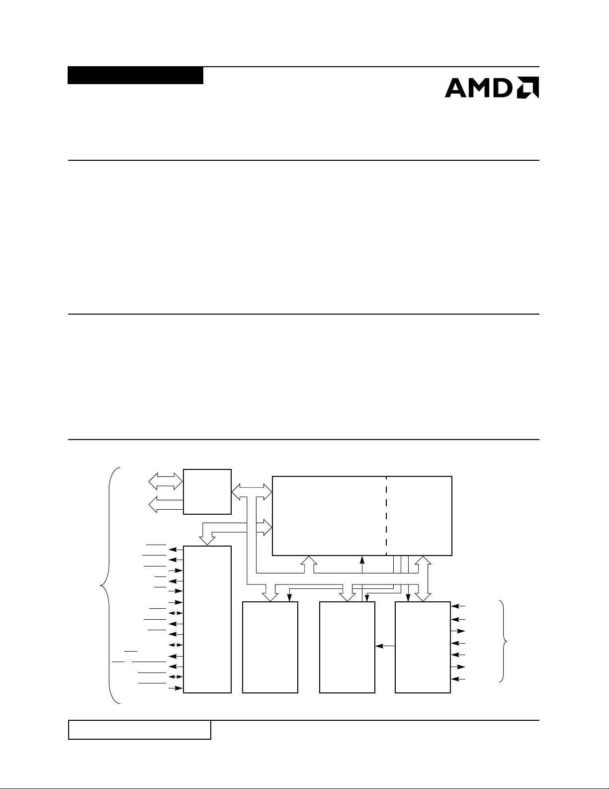
BLOCK DIAGRAM
Parallel
Bus
Interface
C-LANCE/
CPU
Control
Bus
Interface
Station
Address
Detection
Local CPU Interface
DAL15:0
A23:16
BM
1/BUSAKO
BM
INTR
HOLD
HLDA
ALE/AS
CS
ADR
AS
D
DALO
DALI
READ
0/BYTE
READY
RESET
to provide the user with a complete interface module for
an Ethernet network. The Am79C90 is designed using
a scalable CMOS technology and is compatible with a
variety of microprocessors. On-board DMA, advanced
buffer management, and extensive error reporting and
diagnostics facilitate design and improve system
performance.
DMA/Data
Path Control
Retry
Logic
Microprogram
Store
Serial I/O
Interface
RX
RCLK
TX
TCLK
CLSN
TENA
RENA
17881C-1
Am7992B SIA Interface
Publication# 17881 Rev: CAmendment/0
Issue Date: January 1998
This document contains information on a product under development at Advanced Micro Devices. The
information is intended to help you evaluate this product. AMD reserves the right to change or discontinue
work on this proposed product without notice.
1
Page 2
AMD
P R E L I M I N A R Y
RELATED AMD PRODUCTS
Part No. Description
Am7996 IEEE 802.3/Ethernet/Cheapernet Tap Transceiver
Am79C100 Twisted-Pair Ethernet Transceiver Plus (TPEX+)
TM
TM
(ILACCTM)
)
Am79C900 Integrated Local Area Communications Controller
Am79C940 Media Access Controller for Ethernet (MACE
Am79C960 PCnet-ISA Single-Chip Ethernet Controller (for ISA bus)
Am79C961 PCnet-ISA Single-Chip Ethernet Controller (with Microsoft
Plug n’ Play support)
Am79C965 PCnet-32 Single-Chip 32-Bit Ethernet Controller (for 386DX, 486 and VL buses)
Am79C970 PCnet-PCI Single-Chip Ethernet Controller (for PCI bus)
Am79C974 PCnet-SCSI Combination Ethernet and SCSI Controller for PCI Systems
Am79C98 Twisted-Pair Ethernet Transceiver (TPEX)
TM
Am79C981 Integrated Multiport Repeater Plus
Am79C987 Hardware Implemented Management Information Base
(IMR+TM)
TM
(HIMIBTM)
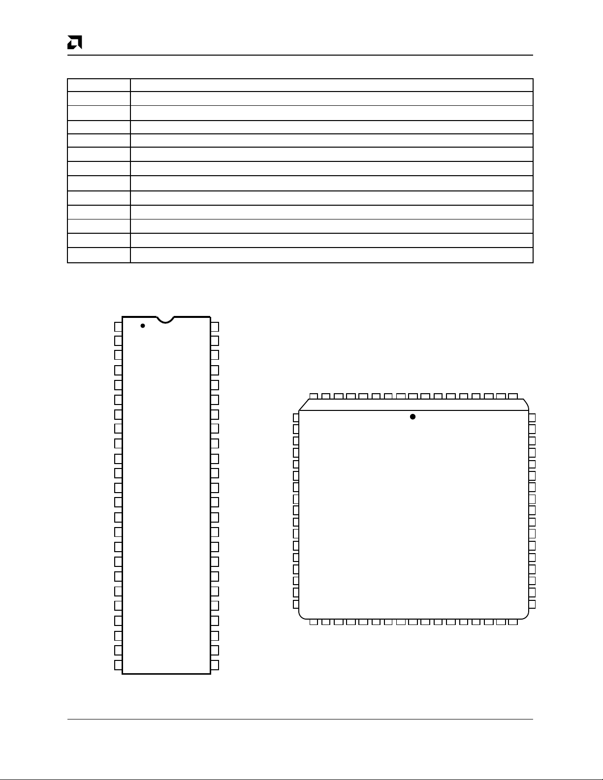
CONNECTION DIAGRAMS
DIP PLCC
1
V
SS
DAL7
DAL6
DAL5
DAL4
DAL3
DAL2
DAL1
DAL0
READ
INTR
DALI
DALO
DAS
BM0/BYTE
BM1/BUSAKO
HOLD/BUSRQ
ALE/AS
HLDA
ADR
READY
RESET
V
CS
SS
2
3
4
5
6
7
8
9
10
11
12
13
14
15
16
17
18
19
20
21
22
23
24
Note:
Pin 1 is marked for orientation.
48
47
46
45
44
43
42
41
40
39
38
37
36
35
34
33
32
31
30
29
28
27
26
25
17881B-2
V
DD
DAL8
DAL9
DAL10
DAL11
DAL12
DAL13
DAL14
DAL15
A16
A17
A18
A19
A20
A21
A22
A23
RX
RENA
TX
CLSN
RCLK
TENA
TCLK
NC
NC
DAL2
DAL3
DAL4
DAL5
DAL6
DAL7
VSS
VDD
DAL8
DAL9
DAL10
DAL11
DAL12
NC
NC
10
11
12
13
14
15
16
17
18
19
20
21
22
23
24
25
26
DAL1
DAL0
NC
NC
READ
7
29
DAL13
INTR
6
30
DAL14
DALI
5
31
DAL15
4
32
DALO
NC
3
33
A16
A17
NC
DAS
NCNCBM1/BUSRQ
BM0/BYTE
1
67
68
36
NC
37
66
38
NC
298
35
342728
A18
A19
65
39
A20
64
40
A21
HOLD/BUSRQ
ALE/AS
63
41
42
A22
A23
HLDA
62
61
43
RX
17881B-3
NC
60
59
58
57
56
55
54
53
52
51
50
49
48
47
46
45
44
RENA
NC
CS
NC
NC
ADR
READY
RESET
NC
NC
VSS
TCLK
TENA
RCLK
CLSN
TX
NC
NC
2
Am79C90
Page 3
PRELIMINARY
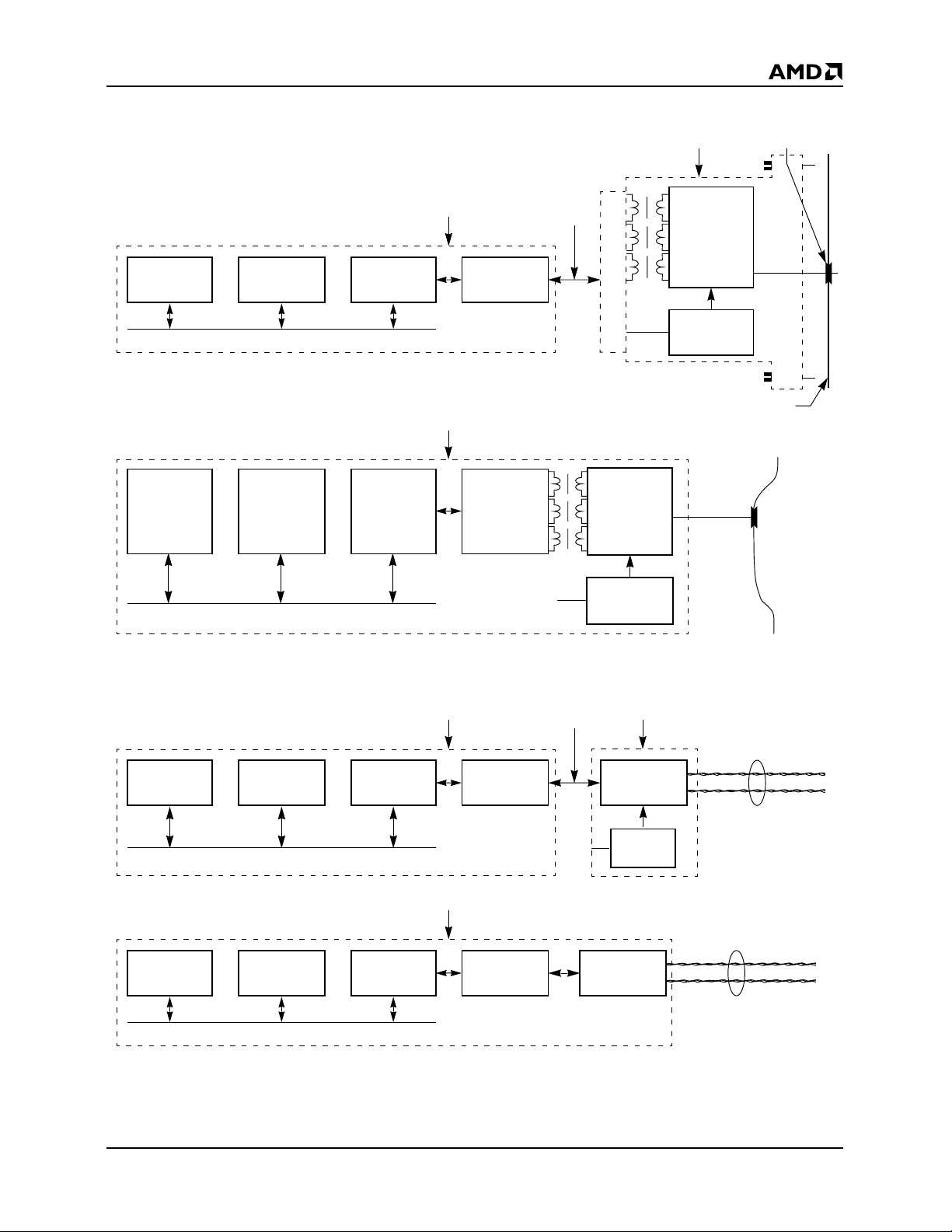
TYPICAL ETHERNET/CHEAPERNET NODE
Ethernet
Local
CPU
Cheapernet
Local
CPU
Local
Memory
Local Bus
Local
Memory
Local Bus
Am79C90
C-LANCE
Am79C90
C-LANCE
DTE
DTE
Am7992B
SIA
Am7992B
SIA
AUI
Cable
Am7996
Transceiver
Power
Supply
MAU
Am7996
Transceiver
Power
Supply
Ethernet Coax
TAP
RG58A/U or
RG58C/U
BNC “T”
Typical Ethernet 10BASE-T Node
Local
CPU
Local
CPU
Local
Memory
Local Bus
Local
Memory
Local Bus
Am79C90
C-LANCE
Am79C90
C-LANCE
DTE
Am7992B
SIA
DTE
Am7992B
SIA
AUI
Cable
MAU
Am79C98
Am79C100
Power
Supply
Am79C98
Am79C100
Twisted-Pair
AUI—Attachment Unit Interface DTE—Data Terminal Equipment MAU—Medium Attachment Unit
Twisted-Pair
17881C-4
Am79C90 3
Page 4
PRELIMINARY
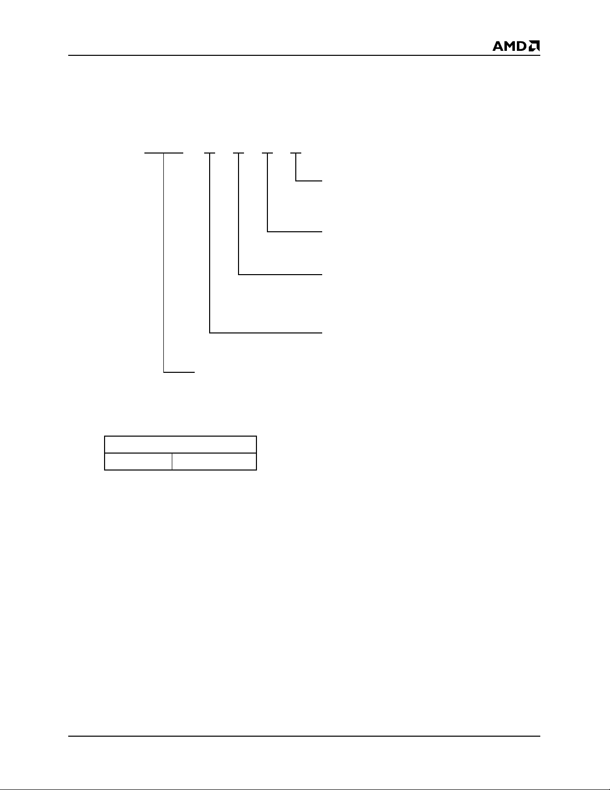
ORDERING INFORMATION
Standard Products
AMD standard products are available in several packages and operating ranges. The order number (valid combination) is formed
by a combination of the elements below.
AM79C90 P C
DEVICE NUMBER/DESCRIPTION
Am79C90
CMOS Local Area Network Controller for Ethernet
B
OPTIONAL PROCESSING
Blank=Standard Processing
TR=Tape and Reel Packaging
OPERATING CONDITIONS
C = Commercial (0°C to +70°C)
PACKAGE TYPE
P=48-Pin Plastic DIP (PD 048)
J=68-Pin Plastic Leaded Chip Carrier (PL 068)
SPEED
Not Applicable
Valid Combinations
AM79C90 PC, JC, JCTR
Valid Combinations
Valid combinations list configurations planned to be supported in volume for this device. Consult the local AMD sales
office to confirm availability of specific valid combinations and
to check on newly released combinations.
4 Am79C90
Page 5
PRELIMINARY
PIN DESCRIPTION
A16–A23
High Order Address Bus (Output, Three-State)
Additional address bits to access a 24-bit address.
These lines are driven as a Bus Master only.
ADR
Register Address Port Select (Input)
When the C-LANCE is a Slave, ADR indicates which of
the two register ports is selected. ADR LOW selects
register data port; ADR HIGH selects register address
port. ADR must be valid throughout the data portion of
the bus cycle and is only used by the C-LANCE when
is LOW.
CS
ALE/AS
Address Latch Enable (Output, Three-State)
Used to demultiplex the DAL lines and define the
address portion of the bus cycle. This l/O pin is programmable through bit (01) of CSR3.
As ALE (CSR3 (01), ACON = 0), the signal transitions
from a HIGH to a LOW during the address portion of
the transfer and remains LOW during the data portion.
ALE can be used by a Slave device to control a latch on
the bus address lines. When ALE is HIGH, the latch is
open, and when ALE goes LOW, the latch is closed.
(CSR3 (01), ACON = 1), the signal pulses LOW
As AS
during the address portion of the bus transaction. The
LOW-to-HlGH transition of AS can be used by a Slave
device to strobe the address into a register.
The C-LANCE drives the ALE/AS line only as a Bus
Master.
BM0/BYTE, BM
(Output, Three-State)
The two pins are programmable through bit (00) of
CSR3.
0, BM1—If CSR3 (00) BCON = 0
BM
PIN 15 = BM0 (Output, Three-State) (48-Pin DlPs)
PIN 16 = BM1 (Output, Three-State) (48-Pin DlPs)
BM0, BM1 (Byte Mask). This indicates that the byte(s)
on the DAL are to be read or written during this bus
transaction. The C-LANCE drives these lines only as a
Bus Master. It ignores the Byte Mask lines when it is a
Bus Slave and assumes word transfers.
1
/BUSAKO
Byte selection using Byte Mask is done as described
by the following table:
BM
1
LOW LOW Whole Word
LOW HIGH Upper Byte
HlGH LOW Lower Byte
HlGH HIGH None
BYTE, B
PIN 15 = BYTE (Output, Three-State) (48-Pin DlPs)
PIN 16 = BUSAKO (Output) (48-Pin DIPs)
Byte selection may also be done using the BYTE line
and DAL00 line, latched during the address portion of
the bus cycle. The C-LANCE drives BYTE only as a
Bus Master and ignores it when a Bus Slave selection
is done (similar to BM0, BM1). Byte selection is done
as outlined in the following table:
B
is not requesting the bus and it receives HLDA,
BUSAKO will be driven LOW. If the C-LANCE is requesting the bus when it receives HLDA, BUSAKO will
remain HIGH.
USAKO—If CSR3 (00) BCON = 1
BYTE DAL
LOW LOW Whole Word
LOW HIGH Illegal Condition
HlGH LOW Lower Byte
HlGH HIGH Upper Byte
USAKO is a bus request daisy chain output. If the chip
BM
0
00
Selection
Selection
Byte Swapping
In order to be compatible with the variety of 16-bit microprocessors available to the designer, the C-LANCE
may be programmed to swap the position of the upperand lower-order bytes on data involved in transfers with
the internal FIFOs.
Byte swapping is done when BSWP = 1. The most
significant byte of the word in this case will appear on
DAL lines 7–0 and the least significant byte on DAL
lines 15–8.
When BYTE = H (indicating a byte transfer) the table indicates on which part of the 16-bit data bus the actual
data will appear.
Whenever byte swap is activated, the only data that is
swapped is data traveling to and from the Transmit/
Receive FIFOs.
Am79C90 5
Page 6
PRELIMINARY
Mode Bits
Signal Line
BYTE = L and
DAL00 = L
BYTE = L and
DAL00 = H
BYTE = H and
DAL00 = H
BYTE = H and
DAL00 = L
BSWP = 0
and BCON = 1
Word Word
Illegal Illegal
Upper Byte Lower Byte
Lower Byte Upper Byte
BSWP = 1
and BCON = 1
CLSN
Collision (Input)
A logical input that indicates that a collision is occurring
on the channel.
CS
Chip Select (Input)
Indicates, when asserted, that the C-LANCE is the
Slave device of the data transfer. CS
throughout the data portion of the bus cycle. CS must
not be asserted when HLDA is LOW.
must be valid
DAL00–DAL15
Data/Address Lines (Input/Output, Three-State)
The time multiplexed Address/Data bus. During the address portion of a memory transfer, DAL00–DAL15
contains the lower 16 bits of the memory address. The
upper 8 bits of address are contained in A16–A23.
During the data portion of a memory transfer, DAL00–
DAL15 contains the read or write data, depending on
the type of transfer.
The C-LANCE drives these lines as a Bus Master and
as a Bus Slave.
D
ALI
Data/Address Line In (Output, Three-State)
An external bus transceiver control line. D
serted when the C-LANCE reads from the DAL lines. It
will be LOW during the data portion of a READ transfer
and remain HIGH for the entire transfer if it is a WRITE.
DALI is driven only when C-LANCE is a Bus Master.
D
ALO
Data/Address Line Out (Output, Three-State)
An external bus transceiver control line. D
serted when the C-LANCE drives the DAL lines. DALO
will be LOW only during the address portion if the transfer is a READ. It will be LOW for the entire transfer if the
transfer is a WRITE. DALO is driven only when
C-LANCE is a Bus Master.
ALI is as-
ALO is as-
DAS
Data Strobe (Input/Output, Three-State)
Defines the data portion of the bus transaction. D
high during the address portion of a bus transaction
and low during the data portion. The LOW-to-HlGH
transition can be used by a Slave device to strobe bus
data into a register. DAS is driven only as a Bus Master.
AS is
HLDA
Bus Hold Acknowledge (Input)
A response to HOLD
to the chip’s assertion of HOLD, the chip is the Bus
Master.
During Bus Master operation, the C-LANCE waits for
A to be deasserted HIGH before reasserting
HLD
HOLD LOW. This insures proper bus handshake under
all situations.
. When HLDA is LOW in response
HOLD/BUSRQ
Bus Hold Request (Output, Open Drain)
Asserted by the C-LANCE when it requires access to
memory. HOLD
transaction. The function of this pin is programmed
through bit (00) of CSR3. Bit (00) of CSR3 is cleared
when RESET is asserted.
When CSR3 (00) BCON = 0
PIN 17 = HOLD
(Output Open Drain and input sense) (48-Pin DIPs)
When CSR3 (00) BCON = 1
PIN 17 = BUSRQ (I/O Sense, Open Drain) (48-Pin DlPs)
If the C-LANCE wants to use the bus, it looks at HOLD/
BUSRQ; if it is HIGH the C-LANCE can pull it LOW and
request the bus. If it is already LOW, the C-LANCE
waits for it to go inactive-HlGH before requesting the
bus.
is held LOW for the entire ensuing bus
INTR
Interrupt (Output, Open Drain)
An attention signal that indicates, when active, that one
or more of the following CSR0 status flags is set: BABL,
MERR, MISS, RINT, TINT or IDON. INTR
bit 06 of CSR0 (INEA = 1). INTR remains asserted until
the source of Interrupt is removed.
is enabled by
RCLK
Receive Clock (Input)
A 10 MHz square wave synchronized to the Receive
data and only active while receiving an Input Bit
Stream.
6 Am79C90
Page 7

PRELIMINARY
READ
(Input/Output, Three-State)
Indicates the type of operation to be performed in the
current bus cycle. This signal is an output when the
C-LANCE is a Bus Master.
High—Data is taken off the DAL lines by the
C-LANCE.
Low—Data is placed on the DAL lines by the
C-LANCE.
The signal is an input when the C-LANCE is a Bus
Slave.
High—Data is placed on the DAL lines by the
C-LANCE.
Low—Data is taken off the DAL lines by the
C-LANCE.
READY
(Input/Output, Open Drain)
When the C-LANCE is a Bus Master, READ
asynchronous acknowledgment from the bus memory
that it will accept data in a WRITE cycle or that it has
put data on the DAL lines in a READ cycle.
As a Bus Slave, the C-LANCE asserts READY when it
has put data on the DAL lines during a READ cycle or
is about to take data off the DAL lines during a write
cycle. READY is a response to DAS and will return High
after DAS has gone High. READY is an input when the
C-LANCE is a Bus Master and an output when the
C-LANCE is a Bus Slave.
Y is an
RENA
Receive Enable (Input)
A logical input that indicates the presence of carrier on
the channel.
RESET
Reset (Input)
Reset causes the C-LANCE to cease operation, clear
its internal logic, force all three-state buffers to the highimpedance state, and enter an idle state with the stop
bit of CSR0 set. It is recommended that a 3.3 k Ω pullup
resistor be connected to this pin.
RX
Receive (Input)
Receive Input Bit Stream.
TCLK
Transmit Clock (Input)
10 MHz clock.
TENA
Transmit Enable (Output)
Transmit Output Bit Stream enable. When asserted, it
enables valid transmit output (TX).
TX
Transmit (Output)
Transmit Output Bit Stream.
V
DD
Power Supply Pin +5 V ± 5%
It is recommended that 0.1 µ F and 10 µ F decoupling
capacitors be used between V
V
SS
Ground
Pin 1 and 24 (48-Pin DlPs) should be connected
together externally, as close to the chip as possible.
DD
and V
SS
.
Am79C90 7
Page 8
AMD
P R E L I M I N A R Y
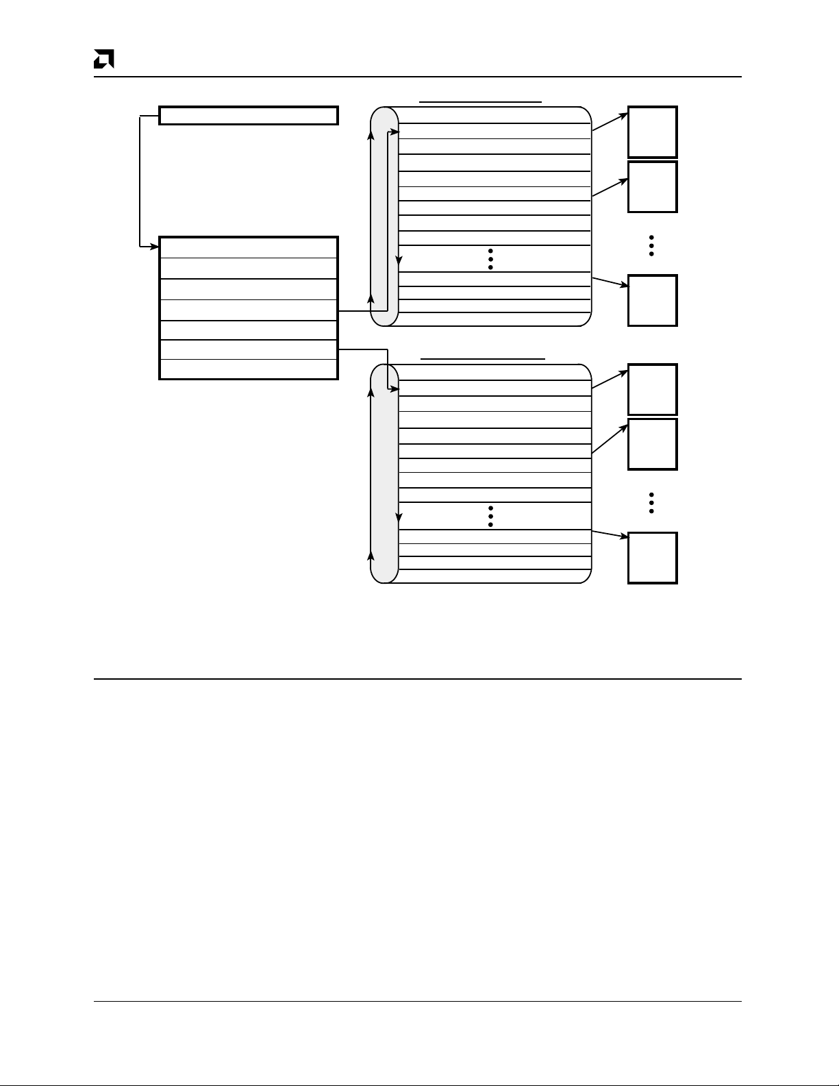
FUNCTIONAL DESCRIPTION
The parallel interface of the CMOS Local Area Network
Controller for Ethernet (C-LANCE) has been designed
to be “friendly” or easy to interface to a variety of popular
microprocessors. These microprocessors include the
Am29000, 80x86, 680x0, Z8000 and LSI-11. The
C-LANCE has a 24-bit wide linear address space when
it is in the Bus Master Mode. A programmable mode of
operation allows byte addressing in one of two ways:
aByte/Word control signal compatible with the 80x86
and Z8000 or an Upper Data Strobe and Lower Data
Address
Bits
16–23
A16–A23
CPU
DAL0–DAL15
ALE
Data and
Address
Bits 0–15
Buffer
Buffer
Strobe signal compatible with microprocessors such as
the 68000. A programmable polarity on the Address
Strobe signal eliminates the need for external logic. The
C-LANCE interfaces with both multiplexed and demultiplexed data busses and features control signals for
address/data bus transceivers. The C-LANCE is pin-forpin compatible with AMD’s LANCE device (Am7990).
Please refer to Appendix B for a complete comparison
between the C-LANCE and LANCE devices.
Control
A16–A23
DAL0 – DAL15
Buffer
ALE
A16–A23
DAL0–DAL15A16–A23Control
Figure 1. C-LANCE/CPU Interfacing Multiplexed Bus
Latch
Decoder
C-LANCE
ALE
ADR
CS
17881B-5
8
Am79C90
Page 9
Data Bus
P R E L I M I N A R Y
Address
Bus
Data/Address
Bits 0-15
A0–A15
Latch
A16–A23
Buffer
A0–A23
Decode
ALE
Address
Bits 16-23
C-LANCE
CS
Figure 2. C-LANCE/CPU Interfacing Demultiplexed Bus
AMD
17881B-6
During initialization, the CPU loads the starting address
of the initialization block into two internal control registers. The C-LANCE has four internal control and status
registers (CSR0, 1, 2, 3) which are used for various
functions, such as the loading of the initialization block
address, and programming different modes and status
conditions. The host processor communicates with the
C-LANCE during the initialization phase, for demand
transmission, and periodically to read the status bits following interrupts. All other transfers to and from the
memory are automatically handled as DMA.
Interrupts to the microprocessor are generated by the
C-LANCE upon:
completion of its initialization routine
the reception of a packet
the transmission of a packet
transmitter timeout error
a missed packet
memory error
The cause of the interrupt is ascertained by reading
CSR0. Bit (06) of CSR0, (INEA), enables or disables
interrupts to the microprocessor. In systems where polling is used in place of interrupts, bit (07) of CSR0,
(INTR), indicates an interrupt condition.
The basic operation of the C-LANCE consists of two distinct modes: transmit and receive. In the transmit mode,
the C-LANCE chip directly accesses data (in a transmit
buffer) in memory. It prefaces the data with a preamble,
start frame delimiter (SFD), and calculates and appends
a 32-bit CRC. On transmission, the first byte of data
loads into the 48-byte Transmit FIFO; the C-LANCE
then begins to transmit preamble while simultaneously
loading the rest of the packet into Transmit FIFO for
transmission.
In the receive mode, packets are sent via the Am7992B
SlA to the C-LANCE. The packets are loaded into the
64-byte Receive FIFO for preparation of automatic
downloading into buffer memory. A CRC is calculated
and compared with the CRC appended to the data packet. If the calculated CRC does not agree with the packet
CRC, an error bit is set.
Addressing
Packets can be received using three different destination addressing schemes: physical, logical and
promiscuous.
The first type is a full comparison of the 48-bit destination address in the packet with the node address that
was programmed into the C-LANCE during an initialization cycle. There are two types of logical addresses.
One is group type mask where the 48-bit address in the
packet is put through a hash filter to map the 48-bit
physical addresses into 1 of 64 logical groups. If any of
these 64 groups have been preselected as the logical
address, then the 48-bit address is stored in main memory. At this time, a look up is performed by the host computer comparing the 48-bit incoming address with the
pre-stored 48-bit logical address. This mode can be
useful if sending packets to all of a particular type of device simultaneously (i.e., send a packet to all file servers
or all printer servers). Additional details on logical addressing can be found in the INITIALIZATION section
9Am79C90
Page 10

AMD
P R E L I M I N A R Y
under “Logical Address Filter.” The second logical address is a broadcast address where all nodes on the network receive the packet. The last receive mode of
operation is referred to as “promiscuous mode” in which
a node will accept all packets on the medium regardless
of their destination address.
Collision Detection and Implementation
The Ethernet and IEEE 802.3 CSMA/CD network access algorithms are implemented completely within the
C-LANCE. In addition to listening for a clear medium before transmitting, Ethernet handles collisions in a predetermined way. Should two transmitters attempt to seize
the medium at the same time, they will collide and the
data on the medium will be garbled. The transmitting
nodes listen while they transmit, detect the collision,
then continue to transmit for a predetermined length of
time to “jam” the network and ensure that all nodes have
recognized the collision. The transmitting nodes then
delay a random amount of time according to the Ethernet “truncated binary backoff” algorithm in order that the
colliding nodes do not try to repeatedly access the network at the same time. The C-LANCE also offers a selectable Modified Backoff Algorithm for better
performance on busy networks. Up to 16 attempts to access the network are made by the C-LANCE before reporting an error due to excessive collisions.
Error Reporting and Diagnostics
Extensive error reporting is provided by the C-LANCE.
Error conditions reported relate either to the network as
a whole or to individual data packets. Network-related
errors are recorded as flags in the CSRs and are examined by the CPU following interrupt. Packet-related errors are written into descriptor entries corresponding to
the packet.
System errors include:
Babbling Transmitter
—Transmitter attempting to transmit more than
1518 bytes, excluding preamble and start frame
delimiter
Collision
—Collision detection circuitry nonfunctional
Missed Packet
—Insufficient buffer space
Memory timeout
—Memory response failure
Packet-related errors:
CRC
—Invalid data
Framing
—Packet did not end on a byte boundary
Overflow/Underflow
—Indicates abnormal latency in servicing a DMA
request
Buffer
—Insufficient buffer space available
The C-LANCE performs several diagnostic routines
which enhance the reliability and integrity of the system.
These include a CRC check and two loop back modes
(internal/external). Errors may be introduced into the
system to check error detection logic. A Time Domain
Reflectometer is incorporated into the C-LANCE to aid
system designers in locating faults in the Ethernet physical medium. Shorts and opens manifest themselves in
reflections which are sensed by the TDR.
10
Am79C90
Page 11
P R E L I M I N A R Y
Transmit Descriptor for 1st Data Buffer
Transmit Descriptor for 2nd Data Buffer
Transmit Descriptor for 3rd Data Buffer
Transmit Descriptor for Nth Data Buffer
Receive Descriptor for 1st Data Buffer
Receive Descriptor for 2nd Data Buffer
Receive Descriptor for 3rd Data Buffer
Receive Descriptor for Nth Data Buffer
AMD
Initialization
Block
Transmit
Descriptor
Ring
(4 words
per entry)
Receive
Descriptor
Ring
(4 words
per entry)
Transmit Data Buffer #1
Transmit Data Buffer #2
Transmit Data Buffer #3
Transmit Data Buffer #N
Receive Data Buffer #1
Receive Data Buffer #2
Receive Data Buffer #3
Receive Data Buffer #N
Figure 2-1. C-LANCE/Processor Memory Interface
Transmit
Data
Buffers
Receive
Data
Buffers
17881B-7
11Am79C90
Page 12
AMD
C-LANCE CSR Registers
Pointer to Initialization Block
Initialization
Block
Mode of Operation
Physical Address
Logical Address Filter
Pointer to Receive Ring
Number of Receive Entries (N)
Pointer to Transmit Ring
Number of Transmit Entries (M)
P R E L I M I N A R Y
Receive Descriptor Ring
Address of Receive Buffer 1
Buffer 1 Status
Buffer 1 Byte Count
Buffer 1 Message Count
Transmit Descriptor Ring
Address of Transmit Buffer 1
Buffer 1 Status
Buffer 1 Byte Count
Buffer 1 Error Status
Receive Buffer
Data
Packet
1
Data
2
2
2
2
N
N
N
N
2
2
2
2
Packet
2
Data
Packet
N
Transmit Buffer
Data
Packet
1
Data
Packet
2
Figure 2-2. C-LANCE Memory Management
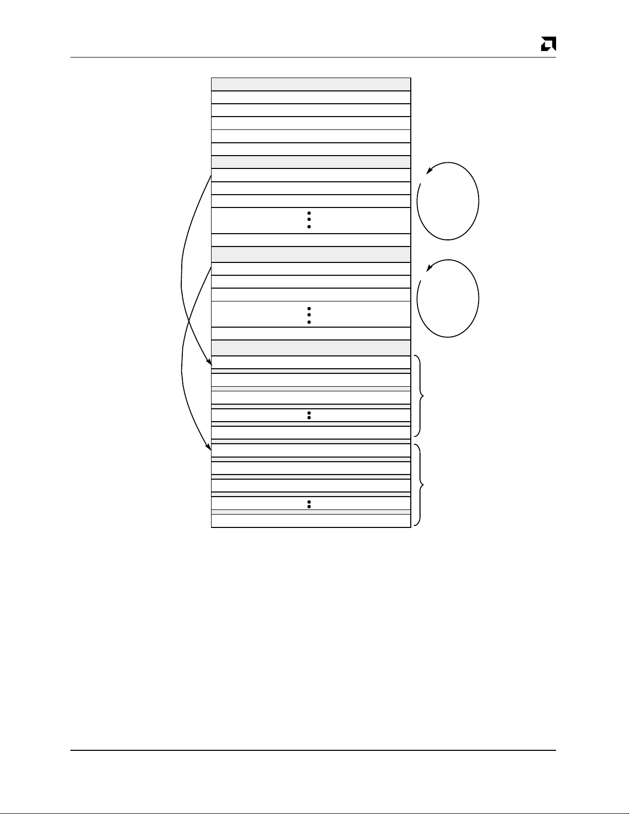
Buffer Management
A key feature of the C-LANCE and its on-board DMA
channel is the flexibility and speed of communication
between the C-LANCE and the host microprocessor
through common memory locations. The basic organization of the buffer management is a circular queue of
tasks in memory called descriptor rings as shown in
Figures 2-1 and 2-2. There are separate descriptor rings
to describe transmit and receive operations. Up to 128
tasks may be queued up on a descriptor ring awaiting
execution by the C-LANCE. Each entry in a descriptor
ring holds a pointer to a data memory buffer and an entry
for the length of the data buffer. Data buffers can be
chained or cascaded to handle a long packet in multiple
data buffer areas. The C-LANCE searches the descriptor rings in a “lookahead” manner to determine the next
empty buffer in order to chain buffers together or to handle back-to-back packets. As each buffer is filled,
M
M
M
M
Data
Packet
M
17881B-8
the“own” bit is reset, allowing the host processor to
process the data in the buffer.
C-LANCE Interface
CSR bits such as ACON, BCON and BSWP are used for
programming the pin functions used for different interfacing schemes. For example, ACON is used to program the polarity of the Address Strobe signal
(ALE/AS).
BCON is used for programming the pins, for handling
either the BYTE/WORD method for addressing word organized, byte addressable memories where the BYTE
signal is decoded along with the least significant address bit to determine upper or lower byte, or an explicit
scheme in which two signals labeled as BYTE MASK
(BM0 and BM1) indicate which byte is addressed. When
12
Am79C90
Page 13

P R E L I M I N A R Y
the BYTE scheme is chosen, the BM1 pin can be used
for performing the function BUSAKO.
BCON is also used to program pins for different DMA
modes. In a daisy chain DMA scheme, 3 signals are
used (BUSRQ, HLDA, BUSAKO). In systems using a
DMA controller for arbitration, only HOLD and HLDA are
used.
C-LANCE in Bus Slave Mode
The C-LANCE enters the Bus Slave Mode whenever CS
becomes active. This mode must be entered whenever
writing or reading the four status control registers
(CSR0, CSR1, CSR2, and CSR3) and the Register Address Pointer (RAP). RAP and CSR0 may be read or
written to at anytime, but the C-LANCE must be stopped
(by setting the stop bit in CSR0) for CSR1, CSR2, and
CSR3 access.
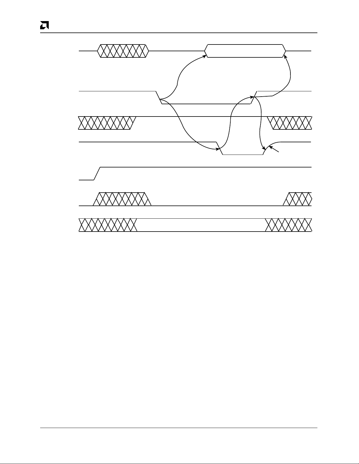
Read Sequence (Slave Mode)
At the beginning of a read cycle, CS, READ, and DAS
are asserted. ADR must be valid at this time. (If ADR is a
“1,” the contents of RAP are placed on the DAL lines.
Otherwise the contents of the CSR register addressed
by RAP are placed on the DAL lines.) After the data on
the DAL lines become valid, the C-LANCE asserts
READY, CS, READ, DAS, and ADR must remain stable
throughout the cycle. Refer to Figure 3.
AMD
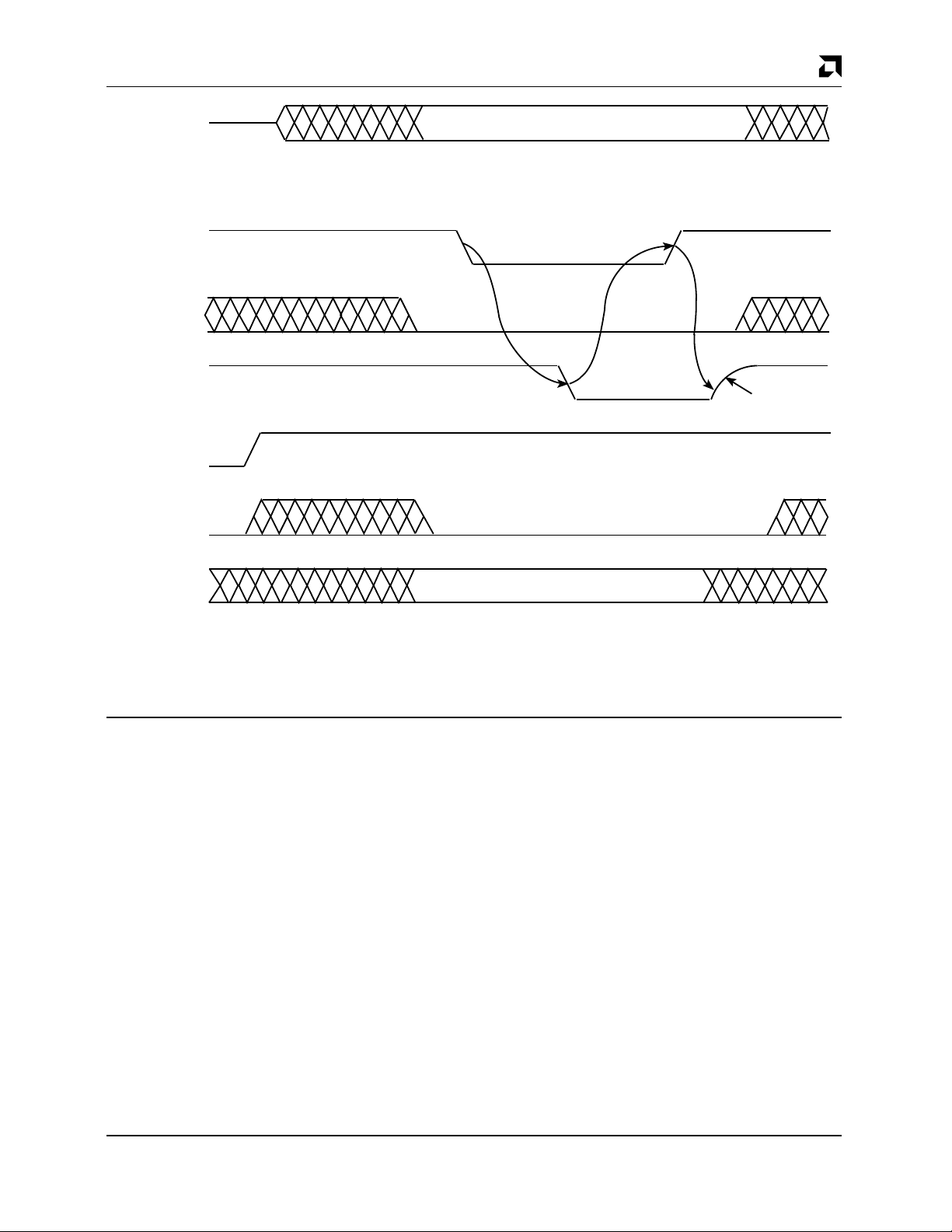
Write Sequence (Slave Mode)
This cycle is similar to the read cycle, except that during
this cycle, READ is not asserted (READ is LOW). The
DAL buffers are tristated which configures these lines as
inputs. The assertion of READY by C-LANCE indicates
to the memory device that the data on the DAL lines
have been stored by C-LANCE in its appropriate CSR
register. CS, READ, DAS, ADR and DAL 15:00 must remain stable throughout the write cycle. Refer to
Figure4.
Note: Setting the STOP bit in the C-LANCE will generate a C-LANCE reset, which will cause all bus control
output signals (including
READY
) to float. To guarantee
slave write timing when the STOP bit is being set in
CSR0, the C-LANCE will latch the STOP bit and will wait
for the slave cycle to complete before resetting itself and
floating the output signals.
C-LANCE in Bus Master Mode
All data transfers from the C-LANCE in the bus Master
mode are timed by ALE, DAS, and READY. The automatic adjustment of the C-LANCE cycle by the READY
signal allows synchronization with variable cycle time
memory due either to memory refresh or to dual port access. Transfers are a minimum of 600 ns in length except for the first transfer of a bus mastership period in
which the minimum is 700 ns. Transfers can be increased in 100ns increments.
13Am79C90
Page 14
AMD
DAL0–DAL15
DAS
READ
READY
(Output from
C-LANCE)
HOLD
P R E L I M I N A R Y
Read Data
See
Note 1
O.D.
CS
ADR
Note:
1. There are two types of delays which depend on which internal register is accessed.
Type 1 refers to access of CSR0, CSR3 and RAP.
Type 2 refers to access of CSR1 and CSR2 which are longer than Type 1 delay.
Figure 3. Bus Slave Read Timing
17881B-9
14
Am79C90
Page 15
DAL0–DAL15
DAS
READ
READY
(Output from
C-LANCE)
HOLD
CS
P R E L I M I N A R Y
AMD
Write Data
O.D.
ADR
Figure 4. Bus Slave Write Timing
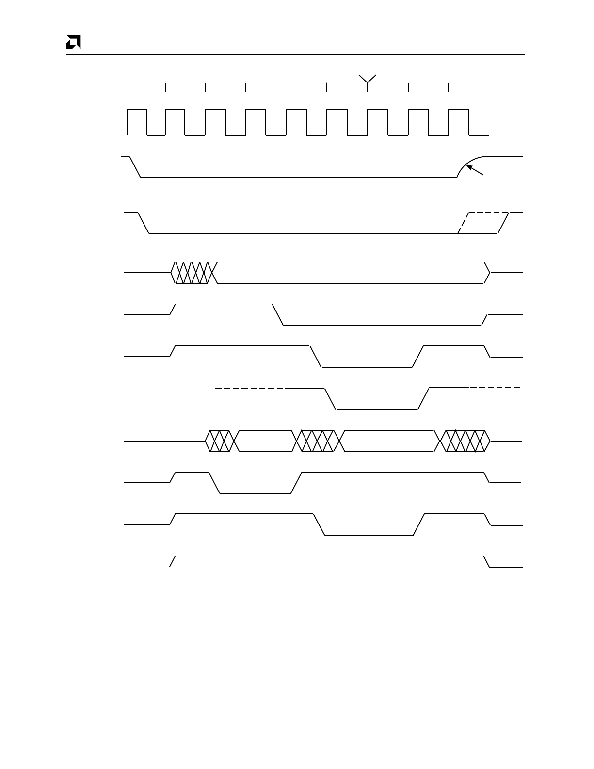
Read Sequence (Master Mode)
A read cycle is begun by placing a valid address on
DAL00 – DAL15 and A16 – A23. The BYTE MASK signals are asserted to indicate a word, upper byte or lower
byte memory reference. READ indicates the type of cycle. ALE or AS is pulsed, and the trailing edge of either
can be used to latch addresses. DAL00 – DAL15 go into
a 3-state mode, and DAS falls LOW to signal the beginning of the memory access. The memory responds by
placing READY LOW to indicate that the DAL lines have
valid data. The C-LANCE then latches memory data on
the rising edge of DAS, which in turn ends the memory
cycle and READY returns HIGH. Refer to Figure 5-1.
17881B-10
The bus transceiver controls, DALI and DALO, are used
to control the bus transceivers. DALI directs data toward
the C-LANCE, and DALO directs data or addresses
away from the C-LANCE. During a read cycle, DALO
goes inactive before DALI becomes active to avoid
“spiking” of the bus transceivers.
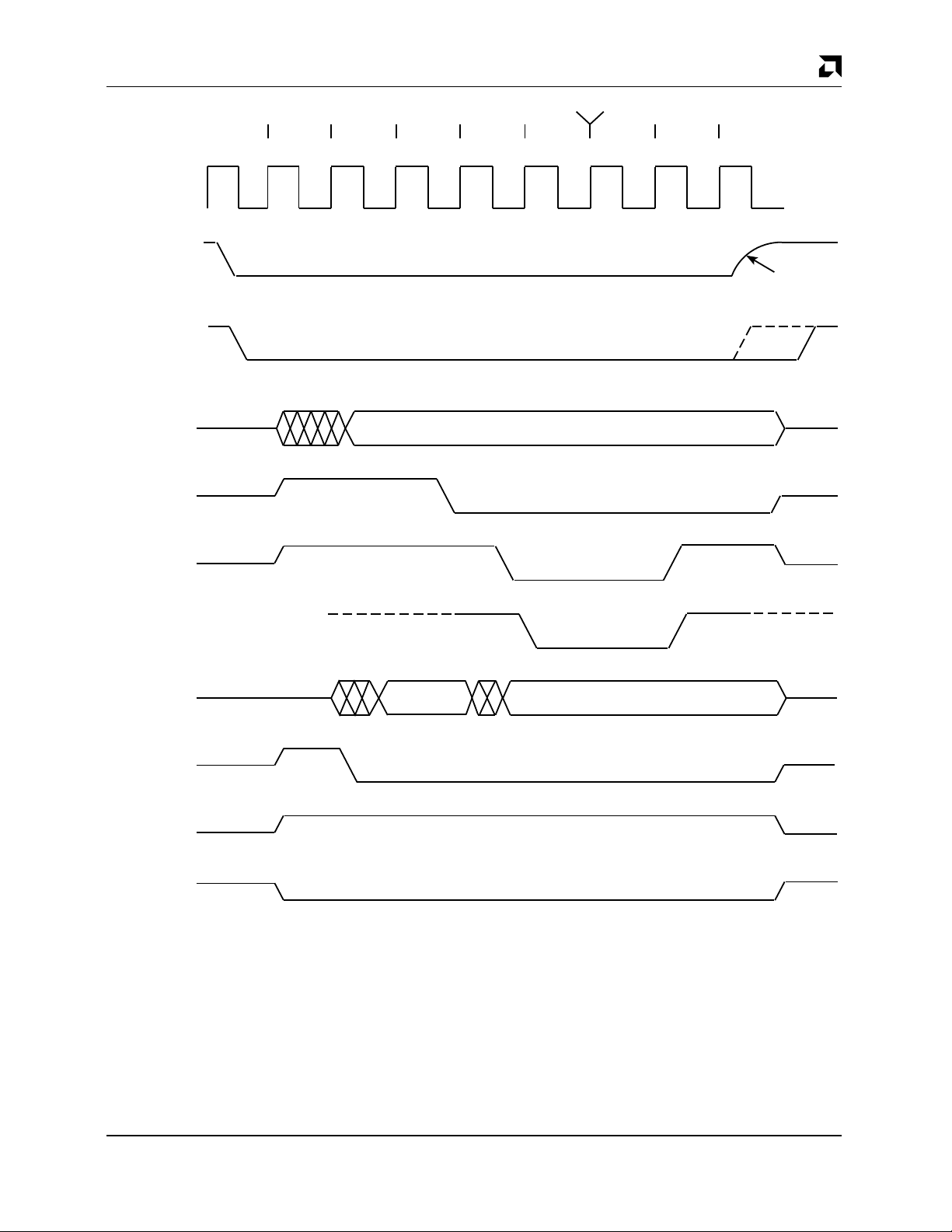
Write Sequence (Master Mode)
The write cycle is similar to the read cycle except that the
DAL00 – DAL15 lines change from containing addresses to data after either ALE or AS goes inactive.
After data is valid on the bus, DAS goes active. Data to
memory is held valid after DAS goes inactive. Refer to
Figure 5-2.
15Am79C90
Page 16
AMD
TCLK
HOLD
HLDA
A16–A23
BM0, BM1
ALE
P R E L I M I N A R Y
T
WAIT
T0
0
T1 T2 T3 T4 T5 T6
100 200 300 400 500
Address, BM0, BM1
600
700
O.D.
DAS
READY
DAL0–DAL15
(Read)
DALO
(Read)
DALI
(Read)
READ
(Read)
Address
Data In
Figure 5-1. Bus Master Read Timing (Single DMA Cycle)
17881B-11
16
Am79C90
Page 17
TCLK
HOLD
HLDA
A16–A23
BM0, BM1
ALE
P R E L I M I N A R Y
T
WAIT
T0
0 100 200 300 400 500 600
T1 T2 T3 T4 T5 T6
Address, BM0, BM1
AMD
700
O.D.
DAS
READY
DAL0–DAL15
(Write)
DALO
(Write)
DALI
(Write)
READ
(Write)
Address
Data Out
Figure 5-2. Bus Master Write Timing (Single DMA Cycle)
17881B-12
17Am79C90
Page 18
AMD
P R E L I M I N A R Y
Differences Between Ethernet Versions 1
and 2
a.Version 2 specifies that the collision detect of the
transceiver must be activated during the interpacket gap time.
b.Version 2 specifies some network management
functions, such as reporting the occurrence of collisions, retries and deferrals.
c.Version 2 specifies that when transmission is ter-
minated, the differential transmit lines are driven to
0 volt differentially (half step).
Differences Between IEEE 802.3 and
Ethernet
a.IEEE 802.3 specifies a 2-byte length field rather
than a type field. The length field (802.3) describes
the actual amount of data in the frame.
b.IEEE 802.3 allows the use of a PAD field in the
data section of a frame, while Ethernet specifies
the minimum packet size at 64 bytes. The use of a
PAD allows the user to send and receive packets
which have less than 46 bytes of data.
A list of significant differences between Ethernet and
IEEE 802.3 at the physical layer include the following:
IEEE 802.3 Ethernet
End of Transmission Half Step Full Step (Rev 1)
State or
Half Step (Rev 2)
Common Mode Voltage ±5.5 V 0 – +5 V
Common Mode CurrentLess than 1 mA 1.6 mA ±40%
Receive±, Collision±
Input Threshold ±160 mV ±175 mV
Fault Protection 16 V 0 V
18
Am79C90
Page 19

P R E L I M I N A R Y
PROGRAMMING
This section defines the Control and Status Registers
and the memory data structures required to program the
Am79C90 (C-LANCE).
Programming the Am79C90 (C-LANCE)
The Am79C90 (C-LANCE) is designed to operate in an
environment that includes close coupling with local
memory and microprocessor (HOST). The Am79C90
C-LANCE is programmed by a combination of registers
and data structures resident within the C-LANCE and
memory registers. There are four Control and Status
Registers (CSRs) within the C-LANCE which are programmed by the HOST device. Once enabled, the
C-LANCE has the ability to access memory locations to
acquire additional operating parameters.
The Am79C90 has the ability to do independent buffer
management as well as transfer data packets to and
from the Ethernet. There are three memory structures
accessed by the Chip:
Initialization Block—12 words in contiguous memory starting on a word boundary. It also contains
the operating parameters necessary for device operation. The initialization block is comprised of:
—Mode of Operation
—Physical Address
—Logical Address Mask
—Location to Receive and Transmit Descriptor
Rings
—Number of Entries in Receive and Transmit
Descriptor Rings
Receive and Transmit Descriptor Rings—Two ring
structures, one for incoming and outgoing packets.
Each entry in the rings is 4 words long and each
entry must start on a quadword boundary. The Descriptor Rings are comprised of:
—The address of a data buffer
—The length of that data buffer
—Status information associated with the buffer
Data Buffers—Contiguous portions of memory
reserved for packet buffering. Data buffers may
begin on arbitrary byte boundaries.
In general, the programming sequence of the C-LANCE
may be summarized as:
Program the C-LANCE’s CSRs by a host device to
locate an initialization block in memory. The byte
control, byte address, and address latch enable
modes are also defined here.
AMD
The C-LANCE loads itself with the information contained within the initialization block.
The C-LANCE accesses the descriptor rings for
packet handling.
CONTROL AND STATUS REGISTERS
There are four Control and Status Registers (CSRs) on
the chip. The CSRs are accessed through two bus addressable ports, an address port (RAP) and a data port
(RDP).
Accessing the Control and Status
Registers
The CSRs are read (or written) in a two step operation.
The address of the CSR to be accessed is written into
the RAP during a bus slave transaction. During a subsequent bus slave transaction, the data being read from
(or written into) the RDP is read from (or written into) the
CSR selected in the RAP.
Once written, the address in RAP remains unchanged
until rewritten.
To distinguish the data port from the address port, a discrete input pin is provided.
ADR Input Pin Port
L Register Data Port (RDP)
H Register Address Port (RAP)
Register Data Port (RDP)
CSR DATA
17881B-13
Bit Name Description
15:00 CSR Data Writing data into RDP writes the data
into the CSR selected in RAP. Reading the data from the RDP reads the
data from the CSR selected in RAP.
CSR
1, CSR2 and CSR3 are acces-
sible only when the STOP bit of
CSR
0 is set.
If the STOP bit is not set while attempting to access CSR
CSR
3, the C-LANCE will return
READY, but a READ operation will
return undefined data. WRITE operation is ignored.
1, CSR2 or
015
19Am79C90
Page 20

AMD
P R E L I M I N A R Y
Register Address Port (RAP)
CSR 1:0
RES
17881B-14
Bit Name Description
15:02 RES Reserved. Read as zeroes. Write as
zeroes.
01:00 CSR(1:0) CSR address select. READ/WRITE.
Selects the CSR to be accessed
through the RDP. RAP is cleared by
Bus RESET.
CSR(1 :0) CSR
00 CSR
0
01 CSR1
10 CSR2
11 CSR3
Control and Status Register Definition
Control and Status Register 0 (CSR0)
15 0
ERR
BABL
CERR
MISS
MERR
RINT
TINT
IDON
The C-LANCE updates CSR0 by logical “ORing” the previous and present value of CSR
0.
Bit Name Description
INIT
STRT
STOP
TDMD
TXON
RXON
INEA
INTR
17881B-15
Bit Name Description
14 BABL BABBLE is a transmitter timeout er-
ror. It indicates that the transmitter
has been on the channel longer than
the time required to send the maximum length packet.
BABL is a flag which indicates excessive length in the transmit buffer.
It will be set after 1519 bytes have
been transmitted, excluding preamble and start frame delimiter; the
C-LANCE will continue to transmit
until the whole packet is transmitted
or until there is a failure before the
whole packet is transmitted. When
BABL error occurs, an interrupt will
be generated if INEA = 1.
BABL is READ/CLEAR ONLY and is
set by the C-LANCE, and cleared by
writing a “1” into the bit. Writing a ”0”
has no effect. It is cleared by RESET
or by setting the STOP bit.
13 CERR COLLISION ERROR indicates that
the collision input to the C-LANCE
was not asserted during the transmission, nor within 4.0
µs after the
transmit completed. The collision after transmission is a transceiver test
feature. This function is also known
as heartbeat or SQE (Signal Quality
Error) test.
CERR is READ/CLEAR ONLY and
is set by the C-LANCE and cleared
by writing a “1” into the bit. Writing a
“0” has no effect. It is cleared by RE-
SET or by setting the STOP bit.
CERR error will not cause an interrupt to occur (INTR = 0).
12 MISS MISSED PACKET is set when the
receiver loses a packet because it
does not own any receive buffer, indicating loss of data.
FIFO overflow is not reported because there is no receive ring entry
in which to write status.
When MISS is set, an interrupt will
be generated if INEA = 1.
MISS is READ/CLEAR ONLY, and is
set by the C-LANCE and cleared by
writing a “1” into the bit. Writing a “0”
has no effect. It is cleared by RESET
or by setting the STOP bit.
15 ERR ERROR summary is set by the
“ORing” of BABL, CERR, MISS and
MERR. ERR remains set as long as
any of the error flags are true.
ERR is read only; writing it has no effect. It is cleared by Bus RESET, setting the STOP bit, or clearing the
individual error flags.
20
Am79C90
Page 21

P R E L I M I N A R Y
Bit Name Description
11 MERR MEMORY ERROR is set when the
10 RINT RECEIVER INTERRUPT is set
09 TINT TRANSMITTER INTERRUPT is set
08 IDON INITIALIZATION DONE indicates
C-LANCE is the Bus Master and has
not received READY within 25.6
µs
after asserting the address on the
DAL lines.
When a Memory Error is detected,
the receiver and transmitter are
turned off (CSR
0, TXON = 0, RXON
= 0) and an interrupt is generated if
INEA = 1.
MERR is READ/CLEAR ONLY, and
is set by the C-LANCE and cleared
by writing a “1” into the bit. Writing a
“0” has no effect. It is cleared by
RESET or by setting the STOP bit.
when the C-LANCE updates an entry in the Receive Descriptor Ring for
the last buffer received or reception
is stopped due to a failure.
When RINT is set, an interrupt is
generated if INEA = 1.
RINT is READ/CLEAR ONLY, and is
set by the C-LANCE and cleared by
writing a “1” into the bit. Writing a “0”
has no effect. It is cleared by RESET
or by setting the STOP bit.
when the C-LANCE updates an entry in the transmit descriptor ring for
the last buffer sent or transmission is
stopped due to a failure.
When TINT is set, an interrupt is
generated if INEA = 1.
TINT is READ/CLEAR ONLY and is
set by the C-LANCE and cleared by
writing a “1” into the bit. Writing a “0”
has no effect. It is cleared by RESET
or by setting the STOP bit.
that the C-LANCE has completed
the initialization procedure started
by setting the INIT bit. When IDON is
set, the C-LANCE has read the Initialization Block from memory and
stored the new parameters.
When IDON is set, an interrupt is
generated if INEA = 1.
IDON is READ/CLEAR ONLY, and is
set by the C-LANCE and cleared by
writing a “1” into the bit. Writing a “0”
has no effect. It is cleared by RESET
or by setting the STOP bit.
AMD
Bit Name Description
07 INTR INTERRUPT FLAG is set by the
“ORing” of BABL, MISS, MERR,
RINT, TINT and IDON. If INEA = 1
and INTR = 1, the INTR pin will be
LOW.
INTR is READ ONLY; writing this bit
has no effect. INTR is cleared by
RESET, by setting the STOP bit, or
by clearing the condition causing the
interrupt.
06 INEA INTERRUPT ENABLE allows the
INTR pin to be driven LOW when the
Interrupt Flag is set. If INEA = 1 and
INTR = 1, the INTR pin will be Low. If
INEA = 0, the INTR pin will be HIGH,
regardless of the state of the Interrupt Flag.
INEA is READ/WRITE and cleared
by RESET or by setting the STOP
bit.
INEA can be set at any time, regardless of the state of the STOP bit.
(reference Appendix B).
05 RXON RECEIVER ON indicates that the re-
ceiver is enabled. RXON is set when
STRT is set if DRX = 0 in the MODE
register in the initialization block and
the initialization block has been read
by the C-LANCE by setting the INIT
bit. RXON is cleared when IDON is
set from setting the INIT bit and DRX
= 1 in the MODE register, or a memory error (MERR) has occurred.
RXON is READ ONLY; writing this
bit has no effect. RXON is cleared by
RESET or by setting the STOP bit.
04 TXON TRANSMITTER ON indicates that
the transmitter is enabled. TXON is
set when STRT is set if DTX = 0 in
the MODE register in the initialization block and the INIT bit has been
set. TXON is cleared when IDON is
set and DTX = 1 in the MODE register, or an error, such as MERR,
UFLO or BUFF, has occurred during
transmission.
TXON is READ ONLY; writing this bit
has no effect. TXON is cleared by
RESET or by setting the STOP bit.
21Am79C90
Page 22

AMD
Bit Name Description
03 TDMD TRANSMIT DEMAND, when set,
TDMD is WRITE WITH ONE ONLY
02 STOP STOP disables the C-LANCE from
01 STRT START enables the C-LANCE to
00 INIT INITIALIZE, when set, causes the
causes the C-LANCE to access the
Transmit Descriptor Ring without
waiting for the polltime interval to
elapse. TDMD need not be set to
transmit a packet; it merely hastens
the C-LANCE’s response to a Transmit Descriptor Ring entry insertion by
the host.
and is cleared by the microcode after
it is used. It may read as a “1” for a
short time after it is written because
the microcode may have been busy
when TDMD was set. It is also
cleared by RESET or by setting the
STOP bit. Writing a “0” in this bit has
no effect.
all external activity when set and
clears the internal logic. Setting
STOP is the equivalent of asserting
RESET. The C-LANCE remains inactive and STOP remains set until
the STRT or INIT bit is set. If STRT,
INIT and STOP are all set together,
STOP will override the other bits and
only STOP will be set.
STOP is READ/WRITE WITH ONE
ONLY and set by RESET. Writing a
“0” to this bit has no effect. STOP is
cleared by setting either INIT or
STRT. CSR
when the STOP bit is set.
send and receive packets, perform
direct memory access, and do buffer
management. The STOP bit must be
set prior to setting the STRT bit. Setting STRT clears the STOP bit.
STRT is READ/WRITE and is set
with one only. Writing a “0” into this
bit has no effect. STRT is cleared by
RESET or by setting the STOP bit.
C-LANCE to begin the initialization
procedure and access the Initialization Block. The STOP bit must be set
prior to setting the INIT bit. Setting
INIT clears the STOP bit.
INIT is READ/WRITE WITH “1”
ONLY. Writing a “0” into this bit has
no effect. INIT is cleared by RESET
or by setting the STOP bit.
The C-LANCE latches CSR
a slave read; therefore, the CSR
status bits are guaranteed to be stable for the duration of the CSR
access.
3 must be reloaded
P R E L I M I N A R Y
0 during
Control and Status Register 1 (CSR1)
READ/WRITE: Accessible only when the STOP bit
of CSR
0 is a ONE and RAP = 01.
The C-LANCE preserves the contents of CSR
15 10
Bit Name Description
15:01 IADR The low order 15 bits of the address
of the first word (lowest address) in
the Initialization Block.
00 Must be zero.
1 after STOP.
Control and Status Register 2 (CSR2)
READ/WRITE: Accessible only when the STOP bit
of CSR
0 is a ONE and RAP = 10.
The C-LANCE preserves the contents of CSR
15 0
Bit Name Description
15:08 RES Reserved. Read as zeroes. Write as
07:00 IADR The high order 8 bits of the address
87
zeroes.
of the first word (lowest address) in
the initialization Block.
2 after STOP.
0
0
IADR
‘0’
(15:01)
17881B-16
IADR (23:16)
RES
17881B-17
22
Am79C90
Page 23

P R E L I M I N A R Y
Control and Status Register 3 (CSR3)
CSR3 allows redefinition of the Bus Master interface.
READ/WRITE: Accessible only when the STOP bit
of CSR
0 is ONE and RAP = 11.
3 is cleared by RESET or by
CSR
setting the STOP bit in CSR
15 0213
Bit Name Description
15:03 RES Reserved. Read as zeroes. Write as
02 BSWP BYTE SWAP allows the chip to oper-
01 ACON ALE CONTROL defines the asser-
00 BCON BYTE CONTROL redefines the Byte
zeroes.
ate in systems that consider bits
(15:08) of data to be pointed at an
even address and bits (07:00) to be
pointed at an odd address.
When BSWP = 1, the C-LANCE will
swap the high and low bytes on DMA
data transfers between the Receive
FIFO and bus memory. Only data
from the Receive FIFO transfers is
swapped; the Initialization Block
data and the Descriptor Ring entries
are NOT swapped.
BSWP is READ/WRITE and cleared
by RESET or by setting the STOP bit
in CSR
0.
tive state of ALE when the C-LANCE
is a Bus Master. ACON is READ/
WRITE and cleared by RESET and
by setting the STOP bit in CSR
ACON ALE
0 Asserted HIGH
1 Asserted LOW
Mask and Hold l/O pins. BCON is
READ/WRITE and cleared by
RESET or by setting the STOP bit in
CSR
0.
BCON Pin 16 Pin 15Pin 17
0 BM
1 BUSAKOBYTEBUSRQ
1 BM0 HOLD
0.
BCON
ACON
BSWP
RES
17881B-18
0.
AMD
Initialization
Initialization Block
Chip initialization includes the reading of the initialization block in memory to obtain the operating parameters. The following is a definition of the Initialization
Block.
The Initialization Block is read by the C-LANCE when
the INIT bit in CSR0 is set. The INIT bit should be set before or concurrent with the STRT bit to insure proper parameter initialization and chip operation. After the
C-LANCE has read the Initialization Block, IDON is set
in CSR0 and an interrupt is generated if INEA = 1.
Higher Address TLEN–TDR (23:16) IADR +22
TDRA (15:00) IADR +20
RLEN–RDRA (23:16)IADR +18
RDRA (15:00) IADR +16
LADRF (63:48) IADR +14
LADRF (47:32) IADR +12
LADRF (31:16) IADR +10
LADRF (15:00) IADR +08
PADR (47:32) IADR +06
PADR (31:16) IADR +04
PADR (15:00) IADR +02
Base Address of BlockMODE IADR +00
Mode
The Mode Register allows alteration of the C-LANCE’s
operating parameters. Normal operation is with the
Mode Register clear.
15 02134657
14
8
DRX
DTX
LOOP
DTCR
COLL
DRTY
INTL
EMBA
RES
PROM
17881B-19
All data transfers from the C-LANCE in the Bus Master
mode are in words. However, the C-LANCE can handle
odd address boundaries and/or packets with an odd
number of bytes.
23Am79C90
Page 24

AMD
P R E L I M I N A R Y
Bit Name Description
15 PROM PROMISCUOUS mode. When
PROM = 1, all incoming packets are
accepted.
14:08 RES RESERVED. Read as zeroes. Write
as zeroes.
07 EMBA Enable Modified Back-off Algorithm.
When set (EMBA=1), enables the
modified backoff algorithm. EMBA
is cleared by activation of the RESET
pin or setting the STOP bit.
06 INTL INTERNAL LOOPBACK is used with
the LOOP bit to determine where the
loopback is to be done. Internal loopback allows the chip to receive its
own transmitted packet. Since this
represents full duplex operation, the
packet size is limited to 8–32 bytes.
Internal loopback in the C-LANCE is
operational when the packets are
addressed to the node itself.
The C-LANCE will not receive any
packets externally when it is in internal loopback mode.
EXTERNAL LOOPBACK allows the
C-LANCE to transmit a packet
through the SIA transceiver cable
out to the Ethernet medium. It is
used to determine the operability of
all circuitry and connections between the C-LANCE and the physical medium. Multicast addressing in
external loopback is valid only when
DTCR = 1 (user needs to append the
4 bytes CRC).
In external loopback, the C-LANCE
also receives packets from other
nodes. The FIFOs READ/WRITE
pointers may misalign in the
C-LANCE under heavy traffic. The
packet could then be corrupted or
not received. Therefore, the external
loopback execution may need to be
repeated. See specific discussion
under “Loopback” in later section.
INTL is only valid if LOOP = 1; otherwise, it is ignored.
LOOP INTL LOOPBACK
0 X No loopback,
normal
1 0 External
1 1 Internal
05 DRTY DISABLE RETRY. When DRTY = 1,
the C-LANCE will attempt only one
transmission of a packet. If there is a
collision on the first transmission attempt, a Retry Error (RTRY) will be
reported in Transmit Message Descriptor 3 (TMD
3).
Bit Name Description
04 COLL FORCE COLLISION. This bit allows
the collision logic to be tested. The
C-LANCE must be in internal loopback mode for COLL to be valid. If
COLL = 1, a collision will be forced
during the subsequent transmission
attempt. This will result in 16 total
transmission attempts with a retry error reported in TMD
3.
03 DTCR DISABLE TRANSMIT CRC. When
DTCR = 0, the transmitter will generate and append a CRC to the transmitted packet. When DTCR = 1, the
CRC logic is allocated to the receiver
and no CRC is generated and sent
with the transmitted packet. The
ADD_FCS bit (bit 13, TMD
1) can be
used to override a DTCR=1 setting
on a per packet basis.
During loopback, DTCR = 0 will
cause a CRC to be generated on the
transmitted packet, but no CRC
check will be done by the receiver
since the CRC logic is shared and
cannot generate and check CRC at
the same time. The generated CRC
will be written into memory with the
data and can be checked by the host
software.
If DTCR = 1 during loopback, the
host software must append a CRC
value to the transmit data.
The receiver will check the CRC on
the received data and report any
errors.
02 LOOP LOOPBACK allows the C-LANCE to
operate in full duplex mode for test
purposes. The packet size is limited
to 8–32 bytes.The received packet
can be up to 36 bytes (32 + 4 bytes
CRC) when DTCR = 0. During loopback, the runt packet filter is disabled
because the maximum packet is
forced to be smaller than the
minimum size Ethernet packet
(64bytes).
LOOP = 1 allows simultaneous
transmission and reception for a
message constrained to fit within the
Transmit FIFO. The C-LANCE waits
until the entire message is in the
Transmit FIFO before serial transmission begins. The incoming data
stream fills the Receive FIFO. Moving the received message out of the
Receive FIFO to memory does not
begin until reception has ceased.
24
Am79C90
Page 25

P R E L I M I N A R Y
Bit Name Description
In loopback mode, transmit data
chaining is not possible. Receive
data chaining is possible if receive
buffers are 32 bytes long to allow
time for lookahead.
01 DTX DISABLE THE TRANSMITTER
00 DRX DISABLE THE RECEIVER causes
47 10
47:00 PADR PHYSICAL ADDRESS is the unique
causes the C-LANCE to not access
the Transmitter Descriptor Ring, and
therefore, no transmissions are attempted. DTX = 1 will clear the
TXON bit in CSR
is complete.
the C-LANCE to reject all incoming
packets and not access the Receive
Descriptor Ring. DRX = 1 will clear
the RXON bit in the CSR
itialization is complete.
48-bit physical address assigned to
the C-LANCE. PADR (0) must be
zero.
0 when initialization
0 when in-
‘0’
PADR (47:01)
17881B-20
Logical Address Filter
63 0
LADRF
17881B-21
63:00 LADRF The 64-bit mask used by the
C-LANCE to accept logical
addresses.
The purpose of logical (or group or multicast) addresses
is to allow a group of nodes in a network to receive the
same message. Each node can maintain a list of multicast addresses that it will respond to. The logical address filter mechanism in the C-LANCE is a hardware
aide that reduces the average amount of host computer
time required to determine whether or not an incoming
packet with a multicast destination address should be
accepted.
The logical address filter hardware is an implementation
of a hash code searching technique commonly used by
software programmers. If the multicast bit of the destination address of an incoming packet is set, the
AMD
hardware maps this address into one of 64 categories
which correspond to 64 bits in the Logical Address Filter
Register. The hardware then accepts or rejects the
packet depending on the state of the bit in the Logical
Address Filter Register which corresponds to the selected category. For example, if the address maps into
category 24, and bit 24 of the logical address filter register is set, the packet is accepted.
A node can be made a member of several groups by setting the appropriate bits in the logical address filter
register.
The details of the hardware mapping algorithm are as
follows:
If the first bit of an incoming address is a “1” [PADR (0)
=1], the address is deemed logical and is passed
through the logical address filter.
The logical address filter is a 64-bit mask composed of
four sixteen-bit registers, LADRF (63:00) in the initialization block, that is used to accept incoming Logical Addresses. The incoming address is sent through the CRC
circuit. After all 48 bits of the address have gone through
the CRC circuit, the high order 6 bits of the resultant
CRC (32-bit CRC) are strobed into a register. This register is used to select one of the 64-bit positions in the
Logical Address Filter. If the selected filter bit is a “1,” the
address is accepted and the packet will be put in memory. The logical address filter only assures that there is a
possibility that the incoming logical address belongs to
the node. To determine if it belongs to the node, the incoming logical address that is stored in main memory is
compared by software to the list of logical addresses to
be accepted by this node.
The task of mapping a logical address to one of 64-bit
positions requires a simple computer program (see Appendix A) which uses the same CRC algorithm (used in
C-LANCE and defined per Ethernet) to calculate the
HASH (see Figure 7).
Driver software that manages a list of multicast addresses can work as follows. First the multicast address
list and the logical address filter must be initialized.
Some sort of management function such as the driver
initialization routine passes to the driver a list of addresses. For each address in the list the driver uses a
subroutine similar to the one listed in the appendix to set
the appropriate bit in a software copy of the logical address filter register. When the complete list of addresses
has been processed, the register is loaded.
Later, when a packet is received, the driver first looks at
the Individual/Group bit of the destination address of the
packet to find out whether or not this is a multicast address. If it is, the driver must search the multicast address list to see if this address is in the list. If it is not in
the list, the packet is discarded.
25Am79C90
Page 26

AMD
P R E L I M I N A R Y
The Broadcast address, which consists of all ones is a
special multicast address. Packets addressed to the
broadcast address must be received by all nodes. Since
broadcast packets are usually more common than other
multicast packets, the broadcast address should be the
first address in the multicast address list.
The Broadcast address does not go through the Logical
Address Filter and is always enabled. If the Logical Address Filter is loaded with all zeroes, all incoming logical
addresses except broadcast will be rejected. The multicast addressing in external loopback is operational only
when DTCR in the mode register is set to 1.
32-Bit Resultant CRC
CRC
Gen
Enable
31 26 0
64
Logical Address
Filter
63 0
Destination
Address
47 10
“1”
Bit Name Description
31:29 RLEN RECEIVE RING LENGTH is the
number of entries in the receive ring
expressed as a power of two.
RLEN Number of Entries
01
12
24
38
416
532
664
7 128
28:24 RES RESERVED. Read as zeroes. Write
as zeroes.
23:03 RDRA RECEIVE DESCRIPTOR RING AD-
DRESS is the base address (lowest
address) of the Receive Descriptor
Ring.
02:00 MUST BE ZEROES. These bits are
RDRA (02:00) and must be zeroes
because the Receive Ring is aligned
on a quadword boundary.
MUX
6
Select
*Match - 1, the packet is accepted
Match - 0, the packet is rejected
Figure 7. Logical Address Filter Operation
Receive Descriptor Ring Pointer
31 20
29282423 3
RES
RLEN
000 ‘(Quadword
Boundary)’
RDRA (23:03)
Match*
17881B-22
17881B-23
Transmit Descriptor Ring Pointer
31 20
29282423 3
RES
TLEN
31:29 TLEN TRANSMIT RING LENGTH is the
number of entries in the Transmit
Ring expressed as a power of two.
28:24 RES RESERVED. Read as zeroes. Write
as zeroes.
23:03 TDRA TRANSMIT DESCRIPTOR RING
ADDRESS is the base address (lowest address) of the Transmit Descriptor Ring.
02:00 MUST BE ZEROES. These bits are
TDRA (02:00) and must be zeroes
because the Transmit Ring is
aligned on a quadword boundary.
000 ‘(Quadword
Boundary)’
TDRA (23:03)
17881B-24
TLEN Number of Entries
01
12
24
38
416
532
664
7 128
26
Am79C90
Page 27

P R E L I M I N A R Y
Buffer Management
Buffer Management is accomplished through message
descriptors organized in ring structures in memory.
Each message descriptor entry is four words long.
There are two rings allocated for the device: a Receive
ring and a Transmit ring. The device is capable of polling
each ring for buffers to either empty or fill with packets to
or from the channel. The device is also capable of entering status information in the descriptor entry. C-LANCE
polling is limited to looking one ahead of the descriptor
entry the C-LANCE is currently working with.
The location of the descriptor rings and their length are
found in the initialization block, accessed during the initialization procedure by the C-LANCE. Writing a “ONE”
into the STRT bit of CSR0 will cause the C-LANCE to
start accessing the descriptor rings and enable it to send
and receive packets.
The C-LANCE communicates with a HOST device
through the ring structures in memory. Each entry in the
ring is either owned by the C-LANCE or the HOST.
There is an ownership bit (OWN) in the message descriptor entry. Mutual exclusion is accomplished by a
protocol which states that each device can only relinquish ownership of the descriptor entry to the other device; it can never take ownership, and no device can
change the state of any field in any entry after it has relinquished ownership.
Descriptor Ring
Each descriptor in a ring in memory is a 4-word entry.
The following is the format of the receive and the transmit descriptors.
Receive Message Descriptor Entry
Receive Message Descriptor 0 (RMD0)
15 0
LADR
17881B-25
Bit Name Description
15:00 LADR The LOW ORDER 16 address bits of
the buffer pointed to by this descriptor. LADR is written by the host and is
not changed by the C-LANCE.
AMD
Receive Message Descriptor 1 (RMD1)
15 87 0
HADR
ENP
STP
BUFF
CRC
OFLO
FRAM
ERR
OWN
17881B-26
Bit Name Description
15 OWN This bit indicates that the descriptor
entry is owned by the host (OWN = 0)
or by the C-LANCE (OWN = 1). The
C-LANCE clears the OWN bit after
filling the buffer pointed to by the descriptor entry. The host sets the
OWN bit after emptying the buffer.
Once the C-LANCE or host has relinquished ownership of a buffer, it
must not change any field in the four
words that comprise the descriptor
entry.
14 ERR ERROR summary is the OR of
FRAM, OFLO, CRC or BUFF.
13 FRAM FRAMING ERROR indicates that
the incoming packet contained a
non-integer multiple of eight bits and
there was a CRC error. If there was
not a CRC error on the incoming
packet, then FRAM will not be set
even if there was a non-integer multiple of eight bits in the packet. FRAM
is not valid in internal loopback
mode. FRAM is valid only when ENP
is set and OFLO is not.
27Am79C90
Page 28

AMD
P R E L I M I N A R Y
Bit Name Description
12 OFLO OVERFLOW error indicates that the
receiver has lost all or part of the incoming packet due to an inability to
store the packet in a memory buffer
before the internal Receive FIFO
overflowed. OFLO is valid only when
ENP is not set.
11 CRC CRC indicates that the receiver has
detected a CRC error on the incoming packet. CRC is valid only when
ENP is set and OFLO is not.
10 BUFF BUFFER ERROR is set any time the
C-LANCE does not own the next
buffer while data chaining a received
packet. This can occur in either of
two ways: 1) the OWN bit of the next
buffer is zero, or 2) the Receive FIFO
overflow occurred before the
C-LANCE has performed a
lookahead poll of the next receive
descriptor.
If a Buffer Error occurs, an Overflow
Error may also occur internally in the
Receive FIFO, but will not be reported in the descriptor status entry
unless both BUFF and OFLO errors
occur at the same time.
09 STP START OF PACKET indicates that
this is the first buffer used by the
C-LANCE for this packet. It is used
for data chaining buffers.
08 ENP END OF PACKET indicates that this
is the last buffer used by the
C-LANCE for this packet. It is used
for data chaining buffers. If both STP
and ENP are set, the packet fits into
one buffer and there is no data
chaining.
07:00 HADR The HIGH ORDER 8 address bits of
the buffer pointed to by this descriptor. This field is written by the host
and unchanged by the C-LANCE.
Receive Message Descriptor 3 (RMD3)
15 0
15:12 RES RESERVED. Read as zeroes. Write
11:00 MCNT MESSAGE BYTE COUNT is the
1211
MCNT
RES
17881B-28
as zeroes.
length in bytes of the received message. MCNT is valid only when ERR
is clear and ENP is set. MCNT is written by the chip and cleared by the
host.
Transmit Message Descriptor Entry
Transmit Message Descriptor 0 (TMD0)
15 0
LADR
17881B-29
Bit Name Description
15:00 LADR The LOW ORDER 16 address bits of
Transmit Message Descriptor 1 (TMD1)
15 87 0
the buffer pointed to by this descriptor. LADR is written by the host and is
not changed by the C-LANCE.
Receive Message Descriptor 2 (RMD2)
15 0
15:12 MUST BE ONES. This field is written
11:00 BCNT BUFFER BYTE COUNT is the length
28
1211
BCNT
Must be Ones
17881B-27
by the host and is not changed by the
C-LANCE.
of the buffer pointed to by this descriptor, expressed as a two’s complement number. This field is written
by the host and is not changed by the
C-LANCE. Minimum buffer size is 64
bytes for the first buffer of packet.
Am79C90
HADR
ENP
STP
DEF
ONE
MORE
ADD_FCS
ERR
OWN
17881B-30
Page 29

P R E L I M I N A R Y
Bit Name Description
15 OWN This bit indicates that the descriptor
entry is owned by the host (OWN =
O) or by the C-LANCE (OWN = 1).
The host sets the OWN bit after filling
the buffer pointed to by this descriptor. The C-LANCE clears the OWN
bit after transmitting the contents of
the buffer. Neither the host nor the CLANCE may alter a descriptor entry
after it has relinquished ownership.
14 ERR ERROR summary is the “OR” of
LCOL, LCAR, UFLO or RTRY.
13 ADD_FCS Setting ADD_FCS=1, instructs the
controller to append a CRC to this
transmitted frame, regardless of the
setting of the DTCR bit (bit 3 in the
Mode Register). The ADD_FCS bit
allows the controller to be configured
to append CRC on a per packet basis, when DTCR=1. ADD_FCS is
only valid when STP=1.
12 MORE MORE indicates that more than one
retry was needed to transmit a
packet.
11 ONE ONE indicates that exactly one retry
was needed to transmit a packet.
The ONE flag is not valid when
LCOL is set.
10 DEF DEFERRED indicates that the
C-LANCE had to defer while trying to
transmit a packet. This condition occurs if the channel is busy when the
C-LANCE is ready to transmit.
09 STP START OF PACKET indicates that
this is the first buffer to be used by
the C-LANCE for this packet. It is
used for data chaining buffers. STP
is set by the host and is not changed
by the C-LANCE. The STP bit must
be set in the first buffer of the packet,
or the C-LANCE will skip over this
descriptor and poll the next descriptor(s) until the OWN and STP bits
areset.
08 ENP END OF PACKET indicates that this
is the last buffer to be used by the CLANCE for this packet. It is used for
data chaining buffers. If both STP
and ENP are set, the packet fits into
one buffer and there is no data
chaining. ENP is set by the host and
is not changed by the C-LANCE.
07:00 HADR The HIGH ORDER 8 address bits of
the buffer pointed to by this descriptor. This field is written by the host
and is not changed by the C-LANCE.
AMD
Transmit Message Descriptor 2 (TMD2)
15 0
Bit Name Description
15:12 ONES Must be ones. This field is set by the
11:00 BCNT BUFFER BYTE COUNT is the us-
1211
BCNT
ONES
17881B-31
host and is not changed by the
C-LANCE.
able length in bytes of the buffer
pointed to by this descriptor expressed as a negative two’s complement number. This is the number of
bytes from this buffer that will be
transmitted by the C-LANCE. This
field is written by the host and is not
changed by the C-LANCE. The first
buffer of a packet has to be at least
100 bytes minimum when data
chaining and 64 byte (DTCR = 1) or
60 bytes (DCTR = 0) when not data
chaining.
29Am79C90
Page 30

AMD
P R E L I M I N A R Y
Transmit Message Descriptor 3 (TMD3)
15 109 0
TDR
RTRY
LCAR
LCOL
RES
UFLO
BUFF
17881B-32
Bit Name Description
15 BUFF BUFFER ERROR is set by the
14 UFLO UNDERFLOW ERROR indicates
Upon UFLO error, transmitter is
13 RES RESERVED bit. The C-LANCE will
12 LCOL LATE COLLISION indicates that a
11 LCAR LOSS OF CARRIER is set when the
C-LANCE during transmission when
the C-LANCE does not find the ENP
flag in the current buffer and does
not own the next buffer. This can occur in either of two ways: either the
OWN bit of the next buffer is zero, or
Transmit FIFO underflow occurred
before the C-LANCE has performed
a lookahead poll of the next transmit
descriptor. BUFF is set by the
C-LANCE and cleared by the host.
BUFF error will turn off the transmitter (CSR
If a Buffer Error occurs, an Underflow
Error will also occur. BUFF error is
not valid when LCOL or RTRY error
is set during TX data chaining.
that the transmitter has truncated a
message due to data late from memory. UFLO indicates that the Transmit FIFO has emptied before the end
of the packet was reached.
turned off (CSR
write this bit with a “0.”
collision has occurred after the slot
time of the channel has elapsed. The
C-LANCE does not retry on late
collisions.
carrier input (RENA) to the
C-LANCE goes false during a
C-LANCE-initiated transmission.
The C-LANCE does not retry upon
loss of carrier. It will continue to
transmit the whole packet until done.
LCAR is not valid in INTERNAL
LOOPBACK MODE.
0, TXON = 0).
0, TXON = 0).
10 RTRY RETRY ERROR indicates that the
transmitter has failed in 16 attempts
to successfully transmit a message
due to repeated collisions on the medium. If DRTY = 1 in the MODE register, RTRY will set after 1 failed
transmission attempt.
09:00 TDR TIME DOMAIN REFLECTOMETRY
reflects the state of an internal CLANCE counter that counts from the
start of a transmission to the occurrence of a collision. This value is
useful in determining the approximate distance to a cable fault. The
TDR value is written by the
C-LANCE and is valid only if RTRY
isset.
Ring Access Mechanism in the C-LANCE
Once the C-LANCE is initialized through the initialization block and started, the CPU and the C-LANCE communicate via transmit and receive rings, for packet
transmission and reception.
There are 2 sets of RAM locations (four 16-bit register
per set, corresponding to the 4 entries in each descriptor) in the C-LANCE. The first set points to the current
buffer, and they are the working registers which are
used for transferring the data for the packet. The second
set contains the pointers to the next buffer in the ring
which the C-LANCE obtained from the lookahead
operation.
There are three types of ring access in the C-LANCE.
The first type is when the C-LANCE polls the rings to
own a buffer. The second type is when the buffers are
data chained. The C-LANCE does a lookahead operation between the time that it is transferring data to/from
the Transmit/Receive FIFOs; this lookahead is done
only once. The third type is when the C-LANCE tries to
own the next descriptor in the ring when it clears the
OWN bit for the current buffer.
Transmit Ring Buffer Management
When there is no Ethernet activity, the C-LANCE will
automatically poll the transmit ring in the memory once it
has started (CSR0, STRT = 1). This polling occurs every
1.6 ms, (CSR0 TDMD bit = 0) and consists of reading
the status word of the transmit descriptor, TMD1, until
the C-LANCE owns the descriptor. The C-LANCE will
read TMD0 and TMD2 to get the rest of the buffer address and the buffer byte count when it owns the descriptor. Each of these memory reads is done
separately with a new arbitration cycle for each transfer.
If the transmit buffers are data chained (current buffer
ENP = 0), the C-LANCE will look ahead to the next descriptor in the ring while transferring the current buffer
into the Transmit FIFO (see Figure 8-1). The C-LANCE
does this lookahead only once. If it does not own the
next transmit Descriptor Table Entry (DTE) (2nd TX ring
30
Am79C90
Page 31

P R E L I M I N A R Y
for this packet) it will transmit the current buffer and update the status of current Ring with the BUFF and UFLO
error bits set. If the C-LANCE owns the 2nd DTE, it will
also read the buffer address and the buffer byte count of
this entry. Once the C-LANCE has finished emptying the
current buffer, it clears the OWN bit for this buffer, and
immediately starts loading the Transmit FIFO from the
next (2nd) buffer. Between DMA bursts, starting from
the 2nd buffer, the C-LANCE does a lookahead again to
check if it owns the next (3rd) buffer. This activity goes
on until the last transmit DTE indicates the end of the
packet (TMD1, ENP = 1). Once the last part of the packet has been transmitted out from the Transmit FIFO to
the medium, the C-LANCE will update the status in
TMD1, TMD3 (TMD3 is updated only when there is an
error) and will relinquish the last buffer to the CPU. The
C-LANCE tries to own the next buffer (first buffer of the
next packet), immediately after it relinquishes the last
buffer of the current packet. This guarantees the backto-back transmission of the packets. If the C-LANCE
does not own the next buffer, it then polls the TX ring
every 1.6 ms.
When an error occurs before all of the buffers get transmitted, the status, TMD3 , is updated in the current DTE,
own bit is cleared in TMD1, and TINT bit is set in CSR0
which causes an interrupt if INEA = 1. The C-LANCE will
then skip over the rest of the descriptors for this packet
(clears the OWN bit and sets the TINT bit in CSR0) until
it finds a buffer with both the STP and OWN bit being set
(this indicates the first buffer for the next packet).
When the transmit buffers are not data chained (current
descriptor’s ENP = 1), the C-LANCE will not perform any
lookahead operation. It will transmit the current buffer,
update the TMD3 if any error, and then update the
status and clear the OWN bit in TMD1 . The C-LANCE
will then immediately check the next descriptor in the
ring to see if it owns it. If it does, the C-LANCE will also
read the rest of the entries from the descriptor table. If
the C-LANCE does not own it, it will poll the ring once
every 1.6 ms until it owns it. User may set the TDMD bit
in CSR0 when it has relinquished a buffer to the
C-LANCE. This will force the C-LANCE to check the
OWN bit at this buffer without waiting for the polling time
to elapse.
Receive Ring Buffer Management
Receive Ring access is similar to the transmit ring access. Once the receiver is enabled, the C-LANCE will always try to have a receive buffer available, should there
be a packet addressed to this node for reception. Therefore, when the C-LANCE is idle, it will poll the receive
ring entry once every 1.6 ms, until it owns the current receive DTE. Once the C-LANCE owns the buffer, it will
read RMD0 and RMD2 to get the rest of buffer address
and buffer byte count. When a packet arrives from the
physical medium, after the Address Recognition Logic
accepts the packet, the C-LANCE will immediately poll
AMD
the Receiver Ring once for a buffer. If it still does not own
the buffer, it will set the MISS error in CSR0 and will not
poll the receive ring until the packet ends.
Assuming the C-LANCE owns a receive buffer when the
packet arrives, it will perform a lookahead operation on
the next DTE between periods when it is dumping the received data from the Receive FIFO to the first receive
buffer in case the current buffer requires data chaining.
When the C-LANCE owns the buffer, the lookahead operation consists of three separate single word DMA
reads: RMD1, RMD0, and RMD2. When the C-LANCE
does not own the next buffer, the lookahead operation
consists of only one single DMA read, RMD1. Either
lookahead operation is done only once. Following the
lookahead operation, whether C-LANCE owns the next
buffer or not, the C-LANCE will transfer the data from
Receive FIFO to the first receive buffer for this packet in
burst mode (8 word transfer per one DMA cycle
arbitration).
If the packet being received requires data chaining, and
the C-LANCE does not own the second DTE, the
C-LANCE will update the current buffer status, RMD1,
with the BUFF and/or OFLO error bits set. If the
C-LANCE does own the next buffer (second DTE) from
previous lookahead, the C-LANCE will relinquish the
current buffer and start filling up the second buffer for
this packet. Between the time that the C-LANCE is
transferring data from the Receive FIFO to the second
buffer, it does a lookahead operation again to see if it
owns the next (third) buffer. If the C-LANCE does own
the third DTE, it will also read RMD0, and RMD2 to get
the rest of buffer pointer address and buffer byte count.
This activity continues on until the C-LANCE recognizes
the end of the packet (physical medium is idle); it then
updates the current buffer status with the end of packet
bit (ENP) set. The C-LANCE will also update the message byte count (RMD3) with the total number of bytes
received for this packet in the current buffer (the last
buffer for this packet).
The dual FIFOs in the C-LANCE are utilized by the internal microcode to guarantee that continuous receive activity does not prevent the servicing of pending transmit
packets. The microcode includes a single transmit descriptor poll operation at the beginning of buffer DMA
operations for an incoming receive packet. This single
transmit descriptor poll is performed only once during
the receive microcode routine for each packet that is received. If the OWN bit in the transmit descriptor is set,
burst transfers to the Transmit FIFO are interleaved with
burst transfers from the Receive FIFO. By interleaving
the transmit buffer transfers with the receive buffer
transfers, the beginning of the transmit packet is
preloaded in the Transmit FIFO, ready to be transmitted
immediately following the end of the receive packet on
the wire.
31Am79C90
Page 32

127
AMD
12
0
7
Output
Packet
3
4
5
6
ABC
P R E L I M I N A R Y
C
A
B
17881B-33
Figure 8-1. Data Chaining (Transmit)
C-LANCE
127
Notes:
1. W, X, Y, Z are the packets queued for transmission.
2. A, B, C, D are the packets received by the C-LANCE.
12
0
XY
W
7
Transmit Receive
Z
(Note
1)
6
CPU
CPU
3
4
127
5
0
1
BC
A
2
C-LANCE
D
(Note
2)
5
17881B-34
Figure 8-2. Buffer Management Descriptor Rings
C-LANCE DMA Transfer
(Bus Master Mode)
There are two types of DMA Transfers with the
C-LANCE:
Burst mode DMA
Single word DMA
Burst Mode DMA
Burst DMA is used for Transmission or Reception of the
Packets, (Read/Write from/to Memory).
The Burst Transfers are 8 consecutive word reads
(transmit) or writes (receive) that are done in a single
bus arbitration cycle. In other words, once the C-LANCE
receives the bus acknowledge, (HLDA = LOW), it will do
8 word transfers (8 DMA cycle, min. at 600 ns per cycle)
without releasing the bus request signal (HOLD =
LOW). If there are more than 16 bytes empty in the
Transmit FIFO, in transmit mode, or at least 16 bytes of
data, in the Receive FIFO in receive mode, when the
C-LANCE releases the bus (HOLD deasserted), the
C-LANCE will request the bus again within 700 ns
(HOLD dwell time). Burst DMAs are always 8 transfer
cycles unless there are fewer than 8 words left to be
transferred to/from the Transmit/Receive FIFO, or if
there are fewer than 8 words left to be transferred to/
from the RX/TX buffer. Transmit DMAs may be shorter
than 8 words if a collision is detected during the DMA.
Single Word DMA Transfer
The C-LANCE initiates single word DMA transfers to access the transmit and receive rings or the initialization
block. The C-LANCE will not initiate any burst DMA
transfers while reading the initialization block. The
C-LANCE will not initiate any burst DMA transfers between the time that it discovers ownership of a descriptor and the time that it reads the buffer pointer and buffer
byte count entries of that descriptor.
FIFO Operation
3
4
The dual FIFOs provide temporary buffer storage for
data being transferred between the parallel bus l/O pins
and serial I/O pins. The capacity of the Transmit FIFO is
48 bytes and the Receive FIFO is 64 bytes.
Transmit
Data is loaded into the Transmit FIFO under internal
microprogram control. The Transmit FIFO has to have
more than 16 bytes empty before the C-LANCE requests the bus (HOLD is asserted). The C-LANCE will
start sending the preamble (if the line is idle) as soon as
the first byte is loaded to the Transmit FIFO from
memory.
Receive
Data is loaded into the Receive FIFO from the serial input shift register during reception. Data leaves the Receive FIFO under microprogram control. The C-LANCE
microcode will wait until there are at least 16 bytes of
data in the Receive FIFO before initiating a DMA burst
transfer. Preamble and Start Frame Delimiter (SFD) are
not loaded into the Receive FIFO.
FIFOs – Memory Byte Alignment
Memory buffers may begin and end on arbitrary byte
boundaries. Parallel data is byte aligned between the
Transmit or Receive FIFO and DAL lines
(DAL0–DAL15). Byte alignment can be reversed by setting the Byte Swap (BSWP) bit in CSR3.
TRANSMISSION – WORD READ FROM EVEN MEMORY ADDRESS
BSWP=0: FIFO BYTE n gets DAL <07:00>
FIFO BYTE n + 1gets DAL <15:08>
BSWP=1: FIFO BYTE n gets DAL<15:08>
FIFO BYTE n + 1gets DAL<07:00>
TRANSMISSION – BYTE READ FROM EVEN
MEMORY ADDRESS
32
Am79C90
Page 33

P R E L I M I N A R Y
BSWP=0: FIFO BYTE n gets DAL<07:00>
–don’t care gets DAL<15:08>
BSWP=1: FIFO BYTE n gets DAL<15:08>
–don’t care gets DAL<07:00>
TRANSMISSION – BYTE READ FROM ODD
MEMORY ADDRESS
BSWP=0: FIFO BYTE n gets DAL<15:08>
–don’t care gets DAL<07:00>
BSWP=1: FIFO BYTE n gets DAL<07:00>
–don’t care gets DAL<15:08>
RECEPTION – WORD WRITE TO EVEN MEMORY
ADDRESS
BSWP=0: DAL <07:00> gets FIFO BYTE n
DAL <15:08> gets FIFO BYTE n + 1
BSWP=1: DAL <15:08> gets FIFO BYTE n
DAL <07:00> gets FIFO BYTE n + 1
RECEPTION – BYTE WRITE TO EVEN MEMORY
ADDRESS
BSWP=0: DAL <07:00> gets FIFO BYTE n
DAL <15:08> –undefined
BSWP=1: DAL <15:08> gets FIFO BYTE n
DAL <07:00> –undefined
RECEPTION – BYTE WRITE TO ODD MEMORY
ADDRESS
BSWP=0: DAL <07:00> –undefined
DAL <15:08> gets FIFO BYTE n
BSWP=1: DAL <15:08> –undefined
DAL <07:00> gets FIFO BYTE n
AMD
ACON, and BSWP are used; BCON, ACON, and BSWP
default values are 0, 0, and 0 respectively). Only then
the user may set the INIT bit in CSR0.
It is recommended that the C-LANCE not be re-started,
once it has been stopped (STOP = 1 in CSR0), by setting the STRT bit in CSR0 without reinitialization. Restarting the C-LANCE in this way puts the C-LANCE in
operation in accordance with the parameters set up in
the mode register, but the contents of the descriptor
pointers in the C-LANCE will not be guaranteed.
Frame Formatting
The C-LANCE performs the encapsulation/decapsulation function of the data link layer (second layer of ISO
model) as follows:
Transmlt
In transmit mode, the user must supply the destination
address, source address, and Type Field (or Length
Field) as a part of data in transmit data buffer memory.
The C-LANCE will append the preamble, SFD, and
CRC (FCS) to the frame as is shown in Figures 9-1
and9-2.
Receive
In receive mode, the C-LANCE strips off the preamble
and SFD and transfers the rest of the frame, including
the CRC bytes (4 bytes), to the memory. The C-LANCE
will discard packets with less than 64 bytes (runt packet)
and will reuse the receive buffer for the next packet. This
is the only case where the packet is discarded after the
packet has been transferred to the receive buffer. A runt
packet is normally the result of a collision.
The C-LANCE Recovery and
Reinitialization
The transmitter and receiver section of the C-LANCE
are turned on via the initialization block (MODE REG:
DRX, DTX bits). The state of the transmitter and the receiver are monitored through the CSR0 register (RXON,
TXON bits). The C-LANCE must be reinitialized if the
transmitter and/or the receiver has not been turned on
during the original initialization, and later it is desired to
have them turned on. When either the transmitter or receiver shuts off because an error (MERR, UFLO, TX
BUFF error), it is necessary to reinitialize the C-LANCE
to turn the transmitter and/or receiver back on again.
The user should rearrange the descriptors in the transmit or receive ring prior to reinitialization. This is necessary since the transmit and receive descriptor pointers
are reset to the beginning of the ring upon initialization.
To reinitialize the C-LANCE, the user must first stop the
C-LANCE by setting the stop bit in CSR0. The user
needs to reprogram CSR3 because its contents get
cleared when the stop bit gets set (CSR3 reprogramming is not needed when default values of BCON,
Preamble
1010 ... 1010
62
Bits
Synch
11
Bits6Bytes6Bytes2Bytes
Dest.
Source
ADR
2
Type Data FCS
ADR
46–1500
Bytes4Bytes
17881B-35
Figure 9-1. Ethernet Frame Format
Preamble
1010 ... 1010
56
Bits
SFD
Dest.
10101011
8
Bits6Bytes6Bytes2Bytes
ADR
Source
ADR
LLC
Data
46–1500
Bytes
PAD
4
Bytes
17881B-36
Length FCS
Figure 9-2. IEEE 802.3 MAC Frame Format
Framing Error (Dribbling Bits)
The C-LANCE can handle up to 7 dribbling bits when a
received packet terminates; the input to the C-LANCE,
RCLK, stops following the deassertion of RENA. During
the reception, the CRC is generated on every serial bit
(including the dribbling bits) coming from the medium,
33Am79C90
Page 34

AMD
P R E L I M I N A R Y
and the CRC gets sampled internally on every byte
boundary. The framing error is reported to the user as
follows:
If the number of the dribbling bits is 1 to 7 bits and
there is no CRC error, then there is no Framing
error (FRAM = 0).
If the number of the dribbling bits is less than 8
and there is a CRC error, then there is also a
Framing error (FRAM = 1).
If the number of the dribbling bits = 0, then there is
no Framing error. There may or may not be a CRC
error.
Interframe Spacing (IFS)
The C-LANCE implements the two-part deferral algorithm following both receive and transmit activity, as
specified as an option in the IEEE 802.3 Standard (ISO/
IEC 8802-3 1990). With two-part deferral, the interframe
spacing, which begins immediately after the negation of
RENA, is divided into two parts, IFS1 and IFS2. If RENA
is asserted during IFS1, the interframe spacing counter
is continually reset until RENA is deasserted (any pending transmissions will defer to the incoming receive traffic and the incoming frame may be received by the
C-LANCE). Once the interframe spacing counter
reaches IFS2, the counter proceeds, regardless of the
state of RENA. When IFS2 expires, the C-LANCE may
begin transmitting a frame if there is one pending.
In the C-LANCE, IFS1 is 6.0 µs and IFS2 is 3.6 µs, making the minimum possible interframe spacing 9.6 µs.
The 9.6µs minimum interframe spacing complies with
IEEE 802.3 specifications.
Following each frame transmission, the C-LANCE
blinds itself from any receive activity for the first 4.1 µs of
the interframe spacing. The C-LANCE begins looking
for the 011 start frame delimiter pattern after 800ns (8 bit
times) of preamble has passed. Hence, if RENA is asserted during the first 4.1 µs of the interframe spacing,
there must be at least 8 bits of preamble left following
the end of the 4.1 µs window in order for the frame to be
received correctly.
Following each frame reception, the C-LANCE blinds itself from any receive activity for the first 0.5 µs of the interframe spacing.
Collision Detection and Collision JAM
Collisions are detected by monitoring the CLSN pin. If
CLSN becomes asserted during a frame transmission,
TENA will remain asserted for at least 32 (but not more
than 40) additional bit times (including CLSN synchronization). This additional transmission after collision is
referred to as COLLISION JAM. If collision occurs
during the transmission of the preamble, the C-LANCE
continues to send the preamble, and sends the JAM pattern following the preamble. If collision occurs after the
preamble, the C-LANCE will send the JAM pattern following the transmission of the current byte. The JAM
pattern is any pattern except the CRC bytes.
Receive Based Collision
If CLSN becomes asserted during the reception of a
packet, this reception is immediately terminated. Depending on the timing of COLLISION DETECTION, one
of the following will occur. A collision that occurs within 6
byte times of the detection of the SFD (4.8 µs) will result
in the packet being rejected because of an address mismatch; the Receive FIFO write pointer will be reset. A
collision that occurs within 64 byte times (51.2 µs) will
result in the packet being rejected since it is a runt packet. A collision that occurs after 64 byte times (late collision) will result in a truncated packet being written to the
memory buffer with the CRC error bit most likely being
set in the Status Word of the Receive Ring. Late collision
error is not reported in receive mode.
Transmit Based Collision
When a transmission attempt has been terminated due
to the assertion of CLSN, (a collision that occurs within
64 byte times), the C-LANCE will attempt to retry transmission 15 more times. The scheduling of the
retransmissions is determined by a controlled randomized process called “truncated binary exponential backoff.” Upon the negation of the COLLISION JAM interval,
the C-LANCE calculates a delay before retransmitting.
The delay is an integral multiple of the SLOT TIME. The
SLOT TIME is 512 bit times. The number of SLOT
TIMES to delay before the nth retransmission is chosen
as a uniformly distributed random integer in the range:
0≤ r ≤ 2
k
where k = min (n, 10).
When the Modified Backoff Algorithm is enabled
(EMBA), the backoff time may be longer than the minimum time specified above. Specifically, the backoff
count will be suspended whenever a carrier is detected
on the network. The backoff count will resume when the
carrier drops. This behavior has the effect of making the
backoff interval equal to the SUM of an integral number
of SLOT TIMES plus the total duration of the carrier on
the network during the backoff interval.
If all 16 attempts fail, the C-LANCE sets the RTRY bit in
the current Transmit Message Descriptor 3, TMD3, in
memory, gives up ownership (sets the own bit to zero)
for this packet, and processes the next packet in transmit ring for transmission. If there is a late collision (collision occurring after 64 byte times), the C-LANCE will not
attempt to transmit this packet again; it will terminate the
transmission, note the LCOL error in TMD3, and transmit the next packet in the ring.
34
Am79C90
Page 35

P R E L I M I N A R Y
Collision—Microcode Interaction
The microprogram uses the time provided by COLLISION JAM, INTERPACKET DELAY, and the backoff
interval to restore the address and byte counts internally
and starts loading the Transmit FIFO in anticipation of
retransmission. It is important that C-LANCE be ready
to transmit when the backoff interval elapses to utilize
the channel properly.
If, during the backoff interval, RENA and CLSN are
never asserted (no wire activity), the C-LANCE does not
re-poll the OWN bit and does not re-read the buffer address and byte count in the transmit descriptor before
reloading the transmit data and retransmitting the transmit packet. However, if RENA or CLSN are asserted
during the backoff interval, the C-LANCE must re-poll
the OWN bit and re-read the buffer address and byte
count in the transmit descriptor before starting the DMA
access of the transmit buffer and performing the retry.
Note that the re-polling of the transmit descriptor could
be preceeded by receive DMA operations if an incoming
packet arrives during the backoff interval and an address match is detected or when the C-LANCE is in promiscuous mode.
Time Domain Reflectometry
The C-LANCE contains a time domain reflectometry
counter. The TDR counter is ten bits wide. It counts at a
10 MHz rate. It is cleared by the microprogram and
counts upon the assertion of RENA during transmission.
Counting ceases if CLSN becomes true, or RENA goes
inactive. The counter does not wrap around. Once all
ONEs are reached in the counter, the counter value is
held until cleared. The value in the TDR is written into
memory following the transmission of the packet. TDR is
used to determine the location of suspected cable faults.
Heartbeat
During the interpacket gap time following the negation of
TENA, the CLSN input is asserted by some transceivers
as a self-test. If the CLSN input is not asserted within
4µs following the completion of transmission, then the
C-LANCE will set the CERR bit in CSR0. CERR error
will not cause an interrupt to occur (INTR = 0).
Cyclic Redundancy Check (CRC)
The C-LANCE utilizes the 32-bit CRC function as described in the IEEE 802.3 standard section 3.2.8 to generate the Frame Check Sequence (FCS) field. The
C-LANCE requirements for the CRC logic are the
following:
AMD
RECEPTION – MODE <02> LOOP = 0. The
C-LANCE performs a check on the input bit stream
from the first bit following the SFD to the last bit in
the frame. The C-LANCE continually samples the
state of the CRC check on framed byte boundaries, and, when the incoming bit stream stops, the
last sample determines the state of the CRC error.
Framing error (FRAM) is not reported if there is no
CRC error.
LOOPBACK – MODE <02> LOOP =1, MODE
<03> DTRC = 0. The C-LANCE generates and
appends the CRC value to the outgoing bit stream
as in Transmission but does not perform the CRC
check of the incoming bit stream.
LOOPBACK – MODE <02> LOOP = 1 MODE
<03> DTRC = 1. C-LANCE performs the CRC
check on the incoming bit stream as in Reception,
but does not generate or append the CRC value to
the outgoing bit stream during transmission.
Loopback
The normal operation of the C-LANCE is as a halfduplex device. However, to provide an on-line operational test of the C-LANCE, a pseudo-full duplex mode is
provided. In this mode simultaneous transmission and
reception of a loopback packet are enabled with the following constraints:
The packet length must be no longer than
32bytes, and no shorter than 8 bytes, exclusive of
the CRC.
Serial transmission does not begin until the Transmit FIFO contains the entire output packet.
Moving the input packet from the Receive FIFO to
the memory does not begin until the serial input bit
stream terminates.
CRC may be generated and appended to the output serial bit stream or may be checked on the input serial bit stream. CRC may not be used for
both transmission and reception simultaneously.
In internal loopback, the packets should be addressed to the node itself.
In external loopback, multicast addressing can be
used only when DTCR = 1 is in the mode register.
In this case, the user needs to append the CRC
bytes.
Loopback is controlled by bits <06, 03, 02> INTL, DTCR,
and LOOP of the MODE register.
TRANSMISSION – MODE <02> LOOP = 0, MODE
<03> DTCR = 0. The C-LANCE calculates the
CRC from the first bit following the SFD to the last
bit of the data field. The CRC value inverted is appended onto the transmission in one unbroken bit
stream.
35Am79C90
Page 36

AMD
P R E L I M I N A R Y
Serial Transmission
Serial transmission consists of sending an unbroken bit
stream from the TX output pin consisting of:
Preamble/SFD: 56 alternating ONES and ZEROES
terminating with the SFD byte (10101011).
Data: The serialized bit stream from the Transmit
FIFO Shifted out with LSB first.
CRC: The inverted 32-bit polynomial calculated
from the data, address, and type field. CRC is not
transmitted if:
—Transmission of the data field is truncated for
any reason.
—CLSN becomes asserted any time during
transmission.
—MODE <03> DTCR = 1 in a normal or loopback
transmission mode, and ADD_FCS=0 in the
transmit descriptor.
The Transmission is indicated at the output pin by the
assertion of TENA with the first bit of the preamble and
the negation of TENA after the last transmitted bit.
The C-LANCE starts transmitting the preamble when
the following are satisfied:
Serial Reception
Serial reception consists of receiving an unbroken bit
stream on the RX input pin consisting of:
Preamble/SFD: Two ONES occurring a minimum
of 8 bit times after the assertion of RENA.
Destination Address: The 48 bits (6 bytes) following the SFD.
Data: The serial bit stream following the Destination Address. The last 4 complete bytes of data are
the CRC. The Destination Address and the data
are framed into bytes and enter the Receive FIFO.
Source Address and Length field are part of the
data which are transparent to the C-LANCE.
Reception is indicated at the input pin by the assertion of
RENA and the presence of clock on RCLK while TENA
is inactive. The C-LANCE does not sample the received
data until about 800 ns after RENA goes high.
There is at least one byte of data to be transmitted
in the Transmit FIFO.
The interpacket delay has elapsed.
The backoff interval has elapsed, if doing a
retransmission.
36
Am79C90
Page 37

P R E L I M I N A R Y
ABSOLUTE MAXIMUM RATINGS
Storage Temperature –65°C to +150°C. . . . . . . . . . .
Ambient Temperature with
Power Applied –25°C to +125°C. . . . . . . . . . . . . . . . .
Supply Voltages to Ground Potential
Continuous –0.3 V to +6 V. . . . . . . . . . . . . . . . . . . . .
Stresses above those listed under Absolute Maximum Ratings may cause permanent device failure. Functionality at or
above these limits is not implied. Exposure to Absolute Maximum Ratings for extended periods may affect device reliability. Programming conditions may differ.
OPERATING RANGES
Commercial (C) Devices
Temperature (TA)0°C to +70°C. . . . . . . . . . . . . . . . .
Supply Voltage (VDD) +4.75 V to +5.25 V. . . . . . . . . .
VSS 0 V. . . . . . . . . . . . . . . . . . . . . . . . . . . . . . . . . . . .
Operating ranges define those limits between which the functionality of the device is guaranteed.
AMD
DC CHARACTERISTICS over operating ranges unless otherwise specified
Parameter
Symbol Parameter Description Test Conditions Min Typ Max Unit
VIL Input LOW Voltage 0.8 V
VIH Input HIGH Voltage 2 V
VOL Output LOW Voltage IOL = 3.2 mA 0.5 V
VOH Output HIGH Voltage IOH = –0.4 mA 2.4 V
IIL Input Leakage VIN = 0.4 V to VCC
IDD* Power Supply Current 50 mA
*IDD is measured while running a functional pattern with spec. value IOH and IOL load applied.
Commercial
±10 µA
CAPACITANCE** (TA = 25°C; VDD = 0)
Parameter
Symbol Parameter Description Test Conditions Min Typ Max Unit
CIN Input Pin Capacitance f = 1 MHz 10 pF
COUT Output Pin Capacitance f = 1 MHz 15 pF
CIO I/O Pin Capacitance f = 1 MHz 20 pF
**Parameters are not tested.
37Am79C90
Page 38

AMD
P R E L I M I N A R Y
SWITCHING CHARACTERISTICS
Parameter Test
No. Symbol Parameter Description Conditions Min Typ Max Unit
1t
2t
3t
4t
5t
6t
7t
8t
9t
10 t
11 t
12 t
13 t
14 t
15 t
16 t
17 t
18 t
19 t
20 t
21 t
22 t
23 t
24 t
25 t
26 t
27 t
28 t
29 t
30 t
TCT
TCL
TCH
TCR
TCF
TEP
TEH
TDP
TDH
RCT
RCH
RCL
RCR
RCF
RDR
RDF
RDH
RDS
DPL
CPH
DOFF
DON
HHA
RW
CYCLE
XAS
XAH
AS
AH
RDAS
TCLK Period 99 101 ns
TCLK LOW Time 45 55 ns
TCLK HIGH Time 45 55 ns
Rise Time of TCLK (Note 3) 8 ns
Fall Time of TCLK (Note 3) 8 ns
TENA Propagation Delay After the 60 ns
Rising Edge of TCLK
TENA Hold Time After the Rising 5 ns
Edge of TCLK
TX Data Propagation Delay After the 60 ns
Rising Edge of TCLK
TX Data Hold Time After the Rising 5 ns
Edge of TCLK
RCLK Period (Note 3) 85 118 ns
RCLK HIGH Time (Note 2) 38 ns
RCLK LOW Time (Note 2) 38 ns
Rise Time of RCLK (Note 3) 8 ns
Fall Time of RCLK (Note 3) 8 ns
RX Data Rise Time (Note 3) 8 ns
RX Data Fall Time (Note 3) 8 ns
RX Data Hold Time (RCLK to RX (Note 2) 5 ns
Data Change)
RX Data Setup Time (RX Data Stable (Note 2) 35 ns
to the Rising Edge of RCLK)
RENA LOW Time 1t
+ 20 ns
TCT
CLSN HIGH Time 80 ns
Bus Master Driver Disable After Rising 50 ns
Edge of HOLD
Bus Master Driver Enable After Falling 50 2t
+ 50 ns
TCT
Edge of HLDA
Delay to Falling Edge of HLDA from 0 ns
Falling Edge of HOLD (Bus Master)
RESET Pulse Width LOW (Note 7) 2t
Read/Write, Address/Data Cycle Time (Note 1) 6t
TCT
TCT
Address Setup Time to the Falling 75 ns
Edge of ALE
Address Hold Time After the Rising 35 ns
Edge of DAS
Address Setup Time to the Falling 75 ns
Edge of ALE
Address Hold Time After the Falling 35 ns
Edge of ALE
Data Setup Time to the Rising Edge 40 ns
of DAS (Bus Master Read)
ns
ns
38
Am79C90
Page 39

P R E L I M I N A R Y
AMD
SWITCHING CHARACTERISTICS (continued)
Parameter Test
No. Symbol Parameter Description Conditions Min Typ Max Unit
31 t
32 t
33 t
34 t
35 t
36 t
37 t
38 t
39 t
40 t
41 t
42 t
43 t
44 t
45 t
46 t
47 t
48 t
49 t
50 t
51 t
52 t
53 t
54 t
RDAH
DDAS
WDS
WDH
SD01
SD02
SRDH
SWDH
SWDS
ALEW
DALE
DSW
ADAS
RIDF
RDYS
ROIF
RIOF
ROH
WDSI
CSH
CSS
Data Hold Time After the Rising Edge 0 ns
of DAS (Bus Master Read)
Data Setup Time to the Falling Edge 10 ns
of DAS (Bus Master Write)
Data Setup Time to the Rising Edge 200 ns
of DAS (Bus Master Write)
Data Hold Time After the Rising Edge 35 ns
of DAS (Bus Master Write)
Data Driver Delay After the Falling (CSR0, CSR3, RAP) 4t
TCT
Edge of DAS (Bus Slave Read) (Note 6)
Data Driver Delay After the Falling (CSR1, 2) 12t
TCT
Edge of DAS (Bus Slave Read) (Note 6)
Data Hold Time After the Rising 0 55 ns
Edge of DAS (Bus Slave Read)
Data Hold Time After the Rising 0 ns
Edge of DAS (Bus Slave Write)
Data Setup Time to the Falling Edge 0 ns
of DAS (Bus Slave Write)
ALE Width HIGH 120 ns
Delay from Rising Edge of DAS to the 70 ns
Rising Edge of ALE
DAS Width LOW 200 ns
Delay from the Falling Edge of ALE 80 130 ns
to the Falling Edge of DAS
Delay from the Rising of DALO to the 15 ns
Falling Edge of DAS (Bus Master Read)
Delay from the Falling Edge of READY 65 250 ns
to the Rising Edge of DAS
Delay from the Rising Edge of DALO to 15 ns
the Falling Edge of DALI (Bus Master Read)
DALI Setup Time to the Rising Edge of 135 ns
RIS
DAS (Bus Master)
DALI Hold Time After the Rising Edge of 0 ns
RIH
DAS (Bus Master Read)
Delay from the Rising Edge of DALI to the 55 ns
Falling Edge of DALO (Bus Master Read)
DALO and READ Setup Time to the Falling 110 ns
OS
Edge of ALE (Bus Master Write and Read)
DALO Hold Time After the Falling Edge of 35 ns
ALE (Bus Master Read)
Delay from the Rising Edge of DAS to the 35 ns
Rising Edge of DALO (Bus Master Write)
CS Hold Time After the Rising Edge of DAS 0ns
(Bus Slave)
CS Setup Time to the Falling Edge of DAS 0ns
(Bus Slave)
ns
ns
39Am79C90
Page 40

AMD
P R E L I M I N A R Y
SWITCHING CHARACTERISTICS (continued)
Parameter Test
No. Symbol Parameter Description Conditions Min Typ Max Unit
55 t
56 t
57 t
58 t
59 t
60 t
61 t
62 t
63 t
64 t
65 t
66 t
67 t
68 t
69 t
70 t
71 t
72 t
73 t
74 t
SAH
SAS
ARYD
SRDS
RDYH
SR01
SR02
SRYH
SRH
SRS
CHL
CAV
CCA
CALE
CDL
RCS
CDH
HCS
RENH
CSR
Notes:
1. Not shown in the timing diagrams, specifies the minimum bus cycle for a single DMA data transfer. Tested by functional data
pattern.
2. Applicable parameters associated with Receive circuit are tested at t
(TCLK Period).
3. Not tested.
4. CSR0 write access time (t
5. It is guaranteed that no wait states will be added by the C-LANCE if either parameter #57 or #70 is met.
6. Parameter is for design reference only.
7. Reset must be asserted for at least two rising and two falling edges of TCLK for the device to be reset. If reset is deasserted
before TCLK starts, the device behavior is undefined.
ADR Hold Time After the Rising Edge of
DAS (Bus Slave) 0 ns
ADR Setup Time to the Falling Edge of
DAS (Bus Slave) 0 ns
Delay from the Falling Edge of ALE to the 80 ns
Falling Edge of READY to insure a
Minimum Bus Cycle Time (600 ns) (Note 5)
Data Setup Time to the Falling Edge of
READY (Bus Slave Read) 75 ns
READY Hold Time After the Rising Edge of
DAS (Bus Master) 0 ns
READY Driver Turn On After the Falling (CSR0, CSR3, RAP) 6t
TCT
ns
Edge of DAS (Bus Slave) (Notes 4, 6)
READY Driver Turn On After the Falling (CSR1, 2) 14t
TCT
ns
Edge of DAS (Bus Slave) (Note 6)
READY Hold Time After the Rising Edge
of DAS (Bus Slave) 0 35 ns
READ Hold Time After the Rising Edge of
DAS (Bus Slave) 0 ns
READ Setup Time to the Falling Edge of
DAS (Bus Slave) 0 ns
TCLK Rising Edge to HOLD LOW or High 95 ns
Delay
TCLK to Address Valid 100 ns
TCLK Rising Edge to Control Signals Active 75 ns
TCLK Falling Edge to ALE LOW 90 ns
TCLK Falling Edge to DAS Falling Edge 90 ns
Ready Setup Time to TCLK Falling Edge (Note 5) 0 ns
TCLK Rising Edge to DAS HIGH 90 ns
HLDA Setup to TCLK Falling Edge 0 ns
RENA Hold Time After the Rising Edge of 0 ns
RCLK
CS recovery time between deassertion t
+60 ns
TCT
of CS or HOLD and assertion of CS
RCT
(RCLK Period) = 100 ns, t
SR01
) when STOP bit is being set can be as long as 12t
TCT
.
TCT
= 100 ns
40
Am79C90
Page 41

100 pF
P R E L I M I N A R Y
AMD
I
OL
1.5 V
I
OH
17881B-37
A. Normal and Three-State Outputs
I
OL
1.5 V
100 pF
17881B-38
B. Open-Drain Outputs (INTR, HOLD/BUSRQ, READY)
41Am79C90
Page 42

AMD
KEY TO SWITCHING WAVEFORMS
WAVEFORM INPUTS OUTPUTS
P R E L I M I N A R Y
Must Be
Steady
May
Change
from H to L
May
Change
from L to H
Don’t Care,
Any Change
Permitted
Does Not
Apply
Will Be
Steady
Will Be
Changing
from H to L
Will Be
Changing
from L to H
Changing,
State
Unknown
Center
Line is HighImpedance
“Off” State
KS000010
SWITCHING WAVEFORMS (Note 1)
CLSN 20
Serial Link Timing (Collision)
RCLK
RX
RENA
Serial Link Timing (Receive)
17881B-39
10
12
18 16 13 14
17
15
11
73 19
17881B-40
42
Am79C90
Page 43

P R E L I M I N A R Y
AMD
SWITCHING WAVEFORMS
1
23
TCLK
8 9
TX
TENA
6
RENA
*During transmit, RENA input must be asserted (HIGH) and remain active-HIGH before TENA goes inactive (LOW). If RENA is
deasserted before TENA is deasserted, LCAR will be reported in TMD
Serial Link Timing (Transmit)
4
5
7
*
after the transmission is completed by the C-LANCE.
3
17881B-41
HOLD
HLDA
23
Bus
Master
Drivers
RESET
Note:
RESET
1.
is an asynchronous input to the C-LANCE and is not part of the Bus Acquisition timing. When
C-LANCE becomes a Bus Slave.
22
Drivers Enabled
24
Bus Acquisition Timing
O.D.
21
RESET
17881B-42
is asserted, the
43Am79C90
Page 44

AMD
SWITCHING WAVEFORMS
DAL0–DAL15
DAS
READ
READY
(Output from
C-LANCE)
74
HOLD
P R E L I M I N A R Y
64 35
See
Note 1
36
60 61
Read Data
58
37
63
62
O.D
CS
54
ADR
56 55
Note:
1. There are two types of delays which depend on which internal register is accessed.
Type 1 refers to access of CSR0 CSR3 and RAP.
Type 2 refers to access of CSR1 and CSR2 which are longer than Type 1 delay.
Bus Slave Read Timing
53
17881B-45
44
Am79C90
Page 45

SWITCHING WAVEFORMS
DAL0–DAL15
DAS
Read
READY
(Output from
C-LANCE)
HOLD
74
P R E L I M I N A R Y
39
64
61
60
54 53
AMD
Write Data
38
63
62
O.D
CS
ADR
56
Bus Slave Write Timing
55
17881B-46
45Am79C90
Page 46

TCLK
HOLD
HLDA
A16–A23
BM0, BM1
ALE
DAS
READY
DAL0–DAL15
(Read)
DALO
(Read)
DALI
(Read)
READ
(Read)
0 100 200
400 500 600 100
200 300
400
500 600
T1 T3
T2
T4 T6
T5 T1 T2
T3
T4 T5 T6
T
WAIT
Address, BM0, BM1
Address, BM0, BM1
Address
Data In Address Data In
T
WAIT
70
30
45
47
48
49
59
40
41
27
26
68
50
51
29
28
44
46
69
70
43
57
47
48
30
31
59
45
42
71
27
65
21
1st DMA
8th DMA
Bus Master Read Timing (Burst DMA)
O.D.
65
67
68
23
66
72
22
26
40
50
28
31
T0
17881B-43
300
700
29
AMD
SWITCHING WAVEFORMS
P R E L I M I N A R Y
46
Am79C90
Page 47

SWITCHING WAVEFORMS
O.D.
21
65
500 600
WAIT
T
400
T4 T5 T6
T3
200 300
70
69
68
71
P R E L I M I N A R Y
42
Address, BM0, BM1
40
43
59
45
28
AMD
17881B-44
33 52
32
57
29
8th DMA
WAIT
T
1st DMA
T5 T1 T2
T4 T6
T2
T1 T3
T0
700
400 500 600 100
300
0 100 200
70
68
67
72
66
26
22
27 26
41
59
45
34
33
Data Out Address Data Out
Bus Master Write Timing (Burst DMA)
Address, BM0, BM1
40
28
29
Address
50
TCLK
65
HOLD
HLDA
23
A16–A23
BM0, BM1
ALE
DAS
READY
(Write)
DAL0–DAL15
DALO
(Write)
DALI
(Write)
READ
(Write)
47Am79C90
Page 48

APPENDIX A
Hash Filter Generation Programs for
Logical Addressing
80x86 computer program example to generate the hash filter, for multicast addressing in the C-LANCE.
6 ; SUBROUTINE TO SET A BIT IN THE HASH FILTER FROM A
7 ; GIVEN ETHERNET LOGICAL ADDRESS
8 ; ON ENTRY Sl POINTS TO THE LOGICAL ADDRESS WITH LSB FIRST
9 ; Dl POINTS TO THE HASH FILTER WITH LSB FIRST
10 ; ON RETURN Sl POINTS TO THE BYTE AFTER THE LOGICAL ADDRESS
11 ; ALL OTHER REGISTERS ARE UNMODIFIED
12 ;
13 PUBLIC SETHASH
14 ASSUME CS:CSE61
15 ;
16 = 1DB6 POLYL EOU 1DB6H ;CRC POLYNOMINAL TERMS
17 = 04C1 POLYH EQU 04C1H
18 ;
19 0000 CSE61 SEGMENT PUBLIC ‘CODE’
20 ;
21 0000 SETHASHPROC NEAR
22 000050 PUSH AX ;SAVE ALL REGISTERS
23 000153 PUSH BX
24 000251 PUSH CX
25 000352 PUSH DX
26 000455 PUSH BP
27 ;
28 0005 B8 FFFF MOV AX,0FFFFH ;AX,DX =CRC ACCUMULATOR
29 0008 BA FFFF MOV DX,0FFFFH ;PRESET CRC ACCUMULATOR TO ALL 1’S
30 000B B5 03 MOV CH,3 ;CH =WORD COUNTER
31 ;
32 000D 8B 2C SETH10: MOV BP,[S1] ;GET A WORD OF ADDRESS
33 000F 83 C6 02 ADD S1,2 ;POINT TO NEXT ADDRESS
34 0012 B1 10 MOV CL,16 ;CL=BIT COUNTER
35 ;
36 0014 8B DA SETH20: MOV BX,DX ;GET HIGH WORD OF CRC
37 0016 D1 C3 ROL BX,1 ;PUT CRC31 TO LSB
38 0018 33 DD XOR BX,BP ;COMBINE CRC31 WITH INCOMINGBIT
39 001A D1 E0 SAL AX,1 ;LEFT SHIFT CRC ACCUMULATOR
40 001C D1 D2 RCL DX,1
41 001E 81 E3 0001 AND BX,0001H ;BX=CONTROL BIT
42 0022 74 07 JZ SETH30 ;DO NOT XOR IF CONTROL BIT = 0
43 ;
44 ; PERFORM XOR OPERATION WHEN CONTROL BIT= 1
48 Am79C90
Page 49

AMD
45 ;
46 0024 35 1D 86 XOR AX,POLYL
47 0027 81 F2 04C1 XOR DX,POLYH
48 ;
49 002B 0B C3 SETH30: OR AX,BX ;PUT CONTROL BIT IN CRC0
50 002D D1 CD ROR BP,1 ;ROTATE ADDRESS WORD
51 002F FE C9 DEC CL ;DECREMENT BIT COUNTER
52 0031 75 E1 JNZ SETH20
53 0033 FE CD DEC CH ;DECREMENT WORD COUNTER
54 0035 75 D6 JNZ SETH10
55 ; FORMATION OF CRC COMPLETE, AL CONTAINS THE REVERSED HASH
56 ; CODE
58 0037 B9 000A MOV CX,10
49 003A D0 E0 SETH40: SAL AL,1 ;REVERSE THE ORDER OF BITS IN AL
60 003C D0 DC RCR AH,1 ;AND PUT IT IN AH
61 003E E2 FA LOOP SETH40
62
63 ; AH NOW CONTAINS THE HASH CODE
64 ;
65 0040 8A DC MOV BL,AH ;BL = HASH CODE, BH IS ALREADY ZERO
66 0042 B1 03 MOV CL,3 ;DIVIDE HASH CODE BY 8
67 0044 D2 EB SHR BL,CL ;TO GET TO THE CORRECT BYTE
68 0046 B0 01 MOV AL,01H ;PRESET FILTER BIT
69 0048 80 E45 07 AND AH,7H ;EXTRACT BIT COUNT
70 004B 8A CC MOV CL,AH
71 004D D2 E0 SHL AL,CL ;SHIFT BIT TO CORRECT POSITION
72 004F 08 01 OR [Dl + BX],AL ;SET IN HASH FILTER
73 0051 5D POP BP
74 0052 5A POP DX
75 0053 59 POP CX
76 0054 5B POP BX
77 0055 58 POP AX
78 0056 C3 RET
79 ;
80 0057 SETHASHENDP
81 ;
82 0057 CSEG1 ENDS
83 ;
84 END
Program example in BASIC to generate the hash filter, for multicast addressing, in the C-LANCE.
100 REM
110 REM PROGRAM TO GENERATE A HASH NUMBER GIVEN AN ETHERNET ADDRESS
120 REM
130 DEFINT A–Z
140 DIM A(47): REM ETHERNET ADDRESS. 48 BITS.
150 DIM A$(6): REM INPUT FROM KEYBOARD
160 DIM C(32): REM CRC REGISTER–32 BITS
49Am79C90
Page 50

AMD
170 PRINT “ENTER ETHERNET ADDRESS AS 6 HEXADECIMAL NUMBERS SEPARATED ”
180 PRINT “BY BLANKS. EACH NUMBER REPRESENTS ONE BYTE. THE LEAST ”
190 PRINT “SIGNIFICANT BIT OF THE FIRST BYTE IS THE FIRST BIT TRANSMITTED.”
200 PRINT “”
210 PRINT “ENTER ETHERNET ADDRESS”;
220 INPUT A$(0), A$(1), A$(2), A$(3), A$(4), A$(5)
240 REM
250 REM UNPACK ETHERNET ADDRESS INTO ADDRESS ARRAY
260 REM
270 M=0
280 FOR I = 0 TO 47: A(I) = 0: NEXT I
290 FOR I = 0 TO 5
300 IF LEN(A$(I)) = 1 THEN A$(I) = “0” + A$(I)
310 A$(I) = UCASE$(A$(I))
320 FOR N = 2 TO 1 STEP –1
330 Y$ = MID$(A$(I), N, 1)
340 IF Y$ = “0” THEN 510
350 IF Y$ = “1” THEN A(M) = 1: GOTO 510
360 IF Y$ = “2” THEN A(M + 1) = 1: GOTO 510
370 IF Y$ = “3” THEN A(M + 1) = 1: A(M) = 1: GOTO 510
380 IF Y$ = “4” THEN A(M + 2) = 1: GOTO 510
390 IF Y$ = “5” THEN A(M + 2) = 1: A(M) = 1: GOTO 510
400 IF Y$ = “6” THEN A(M + 2) = 1: A(M + 1) = 1: GOTO 510
410 IF Y$ = “7” THEN A(M + 2) = 1: A(M + 1) = 1: A(M) = 1: GOTO 510
420 A(M + 3) = 1
430 IF Y$ = “8” THEN 510
440 IF Y$ = “9” THEN A(M) = 1: GOTO 510
450 IF Y$ = “A” THEN A(M + 1) = 1: GOTO 510
460 IF Y$ = “B” THEN A(M + 1) = 1: A(M) = 1: GOTO 510
470 IF Y$ = “C” THEN A(M + 2) = 1: GOTO 510
480 IF Y$ = “D” THEN A(M + 2) = 1: A(M) = 1: GOTO 510
490 IF Y$ = “E” THEN A(M + 2) = 1: A(M + 1) = 1: GOTO 510
500 IF Y$ = “F” THEN A(M + 2) = 1: A(M + 1) = 1: A(M) = 1
510 M=M+4
520 NEXT N
530 NEXT I
540 REM
550 REM PERFORM CRC ALGORITHM ON ARRAY A(0–47)
560 REM
570 FOR I = 0 TO 31: C(I) = 1: NEXT I
580 FOR N = 0 TO 47
590 REM SHIFT CRC REGISTER BY 1
600 FOR I = 32 TO 1 STEP –1: C(l) = C(I–1): NEXT I
610 C(0) = 0
620 T = C(32) XOR A(N): REM T = CONTROL BIT
630 IF T = 0 THEN 700: REM JUMP IF CONTROL BIT=0
50 Am79C90
Page 51

AMD
640 C(1) = C(1) XOR 1: C(2) = C(2) XOR 1: C(4) = C(4) XOR 1
650 C(5) = C(5) XOR 1: C(7) = C(7) XOR 1: C(8) = C(8) XOR 1
660 C(10) = C(10) XOR 1: C(11) = C(11) XOR 1: C(12) = C(12) XOR 1
670 C(16) = C(16) XOR 1: C(22) = C(22) XOR 1: C(23) = C(23) XOR 1
680 C(26) = C(26) XOR 1
690 C(0) = 1
700 NEXT N
710 REM
720 REM CRC COMPUTATION COMPLETE, EXTRACT HASH NUMBER FROM C(0) TO C(5)
730 REM
740 HH=32*C(0)+16*C(1)+8*C(2)+4*C(3)+2*C(4)+C(5)
750 PRINT “THE HASH NUMBER FOR ”;
760 PRINT A$(0); “ ”; A$(1); “ ”; A$(2); “ ”; A$(3); “ ”; A$(4); “ ”; A$(5);
770 PRINT “IS”; HH
780 GOTO 210
Program example in C to generate the hash filter, for multicast addressing in the C-LANCE.
/************************************************************
* hash.c Rev 0.1
* Generate a logical address filter value from a list of
* Ethernet multicast addresses.
*
* Input:
* User is prompted to enter an Ethernet address in
* Ethernet hex format: First octet entered is the first
* octet to appear on the line. LSB of most
* significant octet is the first bit on the line.
* Octets are separated by blanks.
* After results are printed, user is prompted for
* another address.
*
* (Note that the first octet transmitted is stored in
* the C-LANCE as the least significant byte of the Physical
* Address Register.)
* Output:
* After each address is entered, the program prints the
* hash code for the last address and the cumulative
* address filter function. The filter function is
* printed as 8 hex bytes, least significant byte first.
****************************************************************/
#include <stdio.h>
void updateCRC (int bit);
int adr[6], /* Ethernet address */
ladrf[8], /* Logical address filter */
CRC[33], /* CRC register, 1 word/bit + extra control bit */
poly[] = /* CRC polynomial. poly[n] = coefficient of
the x**n term of the CRC generator polynomial. */
{1,1,1,0, 1,1,0,1,
1,0,1,1, 1,0,0,0,
1,0,0,0, 0,0,1,1,
0,0,1,0, 0,0,0,0
};
void main()
51Am79C90
Page 52

AMD
{
int k,i, byte; /* temporary array indices */
int hashcode; /* the object of this program */
char buf[80]; /* holds input characters */
for (i=0;i<8;i++) ladrf[i] = 0; /* clear log. adr. filter */
printf (”Enter Ethernet addresses as 6 octets separated by blanks.\n”);
printf (”Each octet is one or two hex characters. The first octet \n”);
printf (”entered is the first octet to be transmitted. The LSB of \n”);
printf (”the first octet is the first bit transmitted. After each \n”);
printf (”address is entered, the Logical Address Filter contents \n”);
printf (”are displayed, least significant byte first, with the \n”);
printf (”appropriate bits set for all addresses entered so far.\n”);
printf (” To exit press the <Enter> key.\n\n”);
while (1)
{
loop:
printf (”\nEnter address: ”);
/* If 1st character = CR, quit, otherwise read address. */
gets (buf);
if ( buf[0] == ’\0’) break;
if (sscanf (buf, ”%x %x %x %x %x %x”,
&adr[0], &adr[1], &adr[2],&adr[3],&adr[4],&adr[5])
!= 6)
{ printf
(”Address must contain 6 octets separated by blanks.\n”);
goto loop;
}
if ((adr[0] & 1) == 0)
{ printf (”First octet of multicast address ”);
printf (”must be an odd number.\n”);
goto loop;
}
/* Initialize CRC */
for (i=0; i<32; i++) CRC[i] = 1;
/* Process each bit of the address in the order of transmission.*/
for (byte=0; byte<6; byte++)
for (i=0; i<8; i++)
updateCRC ((adr[byte] >> i) & 1);
/* The hash code is the 6 least significant bits of the CRC
in reverse order: CRC[0] = hash[5], CRC[1] = hash[4], etc.
*/
hashcode = 0;
for (i=0; i<6; i++) hashcode = (hashcode << 1) + CRC[i];
/* Bits 3–5 of hashcode point to byte in address filter.
Bits 0–2 point to bit within that byte. */
byte = hashcode >> 3;
52 Am79C90
Page 53

AMD
ladrf[byte] |= (1 << (hashcode & 7));
printf (”hashcode = %d (decimal) ladrf[0:63] = ”, hashcode);
for (i=0; i<8; i++)
printf (”%02X ”, ladrf[i]);
printf (” (LSB first)\n”);
}
}
void updateCRC (int bit)
{
int j;
/* shift CRC and control bit (CRC[32]) */
for (j=32; j>0; j––) CRC[j] = CRC[j–1];
CRC[0] = 0;
/* If bit XOR (control bit) = 1, set CRC = CRC XOR polynomial. */
if (bit ^ CRC[32])
for (j=0; j<32; j++) CRC[j] ^= poly[j];
}
53Am79C90
Page 54

AMD
Table A-1 “Mapping of Logical Address to Filter Mask”
can be used to find a multicast address that maps into a
particular address filter bit. For example, address BB 00
00 00 00 00 maps into bit 15. Therefore, any node that
Addresses in this table are shown in the standard Ethernet format. The leftmost byte is the first byte to appear
on the network with the least significant bit appearing
first.
has bit 15 set in its logical address filter register will receive all packets addressed to BB 00 00 00 00 00. The
table also shows that bit 15 is located in bit 7 of byte 1 of
the Logical Address Filter Register.
Table A-1. Mapping of Logical Address to Filter Mask
Byte Bit LAF Destination Byte Bit LAF Destination
Pos Pos Bit Address Accepted Pos Pos Bit Address Accepted
0 0 0 850000000000 4 0 32 210000000000
0 1 1 A50000000000 4 1 33 010000000000
0 2 2 E50000000000 4 2 34 410000000000
0 3 3 C50000000000 4 3 35 710000000000
0 4 4 450000000000 4 4 36 E10000000000
0 5 5 650000000000 4 5 37 C10000000000
0 6 6 250000000000 4 6 38 810000000000
0 7 7 050000000000 4 7 39 A10000000000
1 0 8 2B0000000000 5 0 40 8F0000000000
1 1 9 0B0000000000 5 1 41 BF0000000000
1 2 10 4B 00 00 00 00 00 5 2 42 EF 00 00 00 00 00
1 3 11 6B 00 00 00 00 00 5 3 43 CF 00 00 00 00 00
1 4 12 EB 00 00 00 00 00 5 4 44 4F 00 00 00 00 00
1 5 13 CB 00 00 00 00 00 5 5 45 6F 00 00 00 00 00
1 6 14 8B 00 00 00 00 00 5 6 46 2F 00 00 00 00 00
1 7 15 BB 00 00 00 00 00 5 7 47 0F 00 00 00 00 00
2 0 16 C7 00 00 00 00 00 6 0 48 63 00 00 00 00 00
2 1 17 E7 00 00 00 00 00 6 1 49 43 00 00 00 00 00
2 2 18 A7 00 00 00 00 00 6 2 50 03 00 00 00 00 00
2 3 19 87 00 00 00 00 00 6 3 51 23 00 00 00 00 00
2 4 20 07 00 00 00 00 00 6 4 52 A3 00 00 00 00 00
2 5 21 27 00 00 00 00 00 6 5 53 83 00 00 00 00 00
2 6 22 67 00 00 00 00 00 6 6 54 C3 00 00 00 00 00
2 7 23 47 00 00 00 00 00 6 7 55 E3 00 00 00 00 00
3 0 24 69 00 00 00 00 00 7 0 56 CD 00 00 00 00 00
3 1 25 49 00 00 00 00 00 7 1 57 ED 00 00 00 00 00
3 2 26 09 00 00 00 00 00 7 2 58 AD 00 00 00 00 00
3 3 27 29 00 00 00 00 00 7 3 59 8D 00 00 00 00 00
3 4 28 A9 00 00 00 00 00 7 4 60 0D 00 00 00 00 00
3 5 29 89 00 00 00 00 00 7 5 61 2D 00 00 00 00 00
3 6 30 C9 00 00 00 00 00 7 6 62 6D 00 00 00 00 00
3 7 31 E9 00 00 00 00 00 7 7 63 4D 00 00 00 00 00
54 Am79C90
Page 55

APPENDIX B
Comparison Between C-LANCE (Am79C90)
and LANCE (Am7990) Devices
OVERVIEW
The Am79C90 C-LANCE device is a pin-for-pin equivalent for the Am7990 LANCE device. Using an advanced 0.8-micron CMOS process, the C-LANCE
device consumes less power than the LANCE device,
which is implemented in an outdated NMOS process.
In addition to the inherent advantages provided by the
advanced CMOS process, the C-LANCE device includes several functional enhancements over the
LANCE device.
The C-LANCE device is available in both 48-pin plastic
DIP and 68-pin PLCC packages. These packages are
socket-compatible with the LANCE packages.
This document provides a comparison of the C-LANCE
and LANCE devices. Table B-1 provides a summary of
the comparison between the two devices. The remain-
der of the document gives details on each item listed in
Table B-1.
Am79C90 55
Page 56

Table B-1. Comparison Summary of the C-LANCE and LANCE Devices
Description Am79C90 C-LANCE Am7990 LANCE
1 Process/Power
Consumption
2 FIFOs Dual FIFOs: 48-byte TX, 64-byte RX Single FIFO: 48-byte TX/RX
3 Transmit Lockout Due to
Receive
4 Per-Packet FCS Transmit descriptor bit is used to allow per-
5 Backoff Algorithm Selectable Modified Backoff Algorithm or
6 TX Descriptor Zero Buffer
Byte Count Capability
7 Interframe Spacing (IFS)
Behavior
8 “Heartbeat OK” (No CERR)
Definition
9 Receive Lockup Will not occur. May occur when bus latency is large.
10 ALE Behavior ALE may be driven HIGH at end of bus
11 External Loopback on a Live
Network
12 Software Reset (STOP Bit)
Handling
13 CSR0 Slave Read Data
Stability
14 INEA Bit Behavior INEA bit can be set in CSR0 at any time,
15 Effect of Setting the STOP
Bit on CSR0 Bits
16 AC Specification Changes #06 (t
17 Burn-In Option The burn-in option for the C-LANCE is no
18 RX Descriptor Zero Buffer
Byte Count Handling
0.8-micron CS-21S CMOS process
I
50 mA
≤
CC
Will not occur with dual FIFOs and
enhanced microcode.
NS-8B NMOS process
I
270 mA
≤
CC
May occur in high receive rate situations
with “less than optimal” bus latencies.
No per-packet CRC control provided.
packet addition of CRC when DTCR is set in
the MODE register.
Only standard backoff algorithm available.
standard backoff algorithm.
Allows TX buffer byte count of zero. No capability for TX buffer byte count of zero.
a)Implements two-part deferral after
a)One-part deferral after transmit
transmit
b)Part 1 of two-part deferral after receive is
6 µ s
c)Heartbeat window = 4 µ s
d)Receive blind time after receive less than
b)Part 1 of two-part deferral after receive is
4.1 µ s
c)Heartbeat window = 2 µ s
d)Receive blind time after receive = 4.1 µ s
500 ns
Heartbeat OK if collision is asserted at any
time from the beginning of the transmission
Heartbeat OK if collision is asserted during
the heartbeat window.
to the end of the heartbeat window.
ALE may be driven LOW at end of bus
mastership when ACON is set to 0. When
ACON is set to 1, ALE is not driven LOW at
end of bus mastership period.
mastership when ACON is set to 1. When
ACON is set to 0, ALE is not driven HIGH at
end of bus mastership period.
No problems. May receive invalid loopback failure
indications.
a)STOP bit in CSR0 is latched. When STOP
is set, the slave cycle is allowed to
complete before the C-LANCE resets.
b)CSR1 and CSR2 contents are preserved
when the STOP bit is set to one.
CSR0 latched during Slave reads to
guarantee timing on DAL lines.
a)STOP bit in CSR0 not latched and will
reset the device immediately when
written.
b)CSR1 and CSR2 are not preserved when
the STOP bit is set to one.
CSR0 not latched during Slave read cycles
(could give timing violations on DAL lines).
INEA cannot be set in CSR0 while the STOP
regardless of the state of the STOP bit.
Setting the STOP bit in CSR0 when the
STOP bit is already set does not affect any
of the other bits in CSR0 (they are not
bit is set.
Setting the STOP bit in CSR0 causes all of
the other bits in CSR0 to clear, regardless of
the previous state of the STOP bit.
cleared).
#08 (t
#18 (t
#30 (t
#45 (t
) maximum = 60 ns
TEP
) maximum = 60 ns
TDP
) minimum = 35 ns
RDS
) minimum = 40 ns
RDAS
) minimum = 65 ns
RDYS
#06 (t
#08 (t
#18 (t
#30 (t
#45 (t
) maximum = 70 ns
TEP
) maximum = 70 ns
TDP
) minimum = 40 ns
RDS
) minimum = 50 ns
RDAS
) minimum = 75 ns
RDYS
longer available.
Unpredictable results when the RX
Descriptor Buffer Byte Count is set to zero.
Interprets a BCNT field setting of zero in a
receive descriptor as a 4096-byte buffer.
56 Am79C90
Page 57

Detailed Description of Enhancements
1.Process/Power Consumption
By using an advanced 0.8-micron CMOS process, the
I
specification for the C-LANCE device is reduced to
CC
50 mA maximum, compared to the 270 mA maximum
I
specification for the LANCE device.
CC
2.FIFOs
The C-LANCE device incorporates a dual FIFO (48
bytes Transmit, 64 bytes Receive) architecture to help
it compete for bandwidth on busy networks. The
LANCE device’s single 48-byte FIFO architecture and
its associated microcode has problems transmitting
packets out on busy networks. This problem is known
as the “Transmit Lockout Due to Receive” problem. It
occurs when minimum or near-minimum IFS traffic is
continually received by the LANCE device and bus latency is not “good” (“good” = latency < approximately
3 µ s). In this situation, the LANCE device’s microcode
and bus interface is locked servicing receive packets,
and is not able to poll the pending transmit descriptor
(until the receive traffic stops or does not pass address
match).
The C-LANCE device addresses this problem by including dual FIFOs and microcode that is modified to
take advantage of the dual FIFOs. The microcode is
changed so that a transmit descriptor poll operation occurs sometime early (exact time depends on bus latencies and whether the receive buffer was owned before
the receive packet arrived) in the receive DMA operations for each packet. If the OWN bit in the TX descriptor is found set, transmit FIFO loading DMA is
interleaved with the receive FIFO emptying DMA for the
packet being received. The transmit packet is then
ready to be transmitted immediately following the end
of the receive packet on the wire. The dual FIFOs and
microcode changes eliminate the possibility of transmit
activity being locked out due to high receive activity.
Interleaving the transmit DMA activity with receive
DMA activity at the beginning of a reception has the effect of increasing the bus latency for receive DMA operations. To ensure that the C-LANCE device can
tolerate the same bus latency as the LANCE device,
the receive FIFO in the C-LANCE device is increased
to 64 bytes. The transmit FIFO in the C-LANCE device
holds 48 bytes.
3.Transmit Lockout Due to Receive
As discussed in item 2, the dual FIFO architecture and
modified microcode implemented in the C-LANCE device eliminates the possibility of Transmit Lockout Due
to Receive occurring.
4.Per-Packet FCS
In the LANCE device, addition of the Frame Check
Sequence (FCS or CRC) to each transmit packet is
controlled on a per-initialization basis. In other words,
when the DTCR (Disable Transmit CRC) bit is set in the
mode register at initialization, the only way that packets
can subsequently be transmitted with an FCS attached
is by re-initializing the device with the DTCR bit
cleared.
The C-LANCE device provides the capability to override the DTCR setting on a per-packet basis. If DTCR
was set in the mode register at initialization, the
ADD_FCS bit in the transmit descriptor can be used to
append FCS to transmitted packets on a per-packet
basis, overriding the DTCR setting. If DTCR is cleared
in the mode register, the ADD_FCS bit is a “don’t care.”
The ADD_FCS bit is located in bit 13 of TMD1 in the
C-LANCE device. This bit is RESERVED in the LANCE
device. Table B-2 below summarizes the operation of
the ADD_FCS bit. Note that the ADD_FCS bit is only
meaningful in the first descriptor of a transmit buffer
chain (STP = 1).
Table B-2. ADD_FCS Bit Operation
DTCR in
Mode Reg. STP ADD_FCS FCS Added?
0 X X Yes
1 0 X N/A
1 1 0 No
1 1 1 Yes
This feature should be compatible with existing implementations. Non-bridge nodes normally run with FCS
enabled (DTCR cleared). Bridges run with FCS disabled. It is assumed that existing software in these
applications do not set bit 13 of TMD1, which was
previously RESERVED.
The ADD_FCS bit is also implemented as bit 13 of
TMD1 in the PCnet™-ISA (Am79C960) and operates
identically to the way in which it operates in the
C-LANCE device.
As a side note, this feature can be used by software to
distinguish the C-LANCE device from the LANCE
device. The LANCE device writes bit 13 of TMD1 to
zero when updating transmit status in the transmit
descriptor. The C-LANCE device will write this bit with
the value read, so if it is set to one it will be returned as
a one.
Am79C90 57
Page 58

5.Backoff Algorithm
A selectable Modified Backoff Algorithm is provided in
the C-LANCE device that can improve throughput in
busy networks. Bit 7 of the Mode register (EMBA bit) is
used to enable the Modified Backoff Algorithm. This bit
is RESERVED in the LANCE device.
With the Modified Backoff Algorithm, counting of the
IFS interval is suspended when receive carrier sense is
detected. The count resumes when receive carrier
sense goes away. This algorithm increases throughput
in large networks with heavy traffic (many collisions). It
can be considered an “adaptive” backoff algorithm.
This mode should only be used in network segments in
which all nodes are using this mode. Otherwise, the
nodes that are using it will be at a disadvantage to
those that are not.
Note: This mode does not conflict with IEEE require-
ments for compliance. The IEEE 802.3 specification
specifies only the minimum amount of time for the
backoff interval. This leaves open the possibility of
backing off more than the minimum, which is precisely
how the Modified Backoff Algorithm works.
The Modified Backoff Algorithm is included as an
option in the MACE™ (Am79C940) and PCnet-ISA
(Am79C960) devices.
6.TX Descriptor Zero Buffer Byte Count Capability
The 12-bit BCNT field in the transmit descriptor of the
LANCE and C-LANCE devices is loaded with the 2’s
complement of the number of bytes that must be transmitted from the buffer. With the 2’s complement representation, a simple incrementer is used in the chip to
count through the byte count as bytes are being read
from the transmit buffer. When the 2’s complement
number reaches all 0’s, the count has expired. The
LANCE device does not check for the all 0’s case when
the BCNT field is first loaded from the descriptor.
Hence, the all 0’s case is interpreted by the LANCE device as a buffer count of 4096 (2
12
), preventing zerolength TX buffers in the LANCE device. In addition, the
LANCE device ignores the upper 4 bits in TMD2, which
are adjacent to the BCNT field. These bits are indicated
as “must be ones” in the LANCE data sheet.
The C-LANCE device actually uses all 16 bits in TMD2
as the BCNT field. Compatibility with the LANCE device is preserved as long as the upper 4 bits in TMD2
are 1’s, as specified in the LANCE data sheet. The
C-LANCE device checks for the case where all 16 bits
in TMD2 are zero before starting any transmit DMA
from the buffer. If all 16 bits are zero, a zero-length
buffer is assumed, and the C-LANCE device immediately clears the OWN in the descriptor without starting
any transmit activity on the network. Note that since all
16 bits are checked, compatibility with the LANCE
device is preserved for non-Ethernet-compliant
implementations, which may use buffer lengths of 4096
bytes.
Zero Transmit Buffer Byte Count Capability is included
in the PCnet-ISA device.
7.Interframe Spacing (IFS) Behavior
a.Two-Part Deferral After Transmit: Two-part deferral
after receive has always been an option in the IEEE
802.3 specification. However, two-part deferral after
transmit was recently added as an option in the
802.3 specification by the IEEE committee. With
two-part deferral, the IFS is divided into two parts,
IFS1 and IFS2. If there is activity on the wire during
IFS1, the IFS counter is reset until the wire is clear
again. The IFS counter is not reset once it enters
IFS2. When the IFS counter expires, the chip will
begin to transmit if it has anything to send.
. The specification’s wording for two-part deferral
after transmit is identical to the way that two-part deferral after receive has been worded all along. That
is, the specification specifies that part 1 of the two
parts can be anywhere from 0 to 2/3 of the IFS
(9.6 µ s). If part 1 = 0 (perfectly legal), it is equivalent
to not implementing two-part deferral at all. Hence,
the LANCE device, which implements two-part deferral after receive but not after transmit, complies
with IEEE specifications. However, implementation
of two-part deferral after both transmit and receive
eliminates a possible scenario where packets cannot be received (due to very small or 0 IFS) but
there is no indication of this fact through a collision
indication at the transmitter. Therefore, although
this scenario is very rare, the C-LANCE device implements two-part deferral after transmit in addition
to after receive.
b.The IEEE 802.3 specifications state that part 1 of
two-part deferral can be anywhere from 0 to 2/3 of
the IFS (9.6 µ s). The LANCE device only implements two-part deferral after receive, with part
1 = 4.1 µ s and part 2 = 5.5 µ s (compliant). The
C-LANCE device implements two-part deferral after
both transmit and receive with part 1 = 6.0 µ s and
part 2 = 3.6 µ s. Since the receiver is blinded following a transmit for 4.0 µ s (see below), part 1 of twopart deferral after a transmit had to be extended beyond 4.1 µ s or else part 1 would effectively be only
from 4.0 µ s to 4.1 µ s during the IFS. Hence, in the
C-LANCE device, part 1 of two-part deferral after
transmit was set at 6.0 µ s and the same value was
used for part 1 following a receive.
c.IEEE 802.3 specifications state that the Signal
Quality Error (SQE) test window should be at least
4.0 µ s and no more than 8.0 µ s. The LANCE device
implements a 2- µ s window, which is not compliant
with this specification. This generally turns out to be
a non-issue because 802.3 also specifies that the
58 Am79C90
Page 59

MAU must generate the collision signal within
0.6 µ s to 1.6 µ s after the end of the transmit packet,
which is typically early enough for the LANCE device to detect it, even with its non-compliant 2- µ s
window. However, to comply with IEEE standards,
the C-LANCE device implements an SQE test window of 4 µ s.
d.IEEE specifications require that receive be blinded
following transmit for 4 µ s to prevent the controller
from responding to any trash that may be generated
by the MAU when it generates the SQE test signal.
However, IEEE specifications do not state that the
receiver should be blinded following a receive. The
LANCE device implements a 4.1- µ s blinding time
following receive, violating IEEE specifications. This
was erroneously implemented in the LANCE device,
since it was thought to be a moot issue under the
assumption that there should be no valid data on
the wire within 4.1 µ s of the end of a receive anyway.
However, since two-part deferral after transmit and
receive are both optional, as mentioned in 7a), there
are rare situations where legal packets may arrive
with an IFS of less than 4.1 µ s. To better handle this
situation, the C-LANCE device reduces the blind
time following a receive to less than 500 ns. The
blind time allows time to store and then clear the
status that was generated by the ending reception.
8.“Heartbeat OK” (No CERR) Definition
The heartbeat test or Signal Quality Error (SQE) test is
performed to verify the ability of the AUI to pass the collision (SQE) indication to the DTE. The LANCE and
C-LANCE devices indicate a heartbeat test failure by
setting the CERR bit in CSR0 (bit 13).
At the conclusion of each transmission, the DTE opens
a time window during which it expects to see a collision
indication. In the LANCE device, this window begins
immediately when TENA deasserts and ends 2.0 µ s
after RENA deasserts. The heartbeat signal is expected by the LANCE device even if the packet being
transmitted suffers a collision. This implementation violates IEEE requirements in three ways:
1.IEEE 802.3 specifications state that the heartbeat
window should begin when the input becomes idle
(RENA deasserts), not when the output becomes
idle (TENA deasserts).
2.If a collision occurs, the IEEE 802.3 specifications
indicate that the DTE should not look for the SQE
test signal.
3.As mentioned in 7c), the window should end no
earlier than 4.0 µ s after RENA deasserts.
The C-LANCE device implements the heartbeat test in
full compliance with IEEE specifications. In the
C-LANCE device, the heartbeat window begins when
RENA deasserts and ends 4 µ s later. In addition, the
C-LANCE device does not look for the heartbeat signal
whenever the packet being transmitted suffers a
collision.
The PCnet-ISA and MACE devices use the same
heartbeat OK definition as the C-LANCE device.
Details on the LANCE device’s violations of IEEE specifications: The consequences of the violations of the
standard by the LANCE device are insignificant in practice. Item 1 (window begins when TENA deasserts, not
RENA) actually prevents the LANCE from being penalized by Item 2 (heartbeat expected following a collision). That is, if the LANCE device did not violate Item
1 and started its window when RENA deasserted instead of TENA, then the LANCE device could get false
CERR indications when a packet it is transmitting suffers a collision. This can happen as follows. In the event
of a collision, the network may remain active for a while
after one node stops transmitting its JAM sequence
(other nodes involved in the collision may still have their
JAM on the wire). At a node that ends its JAM sequence relatively early, the heartbeat signal can overlap with the collision or the end of the collision fragment, since the MAU times the heartbeat signal
generation from when the controller stops transmitting.
If this node uses a LANCE device as its controller, the
LANCE device will see this heartbeat signal only because of the violation given in Item 1. If the LANCE
device started its window when RENA deasserted instead of TENA, it would miss the heartbeat signal,
since the heartbeat passes by while the collision is still
on the wire. This would give false CERR indications.
Hence, the violation of Item 1 in the LANCE device is
not a problem. In fact, it makes the violation of Item 2
generally a non-issue.
Although the violation of Item 1 masks the violation of
Item 2 as just described, the violation of Item 2 (heartbeat still expected by the LANCE device when collision
occurs) can still lead to false CERR indications when
the LANCE device is used with a non-802.3-compliant
MAU. The IEEE 802.3 specifications state that the MAU
is to generate the SQE test signal after every transmit,
even when the transmit suffers a collision. However,
some MAUs on the market have been found not to
comply with this requirement. When operating with a
non-compliant MAU that does not generate the heartbeat signal after a collided transmission, the LANCE
device can give false CERR indications.
As mentioned in 7c), Item 3 is generally a non-issue.
9.Receive Lockup
The LANCE device has an erratum in which the receiver locks up when the system bus latency is very
high. This erratum is fixed in the C-LANCE device.
Am79C90 59
Page 60

10.ALE Behavior
The LANCE device may drive the ALE pin LOW at the
end of each bus mastership period when ACON = 1
(ALE/AS active low—AS mode). When the bus mastership period ends, the ALE pin is tri-stated; hence, if
ALE is pulled HIGH by external logic, a glitch on ALE
results. The glitch occurs about when the LANCE device is releasing the bus by bringing HOLD high. The
C-LANCE device incorporates redesigned ALE logic to
prevent this glitch from occurring.
However, in the C-LANCE, when ACON = 0 (active
high ALE), ALE is driven high before it is tri-stated at
the end of every bus mastership period. In the LANCE,
when ACON = 0 (active high ALE), ALE is not driven
high before it is tri-stated at the end of every bus mastership period.
This difference will not cause any problems in designs
that set ACON = 1 (AS; active low ALE). It could cause
problems in designs in which ACON = 0. The ALE signal is intended to provide a strobe signal for an external
address latch. The rising edge, coupled with a subsequent falling edge that will occur if the pin is externally
pulled down, will cause an invalid address to be
strobed into the external address latch. However, since
this occurs at the end of the bus mastership period, and
further master cycles are not performed by the
C-LANCE subsequent to the invalid address being
strobed (until the next bus mastership period), the invalid address generally has no effect. A design could
have problems with this if external logic is continuously
decoding the latched address and taking some action
on it even though the C-LANCE is not executing any
master cycles.
11.External Loopback on a Live Network
The LANCE device has an erratum that causes loopback failures when external loopback is run on a live
network. This erratum is fixed in the C-LANCE device.
12.Software Reset (STOP Bit) Handling
a.Latching of the STOP bit: In the LANCE device, writ-
ing the STOP bit in CSR0 causes all bus signals to
immediately float. With READ
Y pulled up externally
(READY is open drain), this causes READ Y to deassert prematurely during the Slave cycle. If DAS and
CS remain active, the LANCE device can erroneously start another Slave cycle. The C-LANCE device latches the STOP bit and, when it is set, allows
the Slave cycle in progress to complete before resetting the part.
b.Preservation of CSR1 and CSR2: The LANCE de-
vice does not preserve the contents of CSR1 and
CSR2 during the initialization process. Hence,
when the STOP bit is set, the contents of CSR1 and
CSR2 are not the same as they were before initialization and they must be rewritten before
re-initializing. This is not really a problem in the
LANCE device, but it can add extra instructions to
software. The C-LANCE device removes this software burden by preserving the contents of CSR1
and CSR2 during initialization so that when the
STOP bit is set, they do not have to be reloaded before re-initializing. Note, however, that if the default
values of CSR3 (defaults for BCON, ACON, and
BSWP are 0, 0, and 0, respectively) are not used,
CSR3 must still be reloaded after setting the STOP
bit in the C-LANCE device, since CSR3 is cleared
when the STOP bit is set.
13.CSR0 Slave Read Data Stability
In the LANCE device, the status bit latches in CSR0
may change at any time, as governed by the occurrence of the external events they monitor. Hence, the
ERR, BABL, CERR, MISS, IDON, and INTR bits in
CSR0 may change during a Slave read cycle in which
they are being accessed. This can cause timing violations on the DAL lines. In the C-LANCE device, CSR0
is latched in a shadow register during a read so that
timing on the DAL lines is guaranteed.
14.INEA Bit Behavior
With the C-LANCE device, an INEA bit can be set in
CSR0 at any time, regardless of the state of the STOP
bit. This actually removes a restriction that was present
in the LANCE device, in which the INEA bit in CSR0
could be not be set while the STOP bit was set.
This difference between the two devices does not affect
normal device operation, but could disrupt diagnostic
code written for the LANCE device.
15.Effect of Setting the STOP Bit on CSR0 Bits
In the LANCE device, CSR0 is reset when the STOP bit
in CSR0 is set. This reset happens even if the STOP
bit was already set. When the reset occurs, all of the
other bits in CSR0 are cleared. In the C-LANCE, CSR0
is reset when the STOP bit is set in CSR0 only if the
STOP bit was not already set.
This difference between the two devices does not affect
normal device operation, but could disrupt diagnostic
code written for the LANCE device.
16.AC Specification Changes
The following differences in AC specification exist
between the C-LANCE and the LANCE.
C-LANCE LANCE
#06 (t
#08 (t
#18 (t
#30 (t
#45 (t
) maximum 60 ns 70 ns
TEP
) maximum 60 ns 70 ns
TDP
) minimum 35 ns 40 ns
RDS
) minimum 40 ns 50 ns
RDAS
) minimum 65 ns 75 ns
RDYS
60 Am79C90
Page 61

17.Elimination of Burn-In Option
The burn-in option for the C-LANCE is no longer available. Thus, the ordering part number Am79C90PCB is
no longer valid (see page 4 of the C-LANCE data
sheet).
18.RX Descriptor Zero Buffer Byte Count Handling
The 12-bit BCNT field in the receive descriptor of the
LANCE and C-LANCE devices is loaded with the 2’s
complement of the number of bytes allocated to the
associated receive buffer. In the LANCE device, when
all 0’s are written to the BCNT field in a receive descriptor, a buffer length of 4096 (2
12
) bytes is assumed. In
the C-LANCE device, the case of all 0’s in the receive
descriptor may produce unpredictable results.
This difference should not cause problems in IEEE
802.3-compliant networks, because 802.3 has a maximum packet length specification of 1518 bytes.
Am79C90 61
Page 62

Trademarks
Copyright © 1998 Advanced Micro Devices, Inc. All rights reserved.
AMD, the AMD logo, and combinations thereof are trademarks of Advanced Micro Devices, Inc.
Am186, Am386, Am486, Am29000,
PCnet-
FAST
, PCnet-
FAST
Micro Devices, Inc.
Microsoft is a registered trademark of Microsoft Corporation.
Product names used in this publication are for identification purposes only and may be trademarks of their respective companies.
+, PCnet-Mobile, QFEX, QFEXr, QuASI
b
IMR, eIMR, eIMR+, GigaPHY, HIMIB, ILACC, IMR, IMR+, IMR2, ISA-HUB, MACE, Magic Packet, PCnet,
,
QuEST , QuIET, T AXIchip, TPEX, and TPEX Plus are trademarks of Advanced
 Loading...