

Datasheet AM79C32AVC, AM79C32AJC, AM79C30AVC, AM79C30AJC Datasheet (AMD Advanced Micro Devices)
Page 1

FINAL
Publication# 09893 Rev: H Amendment/0
Issue Date: December 1998
Am79C30A/32A
Digital Subscriber Controller™ (DSC™) Circuit
DISTINCTIVE CHARACTERISTICS
■
Combines CCITT I.430 S/T- Interface Transceiver,
D-Channel LAPD Processor, Audio
■
Processor (DSC device only), and IOM-2
Interface in a single chip
■
Special operating modes allow realization of
CCITT I.430 power-compliant terminal
equipment
■
S- or T-Interface Transceiver
— Level 1 Physical Layer Controller
— Supports point-to -point, short and extended
passive bus configurations
— Provides multiframe support
■
Certified protocol software support available
■
CMOS technology, TTL compatible
■
D-channel processing capability
— Flag generation/detection
— CRC generation/checking
— Zero insertion/deletion
— Four 2-byte address detectors
— 32-byte receive and 16-byte transmit FIFOs
BLOCK DIAGRAM
AINA
AREF
AINB
EAR1
EAR2
LS1
Audio Interface
LS2
XTAL1
XTAL2
MCLK
CS
WR
RD
CAP1
Main Audio
Processor (MAP)
(Am79C30A
Only)
Oscillator
(OSC)
CAP2
Ba
SBP/IOM-2 Interface
SBIN SCLK BCL/CH2STRB*
SBIOUT SFS
Peripheral Port
(PP)
Bd Be Bf
B-channel Multiplexer
(MUX)
Bb Bc
Microprocessor Interface
(MUX)
B1
B2
HSW
S/T Line
Interface Unit
(LIU)
D
Channel
D-Channel Data
Link Controller
(DLC)
D
Channel
LOUT1
LOUT2
LIN1
LIN2
RESET
S/T Interface
This document contains information on a product under development at Advanced Micro Devices. The information
is intended to help y ou e v aluate this produc t. A MD res erves the r ight to c hange or discontin ue w ork on this propos ed
product without notice.
D7 D6 D5 D4 D3 D2 D1 D0 INT
Microprocessor Interface
A2 A1 A0
09893H-1
Page 2

DISTINCTIVE CHARACTERISTICS (continued)
■ Audio processing capability ( DSC ci rcu it on ly)
— Registers for implementation of software-based
speaker phone algorithms
— Dual audio inputs
— Earpiece and loudspeaker drivers
— Codec/filter with A/µ selection
— Programmable gain and equalization filters
GENERAL DESCRIPTION
The Am79C30A Digital Subscriber Controller (DSC)
Circuit and Am79C32A ISDN Data Controller (IDC) Circuit, shown in the Block Diagram, a llow the realiz ation
of highly-integrated Term inal Equipment for the ISDN.
The Am79C30A/32A is fully compatible with the
CCITT-I-series recommendations for the S and T reference points, ensuring that the user of the device may
design TEs which conform to the international standards.
The Am79C30A/32A provides a 192-Kbit/s full d uplex
digital path over four wires between the TE located on
the subscriber's premises and the NT or PABX linecard. All phys ical layer functions and procedur es are
impleme nted in ac cordance with CCIT T Recomm endation I.430, including f raming, sy nchroni za tion, ma intenance, and multiple terminal contention. Both
point-to-point and point-to-multipoint configurations are
supported.
The Am79C30A/32A processes the ISDN basic rate bit
stream, which consists of B1 (64 Kbit/s), B2 (64 Kbit/s),
and D (16 Kbit/s) channels. The B channels are routed
to and from different sections of the Am79C30A/32A
— Programmable sidetone level
— Programmable DTMF, single tone, progress
tone, and ringer tone generation
— Programmable on-chip microphone amplifier
■ P in and software comp atible with the
Am79C32A ISDN Data Controller (IDC™) Cir cuit.
The Am79C32A is used in data-only
applications.
under software control. The D channel is partially processed by the DSC/IDC circuit and is passed to the microprocessor for further processing.
The Main Audio Processor (M AP) uses D igital Signa l
Processing (DSP) to implement a high performance
codec/filter function. The M AP interface supports a
loudspeaker, an earpiece, and t wo separate audio inputs. Progra mmable on-c hip gain is provided t o simplify use of low output level microphones. The user may
alter frequency respons e an d gain of the MAP receive
and transmit paths. T one generators are included to implement ringing, call progress, and DTMF signals.
A Peripheral Po rt (PP) is provided to allow the B channels to be routed off- chip for processing by other peripherals. This port is configurable as either an
industr y-stand ard IOM-2 po rt, or as a serial bus por t
(SBP).
The TE de sign proc ess is si mplified by the availabilit y
of certified protocol software packages, which provide
complete system solutions through OSI Layer 3.
2 Am79C30A/32A Data Sheet
Page 3
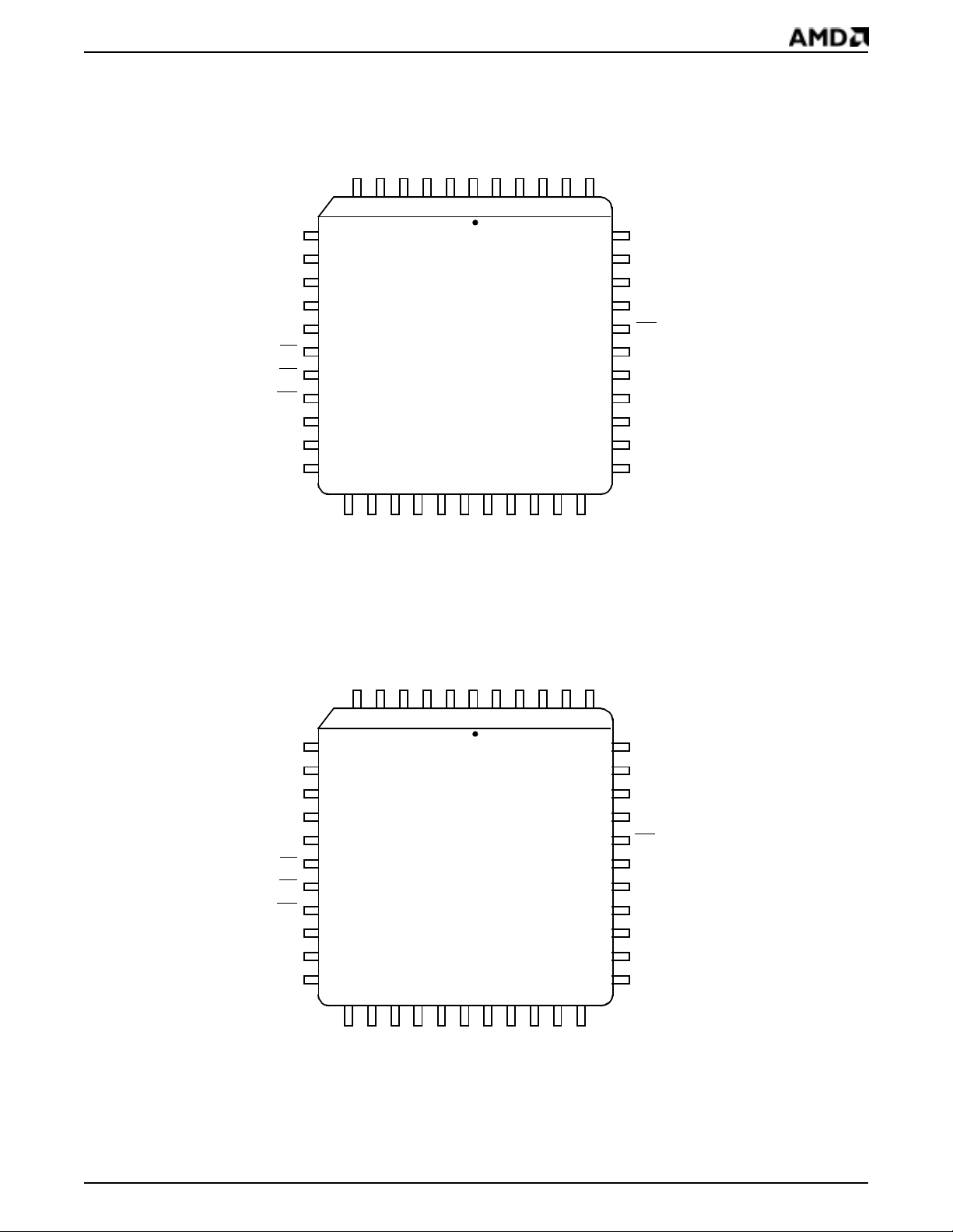
CONNECTION DIAGRAMS
Top View
CAP1
CAP2
AV
CC
DV
CC
RESET
CS
RD
WR
DV
SS
A2
A1
10
11
12
13
14
15
16
17
7
8
9
AVSSAINB
6
18
AINA
5
4
192021
44-Pin PLCC
EAR2
EAR1
LS2
3
2
1
Am79C30A
22
23
24
LS1
44
25
AREF
43
26
LIN1
42
27
LIN2
41
39
38
37
36
35
34
33
32
31
30
29
28
HSW
40
LOUT1
LOUT2
AV
SS
DV
SS
INT
XTAL 1
XTAL 2
MCLK
SFS
SCLK
SBOUT
RSRVD
RSRVD
AV
CC
DV
CC
RESET
CS
RD
WR
DV
SS
A2
A1
7
8
9
10
11
12
13
14
15
16
17
A0
D7D6D5
RSRVD
RSRVD
6
5
181920
44-Pin PLCC
RSRVD
RSRVD
4
3
Am79C32A
21
D4
22
BCL/CH2STRB
RSRVD
2
D3D2D1
LS2
1
23
24
LS1
44
25
AREF
43
26
LIN1
42
D0
27
LIN2
41
SBIN
28
HSW
40
39
38
37
36
35
34
33
32
31
30
29
LOUT1
LOUT2
AV
SS
DV
SS
INT
XTAL 1
XTAL 2
MCLK
SFS
SCLK
SBOUT
A0
D7D6D5
D4
D3D2D1
D0
SBIN
Note:
1. Pin 1 is marked for orientation purposes.
BCL/CH2STRB
2. RSRVD = Reserved pin; should not be connected externally to any signal or supply.
Am79C30A/32A Data Sheet 3
Page 4
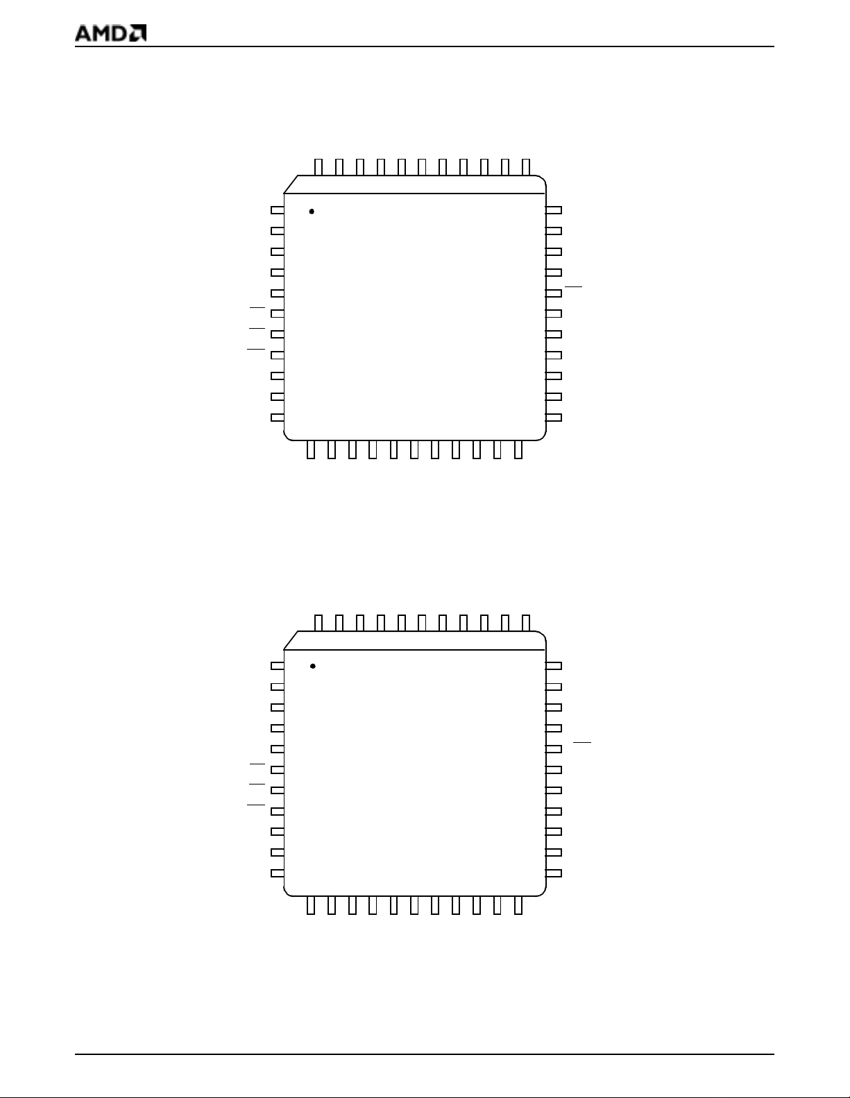
CONNECTION DIAGRAMS (continued)
Top View
AVSSAINB
AINA
44-Pin TQFP
EAR2
EAR1
LS2
LS1
AREF
LIN1
LIN2
HSW
CAP1
CAP2
AV
CC
DV
CC
RESET
CS
RD
WR
DV
SS
A2
A1
1
2
3
4
5
6
7
8
9
10
11
444342
12
131415
A0
D7D6D5
41
40
39
Am79C30A
16
17
D4
BCL/CH2STRB
44-Pin TQFP
38
37
18
19
20
D3D2D1
36
21
D0
35
34
LOUT1
33
LOUT2
32
AV
31
30
29
28
27
26
25
24
23
SS
DV
SS
INT
XTAL1
XTAL2
MCLK
SFS
SCLK
SBOUT
22
SBIN
RSRVD
RSRVD
AV
CC
DV
CC
RESET
CS
RD
WR
DV
SS
A2
10
A1
11
Note:
Pin 1 is marked f or ori entation purposes.
RSRVD
44
1
2
3
4
5
6
7
8
9
121314
A0
RSRVD
RSRVD
43
42
15
D7D6D5
RSRVD
RSRVD
41
40
Am79C32A
16
17
D4
BCL/CH2STRB
LS2
LS1
39
38
18
19
D3D2D1
RSRVD
LIN1
LIN2
HSW
37
36
35
34
20
21
33
32
31
30
29
28
27
26
25
24
23
22
LOUT1
LOUT2
AV
SS
DV
SS
INT
XTAL1
XTAL2
MCLK
SFS
SCLK
SBOUT
D0
SBIN
4 Am79C30A/32A Data Sheet
Page 5

ORDERING INFORMATION
Standard Products
AMD® standard products are available in several packages and operating ranges. The order number (Valid Combination) is
formed by a combination of the elements below.
AM79C30A/32A
JC
OPTIONAL PROCESSING
Blank = Standard Processing
TEMPERATURE RANGE
C = Commercial (0°C to +70°C)
PACKAGE TYPE
J = 44-Pin Plastic Leaded Chip Carrier (PL 044)
V = 44-Pin Thin Plastic Quad Flat Pack (PQT044)
SPEED OPTION
Not Applicable
DEVICE NAME/DESCRIPTION
Am79C30A/32A
Digital Subscriber Controller (DSC) device
ISDN Data Controller (IDC) device
V alid Combinations
AM79C30A JC, VC
AM79C32A JC, VC
Reference Appendix C, Figures 1 & 2, for specific mechanical dimensions of the two packages.
Valid Combina tions li st configu rations p lanned to be supported in volume for this device. Consult the loc al AMD sales
office t o conf irm av ai labi lity of specif ic valid combinations and
to check on newly released combinations.
Valid Combinations
Am79C30A/32A Data Sheet 5
Page 6

PIN DESCRIPTION*
Line Interface Unit (LIU)
HSW
Hook-Switch (Input)
The HSW signal indicates if the hook-switch is on or off
hook. This signal may be generated with a mechanical
switch wired to ground with a pu ll-up resistor to V
Any change in the HSW state causes an interrupt.
LIN1, LIN2
Subscri ber Li ne Input (Differential Inpu t s)
The LIN1 and LIN2 inputs interface to the subscriber (S
reference point) via an isolation transformer. LIN2 is the
positive inpu t; LIN1 is the ne gative input. Th ese pins
are not TTL compatible.
LOUT1, LOUT2
Subscriber Line Output (Differential Outputs)
The LOUT1 and LOUT2 line driver output signals interface to the subscriber line at the S reference point via
an isolation transformer and resistors. LOUT2 is the
positive S-interface driver (sources current during a
High mark), and LOUT 1 is the negative S-interface
driver (sources current during Low mark). For
multi-point applications, all TEs must maintain the
same po larity on t he S Interface. T hese pins are not
TTL compatible.
CC
Main A ud io Processor (MAP)
All MAP pins are analog, and therefore are not TTL
compatible.
AINA, AINB
Analog (Inputs)
These analog inputs allow for two separate analog (audio) inputs to the transmit path of the codec/filter.Input
signals on either of the se pins must be referenced to
AREF.
AREF
Analog Reference (Output)
This is a nominal 2.25-V reference voltage output for biasing the analog inputs. When the MAP is disabled,
this pin is high impedance.
CAP1, CAP2
Capacitor/Resistor (CAP1, Input; CAP2, Output)
An external resistor and capacitor are connected in series between thes e pins. These components are
needed for the integrator in the Analog-to-Digital Converter (ADC).
EAR1, EAR2
Earpiece Interface (Differential Outputs)
EAR1 and EAR2 are the outputs from the receive path
of the codec/filter. These differential outputs can directly drive a minimum load of 130 ohms.
LS1, LS2
Loudspeaker Interface (Differential Outputs)
.
LS1 and LS2 are push-pull outputs which can directly
drive a minimum load of 40 ohms.
Microprocessor Interface (MPI)
A2–A0
Address Line (Inputs)
A2, A1, and A0 signals select source and dest ination
registers for read and write operations on the data bus.
CS
Chip Select (Input)
must be Low to re ad or w rite to the Am 79C30A /
CS
32A. Data transfer occurs over the bidirectional data
lines (D7–D0).
D7–D0
Data Bus ( Bidi rect ional with High -I mpeda nce Stat e)
The eight bidire ctional data bus lines are used to exchange information with the microprocessor. D0 is the
least significant bit (LSB) and D7 is the most significant
bit (MSB). A High on the data bus line corresponds to
a logic 1, and Low corresponds to a logic 0. These lines
act as inputs when both WR and CS are active and as
outputs when both RD
inactive or both RD
pins are in a high-impedance state.
INT
Interrupt (Output)
An active Low output on the INT
nal microprocessor that the Am 79C30A /32A needs interrupt service. INT
INT
pin remains active until the Interrupt Reg ister (IR)
is read or the Am79C30A/32A is reset.
RESET
Reset (Input)
Reset is an active High signal which causes the
Am79C3 0A/32A to im mediate ly termin ate its prese nt
activity and initialize to the reset condition. When reset
returns Low, the Am79C30A/32A enters the Idle mode.
The MCLK output remains active while RESET is hel d
High.
and CS are active. When CS is
and WR are inactive, the D7–D 0
pin informs the exter-
is updated once every 125 µs. The
Note:
* All signal levels are TTL compatible unless otherwise stated.
6 Am79C30A/32A Data Sheet
Page 7

RD
Read (Input)
The active Low read signal is conditioned by CS
and indicates that internal information is to be transferred
onto the data bus. A num ber of interna l registers are
user accessible. The contents of the accessed register
are transferred onto the data bus after the High to Low
transition of the RD
input.
WR
Write (Input)
The active Low write signal is conditioned by CS
and
indicates that external information on the data bus is to
be transferred to an inter nal register. The contents of
the data bus are loaded on the Low t o High transition of
the WR
input.
Oscillator (OSC)
MCLK
Master Clock (Output)
The MCLK output is available for use as the system
clock for the microprocessor. MCLK is derived from the
12.288-MHz crystal via a programmable divider in the
Am79C30A/32A which provides the following MCLK
output frequencies: 12.288, 6.144, 4.096, 3.072, 1.536,
0.768, and 0.384 MHz.
XTAL1, XTAL2
External Crystal (Output, Input)
XT AL1 and XTAL2 are connected to an external parallel
resonant cr ystal for the on-chip oscillator. XTAL2 can
also be connect ed to an external source inste ad of a
crystal, in which case XTAL1 should be left disconnected. The frequency must be 12.288 MHz, ± 80 ppm.
Peripheral Port (PP)
SBIN
Serial Data (I np ut / Output)
When the Peripheral P ort is programmed to SBP mode,
SBIN operates as an input for serial data. When the Peripheral Por t is programm ed to IOM-2 mode, SBI N
functions as the data input except in the special case of
IOM-2 Slave mode, when it becomes an open-drain
output during pa rt or all of the IOM-2 fram e, or when
deactivated.
SBOUT
Serial Data (I np ut / Output)
When the Peripheral P ort is programmed to SBP mode,
SBOUT operates as an output for serial data. When the
Peripheral P ort is programmed to IOM-2 mode, SBOUT
functions as the data output except in the special case
of IOM-2 Slave mode when it becomes an input during
part or all of the IOM-2 frame.
SCLK
Serial Data Clock (Input/Output)
When the PP is prog r ammed to SBP mode, SCLK outputs a 192-k Hz data clock, wh ich may be inverted
under software control. When the PP is programmed to
IOM-2 Mast er m ode, SC LK o utputs a 1.536 -MHz 2X
data clock. In IOM- 2 Slave mode, SCLK functions as
the clock input. The SCLK pin defaults to a high-impedance st ate upon reset, bu t becom es active a fter any
MUX connection is made or if the PP is programmed to
IOM-2 Master mode.
SFS
Serial Fram e Syn c (Inp ut / Ou tp ut)
In SBP mode, SFS outputs an 8-kHz frame synchronization signal. SFS is an output in IOM-2 Master mode,
and an input in IOM -2 S lave mode. As an out put , S FS
is active for 8-bit periods. The SFS pin defaults to a
high-impedance state upon reset, but becomes active
after any MUX connection is made or if the PP is programmed to IOM-2 Master mode. For SBP mod e, the
active signal state is Low during Idle and 8 kH z in Active Data Only and Active Voice and Data modes.
BCL/CH2STRB
Bit Clock/SBP Channel 2 Strobe
(Output, Three-state)
In SBP mode, this pin provides a strobe during the 8-bit
times of the seco nd 64-kbit/s d ata channel. In IOM -2
Master mode, this pin provides a 768-kHz bit clock to
aid in the connection of non-IOM-2 devices to the port.
In IOM-2 Slave mode, this pin is high-impedance.
Power Supply Pins
PLCC/TQFP Packages
AV
CC
AV
SS
DV
SS
DV
CC
Note:
For best performance, decoupling capacitor s should be installed betw een V
Do not use separate supplies for analog and digital power
and ground connections.
+5-V analog power supply, ±5%
Analog ground
Di gital ground
+5-V digital power supply, ±5%
and VSS as close to the chip as pos sible.
CC
Am79C30A/32A Data Sheet 7
Page 8

OPERATIONAL DESCRIPTION
Overview of Power Modes
The minimization of power consumption is a key factor
in the design of Terminal Equipment for the ISDN, and
the DSC/IDC circuit employs two basic app roaches to
power management:
1. The power consumption of the DSC/IDC circuit itself is managed by using four basic power modes
which allow unu sed functional blocks to be disabled. The INIT register may be programmed to select Active V oice and Data, Active Data Only, Idle, or
Power-Down mode, depending upon which DSC/
IDC device resources are required at the time.
2. The power consumption of the controlling micro- processor system may be controlled by driving the processor clock with the DSC/IDC circuit MCLK output.
A wide ra nge of MCLK ope rating f requen cies ma y be
selected, and a special Clock Speed-Up function is
provided which increases the speed of MCLK upon
the occurrence of a key event, without processor intervention. Control of MCLK frequency and Clock
Speed-up i s acc om pl ished by pr ogramming t he I NI T
and INIT2 registers, as descri bed later.
Active Voice and Data Mode
In Active Voice and Data mode al l functional blocks of
the DSC/IDC circuit are available . Device registers may
be accessed through the MPI, the LIU and DLC are
available, t he OSC is ru nning, the Perip heral Por t is
available, MUX connections may be made, the Secondary Tone Ringer may be activated, and the MA P is
operational (DSC circuit only).
Active Data Only Mode
Active Data Only mode is similar to Active Voice and
Data mode, except that the MAP (DSC circuit only) is
disabled to reduce system power co nsumption. This increases the amount of power available f o r t he Secondary Tone Ringer or microprocessor system during the
phases of call setup and teardown, or during a
data-only telephone call.
Idle Mode
Idle mode is the RESET default mode of DSC/IDCcircuit operation, and rep resents an operational sta te in
which power consumption is reduced, yet the microprocessor system is operational to program DSC/IDC circuit registers or perform other required background
tasks. Idle mode may also be ente red by appropriate
programming of the INIT register.
In Idle mode, the MCLK output is available to drive the
microprocessor system, the MPI is available for programming of DSC /IDC registers, and the LIU is available to initiate or respond to S/T interface activity. The
HSW hookswit ch interrupt is als o avai lable in I dle mode.
Idle mode reduces DS C/IDC circ uit power cons umption by disabling the MUX, DLC, and MAP functional
blocks. The P eripheral Port is also disabled, except that
an IOM-2 activation request interr upt is possible, and
the SFS and SCLK outputs may still be activated. The
SFS and SCLK outputs are hig h impedanc e u pon RE SET, but bec ome active after any MUX connect ion is
programmed. The DLC read-only registers are cleared
when the DSC/IDC circuit enters the Idle mode.
Power-Down Mode
Power-Do wn mode consumes the least power of all the
DSC/IDC power options, and differs from Idle mode in
that all clocks, including the XTA L oscillator, are
stopped. Most functiona l blocks are disabled, except
for those required to recognize key external events that
will force the DSC/IDC circuit to return to Idle mode.
The Power-Down mode is not available unless the
Power-Down Enable bit is set in the INIT2 register; see
the INIT2 register description for further details.
Entering the Power-Down Mode
The Power-Down mode is entered by appropriate programming of the INIT and INIT2 registers. Selection of
the Power-Down mode cause s the DSC/IDCcircu it to
begin an internal countdown of at least 250 MCLK cycles after which the MCLK and XT AL1 outputs are both
stopped and held High, and the XTAL2input will be disregarded. The purpose of this countdown cycle is to
allow the microprocessor time for housekeeping operations before its clock is stopped. If an interrupt causes
the DSC INT pin to go Low during the countdown, the
Power-Do wn mode bits in the INIT register will be reset
and the countdown will be canceled.
If the LIU is enabled and in any state ot her than F3 at
the end of the countdown, MCLK is stopped but the oscillator con tinues to r un. T his al lows the LIU to identify
the incoming signal and either (1) generate an interrupt
and force the DSC/IDC circuit to Idle mode when activation is complete, or (2) move to the F3 state and stop
the oscillator once the line goes idle.
Exit i ng the Power-D own Mode
The DSC/IDC circuit will exit the Power-Down mode
and enter the Idle mode if any of the following events
occur:
• The DSC/IDC circuit receives a hardware reset via
the RESET pin.
•The CS
same ti me, as woul d occur du ring a n orma l writ e
operation from the microprocessor to the DSC circuit. No data will be transferred by this operation.
• The HSW hookswitch pin changes state, and the
hookswitch interrupt is enabled.
and WR pins a re both pulled Low at the
8 Am79C30A/32A Data Sheet
Page 9

• The LIU receiver is enabled, detects an incoming
signal on the S/T Interface, and achieves activation
as indicated by a transition to state F7. Both the INT
pin and the F7 t ransition interrupt must b e enabled
for Power-Down mode to be exited. If the LIU is enabled, it may restart the oscillator so that it can identify the activity on the interface. If the activity is
determined to be noise, the LIU will stop the oscillator and continue to monitor the line without an interrupt or returning to Idle mode.
• The IOM-2 Interface is enabled as a clock master
and the SBIN input pin goes Low . This indicates that
a slave device wants to activate the IOM-2 Interface
and communicate with the DSC circuit. Both the INT
pin and the IOM-2 timing request interrupts must be
enabled for Power-Down mode to be exited.
• The IOM-2 Interface is enabled as a clock slav e and
the SCLK input pin goes High. This indicates that
the master device is activating the IOM-2 Interface
and the DSC circuit must wake up in order to monitor the data. Both the INT
pin and the IOM-2 timing
request interrupts must be enabled for Power-Down
mode to be exited.
If the DSC/IDC circuit is awakened by any condition
other than RESET, the MCLK output will be r estored to
its previously programmed frequency, and will not generate any shortened or spurious output cycles. If the
DSC/IDC circu it is revi ved by RESET, MCLK will defau lt
to its normal 6.144-MHz rate. The DSC/IDC circuit provides a minimum of two MCLK cycles prior to activating
the interrupt pin when exiting Power-Down mode.
MCLK Frequency Control
The MCLK frequency selection bits in the INIT register
are unchanged from Revision D. However, additional
MCLK frequencies are available by programming bits in
the INIT2 reg ister. No shor tened or spur ious clock
pulses that might disru pt the external microprocessor
will result when the MCLK frequency is changed.
In order to reduce the probability of errant software disruptin g system op eration, th e INIT2 reg ister require s
two consecutive writes before the value will be entered
into the register. Note that there will be no MCLK countdown as is the c ase for entering Power-Down mode if
INIT2 is programmed to cause MCLK to STOP, and
there will be no shortened or spurious MCLK pulses.
MCLK Clock Speed-up Function
A programmable aut omatic MCL K speed-up option is
provided that will force a hardware reset of INIT2 bit s
3-0, which will cause the MCLK frequency to be restored to the value programmed in the INIT register.
There are two events that will trigger the clock
speed-up function:
1. The DLC receive FIFO threshold has been reached;
or,
2. a second packet begins to be recei ved while data
from a prior pa cket is still in th e rece i ve FIF O.
The second packet case requires provision of an interrupt; see the DLC regi ster section for further information. The clock speed-up function allows the user to
program a ver y slow MCLK frequ ency using INI T2
when D-channel activity is minimal. If a burst of activity
is seen on the D channel and it exceeds the programmed threshold of the receive FIFO or threatens to
overrun the rece ive FIFO s tatus buffers, MCL K will instantly toggle back to the higher frequency programmed in the INIT register. This eliminates the
latency incurred if an interrupt has to be serviced to
change the clock speed, and allows the overall system
power to be reduced during typical voice connec tions.
Note that automatic clock speed-up will not function unless at least one of the associated interrupts are enabled so the processor can be informed that the c lock
speed has been altered.
Global Register Functions
INIT Register (INIT) default = 0 0H
Address = Indirect 21 Hex, Read/Write
Table 1. INIT Register
Bit
Function76 5 43210
XXXXXX00Idle mode
X X X X X X 0 1 Active Voice and Data mode
X X X X X X 1 0 Active Data Only mode
X X X X X X 1 1 Power-Down m ode
XXXXX0XXINT
XXXXX1XXINT
X X 0 0 0 X X X MCLK frequency = 6.144 MHz
X X 0 0 1 X X X MCLK frequ ency = 12.288 MHz
X X 0 1 0 X X X MCLK frequency = 3,072 MHz
X X 0 1 1 X X X MCLK frequency = 6.144 MHz
X X 1 0 0 X X X MCLK frequency = 4.096 MHz
X X 1 0 1 X X X MCLK frequency = 6.144 MHz
X X 1 1 0 X X X MCLK frequency = 6.144 MHz
X X 1 1 1 X X X MCLK frequency = 6.144 MHz
X 0 X X X X X X DLC receiver abort disabled
X 1 X X X X X X DLC receiver abort enabled
0 X X X X X X X DLC transmitter abort disabled
1 X X X X X X X DLC transmitter abort enabled
output enabled
output disabled
Am79C30A/32A Data Sheet 9
Page 10

INIT2 Register (INIT2) default = 00 H
Address = Indirect 20 Hex, Read/Write
A special write procedure must be followed in order to
modify the contents of the INIT2 Register, since the
INIT2 Register includes control bits which coul d result
in the stopping of the microprocessor clock. This procedure greatly reduces the probability of errant software
disabling the system, and is described as follows:
1. Write the INIT2 address to the Command Register.
2. Write to the Data Register (INIT2 is not yet updated).
3. Write the INIT2 address to the Command Register.
4. Write to the Data Register (INIT2 is updated).
The writes must take place without any intervening indirect accesses to the DSC/IDC circui t.
Table 2. I NIT2 Register
Bit
7 6 5 4 3 2 1 0 Function
00XXXXXXReserved, must be written to 0;
READs are undefined
0 0 0 X X X X X Power-Down disabled; writing
11 to the INIT Register will put
the DSC/IDC circuit into Idle
mode
0 0 1 X X X X X Power-Down enabled; writing
11 to the INIT Register will put
the DSC/IDC circuit into
Power-Down mode
0 0 X 0 X X X X Multiframe Interrupt filter
disabled
0 0 X 1 X X X X Multiframe Interrupt filter
enabled (see LIU sect ion for
detailed descripti on)
0 0 X X X 0 X X Clock speed- up option disab led
0 0 X X X 1 X X Clock speed- up option enab led;
if set, this register bit will be
cleared when the DLC FIFO
receive thr eshold or second
packet received interrupt is
triggered
0 0 X X X 0 0 0 MCLK frequenc y determined by
INIT Register
0 0 X X X 0 0 1 MCLK frequency is 1.536 MHz
0 0 X X X 0 1 0 MCLK frequency is 768 kHz
0 0 X X X 0 1 1 MCLK frequency is 384 kHz
0 0 X X X 1 0 0 MCLK stopped in High state
0 0 X X X 1 0 1 Reserved
0 0 X X X 1 1 0 Reserved
0 0 X X X 1 1 1 Reserved
RESET Operation
The Am79C3 0A/32A can be reset by dr iving the
RESET pin High. When power is first supplied to the
DSC/IDC circuit, a reset must be performed. This initializes the DSC /IDC circuit to its default con dition as
defined in Table 3.
Table 3. Reset Pin Conditions
Pin Name State Following RESET
D7–D0 High Impedance
MCLK 6.144 MHz
INT Logical 1
SBOUT High Impedance
SFS High Impedance
SCLK High Impedance
LS1, LS2 High Impedance
EAR1 High Impedance
EAR2 High Impedance
AREF High Impedance
LOUT1 High Impedance
LOUT2 High Impedance
Receive and Transmit Abort Commands
The microprocessor has the option via INIT Register
bits 6 and 7 to abort the receive and transmit D-channel
packets. When the micro processor sets one of these
bits, the Am79C30A /32A a bort s the respective operation. Th e frame ab ort se quence is d efined in gre ater
detail l ater. (See th e Data Lin k Contro ller sec tion on
page 36.)
Interrupt Handling
The Am79 C30A/32A generates either no inte rrupt or
only one interrupt ev ery 125 µs. Once asserted, INT
mains active unt il the microproc essor responds by interrogating the Am 79C30A/32A ’s Interrupt Register (IR)
(see Table 4). Read ing the IR in re sponse to an activated INT
pin deactivates the INT p in and clears the IR.
If an event causing an interrupt occurs while the IR is
being read by the microprocessor, the effect of the
event is held until the microprocessor has completed its
read cycle. A reset clears all conditions causing interrupts.
Bits 0, 1, and 4 of the IR, if set, advise the microprocessor that the respective buffer is ready for reading or
writing. If bit 0 is set due to an empty buffer , the D-channel T r ansmit buffer must be serviced within 375 µs. If bit
1 is set an d the D-ch annel Re ceive buffer is fu ll, the
buffer must be serviced within 425 µs. This is to prevent
erroneous data transfers causing transmitter underrun
and receiver overrun errors. If bit 4 is set then the Bb or
re-
10 Am79C30A/32A Data Sheet
Page 11

Bc buffers must be accessed within 122.4 µs. This is to
prevent erroneous data transfers. Only one interrupt is
used to signal accessibility for both B channels of the S
Interface. Since the data transfer must occur synchronously to the S Interface, any data access to either Bb
or Bc or both must be made within the122.4 µs limit.
Note that even though only a single interrupt is issued,
either or both S-Interface B channels must be serviced.
IR bits 2, 3, 5, 6, and 7, if set, indicate that a bi t has
been set in the associated status or error register. All of
the interrupts generated by the Am79C30A/32A can be
individually disabled. In the case of IR bit 7, the interrupt can also be masked by setting PPIER bit 7 to 0.
DMR1, DMR2, DMR3, LMR2, MCR4, and MF control
the mask conditions that affect the INT
pin. The INT pin
is activated only by interrupts that are not disabled. The
Interrupt Register refle cts the status of enabled interrupt s . Th e I NT
pin can be disabled by setting INIT Reg-
ister bit 2 to a logical 1.
The Am79C30A/32A has facilities that allow the micro-
processor to read the status registers (status update is
inhibited during status read) or the IR at any time during functional operation.
Am79C30A/32A Data Sheet 11
Page 12

Table 4. Format of the Interrupt Register (IR), Read Only
Bit Interrupt Generated/Action Requir ed Interrupt Mask
0 D-channel tr ansm it threshold interrupt/load D-chann el Transmit b uffer DMR1 bit 0
1 D-channel recei ve threshold int errupt/read D-channel Receive buf fer DMR1 bit 1
2 D-channel status interrupt/read DSR1
Source Cause
DSR1 bit 0 Valid Address (VA) or End of Address (EOA) DMR3 bit 0
DSR1 bit 1 When a closing flag is receiv ed or a receive error oc curs DMR1 bit 3
DSR1 bit 6 When a closing flag is transmitted DMR3 bit 1 DMR3 bit 1
3 D-channel error in terrupt/read DER and DSR2 bit 2
Source Cause
DER bit 0 Current received packe t has been aborted DMR2 bit 0
DER bit 1 Non-integer number of bytes received DMR2 bit 1
DER bit 2 Collision abort detected DMR2 bit 2
DER bit 3 FCS error DMR2 bit 3
DER bit 4 Overflo w err or DMR2 bit 4
DER bit 5 Underflow error DMR2 bit 5
DER bit 6 Overrun error DMR2 bit 6
DER bit 7 Underrun error DMR2 bit 7
DSR2 bit 2 Receive packet lost DMR3 bit 6
4 Bb or Bc byte available or buffer empty interrupt/read or write Bb or Bc buffers MCR4 bit 3
5 LIU status interrupt/read LSR
Source Cause
LSR bit 3 Change of state to F3 LMR2 bit 3
LSR bit 4 Change of state fr om /t o F7 LMR2 bit 6
LSR bit 5 Change of state fr om /t o F8 LMR2 bit 4
LSR bit 7 HSW change of state LMR2 bit 5
6 D-channel status interrupt/read DSR2
Source Cause
DSR2 bit 0 Last byte of received pac ket DMR3 bit 2
DSR2 bit 1 Receive byte av ailable DMR3 bit 3
DSR2 bit 3 Last byte transmitted DMR3 bit 4
DSR2 bit 4 T ransmit buffer available DMR3 bit 5
DSR2 bit 7 Start of second packet EFCR bit 1
7 Multiframe or PP interrupt/read MFSB and PPSR
Source Cause
MFSB bit 5 S-data av ailable MF bit 1
MFSB bit 6 Q-bit buffer empty MF bit 2
MFSB bit 7 Multiframe change of state (in/out of sync) MF bit 3
PPSR bit 0 Monitor receive, data available PPIER bit 0
PPSR bit 1 Monitor transmi t, buffer available PPIER bit 1
PPSR bit 2 Monitor EOM receive d PPIER bit 2
PPSR bit 3 Monitor abort received PPI ER bit 3
PPSR bit 4 C/I channel 0, data change PPIER bit 4
PPSR bit 5 C/I channel 1, data change PPIER bit 5
PPSR bit 6 IOM-2 timing request PPIER bit 6
12 Am79C30A/32A Data Sheet
Page 13

FUNCTIONAL DESCRIPTION
Microprocessor Interface (MPI)
The Am79C30A/32A can be connected to any general
purpose 8-bit microproces sor via the MPI. The MCLK
from the Am79C30A/32A can be used as the clock for
the microprocessor. The MPI is an interrupt-driven interface containing all the circuitry necessary for access
to th e inter nal pr ogramm able re gister s, statu s regi sters, coefficient RAM, and transmit/receive buffers .
MPI External Interface
External connections to the MPI are shown in Tab le 5.
Table 5. MPI External Interface
Name Direction Function
D7–D0 Bidirectional Data Bus
A2–A0 Inputs Address Line
RD Input Read Enable
WR Input Write Enable
CS Input Chip Select
RESET Input Initialization
INT Output Interrupt
Direct Registers
Access to the Direct Registers of the Am79C30A/32A
is controlled by the st ate of the CS
, RD, WR, A2, A1,
and A0 input pins, as defined below by Table 6.
Indirect Registers
To read from or write to any of the Indirect Registers, an
indirect address command is first written to the Command Register (CR). One or more data bytes may then
be transferred to or from the selected register through
the Data Register (DR).
Registers within certain groups can be accessed
quickly by using internal circuitry which automatically
increments the indirect value. In Table 7, the bytes
transferred numbers are the number of bytes which are
read or written to the DR after the CR has been loaded.
Whenever the CR is loaded, any previous commands
are automatically terminated.
Table 6. Direct Register Access Guide
CS RD WR A2 A1 A0 Register(s) Accessed Mode
010000Command Register (CR) W
001000Interrupt Register (IR) R
010001Data Register (DR) W
001001Data Register (DR) R
001010D-channel Status Regist er 1 (DSR1) R
001011D-channel Error Register (DER) (2-byte FIFO) R
010100D-channel Transmit buff er (DCTB) (8- or 16-byte FIFO) W
001100D-channel Receive buffer (DCRB) (8- or 32-byte FIFO) R
010101Bb-channel Transmit buff er (BBTB) W
001101Bb-channel Receive buffer (BBRB) R
010110Bc-channel Transmit buffer (BCTB) W
001110Bc-channel Receive buffer (BCRB) R
001111D-channel Status Regist er 2 (DSR2) R
1 X X X X X No access (X = logical 0 or 1) —
Note:
The RD
and WR signals must never both be Low under normal operating conditions.
Am79C30A/32A Data Sheet 13
Page 14

Tabl e 7. Indirect Register Access Guide
Operation
Block Register
INIT Initialization Regist er 1 INIT R/W 21H One byte trans ferred
INIT Initiali zation Register 2 2 INIT2 R/W 20H One byte transferred
LIU LIU Stat us Register 1 LSR R A1H One byte transferred
LIU LIU Priorit y Regi ster 2 LPR R/W A2H One byte tr ansferred
LIU LIU Mode Register 1 3 LMR1 R/W A3H One byte transferred
LIU LIU Mode Register 2 4 LMR2 R/W A4H One byte trans ferred
LIU — 5 Perform 2–4 – A5H
LIU Multiframe Register 6 MF R/W A6H One byte tr ansferred
LIU Multiframe S-bit/Status Register 7 MFSB R A7H One byte transferred
LIU Multiframe Q-bit buffer 8 MFQB W A8H One byte transferred
MUX MUX Control Register 1 1 MCR1 R/W 41H One byte transferr ed
MUX MUX Control Register 2 2 MCR2 R/W 42H One byte transferr ed
MUX MUX Control Register 3 3 MCR3 R/W 43H One byte transferr ed
MUX MUX Control Register 4 4 MCR4 R/W 44H One byte transferr ed
MUX — 5 Pe rform 1–4 — 45H MCR1, 2, 3, 4
MAP X filter Coefficient Register 1 X Coeff. R/W 61H h0 LSB, h0 MSB...h7 MSB
MAP R filter Coefficient Register 2 R Coeff. R/W 62H h0 LSB, h0 MSB...h7 MSB
MAP GX Gain Coefficient Register 3 GX Coeff. R/W 63H LSB, MSB
MAP GR Gain Coefficient Register 4 GR Coeff. R/W 64H LSB, MSB
MAP GER Gain Coefficient Register 5 GER Coeff. R/W 65H LSB, MSB
MAP Sidetone Gain Coefficient Register 6 STG Coeff. R/W 66H LSB, MSB
MAP Frequency T one Generator Regi ster
1, 2
MAP Amplitude Tone Generator Regist er
1, 2
MAP MAP Mode Register 1 9 MMR1 R/W 69H One byte transferred
MAP MAP Mode Register 2 10 MMR2 R/W 6AH One byte transferred
MAP — 11 Perform 1–10 — 6BH 46 bytes loaded 1–10
MAP MAP Mode Register 3 12 MMR3 R/W 6CH One byte transferred
MAP Secondary T one Ringer Amplitude 13 STRA R/W 6DH One byte transferred
MAP Secondary To ne Ringer Frequency 14 STRF R/W 6EH One byte transferred
MAP Tr ansmit Peak Regist er 15 PEAKX R 70H One byte transf erred
MAP Receive Peak Regist er 16 PEAKR R 71H One byte transferred
MAP — 17 Perform 15–16 R 72H One byte transf erred
DLC First Received Byte Address
Registers 1, 2, 3
DLC Second Received Byte Address
Registers 1, 2, 3
DLC Transmit Address Register 3 TAR R/W 83H LSB, MSB
DLC D-channel Receive Byte Limit
Register
DLC D-channel Transmit Byte Count
Register
Register
Number Indirect Name Mode Address Byte Sequence
One byte transferred
7 FTGR1, FTGR2 R/W 67H FTGR1, 2
8 ATGR1,ATGR2 R/W 68H ATGR1, 2
1 FRAR 1, 2, 3 R/W 81H FRAR1, 2
2 SRAR1, 2, 3 R/W 82H SRAR1, 2
4 DRLR R/W 84H LSB, MSB
5 DTCR R/W 85H LSB, MSB
14 Am79C30A/32A Data Sheet
Page 15
Table 7. Indirect Register Access Guide (Continued)
Operation
Block Register
DLC D-channel Mode Register 1 6 DMR1 R/W 86H One byte transferred
DLC D-channel Mode Register 2 7 DMR2 R/W 87H One byte transferred
DLC — 8 Perform 1–7 — 88H 4 bytes loaded 1–7
DLC D-channel Receive Byte Count
Register
DLC Random Number Generator
Register
DLC Random Number Generator
Register
DLC First Received Byte Address
Regi ster 4
DLC Second Received Byte Address
Regi ster 4
DLC D-channel Mode Register 3 14 DMR3 R/W 8EH One byte transferred
DLC D-channel Mode Register 4 15 DMR4 R/W 8FH One byte transferred
DLC — 16 Perform 12–15 — 90H FRAR4, SRAR4, DMR3,
DLC Address Status Register 17 ASR R 91H One byte transferred
DLC Extended FIFO Control Register 18 EFCR R/W 92H One byte transfe rred
PP Peri pheral P ort Control Register 1 1 PPCR1 R/W C0H One byte transferred
PP Peri pheral P ort Status Regi ster 2 PPSR R C1H One byte transferred
PP Peripheral Port Interrupt Enable
Register
PP Monitor Transmit Data Register 4 MTDR W C3H One byte transferred
PP Monitor Receive Data Register 5 MRDR R C3H One byte transferred
PP C/I Transmit Data Register 0 6 CITDR0 W C4H One byte tr ansferred
PP C/I Receive Data Regi st er 0 7 CIRDR0 R C4H One byte transferred
PP C/I Transmit Data Register 1 8 CITDR1 W C5H One byte tr ansferred
PP C/I Receive Data Regi st er 1 9 CIRDR1 R C5H One byte transferred
PP Peri pheral P ort Control Register 2 10 PPCR2 R/W C8H One byte transferr ed
PP Peri pheral P ort Control Register 3 11 PPCR3 R/W C9H One byte transferr ed
Register
Number Indirect Name Mode Address Byte Sequence
9 DRCR R 89H LSB, MSB
10 RNGR1 (LSB) R/W 8AH One byte transferred
11 RNGR2 (MSB) R/W 8BH One byte tr ansferred
12 FRAR4 R/W 8CH One byte transferred
13 SRAR4 R/W 8DH One byte transfe rr ed
DMR4
3 PPIER R/W C2H One byte transferr ed
Line Interface Unit (LIU)
The LIU connects to the four-wire S Interface through a
pair of isolation transformers, one for the transmit and
one for the receive direction, as shown in Figure 1.
The receiver section of the LIU consists of a differential
receiver, circuitry f or bit timing recov ery, circuitry for detecting High and Low marks, and a frame recovery circuit for frame sy nchronizat ion. The re ceiver converts
the received pseudo-ternary coded signals to binary
before delivering them to the other blocks of the
Am79C30A/32A. It also performs collision detection (Eand D-bit comparison) per the CCITT recommenda-
Am79C30A/32A Data Sheet 15
tions so several TEs can be connected to the same S
Inter face .
The transmitter consists of a binar y to pseudo-t ernar y
encoder and a differential line dr iver which meets the
CCITT recommendations for the S Interface.
The Am79C30A/32A can establish multiframe synchronization, receive S bits, and transmit Q bits synchronized to the received frame.
External Interface
The LIU can be connecte d to both point-to- point and
point-to-multipoint configurations at the CCITT S reference point. The point-to-point configuration consists of
one TE connected to the NT or PABX linecard. The
Page 16

point-to-multipoint configuration can have multiple TEs
connected to one NT.
Line Code
Pseudo-ternary coding is used for both transmitting
and receiving over the S Interface. In this type of coding, a binary 1 is represented by a space (zero voltage),
and a binary 0 is represented by a High mark or a Low
mark. T wo consecutive binary 0s are represented by alternate marks to reduce DC of fset on the line. A mark
followed, either im mediately or separated by spaces,
by a mark of the same polarity , is defined as a code violation. Code violations are used to identify the boundaries of the frame.
Note:
The DSC defines “Any Signal” as any frame with at least
three marks above receive threshold.
Frame Structures
In both transmit and receive directions, the bits are
grouped into frames of 48 bits each. The frame structure is identical for both point-to-point and point-to-multipoint configurations. Each frame transmitted at 4 kHz
consists of several groups of bits.
Multifram i ng
If multiframing is enabled, the A m79C30A/32A recognizes and establishes multiframe synchronization
based on the monitoring of the F
(Q-bit control) and M
A
(M-bit control) bits. The Am79C30A/32A also receives
and compiles S bits, and transmits Q bits synchronized
to the received frame.
Establishment of Multi fr am e Sy nc hroni z at io n
When the enable multiframe synchroni zation bit (bit 0
of the Multiframe Register) is set and the LIU is in either
state F6 or F7, the LIU monitors the F
(Q-bit control)
A
and M (M-bit control) bits. When three consecutive multiframes with the M bits and F
bits set as defined in
A
Table 8 are recei ved, the multiframe synchron ized bit
(bit 7 of the Multiframe Register) and multiframe
change of state bit (bit 7 of t he Mul tiframe S bi t/Status
buffer) are set. Note that S-bit data is received, compiled, an d transferre d to the use r after att aining s ynchronization at the start of the next multiframe.
S-Bit Reception
The default operation of the DSC/IDC circuit is that the
LIU will receive and pass multiframe data to the user in
5-bit increments four times per multiframe, regardless
of the value of the data. After multiframe synchronization has been requested and established the microprocessor can read the Multiframe S bit/Status buffer
(MFSB) once the S-bit available bit (MFSB bit 5) is set.
The S-data available bit is set to a logical 1 when the
Am79C30A/32A has received five S bits (one S bit per
S-interface frame) synchronized to the setting of the
F
-bit to a logical 1 and transferred them into the
A
MFSB. Once the S-bit available bit is set, the MFSB
must be accessed within 1.25 ms or succeeding S data
will be lost.
Subsequent to the original definition of the DSC/IDC
circuit, the CCITT has defined a structure for the 20
multiframe bits, which specifies five 4-bit channels. Furthermore, the idle code for these channels has been
defined as 0000. An enh anc ed m ode o f mult iframe reception has been included, which may be enabled by
setting INIT2 bit 4 to a 1. This enhanced mode reduces
processor overhead by generating an interrupt only
upon the reception of a non-zero S-channel word.
INIT2 bit 4 wil l be automatic ally cleared by ha rdware
when the five received data bits in the MFSB are not all
0s, as long as MF bit 1 (interrupt enable) is set. This allows subsequent valid all-zero words to be received.
Furthermore, when the first five S bits of the multiframe
are loaded into the MFSB, bit 4 o f the MF regist er will
be set, which allows identification of th e position of received words wit h in t h e mu lt iframe.
Binary
to
Pseudo-ternar y
To
MUX
Frame
Recovery
Coder
and
DLC
Decoder Slicer
Timing
Recovery
Figure 1. LIU Block Diagram
16 Am79C30A/32A Data Sheet
Line Drivers
S
Balanced
Receiver
09893H-2
Page 17

Table 8. Multiframin g Structu res
Frame Number NT-to-TE Q Control Bit FA NT-to-TE M Bit (M) NT-to-TE S Bit (S) TE-to-NT FA Bit (Q Bit)
1 1 1 SC11 Q1
2 0 0 SC21 0
3 0 0 SC31 0
4 0 0 SC41 0
5 0 0 SC51 0
6 1 0 SC12 Q2
7 0 0 SC22 0
8 0 0 SC32 0
9 0 0 SC42 0
10 0 0 SC52 0
11 1 0 SC13 Q3
12 0 0 SC23 0
13 0 0 SC33 0
14 0 0 SC43 0
15 0 0 SC53 0
16 1 0 SC14 Q4
17 0 0 SC24 0
18 0 0 SC34 0
19 0 0 SC44 0
20 0 0 SC54 0
1 1 1 SC11 Q1
2 0 0 SC21 0
etc.
Transmission of Q bits
The microprocessor can load the Multiframe Q-bit
buffer (MFQB) once the Q-bit buffer empty bit (bit 6 of
the Multiframe S bit/Status buffer) is set. The Q-bit
buffer empty bit is set to a logical 1 at reset or when
data that has been written to the Multiframe Q-bit buffer
is transferred to the L IU. The Q-bit buffer empty bit is
cleared to a logical 0 when the Mul tiframe S-bi t/Status
buffer is read. After multiframing has be en requested
and established, the Am79C30A/32A transfers the data
written into the Q-bit Register to the LIU, synchronized
to the multiframe, irrespective of the receipt of valid
Q-control bits. If the microprocess or does not reload
the Q-bit Register for retransmissions , the Q-bit pattern
is repeated in the next multiframe.
If multiframing is enabled but multiframe synchronization is not established, the LIU transmits the value
loaded in MFQB bit 4 in all Q bits. The default value of
MFQB bit 4 is a logical 0 which satisfies the CCITT recommendations. When synchronization is achieved, the
contents of MFQB bits 3 to 0 are transmitted according
to Table 8.
Loss of Multi fr a m e Synchronizatio n
The Am79C30A/32A continuously monitors the FA
(Q-bit control) and the M bits to ensure multiframe synchronization. Onc e multiframe synchronization is established, multiframe synchronization is lost if three
consecutive invalid multiframes are received, or the LIU
is no longer in state F6 or F7, or multiframing is disabled. When loss of multiframe synchronization occurs,
bit 7 of the Multiframe Register is set to a logical 0, and
bit 7 of th e Multifra me S bit/S tatus buffer is set to a
logical 1. The A m79C30A/ 32A also t erm inates the reception of S bits and transmission of Q bits until multiframing synchronization is re-established.
HSW
The hookswitch c ircuitry on the DSC circui t provides the
attached mic roprocessor with a way of converting an
external mechanical hookswitch into a software status
condition capabl e of generating an interrupt . De bounce
and glitch rejection are pr ov ided internal to the D SC circuit. The logic rej ects glitches less than 16 2 ns and provides deboun ce of 16 m s. HSW status repor ting is
disabled afte r RESET. It is enabled by any of the fo llo wing: taking the devic e out of Idl e mode , a write to a MUX
Control Register (MCR3–MCR1), or unmasking the
HSW interrupt.
Am79C30A/32A Data Sheet 17
Page 18

LIU Registers
The LIU contains the registers shown in Tab l e 9.
as 1, F4 as 2, and so on, where bit 0 is the LSB. The
LIU interrupts the microprocessor via bit 4 of the LSR
when activation has been achieved (that is, when the
LIU moves to state F7 upon receipt of INFO 4). During
T able 9. LIU Registers
Registers No./Registers Mnemonic
LIU Status Register 1 LSR
LIU Priority Register 1 LPR
LIU Mode Registers 2 LMR1, LMR2
Multiframe Register 1 MF
Multiframe S-bit/Status
Register
Multiframe Q-bit buffer 1 MFQB
1 MFSB
reset the LSR is 0.
Even though the LIU Status Register (LSR) is
read-only, no default value upon power-up is given due
to the uncer tain s tate of bit 6 (Hookswitch State). Following RESET, the LIU State is F2 and the HSW bit reflects the HSW pin, producing a power-up value of
either 00H or 40H.
LIU D-Channel Priority Register (LPR), Read/Write
The LPR cont ains the prio rity level for D-channel access. Its default value after reset is 0.
LIU Status Register (LSR), Read Only
Address = Indirect A1H
The LSR format is shown in Table 10.
Table 10. LIU Status Register
Generates
Bit Logical 1
0-2 Binary values 000 through 110
represent the LIU activation
circuitry’s current state (F2
through F8, respe ctively) bi t 2 is
MSB
3 Change of st ate to F3 If LMR2 bit 3 = 1
4 Change of st ate from/to F7 If LMR2 bit 6 = 1
5 Change of st ate from/to F8 If LMR2 bit 4 = 1
6 HSW state No
7 HSW change of state If LMR2 bit 5 = 1
Interrupt
No
When the microprocessor reads the LSR, bits 3, 4, 5,
and 7 are cleared. The other bits retain the current status of the LIU. bi ts 0 to 2 are defined such that state F2
(see CCITT I.430 state matrix tables) is coded as 0, F3
The D-channel access procedure of the Am79C30A/
32A uses the priority level programmed in the LPR. The
priority mechanism defined by the CC ITT I-series recommendations i s fully implem ented if the LPR is programmed via the m icroprocessor to con form to the
priority class of the Layer-2 frame to be transmitted.The
LPR has 16 possible programmable priority levels. The
priority levels are numbered 0–15. Priority Level 0 corresponds to counting eight 1s in the echo channel, priority Level 1 corresponds to counting ten 1s in the echo
channel, priority Level 2 corresponds to counting
twelve 1s, etc. The DSC circuit automatically handles
transitions between the programmed priority level n
and the associated odd value n + 1. Th e priority is
incremented following a succ essfully transmitted
packet, and decrem ented when the highe r count has
been satisfied.
The LPR format is shown in Table 11.
Table 11. LIU Priority Register
Bits Description
3, 2, 1, 0 D-channel access priority level bit 0 is LSB
7, 6, 5, 4 Reserved, reads logical 0
18 Am79C30A/32A Data Sheet
Page 19

LIU Mode Re gi st er ( LM R 1 ), Read/Write
Address = Indirect A3H
LMR1 is defined in Table 12.
Table 12. LIU Mode Register 1
Bit Logical 1 Logical 0 (default value)
0 Enable B1 tr ansmit Disable B1 transmit
1 Enable B2 tr ansmit Disable B2 transmit
2 Disable F tra nsm it Enable F transmit
3 Disable F
4 Activation request No activation request
5 Go from F8 to F3 No transition
6 Enable receiver/transmitter Disable receiver/transmitter
7 Reserved; must be set to logical 0 Reserved; must be set to logical 0
Notes:
The F a nd F
bits in LMR1 (bits 2 and 3) shou ld be enab led duri ng the acti va tion pr ocedu re so the Am79C30 A/32 A can respond
A
with INFO 3.
LMR1 bit 4 is used to tran sf er t he signal s PH-AR and Exp iry of Timer from t he micropr ocessor to the LIU (s ee CCITT I.4 30 state
diagram—activati on request). PH-AR i s defined as bit 4 being a logical 1 and Expiry of Timer is defined as the transition of bit 4
from a logical 1 to a logi cal 0. This bit must not be set until the LIU, as ref lected in the LSR, is in stat e F3, F6, or F7 and the
receiver has been enabled for a minimum of 250 µs.
LMR1 bit 6 is primarily used to disab le the r eceiv er when the terminal does not requi re access t o the S Inter f ace si gnals . This bi t
is cleared by reset and must be written to lo gical 1 in order to receive activati on from the S Interf ace, or to request acti vation.
transmit Enable FA transmi t
A
LIU Mode Register 2 (LMR2), Read/Write
Address = Indirect A4H
LMR2 is used to select the operations found in Table 13.
Table 13. LIU Mode Register 2
Bit Logical 1 Logical 0 (Default Value)
0 D-channel loopback at Am79C30A/32A enable D-channel loopback at Am79C30A/32A disable
1 D-channel loopback at LIU enable D-channel loopback at LIU disable
2 D-channel back-off disable D-channel back- off enable
3 F3 change of state i nterrupt enable F3 change of state interrupt disable
4 F8 change of state i nterrupt enable F8 change of state interrupt disable
5 HSW interrupt enable HSW interrupt disable
6 F7 change of state i nterrupt enable F7 change of state interrupt disable
7 Reserved; must be set to logical 0 Reserved; must be set to logical 0
Am79C30A/32A Data Sheet 19
Page 20

The three D-channel loopback controls defined in
Am79C30A NT/PABX
D
D
MPI
S
Am79C30A NT/PABX
DD
E
E
S
LMR2 bits 0, 1, and 2 are explained below:
Bit 0, D-channel loopback at Am79C30A/32A enable:
Bit 1, D-channel loopback at LIU enable:
Am79C30A NT/PABX
DD
S
DD
E
This remote loopback is provided for maintenance purposes from the NT’s perspective. The NT transmits
D-channel bits to the A m79C30A/32A wh ere they are
internally looped (with the Data Link Controller) and
transmitted back to the NT. The incoming D-channe l
data can be accessed by the microprocessor; however ,
the microprocessor cannot send data on the outgoin g
D channel.
Any difference between the transmitted D-channel bits
and the received E-channel bits to/from the
Am79C30A/32A (normal ly detected as an error which
halts the transmission) is ignored, thereby allowing the
transmission to continue.
This local loopback is provided fo r local testing. Data on
the incoming D channel is ignored. The data from the
microproc essor is pr ocessed by th e DLC a nd then
looped back to the microprocessor.
Bit 2, D-channel back-off disable:
This loopback is provided for maintenance purposes
from the TE’s perspective. The Am79C30A/32A transmits D-chan nel bits to the NT whe re they are loope d
and transmi tted back to the Am79 C30A/32A i n the E
channel. The operation is normal except dif ferences
between the D an d E channels do no t halt the transmission.
Multiframe Register (MF), Read/Write
Address = Indirect A6H
Bit Logical 1 Logical 0 (Default Value)
0 Enable M u lti fra m e syn c Disable Mu ltiframe sy n c
1 Enable S-data available interrupt Disable interrupt
2 Enable Q-bit buffer empty interrupt Disable interrupt
3 Enable Multiframe change of state interrupt Disable int errupt
4 First subframe Not first subfra me
5, 6 Not used, reads logical 0 Not used, reads logical 0
7 Multiframe synchronized (read only) Multiframe not synchronized (read only)
Table 14. Multifram e Register
20 Am79C30A/32A Data Sheet
Page 21

Multiframe S-bit/Status Buffer (MFSB), Read Only
Address = Indirect A7H
Table 15. Multiframe S-Bit/Status Buffer
Bit Description Generates Interrupt
0S1 No
1 S2 No
2 S3 No
3 S4 No
4 S5 No
5 S-data available If MF bit 1 = 1
6 Q-bit buffer empty If MF bit 2 = 1
7 Multiframe change of state If MF bit 3 = 1
The logical channels available at the MUX are shown in
Figure 2, They are:
1. From/to the LIU channels B1 and B2
2. From/to the MAP channel Ba
3. From/to the MPI channels Bb and Bc
4. From/to the PP channels Bd, Be, and Bf
For any specific application, the MUX can be pro-
grammed by the microprocessor to route any three
B-channel ports to any other three B-channel
ports.Programmable bidirectional bit reversal is provided for both of the MPI data channels Bb and Bc.
MUX Control Registers 1, 2, and 3
(MCR1, MCR2, and MCR3), Read/Write
Addresses = Indirect 41H, 42H, 43H
The MFSB reset default value is 40H.
Multi frame Q - bit Buffer (M F QB), W r ite Only
Address = Indirect A8H
Table 16. Multiframe Q-Bit Buffer
Bit Description
0 Q1 (default = 1)
1 Q2 (default = 1)
2 Q3 (default = 1)
3 Q4 (default = 1)
4
5, 6, 7 Not used
Q-bit val ue when m ultiframing enabled but
synchronization not achieved (default = 0)
Multiplexer (MUX)
The MUX contains the registers found in Table 17.
Table 17. MUX Registers
Register No./Registers Mnemonic
MUX Control
Registers
4
The Multiplexer is used to selectively route 64-Kbit/s
full-duplex B channels between the LIU (Line Interface
Unit), MAP (Main Audio Processor), MPI (Microprocessor Interface), and the PP (Per iphe ral Port).
MCR1, MCR2, MCR3,
MCR4
The MUX can support three bidirectional paths. The
contents of the MUX Control Registers MCR1, MCR2,
and MCR3 direct the flow of data between the eight
MUX logical B channels (see Figure 2). These three
MCRs are programmed to connect any two B-channel
ports together by writing the appropriate channel code
into an MCR. The se MCR s have the same forma t,
where bits 7–4 indicat e port 1 and bits 3–0 i ndicate port
2. In ea ch of th ese three MCR register s, the chann el
codes f ound in Table 18 ar e used f or bo th po rts 1 and 2.
Table 18. MCR Register Channel Codes
Code Channel
0000 No connection (default value)
0001 B1 (LIU)
0010 B2 (LIU)
0011 Ba (MAP)
0100 Bb (MPI)
0101 Bc (MPI)
0110 Bd (PP channel 1)
0111 Be (PP channel 2)
1000 Bf (PP channel 3)
For example, to connect B1(LIU) with Bb (MPI) and B2 (LIU)
with Ba (MAP), the contents of the MCRs would be:
Port 1 Port 2
Register 7 6 5 4 3 2 1 0 Channel Connection
MCR1 0 0 0 1 0 1 0 0 B1 (LIU) Bb (MPI)
MCR2 0 0 1 0 0 0 1 1 B2 (LIU) Ba (MAP)
MCR3 0 0 0 0 0 0 0 0 No connect No connect
Am79C30A/32A Data Sheet 21
Page 22

Peripheral P ort
Bd Be Bf
Bb
MPI
B-channel
Bc
Ba MAP
Figure 2. MUX Logical Channels
Therefore, in this example, MCR1 provides a data link
from the S Interface and MCR2 sets up a voice connection across the S Interface.
To loopback a channel, the same channel code is used
for port 1 and port 2. For example, to loopback B1, B2,
and Ba, the MCRs would be:
Port 1 Port 2
Register 7 6 5 4 3 2 1 0 Channel Connection
MCR1 0 0 0 1 0 0 0 1 B1 (LIU) Loopback
MCR2 0 0 1 0 0 0 1 0 B2 (LIU) Loopback
MCR3 0 0 1 1 0 0 1 1 Ba (MAP) Loopback
MCR3 has higher priority than MCR2. MCR2 has
higher priority than MCR1.
If multiple connections are made t o the s am e port, the
data from t he connecti ng port s in the highest priority
B1
LIU
MUX
B2
09893H-3
MCR will overwrite the data from the connecting port in
the lower priority MCR, for example:
Port 1 Port 2
Register 7 6 5 4 3 2 1 0 Channel Connection
MCR1 0 0 0 0 0 0 0 0 No connect
MCR2 00010100B1 (LIU) Bb (MPI)
MCR3 0 1 0 0 0 0 1 1 Bb (MPI) Ba (MAP)
The final data transfers are:
B1 (LIU) receives Bb (MPI),
Ba (MAP) receives Bb (MPI),
Bb (MPI) receives Ba (MAP).
Therefore, the data transfer from B1 (LIU) to Bb (MPI)
is lost in the arrangement proposed in MCR2.
22 Am79C30A/32A Data Sheet
Page 23
MUX Control Register 4 (MCR4), Read/Write
Address = Indirect 44H
The MUX Control Register 4 (MCR4) can prevent interrupt generation by masking the output of IR bit 4. MCR4 has
the format shown in Table 19.
Table 19. MUX Control Register 4
Bit Logical 1 Logical 0 (Default Value)
0–2 Reserved, must be set to logical 0 Reserved, must be set to l ogical 0
3 Enab le Bb- or Bc-channe l byte a vaila ble interru pt (IR Bit 4) Disable interrupt
4 Reverse bit order of Bb (LSB transmitted/received first) No Bb bit rever sal (MSB transmitted/received first)
5 Reverse bit or der of Bc (LSB transmitted/received fi rst) No Bc bit reversal (MSB tr ansmitted/received first )
6 Reserved, must be set to logical 0 Reserved, must be set to logical 0
7 Reserved, must be set to logical 0 Reserved, must be set to logical 0
Am79C30A/32A Data Sheet 23
Page 24

Main A ud io Processor (MAP)
(Am79C30A only)
Overview
The MAP, as illustrated in Figur e 3, implements audio-band analog-to-digital (ADC) and digital-to-analog
(DAC) conversions together with a wide variety of audio
support functions. Analog interfaces are provided for a
handset ea rpiece, a handse t mouthpiece, a microphone, and a loudspeaker. A programmable analog
pream plifier is inc luded in f ront of the A /D conver ter.
The codec and filter function s are implemen ted using
digital signal processi ng (DSP) techniques to provide
operational stability and programmable features. There
is one programmable digital gain stage i n the transmit
path and two in the receive path to allow precise signal
level control. Sidetone attenuation is programmable,
and programmable equalization filters are present in
both the receive and transmit paths in order to m odify
the frequen cy response of either or both paths. Tone
generation capability is inc lude d to allow generat ion of
ringing signals, DTMF tones, and call progress signals.
MAP operation is described in detail in the following
sections.
Audio Inputs
The audio input port consists of two inputs (AINA a nd
AINB) which are selectable, one at a time, by register
programming. Signals applied to these inputs must be
AC-coupled.
Earpiece and Loudspeake r Drivers
The earpiece and loudspeaker drivers each con sist of
amplifiers with differential, low-impedance outputs. The
MAP receive path signal may be routed to either of
these outputs, or to both outputs simultaneously . Alternatively, the MAP receive path may be routed to the
EAR outputs while the S econdary Tone Ringe r (STR)
is routed to the LS outputs. The EA R drivers can drive
loads Š130 ohms between the EAR1 and E AR2 pins,
while the LS drivers can drive loads Š40 ohms between
the LS1 and L S2 pins. The m aximum capa citive-loading between EAR1 and EAR2 or between LS1 and LS2
is 100 pF. The EAR outputs are high-impedanc e wh en
the MAP is disa bled. The LS outputs are high impedance when both the MAP and the Seco ndary Tone
Ringer are disabled.
CAP1
CAP2
PEAKX
AINA
AINB
AREF
EAR1
GA*
Analog
Sidetone
Gain*
ADC Decimators, BPF
Digital
Loopback 1
DTMF
(A)
GEN.
Digital
X* GX* COMP*
Sidetone
Gain*
Loopback 2
EAR2
DAC
Interpolators, LPF
R* GER* GR* EXP*
+
LS1
LS2
Notes:
Minimum Default Maximum Step
GX 0 dB** 0 dB 12 dB 0.5 dB
GER –10 dB** 0 dB 18 dB 0.5 dB
GR –12 dB** 0 dB 0 dB 0.5 dB
STG –18 dB** –18 dB 0 dB 0.5 dB
GA 0 dB 0 dB 24 dB 6.0 dB
ASTG –27 dB** 8 –6 dB 1.5 dB
*Program m able
**These registers can also be progr am med for infinite attenuation t o break the signal path if desired.
STR*
Tone*
Ringer
Tone*
Gen.
(B)(C)
Figure 3. Mai n Audio Processor Block Diagram
Ba channel
to
MUX
Transmitter
Receiver
Ba channel
from
MUX
PEAKR
09893H-4
24 Am79C30A/32A Data Sheet
Page 25

Programmabl e A na l og Preamplifie r
A programmable analog preamplifier GA is inc luded in
front of the A/D convert er and is adjustable in 6-dB increments from 0 dB to +24 dB. The existing GX gain
stage in the transmit path may be used for finer adjustment of transmit gain. This pream plifier eliminates the
need for an exter nal operation al amplifier when interfacing electret-type handsets to the DSC circuit.
Analog Sidetone
Analog sidetone takes the analog input to the transmitter ADC and sums it into the single-ended input of the
EAR output buffer. The summing point is a fter the out put selection switch. The analog sidetone path has programmable attenuation between –6 and –27 dB, plus
infinity (off). Default is infinity. Programm ing is via four
bits in the Extended FIFO Control Register, EFCR.6–3.
The programming values are given in Table 20.
Table 20. Analog Sidetone
0000 =∞ 0100 = –22.5 dB
0001 = –27.0 dB 0101 = –21.0 dB
0010 = –25.5 dB 0110 = –19.5 dB
0011 = –24.0 dB 0111 = –18.0 dB
1000 = –16.5 dB 1100 = –10.5 dB
1001 = –15.0 dB 1101 = –9.0 dB
1010 = –13.5 dB 1110 = –7.5 dB
1011 = –12.0 dB 1111 = –6.0 dB
Signal Processing
Transmitter
The transmitter performs a series of operations as described below.
1. An ADC converts the incoming analog signal at a
sampling rate of 512 kHz.
2. The Band Pass filter and a series of decimators reject DC and 50- to 60-Hz line frequencies while reducing the sampling rate to 8 kHz.
3. The X filter is an 8-tap user-programmable filter for
tuning the microphone. The default is flat with unity
gain.
4. The GX filter is a programmable gain filter that allows the user to program a gain of 0 to +12 dB in
0.5-dB steps. The default value is 0 dB.
5. The µ-law or A-law digital compression algorithm
conver ts the linear output of the GX filter to µ- or
A-law code. The default algorithm is µ-law code.
The MSB (sign bit) is transferred first to (or from) the
MUX.
Receiver
The receiver perf orms a series of operations described
as follows:
1. An expander converts the input A- or µ-law data to
digital linear data. The most significant bit is transferred from the MUX first. The def ault value is µ-law .
2. The GR filter is a programmable gain filter that allows the user to program a gain of –12 to 0 dB in
0.5-dB steps. The default value of GR is 0 dB.
3. The GER and Sidetone Gain (STG) are programmable constant multipliers whi ch allow the user to
program a gain of –10 t o +18 dB i n 0.5-d B steps
(default value 0 dB) and –18 to 0 dB in 0.5-dB steps
(default value –18 dB) respectively. The GER provides volume control (for the hearing impaired) and
should b e programmed to 0 dB for nor mal operation. The sidetone gain path provides feedback from
the trans mi tte r.
4. The R filter is provided to correct fo r spea ker attenuation distor tion and is a user-programmable filter
similar to the X filter in the transmitter.
5. A series of interpolators increases the sampling
frequency.
6. A DAC converts the digital signal to the analog
audio output signal.
PEAK Hold Registers
Logic in the form of two microprocessor accessible
peak hold registers will be provided to allow for support
of a software based speaker phone solution. These
registers, one in the transmit path (PEAKX) and one in
the receive path (PEAKR), will provide the compressed
maximum (peak) absolute value of the data in the path
since the register was last read. With appropriate s oftware, this can be used to implement a hands-free function. Refer to the MAP block diagr am for the location of
these registers in the processing path.
The following assumptions are made:
1. The GX and GR blocks are used as gai n/attenuators, without modification to their range or resolution.
2. The data is presented in compressed A-law format,
without the alternate bit inversion. The sign bit is not
presented.
3. The data extraction point for the transmit path is
after the X filter.
4. The data extraction point for the receive path is immediately following the expander.
5. The compressed data from the transmit and receive
paths is presented using the same compression
algorithm.
Am79C30A/32A Data Sheet 25
Page 26

6. The peak registers are double-buffered and can be
read asynchronously to the operation of the DSP
register. They are cleared on read.
7. The peak registers default to “don't care” values
when the part is reset. An initial read operation is required to clear the register before using it for the first
time.
The PEAKX register is at indirect address 70H, while
the PEAKR register is at indirect address 71H. Both
may be accessed v ia back-to-back read data regist er
operations by loading the command register with 72H.
T o ne Generators
The MAP contains three tone generators which can be
enabled via MAP Mode Register 2, bits 2, 3, and 4.
Only one of the three tone generator bits i n t he regi ster
can be set at a time. If more than one bit is set, all three
bits are considered set to zero and tone generation is
disabled. The tone generators are:
DTMF Generato r
This generator provides tone injection at a sampling
rate of 32 kHz into the transmit and sidetone paths (Figure 3, Block A). The DT MF f requenc i es generated are
guaranteed to ±1.2% deviation.
The DTMF generator may be used to gen erate single
frequency outputs. To obtain a single frequency out of
the DTMF generator, load a zero code into one of the
two frequency registers.
Tone Generation
This generator provides call progress tones to the receive path, where it is added to the incoming spee ch
(Figure 3, Block B).
Tone Ringer
This generator provides tone alert signals output
through the receive path to the loudspeaker or earpiece (Figure 3, Block C).
To program the DTMF tone generators, two frequency
values and two amplitude values must be written to the
two 8-bit Frequency Tone Generator Registers
(FTGR1, FTGR2) and the two 8-bit Amplitude Tone
Generator Registers (ATGR1, ATGR2), respectively.
The Tone Ge nerator and the Tone Ringer use the frequency pro grammed in FTGR1. Th e Tone Ge nerator
uses th e amplitude programm ed in ATGR1 while the
Tone Ringer uses th e amplitude progr ammed in ATGR2.
Common freq uency valu es are l isted in Table 22.
The FTGR codes to obtain DTMF dialing output frequencies are listed in Table 21.
Table 21. DTMF Codes
FTGR 2 or 1
HEX REG VALUE
FTGR 1 or 2 FREQ 1209 1336 1477 1633
5AH 697 1 2 3 A
63H 770 4 5 6 B
6EH 852 7 8 9 C
79H 941 * 0 # D
9BH ABH BFH D3H
26 Am79C30A/32A Data Sheet
Page 27

The output frequency of the DTMF tone generator approximately equals:
64000
DTMF Frequency in Hz
where
i
is the decimal equivalent of value programmed
----------------------------------------------------=
integer 8192
⁄()
1+
i
into the FTGR reg ister. This allows the DTM F generator to supply common dua l tone call progress signals
such as Busy or Dial tones.
Table 22. Tone Ringer and Tone Generator
Frequency Coefficients
Frequency (Hz) Hex Code
2666 AB
2000 81
1600 67
1333 56
1142 4A
1000 41
889 39
800 34
727 2F
667 2B
615 28
571 25
533 23
500 21
471 1F
444 1D
421 1B
400 1A
381 19
364 18
348 17
333 16
320 15
The ATGR registers allow the user to program a gain of
–18 dB to 0 dB in 2-dB steps. Example ATGR codes to
obtain amplitude gains are listed in Table 23. 0 dB implies a level of +3 dBm0. The gain values are round ed
off to the nearest 1 dB.
Table 23. Amplitude Gain Coe fficients
Gain (dB) Hex Code
–18 37
–16 32
–14 31
–12 27
–10 22
–8 21
–6 20
–4 12
–2 11
010
Note:
See the amendment to Table 23 f ollowing page 100.
Secondary Tone Ringer
A Secondar y Tone Ringer is incl uded, whi ch is able to
ring the phone using the LS outputs while a voice conversation is in progress on the EAR outputs. The STR
is louder than the Tone Genera tor, and may be used
with or w ithout en abling the M AP in orde r to provid e
flexible c ontrol of system pow er consumption. The STR
is not avail able if the INI T regis ter is program med to
Idle or Power-Down mode. The amplitude and frequency of the STR square-wave output waveform is
programmable via the ST RA and STRF regist ers, respectively. If both the LS outputs from the MAP receive
path and the ST R are s imultaneously enabled, priority
is given to the STR connection. The STR is available f or
both the DSC and IDC circuits. A legal value must be
programmed in the STRF register before the STR is
enabled.
Note:
These coefficients do not apply to the DTMF generator .
Am79C30A/32A Data Sheet 27
Page 28

Programmable Gain Coefficients
The GER, GR, GX, and Sidetone gain coefficients are each 16 bits in length. Two consecutive register locations
correspond to one gain coefficient. The LSB is transferred first to (or from) the microprocessor. Sample coefficients
for the GER filter are listed in Table 24. The gain values are rounded off to the nearest 0.1 dB.
Table 24. GER Gain Coefficients
Hex Code
Gain (dB)
–10 AA AA 4.0 31 DD
–9.5 9B BB 4.5 44 1F
–9.0 79 AC 5.0 43 1F
–8.5 09 9A 5.5 33 1F
–8.0 41 99 6.0 40 DD
–7.5 31 99 6.5 11 DD
–7.0 9C DE 7.0 44 0F
–6.5 9D EF 7.5 41 1F
–6.0 74 9C 8.0 31 1F
–5.5 54 9D 8.5 55 20
–5.0 6A AE 9.0 10 DD
–4.5 AB CD 9.5 42 11
–4.0 AB DF 10.0 41 0F
–3.5 74 29 10.5 11 1F
–3.0 64 AB 11.0 60 0B
–2.5 6A FF 11.5 00 DD
–2.0 2A BD 12.0 42 10
–1.5 BE EF 12.5 40 0F
–1.0 5C CE 13.0 11 0F
–0.5 75 CD 13.4 22 10
0.0 00 99 14.0 72 00
0.5 55 4C 14.5 42 00
1.0 43 DD 15.0 21 10
1.5 33 DD 15.5 10 0F
2.0 52 EF 15.9 22 00
2.5 77 1B 16.6 11 10
3.0 55 42 16.9 00 0B
3.5 41 DD 17.5 21 00
MSB LSB MSB LSB
Gain (dB)
18.0 00 0F
Hex Code
Note:
The coefficient 0008 provides an attenuation of infinity when GER gain is enabled.
28 Am79C30A/32A Data Sheet
Page 29
Example co efficients for the GR, GX , and S TG filters
are listed in Tables 25, 26, and 27. The gain values are
rounded off to the nearest 0.1 dB.
Table 25. GX Gain Coefficients
Hex Code
Gain (dB)
0.0 08 08
0.5 4C B2
1.0 3D AC
1.5 2A E5
2.0 25 33
2.5 22 22
3.0 21 22
3.5 1F D3
4.0 12 A2
4.5 12 1B
5.0 11 3B
5.5 0B C3
6.0 10 F2
6.5 03 BA
7.0 02 CA
7.5 02 1D
8.0 01 5A
8.5 01 22
9.0 01 12
9.5 00 EC
10.0 00 32
10.5 00 21
11.0 00 13
11.5 00 11
12.0 00 0E
MSB LSB
Table 26. GR Gain Coefficients
Hex Code
Gain (dB)
–11.5 91 C5
–11.0 91 B6
–10.5 92 12
–10.0 91 A4
–9.5 92 22
–9.0 92 32
–8.5 92 FB
–8.0 92 AA
–7.5 93 27
–7.0 93 B3
–6.5 94 B3
–6.0 9F 91
–5.5 9C EA
–5.0 9B F9
–4.5 9A AC
–4.0 9A 4A
–3.5 A2 22
–3.0 A2 A2
–2.5 A6 8D
–2.0 AA A3
–1.5 B2 42
–1.0 BB 52
–0.5 CB B2
0.0 08 08
MSB LSB
Am79C30A/32A Data Sheet 29
Page 30

Table 27. STG Gain Coefficients
Hex Code
Gain (dB)
–18.0 8B 7C
–17.5 8B 44
–17.0 8B 35
–16.5 8B 2A
–16.0 8B 24
–15.5 8B 22
–15.0 91 23
–14.5 91 2E
–14.0 91 2A
–13.5 91 32
–13.0 91 3B
–12.5 91 4B
–12.0 91 F9
–11.5 91 C5
–11.0 91 B6
–10.5 92 12
–10.0 91 A4
–9.5 92 22
–9.0 92 32
–8.5 92 FB
–8.0 92 AA
–7.5 93 27
–7.0 93 B3
–6.5 94 B3
–6.0 9F 91
–5.5 9C EA
–5.0 9B F9
–4.5 9A AC
–4.0 9A 4A
–3.5 A2 22
–3.0 A2 A2
–2.5 A6 8D
–2.0 AA A3
–1.5 B2 42
–1.0 BB 52
–0.5 CB B2
0.0 08 08
Note:
The coefficient 9008 provides an attenuation of infinity when
GR, GX, and/or STG are enabled.
MSB LSB
Overflow/Underflow Precautions When Using
Programmable Gai ns
Care must be taken so that at
any
point in the signa l
process ing path, the combin ation of ga ins and filte rs
and/or tones does not resu lt in a signal that is larg er
than full scale. Full scale is defined as the digital representation of the maximum analog signal that is allowed
into the transmitter or out of the rec eiver with all filters
and gain stages at their default (0 dB) settings (e.g., in
A-Law, the transmitter full scale is ±1.25 V
ceiver full scale is ±2.5 V
). Likewise, it is desirable that
P
and the re-
P
the peak signal be kept as close to full scale as possible
at any point in the signal processing path in order to
minimize digital truncation effects in the A/D, D/A, and
MAP DSP.
Consider the following example: STG is programmed
for infinite attenuation, GR is programmed to –6 dB
while GER is programmed to +12 dB, and t he R filter is
programmed to exhibit a net gain of –6 dB. Assume the
analog full scale out of the receiver is ± 2.5 V
, and a
P
full scale PCM code is possi ble from the MUX. After
GR, the equivalent analog signal will be 2.5 / 2 = ±1.25
V
. However, after GER the signal will be 1.25 × 4, or +
P
5 V
. Even though the R filter will have a net gain of –6
P
dB, the signal will be clipped after GER and distor ted
for PCM codes between full scale and 6 dB below full
scale due to the intermediate result at the output of
GER.
Be very careful when programming the tone ringers/generators. For example, if one of the DTMF tones
is programmed to 0 dB, a tone is generated that is
equivalent to a ± full scale signal in the transmit path.
This means no headroom is left for the other DTMF
tone. Therefore, the DTMF generator s hould never be
programmed to exceed full scale if signal quality is to
be maintained. In the receive path, similar caution
should be exercised in order to pre vent the combination
of Tone Generator, Sidetone, GR, and GER from clipping the signal.
Extende d P rogram m i ng Ranges
Some applications of the DSC will require greater flexibility in the programming of the MAP’s internal gain
and attenuation blocks. For ex ample, applications such
as software-based ha nds-free utilizing the PEAKX and
PEAKR registers may need attenuation as well as gain
within the MAP transmit path. The prec eding gain tables do not specifically detai l this capability, but due to
the DSP implementation of these gain and filter blocks,
the DSC is capable of performance beyond these recommended ranges. (GA and ASTG are not implemented in DSP and are limited to their stated range and
step size.) Table 28 l ists guaranteed ranges, while
Table 29 shows the limits by design.
30 Am79C30A/32A Data Sheet
Page 31

Table 28. Recommended Ran g es
Recommended and guaranteed
GX 0 to +12 dB plus infinit e in 0.5 dB steps
GER –10 to +18 dB plus infinite in 0.5 dB steps
GR –12 to 0 dB plus infinite in 0.5 dB steps
STG –18 to 0 dB plus infinite in 0.5 dB steps
Table 29. Design Ranges
Limits by design
GX
GER
GR
STG
–84.3 to 14.0 dB plus infinite in 0.1 dB steps
over most of the r ange
–24.1 to 24.1 dB plus infinite in 0.1 dB steps
over most of the r ange
–84.3 to 14.0 dB plus infinite in 0.1 dB steps
over most of the r ange
–84.3 to 14.0 dB plus infinite in 0.1 dB steps
over most of the r ange
As an example, in a hands-free application using an
electret requiring 24 dB of ga in i n t he transmit path for
optimum performanc e. The typi cal implemen tation
would use 18 dB of GA and 6 dB of GX gain. The user
would then have a programmable range of +6 dB to –66
dB utilizing GX. Selection of these gain points is of
course, application specific, and will depend on the performance requirements of the system.
Listings of the optimized programming values for various levels are included in Appendix A. Values listed in
the recommended tables are still correct and will per form as stated. There is n o need t o convert to the extended values unless greater resolution is required.
where each hj Coefficient Register pai r has the following format:
Byte 7 6 5 4 3 2 1 0
LSB S1 M1 S0 M0
MSB S3 M3 S2 M2
and Ai = –1 Si 2
–Mi
, (i=0,1,2,3).
The X and R filter coefficients are programmed using a
16-byte transfer with the format shown in Tab l e 30.
Tabl e 30. X/R Filter Format
Byte Value
0 h0 LSB
1 h0 MSB
2 h1 LSB
4 h2 LSB
5 h2 MSB
6 h3 LSB
7 h3 MSB
8 h4 LSB
9 h4 MSB
10 h5 LSB
11 h5 MSB
12 h6 LSB
13 h6 MSB
14 h7 LSB
15 h7 MSB
Programmable Filter Coefficients and Equations
The frequency domain transfer function equation for
the X and R filters is:
hfh0h1z
5
–
z
++
h
5
1
–
h6z
–
h2z
6
2
–
h7z
–
h3z
7
3
–
h4z4– +++++=
where:
z = cos (wT) + i V sin(wT)
i = (–1)
1/2
w = frequency of input signal in Hz · 2pi
T = sample period in seconds (0.125 ms)
hj (j = 0,1,...7) = user-defined coefficients.
Each hj coefficient is defined by the following equation:
()
hj A3 1 A2 1 A 1 A0
{}
=
[]
+
+
+
Note:
AmMAP™ software, which calculates X and R filt er coefficients, is availa ble from Advanc ed Micro Devices . Contact
your local AMD Sales Office for more information.
Test Facilities
Three capabilities are provided for MAP operation verification.
MAP Ana lo g Loopback
Signals sent in on AINA or AINB may be sent back out
to EAR1/EAR2 or LS1/LS2 by looping the MAP path in
the MUX. The MUX should be set up for Ba-to-Ba loopback by writing 33H to MCR1, MCR2, or MCR3. No
other MUX connections overriding Ba-to-Ba should be
programmed. This test allows the MAP analog and digital to be tested using a local signal source.
MAP Digital Loopback 1
This loopback mode connects the interpolator output to
the deci mator inpu t in place o f the ADC o utput. This
mode allows verification from the S Interface or micro-
Am79C30A/32A Data Sheet 31
Page 32

process or tha t the MAP d igital c ircuitr y is fun ctiona l.
Note that th e digital pa tterns rece ived after loop back
will not be identical to the transmitted patterns. The
D-D gain is approximately 2.5 dB.
MAP Digital Loopback 2
This loo pback m ode c onnec ts th e anal og D/ A outp ut
Following reset, the MAP registers FTGR, MMR1,
MMR2, MMR3, STRA, and STRF all default to 00 hex.
All other MA P regis ters are n ot affected by rese t and
must be programmed by the microprocessor before
being enabled. When the reg isters are disabled, or
after reset, th e MAP wil l have the respon se shown in
Table 32.
path to the analog A/D input path, inter nal to the DSC
circuit. The EAR and LS outputs and b oth AIN input s
will be disabled. This mode allows verification from the
S Interface or microprocessor that the MAP analog and
digital circu itry are funct ional. The digital pa tterns received after loopback will not be identical to the transmitted patterns.
The bits in t he MAP mode Re gister define the enable/disable options for the various MAP configurations
as follows.
MAP Registers
Filter Default Response
X filter Disabled (0 dB, Flat )
R filter Disab led (0 dB, Flat)
GX filter Disabled (0 dB, Gain)
GR filter Disabled (0 dB, Gain)
GER filter Disabled (0 dB, Gain)
Sidetone gain Disabled (–18 dB, Gain)
The MAP contains the programmable registers found in
Table 31.
Table 31. Map Registers
MAP Register Bytes Mnemonic
X-filter Coefficient Register 16 X
R-filter Coefficient Register 16 R
GX-Gain Coeffic ient Register 2 GX
GR-Gain Coeffic ient Register 2 GR
GER-Gain Coefficient Register 2 GER
Sidetone-Gain Coefficient Register 2 STGR
Fr equency T one Generator Regist er 2 FTGR
Amplitude Tone Generat or Regist er 2 A TGR
MAP mode Registers (3) 1 MMR
Secondary Tone Ringer Amplitude
Reg
Secondary Tone Ringer Frequency
Reg
Transmit Peak Register 1 PEAKX
Receive Peak Register 1 PEAKR
1 STRA
1 STRF
Table 32. Default Values
Note:
It is necessary to complete any transfers to the multi-byte
MAP registers . For i nstance, a total of 16 bytes mu st be trans ferred to update the X filter.
32 Am79C30A/32A Data Sheet
Page 33

MAP Mo de Register 1 — (MMR1) — Rea d/Write
Address = Indirect 69H
Table 33. Map Mo de Register 1
Bit Logical 1 Logical 0 (Default Value)
0 A-Law
1 GX coefficient loaded from register GX bypassed; gain = 0 dB
2 GR coefficient loaded from register GR bypassed; gain = 0 dB
3 GER coefficient loaded from register GER bypassed; gain = 0 dB
4 X coefficient loaded from register X bypassed; response = flat
5 R coefficient loaded from register R bypassed; response = flat
6 Sidetone gain coefficient loaded from register STG gain = –18 dB*
7 Digital loop back #1 at MAP enabled Digital loopback #1 at MAP disabl ed
Note:
*To remove the si detone path com plet ely, it is necessary to enab le t he STG funct ion b y s etti ng MMR1 bi t 6 to 1 , and pro gr am the
STGR coefficient to 9008 (hex).34
µ
-Law
MAP Mo de Register 2 — (MMR2) — Rea d/Write
Address = Indirect 6AH
Table 34. Map Mo de Register 2
Bit Logical 1 Logical 0 (Default Mode)
0 AINB selected AINA selected
1 LS1/LS2 selected EAR1/EAR2 selected
2 DTMF enable d DTMF disabl ed
3 Tone generator enabled Tone generator disabled
4 Tone ringer enabled Tone ringer disabled
5 High pass filter disabled High pass filter enabled
6 ADC auto-zero function disabled ADC auto-zero function enabled
7 Reserved, must be Logical 0 Reserved, must be Logical 0
Note:
For mos t appl icat ions, MMR2 bi ts 5 and 6 sho uld al wa ys b e writt en to l og ical 0. Thi s enab les the 50 –60 Hz rejec tion fil ter an d the
internal offset ca ncellation circ uits to operate normally. They can both be disab led when system or test conditions require the
transmission of DC or low frequency signals.
Am79C30A/32A Data Sheet 33
Page 34

Map Mode Register 3 — (MMR3) — Read/Write
Address Indirect 6CH
Table 35. Map Mo de Register 3
Bit
Function 7 6 5 4 3 2 1 0
0 X X X X X X X Bit 7 Reserved, must be written to 0
0 0 0 0 X X X X 0-dB pre-amplifier gain, 1.250-V maximum peak input voltage
0 0 0 1 X X X X +6-dB pre-amplifier gain, 0.625-V maximum peak input voltage
0 0 1 0 X X X X +12-dB pre-ampli fi er gain, 0.312-V maximum peak i nput voltage
0 0 1 1 X X X X +18-dB pre-ampli fi er gain, 0.156-V maximum peak i nput voltage
0 1 0 0 X X X X +24-dB pre-ampli fi er gain, 0.078-V maximum peak i nput voltage
0 1 0 1 X X X X Reserved; undefined
0 1 1 0 X X X X Reserved; undefined
0 1 1 1 X X X X Reserved; undefined
0 X X X 1 X X X MUTE ON, AINA and AINB inputs disabled
0 X X X 0 X X X MUTE OFF, AINA or AINB enabled
0 X X X X 1 X X Digital Loopbac k 2 enabl ed; D/A out put looped to A/D input; EAR, LS, and AIN pin di sabled
0 X X X X 0 X X Digital Loopback 2 disabled
0 X X X X X 1 X EAR and LS simultaneously enabled
0 X X X X X 0 X EAR or LS enabled by MMR2 bit 1
0 X X X X X X 1 Secondary Tone Ringer enabled
0 X X X X X X 0 Secondary Tone Ringer disabled
Secondary Tone Ringer Amplitude Register — (STRA) — Read/Write
Address = Indirect 6DH
Table 36. Secondary Tone Ringer Amplitude
Bit
7 6 5 4 3 2 1 0
0 0 0 0 0 0 0 0 Silent
0 0 0 1 0 0 0 0 Reserved
0 0 1 0 0 0 0 0 Reserved
0 0 1 1 0 0 0 0 Reserved
0 1 0 0 0 0 0 0 Reserved
0 1 0 1 0 0 0 0 Reserved
0 1 1 0 0 0 0 0 0.22 V –27 dB 0.25 mW
0 1 1 1 0 0 0 0 0.31 V –24 dB 0.5 mW
1 0 0 0 0 0 0 0 0.44 V –21 dB 1.0 mW
1 0 0 1 0 0 0 0 0.62 V –18 dB 2.0 mW
1 0 1 0 0 0 0 0 0.88 V –15 dB 4.0 mW
1 0 1 1 0 0 0 0 1.25 V –12 dB 8.0 mW
1 1 0 0 0 0 0 0 1.77 V –9 dB 16.0 mW
1 1 0 1 0 0 0 0 2.50 V –6 dB 31.25 mW
1 1 1 0 0 0 0 0 3.53 V –3 dB 62.5 mW
1 1 1 1 0 0 0 0 5.00 V 0 dB 125.0 mW
X X X X 0 0 0 0
Peak- to-Peak
Output Voltage
Bits 0–3 Reserved;
must be written to 0
Relativ e O u tput
Appro ximate Power
into 50 ohms
34 Am79C30A/32A Data Sheet
Page 35

Secondary Tone Ringer Frequency Register (STRF), Read/Write; Address = Indirect 6EH
STRF is a Read/Write register controlling the frequency of the secondary tone ringer. He x codes 7F and 00 are reserved and should not be used. The coefficients are defined in Table 37.
Table 37. Frequenci es for Seconda ry Tone Ringer
Counter
Value
3F Reserved 3B 727.3 D8 369.2 F7 247.4
1F Reserved 9D 716.4 6C 366.4 FB 246.2
0F 12000.0 4E 705.9 36 363.6 FD 244.9
87 9600.0 27 695.7 1B 360.9 7E 243.7
43 8000.0 13 685.7 8D 358.2 BF 242.4
A1 6857.1 09 676.1 C6 355.6 5F 241.2
D0 6000.0 04 666.7 E3 352.9 2F 240.0
E8 5333.3 82 657.5 F1 350.4 97 238.8
F4 4800.0 41 648.7 78 347.8 CB 237.6
7A 4363.6 A0 640.0 3C 345.3 65 236.5
3D 4000.0 50 631.6 9E 342.9 32 235.3
1E 3692.3 A8 623.4 CF 340.4 99 234.2
8F 3428.6 D4 615.4 E7 338.0 CC 233.0
C7 3200.0 6A 607.6 73 335.7 66 231.9
63 3000.0 B5 600.0 39 333.3 B3 230.8
B1 2823.5 DA 592.6 9C 331.0 59 229.7
58 2666.7 6D 585.4 CE 328.8 AC 228.6
2C 2526.3 B6 578.3 67 326.5 56 227.5
16 2400.0 5B 571.4 33 324.3 2B 226.4
0B 2285.7 AD 564.7 19 322.2 15 225.4
05 2181.8 D6 558.1 8C 320.0 8A 224.3
02 2087.0 6B 551.7 46 317.9 C5 223.3
01 2000.0 35 545.5 A3 315.8 62 222.2
80 1920.0 9A 539.3 D1 313.7 31 221.2
40 1846.2 4D 533.3 68 311.7 18 220.2
20 1777.8 A6 527.5 B4 308.7 0C 219.2
10 1714.3 D3 521.7 5A 307.7 06 218.2
88 1655.2 69 516.1 2D 305.7 83 217.2
C4 1600.0 34 510.6 96 303.8 C1 216.2
E2 1548.4 1A 505.3 4B 301.9 E0 215.3
71 1500.0 0D 500.0 25 300.0 70 214.3
38 1454.6 86 494.9 12 298.1 B8 213.3
1C 1411.8 C3 489.8 89 296.3 5C 212.4
8E 1371.4 E1 484.9 44 294.5 AE 211.5
47 1333.3 F0 480.0 A2 292.7 57 210.5
23 1297.3 F8 475.3 51 290.9 AB 209.6
91 1263.2 7C 470.6 28 289.2 55 208.7
48 1230.8 BE 466.0 94 287.4 AA 207.8
A4 1200.0 DF 461.5 4A 285.7 D5 206.9
D2 1170.7 6F 457.1 A5 284.0 EA 206.0
E9 1142.9 B7 452.8 52 282.4 F5 205.1
74 1116.3 DB 448.6 A9 280.7 FA 204.3
3A 1090.9 ED 444.4 54 279.1 7D 203.4
1D 1066.7 F6 440.4 2A 277.5 3E 202.5
0E 1043.5 7B 436.4 95 275.9 9F 201.7
07 1021.3 BD 432.4 CA 274.3 4F 200.8
03 1000.0 5E 428.6 E5 272.7 A7 200.0
81 979.6 AF 424.8 72 271.2 53 199.2
C0 960.0 D7 421.1 B9 269.7 29 198.4
60 941.2 EB 417.4 DC 268.2 14 197.5
30 923.1 75 413.8 EE 266.7 0A 196.7
98 905.7 BA 410.3 77 265.2 85 195.9
4C 888.9 5D 406.8 BB 263.7 42 195.1
26 872.7 2E 403.4 DD 262.3 21 194.3
93 857.1 17 400.0 6E 260.9 90 193.6
49 842.1 8B 396.7 37 259.5 C8 192.8
Frequency
(Hz)
Counter
Value
Frequency
(Hz)
Counter
Value
Frequency
(Hz)
Counter
Value
Frequency
(Hz)
Am79C30A/32A Data Sheet 35
Page 36

Table 37. Frequencies for Secondary Tone Ringer (Continued)
Counter
Value
24 827.6 45 393.4 9B 258.1 E4 192.0
92 813.6 22 390.2 CD 256.7 F2 191.2
C9 800.0 11 387.1 E6 255.3 F9 190.5
64 786.9 0-8 384.0 F3 254.0 FC 189.7
B2 774.2 84 381.0 79 252.6 FE 189.0
D9 761.9 C2 378.0 BC 251.3 FF 188.2
EC 150.0 61 375.0 DE 250.0
76 738.5 B0 372.1 EF 248.7
Frequency
(Hz)
Counter
Value
Frequency
(Hz)
Counter
Value
Frequency
(Hz)
Counter
Value
Frequency
(Hz)
Data Link Controller (DLC)
Overview
A 16-Kbit/s D-channel is time-multiplexed within the
frame structure of t he S I nterface. The da ta c arri ed by
the D channel is encoded using the Link Access Protocol D-channel (LAPD) format shown in Figure 4. The D
channel can be used to carry either end-to-end signaling or low-speed packet data. Further informat ion concerni ng LAPD protoco l can be found in the CC ITT
recommendations. The LIU controls the multiplexing
and demultiplexing of the D-channel data between the
S Interface and the DLC.
The DLC performs processing of Level-1 and partial
Level-2 LAPD protocol, including flag detection and
generation, zero deletion and inser tion, Frame Check
Sequence (FCS) processing for error detection, and
some addressing capability. High level protocol processing is done by the external microprocessor. The
microproc essor may proc ess the a ddress field in the
LAPD frame depending on the programmed state of
the DLC. The status of the DLC is held in the status registers and relevant interrupts are generated under user
program control. In addition to transmit and receive
data FIFOs, the DLC contains a 16-bit pseudo-random
number generator (RNG) used in the CCITT D-channel
address allocation procedure.
D-channel Processing
Random Number Generator (RNG)
The RNG is accessible by the microprocessor and operates in the following manner.
On the Low-to-Hi gh trans ition o f the reset s ignal, t he
RNG is cleared, then started. The RNG stops when the
LSB or MSB of the 16-bit counter is read by the microprocessor, or when the MSB is loaded by the microprocessor. Writing to the MSB of the counter loads this
byte but does not start the RNG. The RNG starts when
the LSB of the counter is loaded by the microprocessor.
Frame Abort
The DLC abort s an incom ing D-ch annel fram e when
seven contiguous logical 1s are received. When this
occurs, an End-of-Receive-Pac ket interrupt is issued to
the processor. DER bit 0 is s et t o a l ogical 1 when the
last byte of the aborted packet is read from the D-channel Receive buffer. The Receive-Abort interrupt can be
masked by setting DMR2 bit 0 to a logical 0. With the
exception of the Packet-Reception-in-Progress bi t, no
other bits associated with packet reception are updated
after a receive packet abort. The receive frame can be
abor ted at any tim e by setting IN IT bit 6 to lo gical 1.
Similarly, the transmit frame can be abor ted by setting
INIT bit 7 to a logical 1. When the transmit frame is
aborted, seven consecutive 1s are transmitted on the S
Interface followed by a logical 0, and DS R1 bi t 7 is set
to a logical 1. Seven consecutive 1s followed by a 0 will
continue to be transmitted as long as INIT bit 7 is set to
1. DSR1 bit 7 w ill b e s et after each sequence of s even
consecutive 1s followed by 0.
Level-2 Frame Structure
The D-channel Level-2 frame structure conforms to
one of the formats shown in Figure 4. All frames start
and end with the flag sequence consisting of one 0 followed by six 1s followed by one 0. A packet consists of
a Level-2 frame minus the flag bytes. The LSB is transmitted first for all bytes except the FCS.
The flag preceding a packet is defined as the opening
flag. Therefore, the byte following an op ening flag, by
definition, cannot be an abort or another flag. A closing
flag is defined as a flag th at term inates a packet. This
flag can be followed by ano ther flag(s), inte rframe fill
consisting of all 1s or flag s, or the address field of the
next packet. In the latter case, the closing flag of one
packet is the opening flag of the next packet. The DLC
receiver can recognize interframe fill consisting of logical 1s or flags. The DLC transmitter follows the closing
flag with in te rf ra me f ill c o ns is t in g o f all 1 s (ma rk Idle) if
DMR4 bit 4 is se t to a logical 0, or all 0s (flag Idle) if
DMR4 bit 4 is set to a logical 1. CCITT I-series D-channel access protocol specifies use of mark Idle.
When a collision is detect ed (mismatch of a D and E
bit), a complete frame must be retransmitted. For transfer across the S Interface, the S-Interface frame structure is impressed upon the D-channel frame structure
(LAPD).
Zero Insert i on/ De l et io n
When transmitting, the DLC examines the frame content between the opening and c losing flags. To ensure
36 Am79C30A/32A Data Sheet
Page 37

that a flag sequence is not repeated within the flag
boundaries of the frame, a logical 0 bit is automatically
inserted after each sequence of five contiguous logical
1s. When receiving, the DLC examines the frame content between the opening and closing flags and automatically discards the first logical 0 which directly
follows five contiguous logical 1s.
D-Channel Address Recognition
The address field, shown in F igure 4, allows for three
types of addresses:
1. 1-byte address signified by the LSB of the first address byte being set to a logical 1
2. 2-byte address signified by the LSB of the first address byte being set to a logical 0, and the LSB of
the second address byte being set to a logical 1
3. More than 2-byte address sign ified by the LSB of
both the first and second address bytes being set to
a logical 0
In the case of the LAPD operating environments, the
address is a 2-byte address where the first b yte is analogous to the Service Access Point Identifier (SAPI) and
the second byte is analogous to the Terminal Endpoint
Identifier (TEI) as defined by the CCITT recom me ndations.
The DLC is able to recognize D-channel addresses of
all of the three types outlined above. Note that only the
first two bytes of a m ore than 2-byte ad dress can be
checked by the DLC. There are four First Received
Byte Address Registers (FRARs) which hold the values
used to match against the first byte of the incoming address. Similarly, t here are four Second Received Byte
Address Regi sters (SRARs) which hol d the values
used to match against the second byte of the incoming
address.
FRAR4 defaults to FE hex; SRAR4 defaults to FF hex.
This default is analogous to the broadcast address defined by the CCITT recommendations. The type of address rec ognition whi ch i s enabled is s hown in Table 38
87654321
EA=0
C/R
SAPI
TEIEA=1
OCTET 2
OCTET 3
FLAG ADDRES S CONTROL FCS FLAG
01111110 16 bits 8 bits 16 bits 01111110
12,345,67OCTET
FLAG
01111110
OCTET
Notes:
EA = Address Field Extension bi t C/R = Command/Response Field bit
SAPI = Service Access Point Identifier TEI = Terminal Endpoint Identifier
FCS = Frame Check Sequence
1
ADDRESS
16 bits
2,3
CONTROL
8 bits
4
INFORMATION
N bits
5 …
FCS
16 bits
N – 1
Figure 4. Level-2 Frame Struc ture Fo rmats
Minimum Packet
FLAG
01111110
N
General
09893H-4
Am79C30A/32A Data Sheet 37
Page 38

Table 38. .Address Recognition
DMR4 DMR1
Bit 7 Bit 5
0 1 X X X 1 FRAR1 First received byte- only address
1 1 X X X 1 SRAR1 Second received byte-only address
X 0 X X X 1 FRAR1:SRAR1 2-byte address
X X 0 0 0 0 Address recognition disabled
7654
X 1 X X FRAR3
1XXXFRAR4
X X 1 X SRAR2
X 1 X X SRAR3
1 X X X SRAR4
X X 1 X FRAR2:SRAR2
X 1 X X FRAR3:SRAR3
1 X X X FRAR4:SRAR4
Bits
T ype of address recognit ion
If DMR4 bit 6 is set to a logical 0, bit 1 of the FRARs is
ignored when matching the first incoming address byte.
If DMR4 bit 6 is set to a logical 1, all bits of the FRARs
are used when matching the first incoming address
byte. FRAR bit 1 is analogous to the C/R bit defined by
the CCITT recommendations. The address recognition
mechanism for the four FRAR/SRAR addresses can be
individually enabled/disabled via DMR1 bits 4–7.
First Received Byte-Only Address Recognition
If DMR4 bit 5 is set to a logical 1 and DMR4 bit 7 is set
to a logical 0, only the first byte of the incoming address
is compared with the values stored in the enabled
FRARs. An interrupt is generated if there is an address
match and the Valid Address interrupt is enabled. If the
address matches, the packet will be received.
Second Received Byte-Only Address Recognition
If DMR4 bits 5 and 7 are set to a logical 1, the DLC
compares only the value in the s econd byte of the incoming address with values stored in the enabled
SRARs. An interrupt is generated if there is an address
match and the Valid Address interrupt is enabled. If the
address matches, the packet will be received.
2-Byte Address Recognition
If DMR4 bit 5 is set to a l ogical 0, the first byte of the
incoming address is compared with the values stored in
the enabled FRARs, and the second byte of the incoming address is compared wit h the value stored in th e
corresponding SRAR. An interrupt is generated if a
match is found for both incoming address bytes with a
FRAR/SRAR pair and the Valid Address interrupt is enabled. If the address matches, the packet will be received.
Disabling Address Recognition
If DMR1 bi ts 4, 5, 6, and 7 are all set to logic al 0, all address recognition is disabled and all addresses are rec-
ognize d and received. In this cas e, the Am79C30 A/3 2A
receives the first two bytes following the opening flag
(the incoming address), and then issues an End of Address inte rrupt if the End of Address inter rupt is enabl ed.
DLC Operation
DLC Transmit and Receive FIFOs
The DLC Transm it and Receive FIFOs may be configured to the Normal or Extended mode of operation.Normal mode is fully ba ckwards compatible with the
Revision D or prior DSC circuit, and is activated upon
RESET or if EFCR bit 0 is programmed to logi cal 0. In
Normal m ode the Transmit and Re ceive FIFOs are
each 8 bytes in length.
The Extende d mode of FIFO operati on may be activ ated
by progr ammin g EFCR bit 0 to a l ogical 1, increa sing the
depth of the Transmit and Receive FIFOs to 16 bytes
and 32 bytes, respectively. The setting of EFCR bit 0 to
logical 1 also alters the available programmable FIFO
threshold values set by DM R4 bits 2 and 3.
Receiving D-Channel Packets
The receiver controls the flow of D-channel data to the
D-channel Receive buffer and the termination of a receive packet. Up to two packets can be contained in the
D-channel Receive buffer.
After receiving an opening flag (a bit sequence of
01111110) and one byte of data which is not an abor t
or flag on the D channel, t he DLC sets the Packet-Reception-in-Progress status bit (bit 2) in D-channel Status Register 1 (DSR1). The DLC then receives the first
two bytes (the two address bytes). If address recognition is enabled, the Am79C30A/32A issues a Valid Address interrupt if a match between the programmed
values and the rece ived address is dete cted. If no
match is detected and a ddres s rec ognition is enabled,
the DLC ignores the p acket. If address recognitio n is
38 Am79C30A/32A Data Sheet
Page 39

disabled, the Am79C30A/32A receives the first two
bytes, issues an End of Address interrupt, and receives
the packet. Both a Valid Address and an End of Address interrupt set Interrupt Register bit 2 to a logical 1
and bit 0 of the D-channel Status Register 1 (DSR1) to
a logical 1. The Valid Address/End of Address interrupt
can be disabled via DM R3 bi t 0. T here i s an i nter nal
3-byte delay which holds the first of t he D-channel address bytes un til the interru pt has been i ssued. Note
that the incoming addres s bytes cannot be read however, until the D-channel Receive Byte Available or
D-channel Receive Threshold interrupt is set.
After the address is received, the DLC continues to receive D-chan nel bytes into t he D-channel Receive
buffer FIFO. The DLC issues an interrupt when data is
availabl e in the D-channel Receive buffer . This interrupt
can be disabled by set ting DMR3 bit 3 to a logica l 0.
The DLC also issues an interrupt when t he receive
threshold set in DMR4 is reached. This interrupt can be
disabled by programming a logical 0 into D MR1 bit 1.
By polling, the microprocessor can then read the
D-channel bytes. The 3-byte delay incurred during address recognition is maintained. Therefore, the DLC receives the Frame Check Sequence (FCS) before
issuing an interrupt to signal the last byte of the packet
has been received and appropriate status bits have
been updated. If DMR3 bit 7 is set , th e two FCS bytes
at the end of the packet are transferred into the D-channel Receive buffer along with the data.
The DLC issues an interrupt when t he last byte of the
packet is read from the DCRB. This interrupt ca n be
disabled by setting DMR3 bit 2 to a logical 0.
After the FCS is received, the DLC receiver detects the
closing flag (a bit sequence of 01111110) and then terminates the packet by issuing an End Of Receive
Packet interrupt (bit 1 of DSR1) and returns to looking
for opening flags. The DLC also term ina tes the packet
when an abor t, an overflow, or overrun error condition
is detected. The End Of Receive Packet interrupt can
be disabled by setting DMR1 bit 3 to a logical 0.
The D-channel R eceive Byte Count Re gister (DRCR)
is a 16-bit wide, two- word deep F IFO that is us ed to
record the number of bytes in the incoming D-channel
packets. Each count is terminated by an end-of-packet
condition. Thus, the DRCR informs the microprocessor
of the number of bytes, including the address bytes,
which have been received. The counter is updated
when the last byte of a packet is placed in the D-channel Receive buffer . When the FCS bytes are included in
the data transfer red to the D-chann el Receive buffer,
the FCS bytes are included in the byte count; if the FCS
bytes are not included in the transfer, they are not included in the byte count. The opening flag and closing
flag are not included in the byte count.
The D-channel Error and Address Status Registers are
also double buffered. Reading the last byte of a packet
causes the DER byte to propagate to the output of the
FIFO and u pdates the D-channel S tatus and Interr upt
Registers accordingly. Reading the MSB of the DRCR
causes the next count and associated ASR byte to
propagate to the output of the FIFOs and updates the
D-channel Status and Interrupt Registers accordingly.
For this reason it is important to read ASR, DER, and
DSR1 prior to reading the DRCR.
When a receive error occurs , an End-of-Packet interrupt is generated and the pa cket is terminated. When
the last byte of the associated packet is read from the
D-channel Receive buffer , the appropriate DER bits are
set and an error interrupt is generated. All error interrupts can be individually masked by setting the corresponding bits in DMR2 to a logical 0.
There is one 16-bit D-channel Receive Byte Limit Register (DRLR). The received byte count is compared with
the DRLR. When the byte count of the currently received D-channel packet exceeds the limit value, a receiver overflow is dete cted, the pa cket is termina ted,
and an End-of-Packet interrupt is issued. D-channel
Error Register (DER) bit 4 is set to a logical 1 and an
overflow interrupt issued when the last byte of the associated packet is read from the D-channel Receive
buffer. The O verflow Error interrupt can be masked by
setting DMR2 bit 4 to a logical 0.
The minimum packet length is 5 bytes for a 2-byte address packet (not including flags). If the packet length
is less than the above, an i nterrupt i s issued and DER
bit 5 is set to a logical 1 when the last byte of the associated packet is read from the D-channel Receive
buffer. The error interrupt can be masked by setting
DMR2 bit 5 to a logical 0.
If packet reception is in progress and the D-channel
Receive buffer is full, the microprocessor has a m aximum of 425 µs to respond to the D-channel Receive
Data Available interrupt. If the microprocessor fa ils to
do so, then an overrun error occurs when the data byte
is overwritten. When this happens, the packet is terminated. DER bit 6 is set to a logical 1 when the last byte
of the associated packet is read from the D-channel
Receive buffer. The O verrun Error interrupt ca n be
masked by setting DMR2 bit 6 to logical 0.
Error indica tion is given if two packets have been received and not serviced by the user and a th ird packet
is received via DSR2 bit 2. When this error occurs, the
third packet is terminated (not received).
Error indication is given for a receiver abort (the reception of seven contiguous 1s) by DER bit 0.
If the number of bits rec eived bet ween tw o flags i s not
an integer multiple of eight (if the received packet does
not contain an integral number of bytes), DER bit 1 is
Am79C30A/32A Data Sheet 39
Page 40

set and an interrupt is generat ed when th e last byte of
the associated packet is read from the D-channel Receive buffer.
nel Transmit buffer empties to the threshold specified in
the D-channel FIFO mode regis ter. This interrupt can
be disabled by setting DMR1 bit 0 to a logical 0.
The incoming bit stream (including FCS) is run through
the FCS generation and com pare block. Upon receipt
of the closi ng flag, the result is checked and must b e
(MSB first) 0001110100001111. Any other pattern indicates an FCS error, and DER bit 3 is set to a logical 1
when the last byte of the associated packet is read from
the D-channel Receive buffer.
The DLC recei ver does not assum e the packet to be
byte- aligned. The archit ecture s upports shared fla gs between pa ckets, inte rframe fil l consis ting of l ogical 1s
(Mark idle), and interframe fill consisting of flags (Flag
idle). Mark idle is defined as at least 15 or more contiguous 1s. Flag i dle is defin ed as more t han two consecutive flag charact ers, not inc luding a clos ing flag. DSR2 bit
5 is set to a logical 1 while Mark idle is being detected.
DSR2 bit 6 is set to a logi cal 1 w hile Fl ag idle is bein g detected. T he receiv er D-c hannel pack et can be ab orted at
any time during reception by setting INIT bit 6.
Transmitting D-Channel Packets
The DLC Transmitter is activated when the MSB (second byte) of the 16-bit D-channel Transmit Byte Count
Register (DTCR) is loaded by the microprocessor.
Next, the LIU start s counting the number of cons ecutive 1s on the E-channel until the number of 1s defined
by the LIU priority mechanism is detected. After the sequence of 1s, the DLC transmitter will begin packet
transmission.
Address bytes for a transmit packet can be handled in
two ways: they can be loaded into the transmit buffer or
loaded into the Transmit Address Register (TA R).
There is one 16-bit TAR which can be loaded by the microprocessor. The b yt es loaded into the TAR are transmitted LSB first followed by MSB. For LAPD operation,
the LSB contains the SAPI, and the MSB contains TEI.
This 16-bit address (loaded LSB first) is transmitted
within the address field of the D-channel packet if enabled by setting DMR1 bit 2 to a logical 1. If the TAR is
enabled, the DTCR should be loaded with the number
of bytes to be transmitted excluding the address, flags,
and FCS. If the TAR is disabled, the DTCR should be
loaded with the number of bytes to be transmitted excluding the flags and FCS, and t he microprocessor
must load the address to be transmitted as the first two
bytes of the D-channel packet data.
The DLC issues an interrupt when a position is
avail-able in the D-channel Transmit buffer. This interrupt can be disabled by setting DMR3 bit 5 to a logical
0. The DLC also issues an interrupt to the microproces-
sor to request D-channel data bytes when the D-chan-
If the D-channel Transmit buffer is empty, the microprocessor has up to 375 ms to respond to the D-channel
transmit buffe r interrupt. If the microprocessor fails to
load the d ata b yte s in thi s tim e fr ame , an unde rrun inter rupt is generat ed i n DER bit 7, and packet transmission
is terminat ed with a tr ansmitted abort. The Underrun i nterrupt can be m ask ed b y set ting DMR2 bit 7 to a lo gic al
0. T ransmission is also terminated when a collision is detected or LIU loss of sy nchronization occurs.
The D-channel Transmit Byte Count Register is decremented each time a byte of data is transferred from the
D-channel Transmit buffer to the DLC. The count represents the number of bytes left to be transf erred, exc luding the FCS and flags. If the transmit abort bit (INIT bit
7) is set, the transmit byte count is frozen and indicates
the number of bytes left to transfer, not the number of
bytes transmitted. The la st byte of the packet is determined by the D-channel Transmit Byte Count decrementing to zero. When this occurs, DSR2 bit 3 is set to
a logical 1.
After the last byte of the packet is t ransmitted, the DLC
adds the FCS and closing flag. Then the DLC issues an
interrupt (bit 6 of DSR1) to signify the end of the packet
transmission. This interrupt can be m asked by setting
DMR3 bit 1 to a logical 0, and is reset either by reading
DSR1 or when the D-channel Transmit Byte Count
Register is loaded for the next packet.
Once the D-c hannel Transmit By te Count ha s decremented to 0, a second packet may be loaded into the
D-channel Transmit FIFO. If the MSB of the D-channel
Transmit Byte Count Register is loaded pr ior to the
end-of-transmit packet interrupt, the second packet is
transmitted back-to-back with the previous pac ket. The
End-of-Transmit Packet interrupt is not set between the
two packets. If the MSB of the D-channel Transmit Byte
Count Register is loaded after the end-of-packet interrupt, the second packet is transmitted once the LIU priority mechanism has been resatisfied.
Collision Dete cti on
The Network Term inator echoes the transmitted
D-channel data back to the DLC in the E-channel bits
of the S-interface frame. If there is a difference between
the data transmitted and the data echoed back, a collision has occurred. The DLC alerts the microprocessor
to this event by asser ting the inte rrupt line (I NT
) and
setting DER bit 2. If a collision occurs during the transmission of an abort sequence, the interr upt is still issued. The co llisio n detect interr upt can be masked by
setting DMR2 bit 2 to a logical 0.
40 Am79C30A/32A Data Sheet
Page 41

D-Channel Receive and Transmit Errors
Non-Integer Number of Bytes
A non-integer number of bytes occurs when the number of D-c hannel bits received betwee n opening and
closing flags is not divisible by eight. If a received
packet consists of a non-inte ger number of bytes, the
DLC sets bit 1 in the D-channel Error Register (DER) to
a logical 1 when the las t byte of the associ ated packet
is read from the D-channel Receive buffer .
Frame Check Sequence Error
If a received packet, including its 16-bit Frame Check
Sequence, is not received perfectly, the DLC sets DER
bit 3 to a logical 1 when the last byte of the associated
packet is read from the Receive buffer.
Receive Packet Abort
If seven contiguous 1s are received while receiving a
packet, the packet will be terminated. DER bit 0 will be
set to a logical 1 when the last byte of the associated
packet is read from the D-channel Receive buffer.
Overflow
Overflow occurs whe n the total number of D-channel
bytes within a packet (including, only when enabled,
the Frame Check Sequence bytes) exceeds the limit
contained in the D-channel Receive Byte Limit Register. (See Receiving D-channel Packets section.) When
overflow occurs, the DLC terminates the packet, and
sets DER bit 4 to a logical 1 when the last byte of the
associated packet is read from the D-channel Re ceive
buffer.
Underflow
If a received D-channel (including FCS) packet is less
than 5 bytes for a 2-byte address packet, an underflow
error condition occurs, and the DLC sets DER bit 5 to a
logical 1 when the last byte of the associated packet is
read from the D-channel Receive buffer.
Overrun
A D-channel overrun error occurs when the receiver
buffer is full, and another byte is received. This can
happen if the D-channel Receive buffer fills, and is not
read w ithin 425 µs. When this error occurs, the DLC
sets DER bit 6 to a logical 1 and terminates the packet.
Underrun
A D-channel underrun error occurs when an empty
D-channel buffer is transmitted. This can happen if the
D-channel Transm it buffer is not loaded within 37 5 µs
of the D-channel Transmit buffer Empty interrupt being
asser ted (IR bit 0). Wh en this er ror occu rs, the DLC
sets DER bit 7 to a logical 1 and terminates the packet.
Receive Packet Lost
Receive Packet Lost occurs whe n two outstanding
packets have been received and not serviced (the microprocessor has not read the DCRB register), and a
third packet is received. When this error occurs, DSR2
bit 2 is set to a logical 1 and the incoming packet is terminated (not received).
DLC REGISTERS
The DLC contains the following registers.
Registers Number of Registers Mnemonic
First Received Byte Address Registers 4 FRAR
Second Received Byte Address Registers 4 SRAR
Transmit Address Register (16-bi t) 1 TAR
D-channel Receiv e Byte Limit Register (16- bit) 1 DRLR
D-channel Receive Byte Count Register (16-bit) (2-word FIFO) 1 DRCR
D-channel Transmit Byte Count Register (1 6-bi t) 1 DTCR
Random Number Generator Registers 2 RNGR
D-channel mode regist ers 4 DMR
Address Status Register (2-byte FIFO) 1 ASR
Extended FIFO Control Register 1 EFCR
D-channel Transmit buffer Register — DCTR
D-channel Receiv e buffer Register — DCRB
D-channel Status Regist er #1 1 DSR1
D-channel Status Regist er #2 1 DSR2
D-channel Error Regist er (2-byte FIFO) 1 DER
Am79C30A/32A Data Sheet 41
Page 42

Transmit Address Register — (TAR) — Read/Write
Address = Indirect 83H
This register contains the address of the packet to be transmitted if the TAR bit is enabled (DMR1 bit 2).
First Received Byte Address Register — (FRAR1–FRAR4) — Read/Write
Address = Indirect FRAR1–FRAR3 = 81H, FRA R4 = 8CH
These registers contain the value to match against the first byte of the incoming address. If DMR1 bits 4–7 are dis-
abled, these registers are ignored.
Second Received Byte Address Register — (SRAR1–SRAR4) — Read/Write
Address = Indirect SRAR1–SRAR3 = 82H, SRAR4 = 8DH
These registers contain the value to match against the first byte of the incoming address. If DMR1 bits 4–7 are dis-
abled, these registers are ignored.
D-Channel Receive Byte Count Register — (DRCR) — Read
Address = Indirect 89H
This register determines the maximum number of bytes in a received packet.
D-Channel Receive Byte Limit Register — (DRLR) — Read/Write
Address = Indirect 84H
This register contains the total number of received bytes.
D-Channel Transmit Byte Count Register — (DTCR) — Read/Write
Address = Indirect 85H
This register contains the total number of transferred bytes.
Random Number Generator Register — (RNGR1, RNGR2) — Read/Write
Address = Indirect RNGR1 = 8AH, RNGR2 = 8BH
These registers control the operation of the Random Number Generator. When read, they display the r andom num-
ber generated by the chip.
D-Channel Transmit Buffer Register — (DCTB) —Write
D-channel transmit FIFO.
D-Channel Receive Buffer Register — (DCRB) — Read
D-channel receive FIFO.
D-Channel Mode Register 1 — (DMR1) — Read/Write
Address = Indirect 86H
DMR1 controls the enable/disable options for the DLC. It is un der sole cont rol of t he microprocess or a nd does not
generate any interrupts. DMR1 is defined in Table 39.
Table 39. D-Channel Mode Register 1
Bit Logical 1 Logical 0
0 Enable D-channel Transmit Threshold interrupt (see IR bit 0) Disable interrupt (default value)
1 Enable D-channel Receive Threshold interrupt (see IR bit 1) Disable i nterrupt (defau lt value)
2 Enable T ransmit Address Register Disable Transmit Addr ess Register (def ault val ue)
3 Enable End of Receive Packet interrupt ( see DSR1 bit 1) Disable interrupt (defau lt value)
4 Enable FRAR1/SRAR1 Disable FRAR1/SRAR1 (default value)
5 Enable FRAR2/SRAR2 Disable FRAR2/SRAR2 (default value)
6 Enable FRAR3/SRAR3 Disable FRAR3/SRAR3 (default value)
7 Enable FRAR4/SRAR4 Disabl e FRAR4/SRAR4
42 Am79C30A/32A Data Sheet
Page 43

D-Channel Mode Register 2 — (DMR2) — Read/Write
Address = Indirect 87H
DMR2 is used to enable/disable the interrupts generated in the DER (see DER definition on page 41). DMR2 is con-
trolled by the microprocessor and does not generate interrupts. DMR2 is defined in Table 40.
Table 40. D-Channel Mode Register 2
Bit Logical 1 Logical 0 (Defaul t Value)
0 Enable Receive Abort interrupt (see DER bit 0) Disable interrupt
1 Enable Non-i nteger Number of Bytes Received interrupt (see DER bit 1) Disable interrupt
2 Enable Coll ision Abort Detected interrupt (see DER bit 2) Disable i nterrupt
3 Enable FCS Error int errupt (see DER bit 3) Disable i nterrupt
4 Enable Overflow Error int erru pt (s ee DER bit 4) Disabl e interrupt
5 Enable Underflow Error interrupt (see DER bit 5) Disable interrupt
6 Enable Overrun Error interrupt (see DER bit 6) Disable interrupt
7 Enable Underrun Error interrupt (see DER bit 7) Disable interrupt
D-Channel Mode Register 3 — (DMR3) — Read/Write
Address = Indirect 8EH
Table 41. D-Channel Mode Register 3
Bit Logical 1 Logical 0 (Default Value)
0 Enable V alid Addr ess/End of Addre ss inter rupt (def ault v alue) ( see DSR1 bit 0) Disable interrupt
1 Enable End of Valid Transmit Packet interrupt (default value) (see DSR1 bit 6) Disable interrupt
2 Enable Last Byt e of Received P acket interrupt (see DSR2 bit 0) Disable inter rupt (default v alue)
3 Enable Receive Byte Available interrupt (see DSR2 bit 1) Disable interrupt (default value)
4 Enable Last Byte Transmitte d int errupt (see DSR2 bit 3) Disable interrupt (default value)
5 Enable Transmit buffer Availab le interrupt (see DSR2 bit 4) Disable interrupt (default value)
6 Enable Received Packet Lost interrupt (see DSR2 bit 2) Disable interrupt (default value)
7 Enable FCS tra nsfer to FIFO Disable FCS transfer to FIFO
(default value)
Am79C30A/32A Data Sheet 43
Page 44

D-Channel Mode Register 4 — (DMR4) — Read/Write
Address = Indirect 8FH
Table 42. D-Channel Mode Register 4
Bit
7 6 5 4 3 2 1 0
X X X X X X 0 0 Rec eiver Threshold 1 byte (EFCR bit 0 = 0)
X X X X X X 0 1 2 bytes (EFCR bit 0 = 0)
16 bytes (EFCR bit 0 = 1)
X X X X X X 1 0 4 bytes (EFCR bit 0 = 0)
X X X X X X 1 1 8 bytes (EFCR bit 0 = 0)
X X X X 0 0 X X Transmitter Threshold 1 byte (EFCR bit 0 = 0)
X X X X 0 1 X X 2 bytes (EFCR bit 0 = 0)
X X X X 1 0 X X 4 bytes (EFCR bit 0 = 0)
X X X X 1 1 X X 8 bytes (EFCR bit 0 = 0)
X X X 0 X X X X Int erf rame Fill Mark Idle (defaul t value)
X X X 1 X X X X Flag Idle
X X 0 X X X X X Address Recognition 2-byte (default value)
0 X 1 X X X X X First Received Byte onl y
1 X 1 X X X X X Second Received Byte only
X 0 X X X X X X C/R Bit Compare Disable FRAR bit 1 compare (d efault value)
X 1 X X X X X X Enable FRAR bit 1 compare
Control Function
1 byte (EFCR bit 0 = 1)
24 bytes (EFCR bit 0 = 1)
30 bytes (EFCR bit 0 = 1)
1 byte (EFCR bit 0 = 1)
6 bytes (EFCR bit 0 = 1)
10 bytes (EFCR bit 0 = 1)
14 bytes (EFCR bit 1 = 1)
Note:
The receiver and transmitter thresholds can only be changed when the Am79C30A/32A is in Idle mode.
Address Status Register — (ASR) — Read Only
Address = Indirect 91H
Table 43. Address Status Register
Bit Logical 1 Logical 0 (Default Value)
0 FRAR1/SRAR1 address rec ognized No FRAR1/SRAR1 address match
1 FRAR2/SRAR2 address rec ognized No FRAR2/SRAR2 address match
2 FRAR3/SRAR3 address rec ognized No FRAR3/SRAR3 address match
3 FRAR4/SRAR4 address rec ognized No FRAR4/SRAR4 address match
4–7 Reserved Reserved
44 Am79C30A/32A Data Sheet
Page 45

D-Channel Status Register 1 — (DSR1) — Read Only
DSR1 has the format shown in T able 44.
Table 44. D-Channel Status Register 1
Bit Logical 1 Logical 0 (Defaul t Value)
0 Valid Address (VA) if the address decode logic is enabled or
End-of-Address ( EO A) if the address decode l ogic is disabled
1 End of receive pac ket Not end of packet
2 Pack et reception in pro gress Packet not being received
3 Loopback in opera ti on at Am79C30A/32A No loopback in operation at Am79C30A/32A
4 Loopback in operation at LIU No loopback in oper ation at LIU
5 D-channel back-off not in operation D-channel back-off in operation
6 End of valid transmit pack et No end-of-transmit packet or no transmission
7 Current transmit packet has bee n aborted No transmit pac ket abort
No valid addr ess
The DSR1 bits generate interrupts and a re set/reset u nder the c ondition s shown in Table 45 (in addition to a hardware reset or Idle mode).
Table 45. DSR1 Interrupts
Bit Gener a te In te r ru p t Bit Set Bit Re se t
0 Yes, if DMR3 bit 0 = 1 Two bytes after an opening flag if a VA is
decoded or address recognition is disabled
1 Yes, if DMR1 bit 3 = 1 When a closing flag is recei ved Whe n the microprocessor reads DSR1 or
2 No One byte after the opening flag of any packet,
valid or not
3 No When the operation is in progress When the operation is not in progress
4 No When the operation is in progress When the operation is not in progress
5 No When the operation is in progress When the operation is not in progress
6 Yes, if DMR3 bit 1 = 1 When the closing flag is transmitted When the microprocessor reads DSR1 or when
7 No When seven 1s and a 0 have been t ransmi tted When the microprocessor reads DSR1 or when
When the microprocessor reads DSR1 or
associated DRCR
associated DRCR
When a flag or an abort is received
DTCR is loaded
DTCR is loaded
Am79C30A/32A Data Sheet 45
Page 46

D-Channel Status Register 2 — (DSR2) — Read Only
DSR2 has the format illustrated in Table 46.
Table 46. D-Channel Status Register 2
Bit Logical 1 Logical 0 (Default Value)
0 Last byte of received packet Not last byte of received pack et
1 Receive byte available Receive byte not available
2 Receive packet lost Receive packet not lost
3 Last byte transmitted Last byte not transmitted
4 Tr a nsmit buf fe r available Transm it buffer no t available*
5 Mark idle detected (15 or more contiguous 1s) Mark idle not detecte d
6 Flag idle detected (more than two con ti guous flags) Flag idle not detected
7 Start of second received packet in FIFO Second packet not yet in FIFO
Note:
*Following RESET, the Transmit buffer Available (bit 4) is set, producing a default value of 10H.
The DSR2 bits generate interrupts and a re set/reset u nder the c ondition s shown in Table 47 (in addition to a hardware reset or Idle mode).
Table 47. DSR2 Interrupts
Bit Generate Interrupt Bit Set Bit Reset
0 Yes, if DMR3 bit 2 = 1 When last byte of a received packet is r ead from the
DCRB
1 Yes, if DMR1 bit 3 = 1 When DCRB contains one or more bytes of data When DCRB is empty
2 Yes, if DMR3 bit 6 = 1 When two outstanding packets are received and not
serviced, and a third packet is received
3 Y es, if DMR3 bit 4 = 1 When the last byte of a transmit pac ket is transf erred fro m
the DCTB
4 Yes, if DMR3 bit 5 = 1 When the DCTB i s available to be loade d with a data b yte When the DCTB is full
5 No When 15 contiguous one bit s have been detect ed in the
incoming D channel
6 No When more than t wo conti guous flags are detect ed on the
incoming D channels, not including a closing flag
7 Yes, if EFCR bit 1 = 1 When start of second pack et i s in th e receive FIFO When second rece ive packet is not
When the micr oprocessor reads the
DSR2
When the microprocessor reads
DSR2
When the microprocessor reads
DSR2
When the first z ero bi t i s detected
on the incoming D channel
When a non-flag character is
detected on the incoming D channel
present
46 Am79C30A/32A Data Sheet
Page 47

D-Channel Error Register — (DER) — Read Only
The DER has the format illustrated in Table 48.
Table 48. D-Channel Error Register
Bit Logical 1 Logical 0 (Default Value)
0 Received Packet Abort No abort received
1 Non-integer number of bits ha ve been receiv ed Integer nu mber of bits receiv ed
2 Collision Detected No error
3 FCS Error No error
4 Overflow Err o r No error
5 Underflow Error No error
6 Over run Err or No error
7 Underrun Error No error
DER bits 0, 1, 3, 4, 5, and 6 are set when the last byte of the associated packet i s read from the D-channel Receive
buffer.
The DER bits generate interrupts and are set/reset under the conditions shown in T able 49 (in addition to a hardware
reset).
T able 49. DER Interrupts
Bit Generates Inte rrupt Bit Set Bit Reset
0 Yes, if DMR2 bit 0 = 1 When seven consecutive 1s are received
within a packet (DSR1 bit 2 = 1)
1 Yes, if DMR2 bit 1 = 1 Upon error condition after closing flag has
been received
2 Yes, if DMR2 bit 2 = 1 See section on collisi on detection When the microprocessor reads the DER or when
3 Yes, if DMR2 bit 3 = 1 If error occurs When the microprocessor reads the DER or
4 Yes, if DMR2 bit 4 = 1 If error occurs When the microprocessor reads the DER or
5 Yes, if DMR2 bit 5 = 1 If error occurs When the microprocessor reads the DER or
6 Yes, if DMR2 bit 6 = 1 If error occurs When the microprocessor reads the DER or
7 Yes, if DMR2 bit 7 = 1 If error occurs When the microprocessor reads the DER or when
When the microprocessor reads the DER or
associated DRCR
When the microprocessor reads the DER or
associated DRCR
DTCR is loaded
associated DRCR
associated DRCR
associated DRCR
associated DRCR
DTCR is loaded
Extended FIFO Control Register — (EFCR) — Read/Write
Address = Indirect 92H
Bit
7 6 5 4 3 2 1 0
0 X X X X 0 X X Bits 7 and 2 reserved, must be written to 0
See Table 20. Bits 6–3 control attenuation of the analog sidet one path (ASTG)
0 X X X X 0 0 X Start of Second Received Pack et I n FIFO interrupt disabled
0 X X X X 0 1 X Start of Second Received Pack et I n FIFO interrupt enabled
0 X X X X 0 X 0 Normal mode of FIFO operation
0 X X X X 0 X 1 Extended mode of FIFO operation
Function
Am79C30A/32A Data Sheet 47
Page 48

Peripheral Port (PP)
Overview
The purpos e of t he Peripheral Port is to allow external
peripherals to be connected to the DSC/IDC circuit.
There are two basic modes of operation, Serial Bus
Port mode, and IOM-2 Ter minal mo de. Within IOM-2
Terminal mode, the DSC/IDC circuit may be configured
as any combination of IOM-2 timing/control master or
slave. The definition of the Peripheral Por t pins depends on the operating mode of the port, as described
in Table 50.
Serial Bus Port (SBP) Mode
The SBP mode of operation is backwards compatible
with the Revision D DSC circuit serial port and is entered ei ther following a device RESET or i f programmed in PPCR1.
In SBP mo de, the SC L K o u tput pro v ides a 192-kHz 1X
data clock of programmable polarity. The SBIN and
SBOUT pins suppor t three 8-bit serial data channels,
designated Bd, Be, and Bf. The SFS output provides an
8-kHz serial frame sync pulse eight bit periods in width,
coincident with the Bd channel. The SBP mode timing
is illustrate d in Figure 5.
Following a RESET, the SCLK and SFS outputs will default to a high-impedance state, which will be maintained until any MUX connection is programmed (or
until the Peripheral Por t is programmed to an IOM-2
mode). SCLK and SFS will remain in a high-impedance
state if the Peripheral Por t is ex plicitly disabled. The
SCLK and SFS signals are synchronized to the received S-inter face frame. If there is no S-interface
frame synchronization, the SCLK a nd S F S signal s wil l
free-run at 192 kHz and 8 kHz respectively .
If the DSC/IDC circuit is programmed to Idle mode, the
SFS output is driven Low but SCLK continues to run. In
Power-Down mode, b oth th e SF S an d SCL K outp uts
are high-impedance.
IOM-2 Terminal Mode Overview
The IOM-2 Interface standard encompasses both a Linecard mode and a Terminal mode. The Terminal
mode was defined to provide f our f unctions, as f ollows:
1. Connection of multiple Layer-2 devices to a Layer-1
device (in this case, the Layer-1 de vice is the S/T Interface LIU). Provision for the connection of
non-IOM-2 devices is included.
2. Programming and control of Layer-1 or Layer-2 devices that do not have a microprocessor interface,
for example, a U-interface transceiver.
Table 50. Pin Operation versus Peripheral Port Modes
SBP
Pin
SBIN IN Z IN IN IN/OD OD OD Z
SBOUT OUT Z OD Z OD/IN Z IN Z
SCLK OUT Z OUT Low IN IN IN IN
SFS OUT Z OUT Low IN IN IN IN
BCL/CH2STRB OUT Z OUT Low Z Z Z Z
On
Port
Disabled
IOM-2 M
Activated
IOM-2 M
Deactivated
IOM-2 S*
Bus Reverse
Activated
IOM-2 S* Bus
Reverse
Deactivated
IOM-2 S No
Bus Reverse
Activated
IOM-2 S No
Bus Reverse
Deactivated
IN = Input OUT = Output Z = High Impedance OD = Open Drain Output
Note:
*The Am79C30A is a non-Layer-1 component when operated in the Slave mode; however, it has a microprocessor interface.
As a result, it is required t o change the dir ectio n of its I/O pins at certain times in order to comm unicat e with both the upstr eam
Layer-1 device and any downstream peripheral devices. In the IOM-2 Slave mode, th e dir ection of data flow is revers ed with
respect to the DSC circui t duri ng Sub-frame 0 and during the deact ivated state. The rule is that the upstream Layer-1 de vice
only uses Sub-fr am e 0 and does not rever se its pins. Any non- Layer- 1 com ponent that does not contai n a microprocessor
interf ace (i.e., program by the DSC circui t over the Monitor channel in Sub-frame 1) uses Sub-frame 0 to talk to the Layer-1
device and Sub-frame 1 to talk to the DSC circuit. It does not reverse its pins.
48 Am79C30A/32A Data Sheet
Page 49

SCLK
52 µs
192 kHz
SBIN or
SBOUT
SFS
Note:
SBIN is sampled on the rising edge of SCLK. SBOUT is changed on the falli ng edge of SCLK.
MSB
D7 D6 D5 D4 D3 D2 D1 D0 D7 D6 D5 D4 D3 D2 D1 D0 D7 D6 D5 D4 D3 D2 D1 D0
Bd
41.7 µs
LSB
B3
125 µs
Figure 5. Serial Bus Port Mode Timing
3. Inter-chip communication between devices on the
bus, for in stance, data flow between the DSC circuit
MAP and an external speech encrypt ion device.
4. Connection of multiple DLCs to the D channel, including access arbitration. This function is referred
to as the TIC channel.
The IOM-2 Terminal mode bus consists of three IOM-2
subframes, each containing 32 bits. This 12-byte frame
is repeated at 8 kHz, resulting in an aggregate data rate
of 768 kbits /s. The frame str uc ture is illu stra ted in F igure 7, and contains the following channels:
• One 16-kbits/s D channel for signaling and data
packets.
• Two Command/Indicate channels, labeled C/I0, and
C/I1, to provide status and command for devices
connected via the monitor channels. The Command/Indicate channel in the first IOM-2 subframe
consists of four bits, providing 16 s tates in each direction. In the second subframe t he C/ I channel is 6
bits, providing 64 states in each direction.
• Two 64-kbits/s intercommunication channels, labeled IC1 and IC2, to provide additional interdevice
communications bandwidth.
• Two 64-kbits/s data channels, labeled B1 and B2.
• Two device programming channels, labeled Monitor
0 and 1. Each channel has an associated pair of MX
and MR handshake bits that control data flow.
All data transmitte d on the IOM-2 Interface via the
SBOUT pin is transmitted MSB first, with the exception
of D-channel data, which is transmitted LSB first. The
receiver operates in a compatible w ay via the SBIN pin.
Bf
09893H-6
SFS
SBIN/
SBOUT
MR,MX
B1 B2 MON0 D C/I IC1 IC2 MON1 C/I TI C
IOM channel 0
MR,MX
IOM channel 2IOM channel 1
Figure 6. IOM -2 Terminal Mode Frame Structur e
Am79C30A/32A Data Sheet 49
09893H-7
Page 50

DSC/IDC Circuit IOM-2 Terminal Mode
Implementation
Data Channels
The B1 and B2 channels are physically the first two
8-bit time slots after the frame sync pulse. W hen m ak ing a MUX connection to these channels, IOM-2 channels B1 and B2 correspond to MUX channels Bd an d
Be, respectively. When in an IOM-2 mode, a MUX connection to channel Bf provides access to one of the two
intercommunication channels as selected in PPCR1.
Comman d/ I ndi ca te Channels
The Periphera l Port suppor ts the C /I channels o f the
first and second IOM-2 subframes. The Peripheral Port
monitors these two channels, a nd generates an interrupt any time the received data c hanges and is stable
for two frames. The received data is read from C/I Receive Data Register 0 or 1, and C/I transmit data is written to C/I Transmit Data Register 0 or 1. When the TIC
bus feature is enabled, C/I0 transmit access to the
IOM-2 Interface is controlled by CITDR0 bit 7, Bus Access Request.
D Channel
If the peripheral Por t is configured as IOM-2 master
with TIC bus disabled, the DLC will transmit and receive D-channel data to and from the S Interface
through the LIU. The D-channel data received fr om the
S Interface is also output on the IOM-2 Interface.
D-chan nel data r eceived fr om the I OM-2 Inte rface is
disregarded. If, however, TIC bus is enabled, the TIC
bus control logic will arbitrate D-channel da ta flow between the S Interface and either the DLC or IOM-2 Interface based on TIC bus access procedures.
When the Peripheral P ort is configured as IOM-2 slave,
the DLC will transmit and receive D-channel data to
and from the IOM-2 Interface. This will be a dedicated
path if the TIC bus feature is disabled, or with DLC access arbitrated according to TIC bus access procedures if the TIC bus feature is enabled. The LIU is not
used in this situation, so there is no D-channel data
flow between the DLC and LIU.
Monitor Channels
Support for the two Monitor chan nels is provided on a
one-at-a-time basis. A bit in Peripheral Port Control
Register 1 selects which one of the two Monitor channels is utilized at any time.
TIC Bus
The IOM-2 TIC bus control bits reside in the last byte to
the IOM-2 Terminal mode frame (channel 2, byte 4).
The bits and their definitions are shown in Figure 7
Data Upstream (output)
Data Downstream (input)
Notes:
BAC bit (Bus Access ed): in dicat ion to othe r dev ices that the TIC bu s is being acc essed. W hen 0 the bus i s accessed, when 1 it
is free. This bit is driven to zero by the device that gets an address match on the TBA2–0 bits.
TBA2–0 bits (TI C Bus Address): add ress bit used for arbitr ati on of TIC bus c ontrol Assumes Open–Drain bus such that de vice
with highest zero content in its address has the highest priority. Lowest priority add ress, which is also the default, is 111.
E-bits (Echo) : D-c hannel Echo bits from the S-b us. Will not be supported by the DSC.
S/G bit (Stop/Go): used to indicate availability of the S-bus D-channel. When 0, the D-channel is clear for transmission. When
1, D-channel transmission should be halted.
A/B bit (Available/Block ed): supplementary bit for D-channel control. 1 indicates D-channel available, 0 D-channel blocked.
Optional, will not be supported by the DSC.
1 1 BAC TBA2 TBA1 TBA0 1 1
EES/GA/B1 111
Figure 7. TIC Bus Control Bits and Definitions
50 Am79C30A/32A Data Sheet
Page 51

MASTER Mode
DSC is the timing master (FSC and SCLK are outputs)
and control master (can communicate with downstream devices). The configuration of timing master
and control slave is cov ered within this mode. The pres-
B1, B2, D, MON0, C/10, IC1, IC2, MON1, C/I1, S/G(out), TIC(in)
SBOUT
DSC
Downstream
#1
SBIN
DD
DU
ence of the TIC bus provides D and C/I0 access to al l
downstream devices. For control slave applications,
the DSC can disable all IOM-2 channel 1 communications.
upstream
Downstream
#2
DD
DU
downstream
Figure 8. IOM -2 Mas t er Mode Op erati on
Am79C30A/32A Data Sheet 51
Page 52

SLAVE Mode — Bus Reversal Enabled
DSC is the timing slave (FSC and SCLK are inputs)
and control master (can communicate with other down-
stream devices via MONI and C/I1). D and C/I0 arbitration provided by TIC bus capability.
U-
transceiver
DSC
Downstream
#1
Downstream
#2
IC1, IC2, MON1, C/I1
B1, B2, D, MON0, C/I0, S/G(in), TIC(out)
SBOUT
SBIN
DD
DU
DD
DU
Figure 9. IOM-2 Slave Mode Operation with Bus Reversal
DD DU
upstream
downstream
52 Am79C30A/32A Data Sheet
Page 53

SLAVE Mode — Bus Reversal Disabled
DSC is the timing slave (FSC and SCLK are inputs)
and control master (cannot communicate with other
B1, B2, D, MON0, C/I0,
IC1, IC2, MON1, C/I1, S/G(in), TIC(out)
downstream devices). D and C/I 0 arbitration provided
by TIC bus capability.
DSC
Master
SBOUT SBIN
DSC
Downstream
#1
Downstream
#2
SBOUT
SBIN
DD
DU
DD
DU
Figure 10. IOM-2 Slave Mode Operation without Bus Reversal
upstream
downstream
Am79C30A/32A Data Sheet 53
Page 54

Intelligent NT
Either Slave mode can be used to implement the Intelligent NT configuration. The diagram below depicts this
configuration using DSC Slave mode with bus reversal
disabled.
The U-transceiver operates as the IOM-2 master device, programmed to TE m ode and outputting at
1536-kHz DCL. The DSC indicates a D-channel request according to the TIC bus procedure using the
BAC bit on the DU line (BAC=0). The S-transceiver surveys the received D channel and if it is idle , enables t he
B1, B2, D, MON0, C/I0,
IC1, IC2, MON1, C/I1, S/G(in) , TI C( out )
DSC to send its D-channel frame to the U-transceiver
on DU by driving S/G low on DD. The S-transceiver
also sets its t ransmitte d E-channel bits on the S-Interface to zero (inversion of received D bits) to prevent all
connected TEs from transmitting data into the D-channel. When the DSC comple tes its D-channel transmission, it releases the TIC bus by setting BAC=1. The
S-transceiver then mirrors the incoming D bits into the
E-channel, thus behaving as a normal NT with transparent D-channel handling.
U-transceiver
Master
DOUT/DD DIN/DU
DSC
D-channel
E-channel
SBOUT
SBIN
S Interf a c e
Figure 11. IOM-2 Intelligent Configuration
S-transceiver
LT-S
upstream
DD
DU
downstream
54 Am79C30A/32A Data Sheet
Page 55

Monitor Channel Procedures
The Monitor channel operates on an event-driven basis; although data transfers on the bus are synchronized to the frame sync, the flow of data is controlled by
a handshake procedure using the outgoing MX and incoming MR bits. Thus, the actual data rate is not fixed,
but is dependent upon the response speed of transmitter and receiver. Figure 12 illustrates the sequence of
events in the monitor handshake procedure.
Idle State
The outgoing MX and inc oming MR bits held inactive
for two or more frames indicates that the Monitor channel is Idle in the outgoing direction.
Start of Transmission
The PPCR1 register is programmed to select one of the
two monitor channels. Data is then loaded into the
monitor Transmit Data Register, causing the first data
byte to be presented to the bus as well as an inactive-to-active transition of outgoing MX. The Monitor
channel transmit buffer available interrupt is al so g enerated when data is placed on the bus, indicating that
the next data byte may be written to th e buffer. Outgoing MX remains active, and the data is repeated until an
inactive-to-ac tive transi tion of t he in coming MR is received.
Subsequent Transmission
Following detection of the first inactive-to-active transition of incoming MR, all following bytes to be tran smitted will be p resented to the bus coincident with an
active-to-inactive transition of outgoing MX. The IOM-2
specification defines a general case (Figure 12a) in
which the transmitter waits for an inactive-to-active
transition of incoming MR, and a maximum speed case
(Figure 12c) in which the transmitter achieves a higher
transmission rate by anticipating the falling edge of incoming MR .
The DSC/IDC circuit Monitor channel transmitter implements the maximum speed case as follows: the second
byte is placed onto the bus at the start of the frame following the transition of i ncoming MR (High to Lo w), and
a Monitor channel transmit buffer available interrupt is
generated. Simultaneously , out going MX is returned inactive for one frame, then reactivated. Note that two
frames of outgoi ng MX inactive signifies the end of a
message. Outgoing MX and the data byte remain valid
until incoming MR goes inactive. The next byte i s transmitted during the next frame, mean ing o ne f rame a fter
incoming MR goes inactive. In this manner, the transmitter is anticipating i ncoming MR retur ning active,
which it will do one frame time after it is deactiv ated, unless an abort is signaled from the receiver. After the last
byte of data has been transmitted, indicated by the
Monitor Transmit Data Regi ster being e mpty and th e
end-of-transmission (EOM) bit being set in PPCR1,
outgoing MX is deactivated in response to incoming
MR going inactive, and left inactive.
First Byte Reception
At the time the receiver sees the first byte, indicated by
the inactive-to-active transition of incoming MX, outgoing MR is by definition inactive. Outgoing MR is activated in response to the activation of incoming MX, the
data byte on the bus is loaded into the Monitor Receive
Data Register, and a Monitor channel receive data
available interrupt is generated. Outgoing MR remains
active until the next byte is received or an end-of-message is detected (incoming MX hel d inactive for two or
more frames).
Subsequent Reception
Data is received into the buffer on each fallin g e dge of
incomi ng MX, and a Monitor ch annel recei ve data
availabl e interrupt is generated. Note that the data was
actually valid at the time incoming MX became inactive,
one frame prior to becoming active. Outgoing MR is deactivated at the time data is read and reactivated one
frame later. The reception of data is terminated by reception of an end-of-message indication, which is incoming MX remaining inactive for two or more frames.
End-of- Transmissio n (EOM)
The transmitter sends an EOM in response to the EOM
request bit bei ng set in PPCR1. On ce the E OM bit is
set, the EOM is transmitted as soon as the Monitor
Transmit Data Register becomes empty. This is normally done when the last byte of a message has be en
transmitted. The DSC/IDC circuit transmits an EOM
simply by not reactivating MX after deactivating it in response to MR going inactive. The EOM request bit in
PPCR1 is automatically cleared when the EOM has
been transmitted, indicating that the monitor transmitter is available for a new message.
Abort
An abort is a signal from the receiver to the transmitter
indicating that data has been missed. T he receiver
sends an abort by holding MR inactive for two or more
frames in response to MX going active. An interrupt is
generated when an abort is received.
Flow Control
The transmitter is held off until the Monitor Receive
Data Register is read, since MR is held active until the
receive byte is read. The transmitter will not s tart the
next transmission cycle until MR goes inactive.
Am79C30A/32A Data Sheet 55
Page 56

Transmitter
MX
MX
First Byte New Byte Last Byte
EOM
Receiver
Transmitter
Receiver
MR
MR
MX
MX
MR
MR
ACKACKACK
n • 125 µs 125 µs
a. General Case
EOM
New Byte
Abort
Request
b. Abort Request from the Receiver
Transmitter
Receiver
MX
MX
MR
MR
Second Byte T h ir d ByteFirst Byte
First Byte
ACK ACK
Second Byte
Third Byte
c. Maximum Speed Case
Figure 12. Mo nitor Han dsh ake Timin g
EOM
09893H-8
56 Am79C30A/32A Data Sheet
Page 57

IOM-2 Activation/Deactivation
The IOM-2 Interface includes an activation/deactivation
capability (see Figure 13). Activation and deac tivation
can be initiated from either upstream or downstream
components on the bus. When deactivated, the upstream device holds all the clock output s Low, and the
downstream devices force their open drain data outputs to a High-Z state (seen as a High on the s ystem
bus due to the external pullup resistor). The activation/deactivation procedure is a combination of software handshakes via the C/I channel, and hardware
indications via the clock and data lines. The IOM-2
specification describes both the hardware and software
protocols in detail; t he hardware operation suppor ted
by the Am79C30A IOM-2 implementation is outlined in
Figure 13.
DSC/IDC Ci r cu it as Upst ream D evi ce ( Cloc k Master)
Deactivation
Deactivation of the IOM-2 Interface from the
Am79C 30A opera ting as an upstr eam device is initiated and controlled by the micropro cessor. A ser ies of
software handshakes via the C /I channe l mu st be performed before the hardware deactivation can take
place. The upstream device must issue a deactivation
request command on the C/I channel and wait for a deactivation indica tion from all downst ream units. On ce
this is received, a deactivation confirmation command
must be sent on t he C/I channel by the upstream device. The upstream device will then stop all clocks and
hold them Low. On the Am 79C30A, the IO M-2 clocks
(SCLK,SFS, and B CL/CH2STRB) are st opped and
forced Low when the microprocessor clears the activation/deactivation bit in the Peripheral Port Control
Timing Request Interrupt generated
SBIN goes Low
clk pe nd
(clks off)
Software clears
Activation bit
Software sets
Activation bit
a. Am79C30A as Upstream Device
Software sets Activation bit
SBIN output forced Low
(SBIN = 0)
(clks off)
Clock received from
upstream; Timing Request
interrupt generated
(SBIN = 0)
(clks on)
Idle
(clks off)
ACTIVE
(clks on)
Idle
(clks off)
(SBIN = Z)
Software sets
Activation bit
SBIN ou tp ut force d to Z
Timeout
(clks off)
Software sets Activation bit
ACTIVE
Clocks stopped by upstream device
(clks on)
(SBIN = data)
a. Am79C30A as Downstream Device
Notes:
This diagra m sho w s only the portions of the IOM-2 acti vation/deactivation pr ocedures that are affected by the Am79 C30A
hardware. The C/I-channel software handshakes are not shown.
09893H-9
Figure 13. IOM-2 Activation/Deactivation
Am79C30A/32A Data Sheet 57
Page 58

Register Number 1 (PPCR1). When this bit is cleared,
the data output pin (SBOUT ) is also forced to High-Z
(seen as a High on the system bus due to the external
pullup resistor), and the Am79C30A begins monitoring
the data input pin (SBIN) for the p resence of a timing
request from any downstream units.
Activation
Activ ation can be initi ated locally by the pro ces sor or re motely by one of the downstream units. To activate locally, the proces sor se ts the ac tiv a tion/ deact iv at io n bit in
PPCR1 (starting the clocks), and then proceeds th rough
the software activation protocol on the C/Ichannel. For
remote activation, the upstream device receives a request from the dow nstrea m devi ce via the da ta inp ut pin.
When the data input pin (SBIN) goes Low, Am79C30A
will generate an IOM-2 timing-request interrupt, bit 6 in
the P eriph eral P ort Stat us Regis ter (P PSR). Th e proces sor must res pond t o this int errupt , and r esta rt the IOM-2
clocks by setting the activation/deactivation bit in
PPCR1. Once the clocks are running, the downstream
device can re quest ful l activation v ia the C/I ch annel
using the IOM-2 software protocol.
DSC/IDC Circuit as a Downstream Device
(Clock Slave)
Deactivation
Deactivation is normally initiated by the upstream device as described above. When the deactivation request is rece ived by the downstream device over the
C/I chan nel, the proce ssor must respond by se nding
the deactivation indication over the C/I channel. The
upstream device will then send the deactivation confirmation command over the C/I channel and stop the
IOM-2 clocks. The Am79C30A will detect that the clock
has stopped (defined as no clock pulse received for
650 ns) and force itself to the deactivated state. In the
deactivated state, SBIN, and SBOUT are both forced to
a High-Z state, and the SCLK input is monitored for any
rising edge that would indicate an activation request
from the upstream device.
Activation
Once again, activation can originate from either the upstream or the downstream device. T o activ ate the interface from the d ownstream device, the processor set s
the activation/deactivation bit in the PPCR1 register.
This will force the Am79C30A to pull its data output pin
(SBIN in this case, since the I/O pin definition is reversed when talking to the upstream device) Low,
causing the upstream device to start the IOM-2 clocks.
Once the clocks are running, as indicated by SCLK
input going High, the Am79C30A will generate an
IOM-2 timing request interrupt (bit 6 in PPSR). The processor must respond to the interrupt by loading the
proper C/I comm and response into C/ITRD O, then
clearing the activation/deactivation bit in PPCR1. This
will release the data output pin (SBIN) from being held
Low and allow the processor to complete the activation
procedure by sending the proper commands over the
C/I channel.
When the activation is originated from the upstream
device, the Am79C30A will g enerate an IOM-2 timing
request interrupt (bit 6 in PPSR) when the IO M-2cloc ks
become active as indicated by the SCLK input pin
going Hig h. The Am79C3 0A will b egin norm al IOM -2
transmission/reception as soon as SCLK appears; no
intervention from the microprocessor is required. However, the processor must respond to the interrupt and
perform the normal C/I channel software handsh akes
before activation w ill be c o m p let e.
TIC Bus Operation
C/I0 Channe l A rbi tra tion
Software control for the IOM-2 Bus Accessed (BAC) bit
will be added at bit 7 of CITDR0, which is currently reserved. It will be referred to as the BAR, “Bus Access
Request” bit. This bit will be used to gain access to the
C/I0 channel when TIC bus support is enabled
(PPCR3.3=1). The BAR bit should be set whenev er the
DSC has C/I0 data available to transmit. When
CITDR0.7=1, the TIC bus will arbitrate access to the
C/I0 channel with other devices on the IOM-2 interface
using the TIC address programmed into PPCR3.2–0.
The TIC bus control logic will check to see if the BAC
bit on the li ne is 0 or 1 to deter mine i f another downstream device currently owns the bus. If zero, the DSC
will wait. Once a one is detected i n BAC, the logic will
place the DSC's TIC bus address on the open drain
output. It will then sample this output with the IOM-2 received data strobe timing to check for conflict with other
downstream devices. If the received TIC address and
the contents of PPCR3.2–0 match, the logic will set the
BAC output to “0” indicating to other downstream devices that the DSC has taken control of the D and C/I0
channels.
After it sets its BAC output to 0, the logic will compare
the TIC address on the line with PPCR3.2–0 in one
more frame to ensure ownersh ip of the bus. If a miscompare occurs, the DSC will set i ts BAC output to 1
and return to the beginning of arbitration.
Once acc ess is gained, the D and C/I0 channe ls are
the possession of the DSC. This allows the DSC to
complete C/I0 communication with the Layer 1 device
without interruption from other downstream devices.
(Since the TIC bus is used for arbitration of both D and
C/I0 channel communication, gaining access for one
implicitly gives you access to the other). After the DSC
completes C/I0 communication, software should set
CITDR0.7=0 to allow other downstream devices access to the D and C/I0 channels. The logic will set the
BAC bit output of the DSC back to 1, as long as the
58 Am79C30A/32A Data Sheet
Page 59

DSC has no D-channel communications also in
progress.
A priority scheme is included to prevent the DSC from
dominating the bus. A new bus access will not be allowed until the device detects BAC bit set to 1 in two
successive frames.
Care must be taken in use of the Bus Access Request
bit (CITDR0.7). As stated above, onc e acc ess is gained
through use of this bit, the DSC will control t he D and
C/I0 channels as long as it remains set. Software must
remember t o clear t his bit t o allo w other devic es acces s.
D-Channel Arbitrati on
When the TIC bus feature is enabled (PPCR3.3=1), the
DLC will automatic ally re quest TIC bus access without
software interve ntion. The access proc edure is much
the same as the C/I0 channel above.
The TIC bus control logic will check to see if the BAC
bit on the line is 0 or 1 to determine if another downstream device currently owns the b u s. If zero, the DSC
will wait. Once a one is de tected in BAC, the logic will
place the DSC's TIC bus address on the open drain
output. It will then sam ple this output at t he IOM-2 received data strobe point to check for conflict with other
downstream devices. If the received TIC address and
the contents of PPCR3.2-0 match, the logic will set the
BAC output to 0 indicating to other downstream devices that the DSC has taken control of the D and C/I0
channels.
After is sets its BAC output to 0, the logic will compare
the TIC address on the line with PPCR3.2-0 in one
more frame to ensure ownersh ip of the bus. If a miscompare occurs, the DSC will set i ts BAC output to 1
and return to the beginning of arbitration.
Once acc ess is gained, the D and C/I0 channe ls are
the possession of the DSC. This allows the DSC to
complete D-channel communications with the Layer 1
device without interruption from other downstrea m devices. After the DSC completes D-channel communication, logic will s et the DSC's B AC bit output back to 1,
as long as the BAC request bit (CITDR0.7) is not set.
This allows other downstream devices access to the D
and C/I0 channels. If CITDR0.7=1, the device assumes
C/I0 communication is still in progress and the BAC
output remains 0 until software clears CITDR0.7.
A priority s chem e i s in cluded to prevent the DSC from
dominating the bus. A new bus access will no t be allowed until the devic e detects BAC b it set to 1 in two
successive frames.
Am79C30A/32A Data Sheet 59
Page 60

Peripheral Port Registers
The PP contains the following registers:
Registers # of Registers Mnemonic
Peripheral Port Control Regi ster 3 PPCR1, PPCR2, PPCR 3
Peripheral Port Status Regis ter 1 PPSR
Peripheral Port Interrupt Enable Register 1 PPIER
Monitor Transmit Data Register 1 MTDR
Monitor Receiv e Data Register 1 MRDR
C/I Transmit Data Register 2 CITDR0, CITDR1
C/I Receive Data Register 2 CIRDR0, CIRDR1
Peripheral Port Control Register 1 (PPCR1) Default = 01 Hex
Address = Indirect C0 Hex, Read/Write
76543210
MONTR
ABORT
RQST
Bit Function
7 Monitor Channel Abort Reques t—
to send an ABORT message, software shou ld set this bit, wait at lea st t w o fr am es, then clear the bit.
6 Monitor Channel Enable—
When cleared, bot h moni tor c hannels are dis ab led. Whene ver t he monito r channel is di sab led, the Moni tor Transmit and
Receive Data Register (MTDR, MRDR) are updated to their default states: MT DR = FFH, MRDR = 00H.
5 Monitor Channel Select—
subframe). When cleared, Monitor channel 0 is used (first subframe).
4 Monitor End-of-Message Request—
data written into the Monitor Transmit Data Register has been transmitted. This tells the receiving device that the
message is complete. The bit is cleared by hardware when the EOM is sent by reset or by software.
3 IC Channel Select—
sync). When cleared, the IC1 time slot i s used (fift h octet after t he frame sync ). The unused c hannel is always place d in
a high-impedance st ate.
2 IOM-2 Activation/Deactivation Bit—
and stopping of SCLK, BCL/CH2STRB, SFS, and the state of the SBIN/ SBOUT pins; this alone does not const it ute
activat ion or deactivation of the IOM-2 bus. The activat ion/deactivation procedure i nvolv es the exchange of a series of
commands and indications over the C/I channel. This procedure, includi ng a stat e diagram, is detailed in the IOM-2
specification.
IOM-2 Master mode—This bit is set by softwa re. When deactivated, the master will turn on SCLK, BCL/CH2STRB, and
SFS clocks vi a software by setting t his bit when the SBIN pi n is pulled Low, indicating that a downstream device wishes
to communicate over the interface.
The IOM-2 activ atio n/d eactiv ati on bit is clea red by softw are or res et. W hen clear ed, the c lock s are sto pped, and SBI N is
monitored for the reactivation request from the slave (SBIN held Low). [Res et defaults the Peripheral Port to SBP
operation. ]
IOM-2 Slave mode—This bit is set by software to ini ti ate an activati on request to the master. When set, the SBIN pin is
driven Low, and held Low until the activation/deactivation bi t is cleared by sof tware. In response to SBIN going Low the
master will start SCLK, which generates a timing reques t in ter rupt in the DSC circuit. The activation/deactivati on bit is
cleared by software in response to this interrupt .
MONTR
ENABL
This bit only aff ects IOM-2 oper ation. When set, the IC2 time slot is used (sixth octe t after the fra me
MONTR
CHANL
SELECT
This bit is automatically cleared during RESET or manually by software as foll ows:
This bit only affects IOM-2 operation. When set, the sel ected monitor channel is enabled.
This bit only affects IOM-2 operation. When set, Monitor channel 1 is used (second
MONTR
EOM
RQST
When set, this bi t f orces t he Monit or ch annel tran smit ter t o send an EOM onc e all
This bit only affects IOM-2 operation. Note that this bit controls only the starting
IC
CHANL
SELECT
IOM 2
ACTV/
DEACT
PORT
MODE
SELECT
BIT 1
PORT
MODE
SELECT
BIT0
60 Am79C30A/32A Data Sheet
Page 61

Peripheral Port Control Register 1 (PPCR1) — (continued)
Bit Function
1–0 P ort Mode Select Field—
Bit
Function10
00Port Disabled
0 1 SBP mode enabl ed
1 0 IOM-2 Slave mode enabled
1 1 IOM-2 Master mode enabled
When the port is disabled, SBOUT, SBIN, and all port-relat ed clocks are placed in a high-impedance state.
When the DSC circuit is reset, thi s bit field is set to 01, and the port is not enable d unti l a MUX MCR register is written
to. If this bit is cleared prior to such a path being programmed, the port will remain disabled until the bit is set via a
software write ope ration.
These two bits select the configuration of the Peripheral Port as follows.
Peripheral Port Status Register (PPSR)
Default = Bit 1 = 1, Bits 6–2 and 0 = 0, Bit 7 is Indetermina te
Address = Indirect C1 Hex, Read
76543210
CHNG
IN
C/I 0
DAT A
MONTR
ABORT
RECVD
RSRVD
IOM-2
TIME
RQST
CHNG
IN
C/I 1
DAT A
MONTR
EOM
RECVD
MONTR
XMIT
BUFFR
AVAIL
MONTR
RECV
DA TA
AVAIL
The Peripheral Por t Status Register presents various status conditions to the user, and is only used in the IOM-2
mode. Each of these conditions can generate an interrupt to the user. The interrupts are enabled via the Peripheral
Port Interrupt Enable Register. The state of the respective interrupt enable bits does not affect the setting of bits in
this register. Bits 6, 3, and 2 are cleared when this register is read. Bit 1 is cleared when the Data Register is written,
and bit 0 is cleared when the Data Re gister is read. In addition, bits 3, 2, 1, and 0 are cleared when t he Monitor
channel is disabled (via bit 6 of the PPCR1 Register). Because bit 7 is reserved, the default value of this register is
either 02H or 82H.
Bit Function
6 IOM - 2 Timing Request —
indicate that a downstream devi ce has requested the starting of the IO M-2 clocks. The clocks are started by software.
This bit does not indi cate the rec eipt of an activ ation re quest on the C/I channel . When the DSC circu it is the downst ream
component (slave mode), this bi t is set in response to SCLK starting (going High) when the bus is deactivated.
Notes:
1. The DSC circuit will not exit Power-Down mo de in re sponse to either a timin g request or the clocks being started if
this interrupt is masked. I t is essential that an inter rupt be generat ed when the DSC circ uit lea ves P ower -Down mode.
Otherwise, power consumption could increase signi ficantly without the processor’s knowledge.
5 Change in C/I 1 Channel Status—
channel 1 have changed since the C/I Receive Data Register was last read.
4 Change in C/I 0 Channel Status—
channel 0have changed since th e C/I Receive Data Register was last read.
3 Monitor Channel Abort Request Received—
received on the monitor channel. This i ndicates that the rece iver on the other end of the Monitor channel has failed to
receive the transmitted data correctly and requests that the current transmission be discontinued and the data
transmission repeated via software.
2 Monitor Channel End-of-Message I ndication Received—
has been received on the monitor channel. This indicates that the message currently bei ng received has con cluded.
1 Monitor Channel Transmit Buffer Av ailable—
loaded into the Monitor Transmit Data Register.
0 Monitor Channe l Receiv e Data A v a ilabl e—
on the monitor channel and is available in the Monitor Receive Data Register.
When the DSC circuit is the upstream device (master mode), this bit i s set by hardware to
This bit is set by hard ware to indicate that the contents on the receive side of C/I
This bit is set by hard ware to indicate that the contents on the receive side of C/I
This bit is set by har dware to indicate th at an abort req uest has been
This bit is set by har dware to i ndicate that an abort request
This bit is set by hardware to indicate that a new byte of data can be
This bit is set b y hard war e to i ndicat e t hat a b y te of data has been rec eiv ed
Am79C30A/32A Data Sheet 61
Page 62

Peripheral Port Interrupt Enable Register (PPIER) = 1
Default = Write = 00 Hex, Read = Bit 7 = 1, Bits 6–0 = 0
Address = Indirect C2 Hex, Read/Write
76543210
ENABL
MONTR
RECV
DATA
AVAIL
PP/MF
INT EN
ENABL
IOM-2
TIME
RQST
ENABL
CHNG
IN C/I1
DATA
ENABL
CHNG
IN C/I0
DATA
ENABL
MONTR
ABORT
RECVD
ENABL
MONTR
EOM
RECVD
ENABL
MONTR
XMIT
BUFFR
AVAIL
The Peripheral Port Interrupt Enable Register provides an individual interrupt-enable bit corresponding with eachof
the status conditions in the Peripheral Port Status Register. When set, the interrupt is enabled. Clearing the bit disables the interrupt. These bits are set and cleared by software.
Bit Function
7 PP/MF Interrupt Enab le—
PP and MF interrupts are disabled.
When set, this bit enab les th e Peripheral P o rt and Multifr amin g inter rupts. When clear ed, the
Notes:
To ensure proper interrupt reporting, soft ware must disab le PP/MF interrupts when the interrupt routine is ente red and
enable them when exiting.
Monitor Tran smit Data Register (MTDR) Default = FF Hex
Address = Indirect C3 Hex, Write
76543210
DATA
BIT 7
(MSB)
DA TA
BIT 6
DATA
BIT 5
DAT A
BIT 4
DATA
BIT 3
DAT A
BIT 2
DA TA
BIT 1
DATA
BIT 0
(LSB)
The Monitor Transmit Dat a Register is the use r-visible por tion of the Mon itor channel Transmitter Data buffer. Dat a
is written into this register by the user in response to a monitor transmit buff er avai lable interrupt. It is then transmitted
to the receiver on the other side of the IOM-2 bus. The MTDR is emptied when the PP is reset.
Monitor Receive Data Register (MRDR) Default = 00 Hex
Address = Indirect C3 Hex, Read
76543210
DAT A
BIT 7
(MSB)
DA TA
BIT 6
DATA
BIT 5
DAT A
BIT 4
DATA
BIT 3
DAT A
BIT 2
DA TA
BIT 1
DATA
BIT 0
(LSB)
The Monitor Receive Data Register is the us er-visible portion of the M onitor channel Receiver Data buffer. Data is
written into this register by the hardware as it is receiv ed o ver the monitor channel. A monitor data a vailab le interrupt
is generated when the register is loaded. The register is overwritten by hardware only after the register has been
read. The default on reset is 00 hex.
62 Am79C30A/32A Data Sheet
Page 63

C/I Transmit Data Register 0 (C/ITDR0) Default = 0F Hex
Address = Indirect C4 Hex, Write
76543210
Bus Access
Request
RSRVD RSRVD RSR VD
C/I0
DA T A
BIT 3
(MSB)
C/I0
DAT A
BIT 2
C/I0
DA TA
BIT 1
C/I0
DATA
BIT 0
(LSB)
The C/I Transmit Data Register 0 is the user-visible portion of the C/I channel 0 transmitter. Data can be written into
this register by the user at any time and is transmitted continuously during each subsequent frame until changed.The
register is set to its default value, 0F hex (C/I channel idle), by reset or disabling of the Peripheral Port. Bus access
request bit-When set, the DSC will attempt to gain access to the C/I0 channel if TIC bus is enabled.
C/I Receive Data Register 0 (C/IRDR0) Default = XF Hex
Address = Indirect C4 Hex, Read
76543210
C/I0
DATA
BIT0
(LSB)
RSRVD RSR VD RSRVD RSRVD
C/I0
DA TA
BIT 3
(MSB)
C/I0
DAT A
BIT 2
C/I0
DA TA
BIT 1
The C/I Receive Data Register 0 contains data valid for two frames from C/I Receive channel 0. The register is set
to its default value of XF hex by a reset or the disabling of the Peripheral Port.
C/I Transmit Data Register 1 (C/ITDR1) Default = 3F Hex
Address = Indirect C5 Hex, Write
76543210
C/I1
DATA
BIT 0
(LSB)
RSRVD RSRVD
C/I1
DATA
BIT 5
(MSB)
C/I1
DAT A
BIT 4
C/I1
DATA
BIT 3
C/I1
DAT A
BIT 2
C/I1
DA TA
BIT 1
The C/I Transmit Data Register 1 is the user-visible portion of the C/I channel 1 transmitter. Data can be written into
this register by the user at any time. It is transmitted continuously during each subsequent frame until changed. The
register is set to its default value, 3F hex (C/I channel idle), by reset or disabling of the Pe riph eral Port.
C/I Receive Data Register 1 (C/IRDR1)
Default = Bits 7 and 6 are Indeterminate, Bits 5–0 = 1
Address = Indirect C5 Hex, Read
76543210
C/I1
DATA
BIT 0
(LSB)
RSRVD RSR VD
C/I1
DAT A
BIT 5
(MSB)
C/I
DAT A
BIT 4
C/I1
DATA
BIT 3
C/I1
DAT A
BIT 2
C/I1
DA TA
BIT 1
The C/I Receive Data Register 1 contains the data (valid for two frames) from C/I Receive channel 1. The register
is set to its default value by a reset or the disabling of the Peripheral Port.
Am79C30A/32A Data Sheet 63
Page 64

Peripheral Port Control Register 2 (PPCR2)
Default = Bits 7, 6, and 0 = 0, Bit 5 = 1, Bits 4–1 are Indeterminate*
Address = Indirect C8 Hex, Read/Write
76543210
REV
CODE
BIT 2
(MSB)
REV
CODE
BIT 1
REV
CODE
BIT 0
(LSB)
RSRVD RSRVD RSR VD RSRVD
SCLK
INVRT
ENABL
The Peripheral Port Control Register 2 controls the inversion of the SCLK output in SBP mode. This provides flexibility in the connection of peripheral devices to the DSC circuit. The hardware revision code is also contained in this
register, which allows software to identify the revision of the hardware.
Note:
* The default value is revision-level dependent. Revision J will report a hardware revision code of 110.
Bit Function
7–5 Hardware Revision Code—
report a hardware revision code of 110. The hardware revision codes for E and H are 100, 010, respectively.
0 SCLK Inversion Enable—
identical to the Re vision D DSC circuit. This bit should not be changed while SCLK is enabl ed.
This read-onl y fi eld reports the hardware revision level. Revision J of the DSC circuit will
When set, the SCLK output is in verted in SBP mode. When cleared, the SCLK outp ut i s
Peripheral Port Control Register 3 (PPCR3)
Default = Bits 7–5 are Indeterminate, Bit 4=1, Bit 3=0, Bits 2-0= 1
Address = Indirect C9 Hex, Read/Write
Bit Function
7–5 RESERVED
4 SLA VE Mode Bus Re ver sa l—
(PPCR3.4=1) the Slave bus reverses to ensure backwards compatibility with previous revisions. When PPCR3.4=0 the
IOM-2 bus will not revers e in SLAVE mode. This assures sla ve compatibili ty of the control functi on and allows use with
devices such as the ISAC-S.
3 TIC Bus Enable—
condition, the IOM-2 bus will not support the TIC bus feature to ensure backwards compatibility with previous IOM-2
capable revisions of the 79C30 A. The TIC bus control logic features are only enabled if PPCR3.3=1.
Features enabled when PPCR3.3=1
S/G bit
When the DSC is in I OM-2 MASTER mode t he CTS outp ut of t he LIU i s used to driv e the tr ansm itted S/ G bit. This si gnal
indicates D-ch annel Clear To Send status and is set when the LIU collision detection logic fulfills the programmed priority
level requirements.
When in IOM-2 SLAVE mode the received S/G bit is used as the Clear To Send input into the DLC block.
TIC Address Bus and Bus Accessed
Refer to TIC b us operation section.
2–0 TIC Bus Address—
PPCR3.3 controls enab ling and di sablin g of TIC bus ope ration. When PPCR3.3 =0 which is the def aul t
Device address to be used on TIC bus. Default is 111.
PPCR3.4 controls the b us reversal function of the DSC’s I OM-2 SLAVE mode. By defaul t
64 Am79C30A/32A Data Sheet
Page 65

APPLICATIONS
ISDN Featu re P hon e
This basic feature phone is the ISDN equi valent to the
common analog phone. T he keypad can be a si mple
four-by-f our single-pole s witch-matrix or a larger-matrix
to provide full-key system features. The display option
illustrated in Figure 14 can be included in any of theapplications shown in this section.
Am79C30A DSC Circuit
Audio
Telephone
Processor
ISDN Feature Phone with Parallel and Serial Data
Ports Plus Other Peripherals
Access to the CCITT R reference interface is provided
via both the serial and parallel ports in Fig ure 15. This
application may easily have voice capability added by
using a DSC circuit in place of the IDC circuit. Figure 16
illustrates applications with increased B-chan nel data
processing requirements.
Speaker
Hook Switch
RAM ROM
MCLK
PP
OSC
Microcontroller
B-Channel
MUX
MPI
Interrupt
LIU
D-Channel
DLC
Power Reversal Interrupt
Surge
Protection
S/T
Interface
Power
Controller
5V
Keypad
LCD Display
Figure 14. ISDN Telephone
Am79C30A/32A Data Sheet 65
09893H-10
Page 66

Speaker
Terminal
Interface
PSB2110 ISGN Terminal
Adaptor Circuit
V.110 Processor
Terminal
Port
UART HDLC
FIFO FIFO
Micropro cessor Interface
Interrupts
3
Serial
Port
MCLK
Tone
Am79C32A DSC Circuit
PP
OSC
B-Channel
MUX
MPI
D-Channel
DLC
Power Reversal Interrupt
LIU
Surge
Protection
S/T Interface
Power
Controller
Microcontroller
RAM ROM
Figure 15. Terminal Adapter (V.110/V.120) With Vo ice Upgrade Capability
5V
09893H-11
66 Am79C30A/32A Data Sheet
Page 67

Analog
Teleph one
Interface
DMA
Controller
CPU
80188
DMA
Timers
Interrupts
Chip
Selects
Am85C30 or PSB82525
Data Link
Controller
Data Link
Controller
Microprocessor Interface
Am85C30/PSB82525
DSC Circuit
Memory
PP
Dual-Port
RAM
Controller
PC Bus
Interf a c e
Am79C30A DSC Circuit
Audio
Processor
B-Channel
MUX
MPI
LIU
D-Channel
DLC
Dual-Port
RAM
ROM
Interface
Surge
Protection
Optional
DRAM
Controller
S/T
Program
Memory
Clock
PC Bus
Figure 16. PC Add-On Board (1 or 2 Data Channels)
Am79C30A/32A Data Sheet 67
09893H-12
Page 68

ELECTRICAL CHARACTERISTICS
Absolute Maximum Ratings
Storage temperature –65°C to +150°C
Ambient temperature
with power applied . . . . . . . . . . . . . –55°C to +125°C
Supply voltage to ground,
potential continuous . . . . . . . . . . . . . . . 0 V to +7.0 V
Lead temperature (soldering, 10 sec) . . . . . . . .300°C
Maximum power dissipation . . . . . . . . . . . . . . . 1.5 W
Voltage from any
pin to V
DC input/output current
(except LS1, LS2) . . . . . . . . . . . . . . . . . . . . . . . 1 0 mA
. . . . . . . . . . . . .VSS – 0.5 V to VCC + 0.5 V
SS
DC output current, LS1, LS2 only . . . . . . . . . 100 mA
Stresses above those listed under Absolute Maximum Ratings ma y cause permanent device failure. Functionalit y at or
abov e these limits is no t i m pli ed. Exposure to a bsolute maximum ratin gs for ext ended periods ma y affect device reliabi lity .
Operating Ranges
Commercial (C) devices
Operating VCC range with respect
. . . . . . . . . . . . . . . . . . . . . . . . .4.75 V to 5.25 V
to V
SS
Ambient temperature (TA) . . . . . . . . . . .0°C to +70°C
Operating Ranges define those limits between which the
functional ity of the devic e is guaranteed.
DC Characteristics over Commercial Operating Ranges (unless otherwise specified)
Paramet er Symbol Parameter Descriptions Test Conditions
Input High Level, except XTAL2 2.0 VCC + .25 V
V
IH
V
Input High Level XTAL2 0.80 VCC VCC + .25 V
IH2
Input Low Level VSS – 0.25 0.80 V
V
IL
V
OL
V
Output High Le vel IOH = –400 µA
OH
I
Output Leakage Current 0 < VOUT < VCC
OL
I
Inp ut Leakage Current
IL
CI Input Capacitance
CO Output Capacitance
Output Low Level, except SBOUT
Output Low Level, SBOUT only
Digital Inputs
LIN1/LIN2
XTAL2
Digital Input
Digita l In p u t/Output
IOL = 2 µA
IOL = 7 µA
= –10 µA
Output in High-Z State
0 < VIN < VCC
Temp = 255C
Fr eq = 1 MHz
Temp = 255C
Fr eq = 1 MHz
Preliminary
Min Max
0.40
0.40
2.4
0.90 V
CC
± 10 µA
± 10 µA
± 200 µA
5.5 (TYP) µA
10 (TYP) pF
10 (TYP) pF
Unit
V
V
68 Am79C30A/32A Data Sheet
Page 69

Parameter
Symbol
0
I
CC
I
1
CC
I
2
CC
I
3
CC
I
4
CC
Table 51. Revision E Power Specifications for CCITT-Restricted Mode Phone Operation
Parameter
Descriptions
Supply Current
V
CC
(Po wer-Down mode)
Supply Current
V
CC
(Idle mode)
Supply Current
V
CC
(Active; Call Set-Up)
Supply Current
V
CC
(Active; Voice mode)
Supply Current
V
CC
(Active; Ringing, No
Load*)
Test Conditions
V
= 5.25 V; VIH = VCC; VIL = VSS; mode = Pow er-Down;
CC
Clocks & Oscillat or Stopped; LIU Recei ver Enab led; S Interf ace
Silent (INFO 0)
V
= 5.25 V; VIH = VCC; VIL = VSS; mode = Idle, Data Only;
CC
f
= 3.84 kHz; LIU Receiver Enabled; S Interface Silent
MCLK
(INFO 0)
V
= 5.25 V; VIH = VCC; VIL = VSS; mode = Active, Data Only;
CC
f
= 3.072 MHz; LIU Receiver and Transmitte r Enabled; S
MCLK
Interface Acti vated with Data on D-Chan nel Only; S-interf ace
Load = 50 ohms
V
= 5.25 V; VIH = VCC; VIL = VSS; mode = Active Voice &
CC
Data; f
= 384 MHz; LIU Receiver and Transmitt er Enabled;
MCLK
S Interface Activated with Data on D-channel and one
B-channel; S-interface Load = 50 ohms, AINA = –15 dBm0,
1-kHz Sine Wave; EAR1/EAR2 = –15 dBm0, 1-kHz Tone
Driving 600 ohms
V
= 5.25 V; VIH =VCC; VIL = VSS; mode = Active, Data Only;
CC
f
= 384 kHz; LIU Receiver and Transmitter Enabled, S
MCLK
Interface Acti vated with Data on D-cha nnel Only; S-Interf ace
Load = 50 ohms; Secondary Tone Ringer Enabled at 0 dB , 400
Hz, No Load
Preliminary
Typ Max
45mW
20 25 mW
80 1 05 mW
155 190 mW
125 150 mW
Unit
Note:
All power measurements assume PP disabled or in IOM-2 Deactivated mode.
()
V
peak,
*Power consumption with the output loaded will be
ICC4
OUT
+
---------------------------------- V
R
LOAD
AC CHARACTERISTICS
VCC = 5 V ± 5%; VSS = 0 V; TA = 0°C to 70°C; MCLK = 3.072 MHz
Table 52. MAP Analog Characteristics (Am79C30A only)
Parame ter
Symbol
Z
V
IOS
L
LS
L
EAR
L
AREF
V
AREF
Parameter Descriptions Test Conditions
Analog Input Impedence
IN
AINA or AINB to AREF
Allowabl e Offset Voltage at
AINA or AINB
–1.25 V < VIN < +1.25 V
f
< 4 kHz
IN
with respect to AREF pin –5 +5 mV
Allowabl e Load LS1 to LS2
Allowabl e Load EAR1 to
EAR2
Allowabl e Load AREF to VSS
or V
CC
Analog Reference Voltage 2.1 2.25 2.4 V
()
CC
Preliminary
Min Typ M ax
Unit
200 Kohm
> 40 ohms and
R
LOAD
C
< 100 pF
LOAD
> 130 ohms
R
LOAD
and
C
< 100 pF
LOAD
R
> 1 Kohm
LOAD
and
C
< 100 pF
LOAD
Am79C30A/32A Data Sheet 69
Page 70

MAP Transmission Characteristics (Am79C30A only)
The codec is design ed to meet CCIIT Recom mendation G.714 requirements for signal to distortion, gain
tracking, frequenc y response, and id le channel noi se
specification as defined in Table 53. Verification of conformance to G.714 i s by device characterization. Production testing of individual parts includes those
parameters shown in Table 54.
Half-channel parameters are specified from AINA or
AINB input pi ns to a B channel for the transmit path,
Table 53. MAP Transmission Characteristics (Am79C30A only)
Parameter
Symbol
TXF
RXF
TXD
RXD
TXSTD
RXSTD
TXGT
RXGT
TXICN
RXICN Receive Id le channel Noise
Parameter Descriptions
Transmit Frequency Response (Attenua ti on vs.
Freque ncy Relativ e to –1 0 dBm0 at 10 20 Hz)—see
Figure 17
Receive Frequency Response (Attentuation vs.
Freque ncy Relativ e to –1 0 dBm0 at 10 20 Hz)—see
Figure 21
Transmit Group Delay Variation vs. Frequency at
–10 dBm0 Relative t o Minimum Dela y F requency—
see Figure 18
Receive Group Delay Variation vs. Frequency at
–10 dBm0 Relative t o Minimum Dela y F requency—
see Figure 22
Transmit Signal/Total Distortion vs. Lev el; CCITT
Method 2, 1020 Hz (Transmit Gain = 0dB)—See
Figure 20
Receive Signal/Total Distortion vs. Level; CCITT
Method 2, 1020 Hz (Transmit Gain = 0dB)—See
Figure 24
T rans mit Gain Tracking vs. Lev el; CCITT Me thod 2,
1020 Hz (Transmit Gain = 0 dB)—See Figure 19
Receive Gain Tracki ng vs . Le v el; CCI TT Method 2 ,
1020 Hz (Receive Gain = 0 dB)—See Figure 23
Transmit Idle channel Noize AINA or AINB
Connected to AREF
Note:
*Measured with the hi gh pass filter and auto-zero enabled in MMR2.
Test Conditions
*50 Hz–60 Hz
< 300 Hz
0.3 kHz–3.0 kHz
3.0 kHz–3.4 kHz
3.4 kHz–3.6 kHz
3.6 kHz–3.9 kHz
3.9 kHz–4.0 kHz
<300 Hz
0.3 kHz–3.0 kHz
3.0 kHz–3.4 kHz
3.4 kHz–3.6 kHz
3.6 kHz–3.9 kHz
3.9 kHz–4.0 kHz
500 Hz–600 Hz
600 Hz–1000 Hz
1.0 kHz–2.6 kHz
2.6 kHz–2.8 kHz
500 Hz–600 Hz
600 Hz–1000 Hz
1.0 kHz–2.6 kHz
2.6 kHz–2.8 kHz
0 to –30 dBm0
–40 dBm0
–45 dBm0
0 to –30 dBm0
–40 dBm0
–45 dBm0
+3 to –40 dBm0
–40 to –50 dBm0
–50 to –55 dBm0
+3 to –40 dBm0
–40 to –50 dBm0
–50 to –55 dBm0
GX = 0 dB, GA = 0 dB
GX = 6 dB, GA = 0 dB
GX = 6 dB, GA = 6 dB
GX = 6 dB, GA = 12 dB
GX = 6 dB, GA = 18 dB
GR = 0 dB, GER = 0 dB
GR = –12 dB, GER = 0 dB
and from a B c ha nnel to EA R1/EA R2 or LS1/LS2 p ins
measured differentially for the receive path. These parameters are applicable for both A- or µ-law conv ersion.
(A-law assumes pso phometr ic filtering, and µ-law as sumes c-message weighting). All parameters are specified with the GR, X, R, GX and GER filters disabled;
STG filter is enabled but programmed for infinite attenuation.
All values are for V
=5V +5%, TA = 0–70°C, and pro-
cc
grammable filters/gains disabled (0 dB, flat) unless otherwise indicated.
Preliminary
Min Typ Max
24.0
–0.25
–0.25
–0.25
–0.25
0.0
9.0
–0.25
–0.25
–0.25
–0.25
0.0
9.0
35.0
29.0
24.0
35.0
29.0
24.0
–0.3
–0.6
–1.6
–0.3
–0.6
–1.6
–82
–79
–76
–73
–70
–90
–80
+0.25
+0.9
+0.25
+0.9
750
380
130
750
750
380
130
750
+0.3
+0.6
+1.6
+0.3
+0.6
+1.6
–78
–75
–72
–69
–66
–85
–75
Unit
dB
dB
dB
dB
dB
dB
dB
dB
dB
dB
dB
dB
dB
µs
µs
µs
µs
µs
µs
µs
µs
dB
dB
dB
dB
dB
dB
dB
dB
dB
dB
dB
dB
dBm0
dBm0
dBm0
dBm0
dBm0
dBm0
dBm0
70 Am79C30A/32A Data Sheet
Page 71

Table 54. Codec Performance Specifications (Am79C30A only)
Parameter
Symbol
TXG Transmit absolute gain 0 dBm0; 1020 Hz; V
RXGE Receive absolute gai n at EAR1/EAR2
RXGL Receive absolute gain 0 dBm0; 1020 Hz; V
TXSTD Transmit signal/total dist ortion ; CCITT method
RXSTD Receive signal/total distortion; CITT method 2,
TXGT Transmit gain trackin g; CCITT method 2, 1020
RXGT Receive gain tracking; CCITT method 2, 1020
TXICN T ran smit Idle ch annel Noise AINA conn ected to
RXICN Receive Idle channel Nois e GR = –12 dB, GER = 0 dB –75 dB
Parameter Descriptions Test Conditions
= 0°C–70°C; over all GA
0 dBm0; 1020 Hz; V
(nominal)
2, 1020 Hz (Tx gain = 0)
1020 Hz (Rx gain = 0)
Hz (Tx gain = 0)
Hz (Rx gain = 0)
AREF
= 0°C–70°C; Rload = 540 ohms
0°C–70°C; Rload = 40 ohms
–10 dBm0
–45 dBm0
–10 dBm0
–45 dBm0
–45 –0.60 +0.60 dB
–45 –0.60 +0.60 dB
GX = 6 dB, GA = 18 dB –66 dB
= 5 V ±5%, TA
CC
= 5 V ±5%; TA
CC
= 5 V ±5%; TA =
CC
Notes:
The following test conditions apply to all MAP tests:
1. An external 1-Kohm ± 5% res istor and 22 00-p F ±10% capac itor are connec ted in seri es betw een t he CAP1 and CAP2 pins
for al l transmit tests.
2. All tests are half-channel with the sidetone path enabl ed but progra mmed for infinite attentuation (STG = 9008 hex).
3. Transmit specs are guaranteed for both AINA and AINB inputs with the auto-zero and high-pass filters enabled in MMR2.
4. Transmit specs are tested and guaranteed with the input signal source referenced to AREF; see test circuit below.
5. Receive specs are guaranteed for both EAR1/EAR2 and LS1/LS2 outputs measured differentiall y. Some degradation in
performance may occur if used single ended rather than differential.
Preliminary
Min Max
–0.50 +0.50 dB
–0.50 +0.50 dB
–0.80 +0.80 dB
35
24
35
24
Unit
dB
dB
Transmitter 0-dB Reference Point:
Nominal input voltage at AINA or AINB will produce a 0-dB m , 1 -k H z di gi ta l c o de a t t he t ran s mit outp u t with all tra n sm it g a in s at
0 dB.
A law = 625 mV rms
µ law = 620 mV rms
Receiver 0-dB Reference Point :
Nominal input voltage between EAR1/EAR2 or LS1/LS2 resulting from a 0-dBm, 1-kHz digital code at the receive input with all
receive gai ns at 0 dB.
A law = 1.25 mV rms
µ law = 1.2 mV rms
0.1 µF
AINA or AINB
~
100K
AREF
Transmit Test Circuit with Input Source Referenced to AREF
Am79C30A/32A Data Sheet 71
Page 72

Attenuation (dB)
34 dB
0.9
0.25
–0.25
9 dB
0
60
50
300
1020
Frequency (Hz)
3000
3400
3600
3900
09893H-13
Figure 17. Attenuation/ Frequency Dist o rtion (Transmit)
750
380
Group Delay (µs)
130
500 600 1000 2600 2800
Frequency (Hz)
Figure 18. Group Delay Variation with Freque ncy (Transmit)
72 Am79C30A/32A Data Sheet
09893H-14
Page 73

1.6
0.6
0.3
Gain Variation (dB)
–0.3
–0.6
–1.6
–55 –50 –40
Input Level (dBm0)
–10 +3
Figure 19. Gain Tracking Error (Transmit) (CCITT Method 2 at 1020 Hz)
09893H-15
Am79C30A/32A Data Sheet 73
Page 74

Signal-to-Total Distortion Ratio (dB)
35
29
24
Attenuation (dB)
0
–45 –40 –30 –10 0
Input Level (dBm0)
Figure 20. Signal-to-Total Distortion Ratio (Transmit) (CCITT Method 2 at 1020 Hz)
9 dB
0.9
0.25
09893H-16
0
–0.25
300 1020 3000 3400 3600 3900
Fr equency (Hz)
Figure 21. Attenuation/Frequ en cy Distorti on (Receive)
74 Am79C30A/32A Data Sheet
09893H-17
Page 75

750
380
Group Delay (µs)
130
Gain Var iation (db)
1.6
0.6
0.3
–0.3
–0.6
500 600 1000 2600 2800
Frequency (Hz)
Figure 22. Gr oup Delay Variation with Frequency ( Receive)
–55 –50
–40 –10 +3
09893H-16
–1.6
Input Level (dBm0)
09893H-17
Figure 23. Gain Tracking Error (Receive) (CCITT Method 2 at 1020 Hz)
Am79C30A/32A Data Sheet 75
Page 76

Signal-to-Total Distortion Ratio (dB)
35
29
24
0
–45 –40 –30 –10 0
Input Level (dBm0)
Figure 24. Signal-to-Total-Distortion Ratio (Receive) (CCITT Method 2 at 1020 Hz)
09893H-18
76 Am79C30A/32A Data Sheet
Page 77

LIU Characteristics
All of the parameters below are measured at the chip terminals and are consistent with 2:1 transformers.
Parameter
Symbol
V
LOUT
V
LIN
Z
OUT
Z
IN
Parameter Descriptions
Output mark amplitude measured between LOUT2 and LOUT1 (Note 1) 2.210 2.326 2.442 V
Receivable input level measured between LIN2 and LIN1, with noise added as
specified by CCITT I. 430 section 8.6.2.1 (No te 2)
Output impedence measured between LOUT2 and LOUT1 spacing condition 20 Kohm
Input impedence measured between LIN2 and LIN1 20 Kohm
Preliminary
Min Typ Max
Unit
530 1800 mV
J Timing extraction jitter on LOUT –7 +7 %
PD Total phase deviation (LOUT with respect to LIN) –7 +15 %
PU Pulse unbalanced measured between LOUT2 and LOUT1 (Note 1) –5 +5 %
PW Output pulse width measured between LOUT2 and LOUT1 (Not e 1) 4.7 5.2 5.7 µs
Notes:
1. See the equivalent test load circuit and pulse template in Figures 26 and 27.
2. The 530-mV receive input level is equiv alent to 9.0 dB of attenuation from a nominal tr ansm it level when measured at the
LIN pins. Allowing 0.5-dB loss in the isol ation transformer, and 1.0-dB loss in the input isolation resistors, this le vel will
guarantee comp li ance to the CCITT receiv er sensitivity spec of 7.5 dB when measured at the S reference point.
3. Typical receiver performance is 220 mV.
Am79C30A/32A Data Sheet 77
Page 78

LOUT2
LOUT1
R
2
+
V
LOUT
2 : 1
+
R
L
C
L
V
(s-reference)
–
R
1
R
3
2 : 1
LIN1
R
L
C
L
V
(s-reference)
LIN2
R
4
Notes:
1. V
(s-interface)
is the termination impedence at the S interface.
2. R
L
3. C
is the effective capacitance at the S interface.
L
and R2 are the tran smitter ou tput se ries resistor s; thei r value depends upon the charac teristi cs of the pul se trans former
4. R
1
: Transmitter output at the S-interface reference poi nt.
(see Figure 28).
5. R
and R4 are required f or multipoint operation to prevent loading of the line when power is rem oved from the terminal.
3
Figure 25. System Interface to LIU
High Mark
V
LOUT
50% 50%
P
W
LOUT2
LOUT1
50 ohms
+
V
LOUT
–
R
L
200 ohms
CL = 200 pF
ab c
50 ohms
09893H-19
09893H-19
P
U
Figure 26. Equivalent Test Load
Conditions
Figure 27. Differential Output Signals
Between LOUT2 and LOUT1 (Using the
78 Am79C30A/32A Data Sheet
Low Mark
b
High Mark
a
c
Low Mark
b
Test Circuit in Figure 24)
09893H-20
Page 79

I
LOUT
LOUT2
LOUT1
R
2
+
V
LOUT
–
R
1
R
SEC
Notes:
1. R
2. R
3. R
is the DC impedance of the transformer seconda ry (IC side of transformer).
SEC
is the DC impedance of the transformer primary (line side of tra nsformer).
PRIM
is the DC impedance of the TE conne cti ng cord; typically 4–6 ohm s.
CORD
4. N is the transformer turns ratio (N = 2 for Am79C30A/ 32A).
is the S-interface line impedance (50 ohms).
5. R
L
6. I
7. V
is the desired load curr ent for the CCITT tr ansmission templates (7.5 mA for 50-ohm li ne).
LOUT
is the nominal output vo lt age from the DSC/IDC line driver.
LOUT
Figure 28 . Equivalent DC Circuit at LOU T P in s for Cal c ul at io n of R1 and R
Series Resistor Calculations
Equation 1
R
PRIM
• N
2
R
CORD
• N
2
RL • N
2
09893H-20
2
I
LOUT
--------------------------------------------------------------------------------------------------------------------------------------------------------------=
R1R2R
Equation 2
+
R
1R2
Equation 3
Let R
= R2
1
Equation 4
=
+
R
1R2
Notes:
N = 2
R
= 50 ohms
L
V
= 2.326 V
LOUT
I
= 7.5 mA
LOUT
Equation 5
R
R255.067
1
V
LOUT
2
++ + + +
()
V
LOUT
---------------------- R
()
I
LOUT
1
-- -
2
SECRPRIM
V
LOUT
----------------- R
I
LOUT
1
-- -R
2
SECRPRIM
SECRPRIM
SEC
•()
N
2
•()
N
2
•()
N
•()
4R
PRIM
2
•()
R
N
L
•()–
R
N
L
•()–
R
L
•()++{}+==
4R
2
2
N
CORD
R
•()
R
CORD
R
CORD
N
•()–––=
•()–––
CORD
2
2
N
2
N
Equation 5 should be used to determine the value of R
Am79C30A/32A Data Sheet 79
and R2 for the particular transformer used by each c ustomer.
1
Page 80

Microprocessor Read/Write Timing
Microprocessor Read Timing
Parameter Symbol Parameter Description Min Max Units
t
RLRH
t
RHRL
t
AVRL
t
AHRH
t
RHCH
t
RACC
t
RHDZ
t
RDCS
Microprocessor Write Timing
Parameter Symbol Parameter Description Min Max Units
t
WLWH
t
WHWL
t
AVWL
t
AHWH
t
WHCH
t
DSWH
t
DHWH
t
WRCS
RD Pulse Width 200 ns
Read Recov ery Time (Not es 1, 2) 200 ns
Address Valid to RD Low 20 ns
Address Hold After RD High 10 ns
RD High to CS High (Note 7) 0 ns
Read Access Time (Note 3) 80 ns
RD High to Data Hi-Z 50 ns
RD Low to CS Low (Note 4) 30 ns
WR Pu lse Width 200 n s
Write Recovery Time (No te 1) 200 ns
Address Valid to WR Low 20 ns
Address Hold After WR High (Note 8) 10 ns
WR High to CS High (Note 7) 0 ns
Data Setup to WR High 100 ns
Data Hold After WR High 10 ns
WR Low to CS Low (Note 4) 30 ns
Notes:
1. The read/write recovery time of 200 ns holds in all cases except when a write command register operation is fo ll owed by a
read data regi ster operation when accessing the MAP coefficient RA M. This operation requires a minimum recovery time of
450 ns.
2. Successive reads of the D-Channe l Recei ve Buff er require a minimum cycle t ime (t
3. Read access time is measured from the falling edge of CS
4. CS
may go Low bef ore either RD or WR goes Low.
5. In minimal systems, CS
may be ti ed Low.
or the falling edge of RD, whichever occurs last.
RLRH
+ t
RHRL
) of 480 ns.
6. Read and write indirect regi ster operations cannot be mi xed without at least one writ e com m and register operation between
them.
7. CS
may go High before either RD or WR goes High.
8. If CS
9. RD
goes High before WR goes High, the minimum Address Hold time becomes 12 ns.
and WR pulse width, Address setup a nd hold, and Data setup and hol d timing are m easured from the points where both
CS
and RD or WR are Low simul taneously.
80 Am79C30A/32A Data Sheet
Page 81

ADDR
t
AVRL
t
RDCS
t
AHRH
t
AVWL
t
WRCS
t
AHWH
CS
t
WHCH
t
WHWL
t
DHWH
Write
RD/WR
t
RACC
t
RLRH
Read
t
RHCH
t
FHFL
t
RHDZ
Read
t
DSWH
t
WLWH
Write
DATA
09893H-21
Figure 29. Microprocessor Read/Write Timing
Interrupt Ti m in g
Parameter Symbol Parameter Description Min Max Units
t
INTC
t
REC
INT Cycle Time 125 ms
INT Recovery Time 500 ns
INT
t
INTC
t
REC
Figure 30. I N T Timing
09893H-22
Am79C30A/32A Data Sheet 81
Page 82

Reset and Hooksw itch Timing
Reset Timing
Parameter Symbol Parameter Description Min Max Units
t
RES
t
PHRL
t
F
t
R
Hookswitch Ti m i ng
Parameter Symbol Parameter Description Min Max Units
t
B
t
1
Note:
Due to cloc k start-up t imes , the ho oks wit ch Mi n and Max Debounce t imes are appr o ximate ly 3 ms gr eat er in P ow er- Down Mo de.
V
CC
Reset Pulse Width 1 µs
Po wer Stable to Reset Lo w 1 µs
Reset Transition Fall Time 1 ms
Reset Transition Rise Time 20 µs
Debounce Time 16 16.25 ms
HSW Detected to INT Delay 0 370 µs
4.75 V
t
PHRL
HSW
INT
RESET
V
IH
V
IL
t
R
Figure 31. Reset Timing
t
B
t
1
t
RES
t
F
09893H-23
Figure 32. Hookswitch Debounce Timi ng
82 Am79C30A/32A Data Sheet
09893H-24
Page 83

OSC (XTAL2) Timing
Parameter Symbol Parameter Description Test Conditions Min Max Units
t
CLCL
t
CH
t
CL
t
CLCH
t
CHCL
Oscillator Period 81.374 81.387 ns
High Time 33 ns
Low Time 33 ns
Rise Time 10 ns
Fall Time 10 ns
Note:
Frequency = 12.288 MHz ±80 ppm.
MCLK Tim in g
Parameter Symbo l Parameter Description Test Conditions Min Max Units
t
D
t
RISE1
t
RISE2
t
FALL1
t
FALL2
t
PWH
t
PWL
XTAL2 VCC/2 to
MCLK V
CC
/2
Rise Time
Rise Time
Fall Time
Fall Time
High Pulse Width
Low Pulse Width
12.288 MHz
6.144 MHz
4.069 MHz
3.072 MHz
1.536 MHz
768 kHz
384 kHz
12.288 MHz
6.144 MHz
4.096 MHz
3.072 MHz
1.536 MHz
768 kHz
384 kHz
MCLK Load < 80pF 60 ns
MCLK Load < 80pF
0.5 V to (VCC–0.5V)
MCLK Load < 40pF
1.0 V to 3.5 V
MCLK Load < 80pF
(VCC–0.5V) to 0.5 V
MCLK Load < 40pF
3.5 V to 1.0 V
MCLK Load < 80pF
MCLK Load < 80pF
33
73
114
155
317
643
1.294
33
73
114
155
317
1.294
15 ns
5ns
15 ns
5ns
ns
ns
ns
ns
ns
ns
µs
ns
ns
ns
ns
ns
µs
Note:
*Not TTL V
t
CH
– 0.5 V*
V
CC
0.5 V
t
CL
IH
t
CLCH
t
CLCL
t
CHCL
09893H-25
Figure 33. External Clock Driver (XTAL2) Timing
Am79C30A/32A Data Sheet 83
Page 84

VCC/2
OSC
Divide by 1
12.288 MHz
Divide by 2
6.144 MH z
Divide by 3
4.096 MH z
Divide by 4
3.072 MH z
t
D
/2
V
CC
t
FALL 1,2
t
PWL
t
RISE 1,2
t
PWH
t
CLK
09893H-26
Figure 34. OSC/MCLK Ti m in g
SBP Mode Timing
Parameter Symbol Parameter Description Test Conditions Min Max Units
Tp* SCLK 5.025 5.392 µs
Ta High time 2.594 2.615 µs
Tb* Low time 2.431 2.777 µs
t
RISE
t
FALL
t
MCSC
t
CHFS
t
CLDO
t
DICH
t
CHDZ
Note:
*The frequency of SCLK is f
internal-pha se lock-loop correction.
SCLK rise time SCLK Load < 80 pF 20 ns
SCLK fall time SCLK Load < 80 pF 20 ns
MCLK to SCLK
@ 6.144 MHz
MCLK Load < 80 pF
SCLK Load < 80 pF
60 ns
SCLK High to frame sync 50 250 ns
SBOUT
Dat a available
SBOUT/SFS
Load = 80 pF
50 250 ns
SBIN set-up time 200 ns
SBIN hold time 0 ns
/ 64. Tp and Tb are based on this SCLK frequenc y but include a ±163-ns allowance for
XTAL2
84 Am79C30A/32A Data Sheet
Page 85

Ta T b Tp
SCLK
SBIN or SBOUT
Bd Be Bf
SFS
T1
BCL/CH2STRB
T1
09893H-27
Notes:
1. For PPCR2(0) = 0, SBIN data is sampled on the rising edge of SCLK; SBOUT data is chang ed on the f alli ng edge of SCLK.
For PPCR2(0) = 1, SBIN data is sampled on the falling edge of SCLK; SBO UT data is changed on the rising edge of SCLK.
2. T1 width is eight SCLK periods .
Figure 35. SBP Mo de Timing
MCLK (6.144 MHz)
t
MCSC
SCLK (192 kHz)
t
CHFS
*SFS (8 kHz)
t
CLDO
t
CLDO
SBOUT
t
t
DICH
CHDZ
SBIN
Notes:
1. CH2STRB timing is identical to SFS timing but delayed by eight SCLK cycles.
2. This timing diagram reflects SCLK f or PPCR2(0) = 0. For PPCR2(0) = 1, the diagram is identical except that the SCLK
waveform should be inverted.
t
CHFS
09893H-28
Figure 36. SBP Mode MC LK / SCLK/SFS Timi ng
Am79C30A/32A Data Sheet 85
Page 86

IOM-2 Master Mode Timing
Parameter Signal Abbr Test Condition Min Max Units
Data Clock Rise/Fall SCLK t
Clock Period SCLK t
R,tF
SCL
CL = 150 pF 50 ns
1.536 MHz 487 815 ns
± 100 PPM
±163 ns*
Pulse Width SCLK t
Frame S y nc SFS t
Frame S y nc Setup/Cl o ck SFS t
Frame Sync Delay/Clock SFS t
Frame S y nc Hold/Clo ck SFS t
Frame Delay SFS t
Data Delay/Clock SBOUT t
Data Hold/Clock SBOUT t
Data Setup SBIN t
Data Hold SBIN t
WH
t
WL
R,tF
SF
FD
FH
DF
DSC
DHC
SD
HD
,
CL = 150 pF 50 ns
CL = 150 pF 50 ns
CL = 150 pF 0 ns
CL = 150 pF 50 tWL + 50 ns
CL = 150 pF –t
CL = 150 pF 100 ns
CL = 150 pF 70 ns
260 ns
WL
50 ns
tWH + 20 ns
50 ns
IOM-2 Slave Mode Timing
Parameter Signal Abbr Min Max Units
Data Clock Rise/Fall SCLK t
Clock Frequency (1/period) SCLK 1/t
Clock Delay High/Low BCL t
Pulse Width SCLK t
Frame S y nc Ris e/ Fal l SF S t
Frame S e t- u p SFS t
Frame Hold/C l ock SFS t
Frame Delay/C lo ck SFS t
Frame Width High SFS t
Frame Width Low SFS t
Data Delay/Clock SBOUT t
Data Hold/Clock SBOUT t
Data Set-up SBIN t
Data Hold SBIN t
R,tF
SCLK
BLH
WH
R,tF
SF
FH
FD
WFH
WFL
DSC
DHC
SD
HD
1.536 MHz
±100 PPM
±163 ns*
, t
BHL
, t
WL
240 ns
70 ns
20 ns
0ns
130 ns
t
SCLK
70 ns
tWH + 20 ns
50 ns
60 ns
Hz
30 ns
60 ns
ns
100** ns
Notes:
*The +163-ns value can occur once per frame for digital phase lock loop correction.
**C
= 150 pF
L
86 Am79C30A/32A Data Sheet
Page 87

BCL
SFS
**
SBOUT
Bit 95 Bit 0 Bit 1 Bit 2
SBIN
Detail A
Note:
** SFS width is 16 SCLK cycles + setup and hol d time.
BCL
t
R
SCLK
SFS*
t
FD
t
DF
t
WH
t
SF
t
BLH
t
t
WFH
t
BHL
F
t
SCU
t
WL
tFH*
t
DHC
SBOUT
t
DSC
SBIN
Detail A
Note:
* In Master Mode, SFS is 16 SCLK cyc le + set up time + hold time in length.
Figure 37. IOM-2 Timing
Am79C30A/32A Data Sheet 87
t
SD
t
HD
Transmitter Side
Receiver Side
09893H-29
Page 88

Switching Test Conditions
2.4 V
2.0 V
(Input)
2.0 V
Test Points
0.45 V
0.8 V
0.8 V
09893H- 3 0
Note:
AC test ing inputs are driven at 2.4 V f or a logical 1, and 0.45 V for a l ogical 0. Timing measurements are made at 2.0 V and 0.8
V for a logic al 1, and a logi cal 0, respectively.
Figure 38. Switching Test Input/Output Waveform
Device
Under
Test
C
Includes Jig Capacitance
L
= 80 pF
C
L
09893H-31
Figure 39. Swit ching Test Load Circuit
88 Am79C30A/32A Data Sheet
Page 89

APPENDIX A
Table 1. Coefficients for GX, GR, and STG Attenuators
Gain
(dB)
–84.3 87 87 –53.0 90 E6 –36.0 90 D6
–78.3 86 87 –41.9 90 E5 –35.9 90 D5
–72.2 8F 8D –41.8 8F 53 –35.8 8E 52
–66.2 84 87 –41.7 8F 51 –35.7 8E 4B
–60.2 8F 8B –41.6 90 E4 –35.6 90 D4
–54.2 91 0F –41.5 8F 42 –35.5 8E 42
–50.7 8F 92 –41.4 8F 41 –35.3 8E 41
–49.3 90 FB –41.2 8F 3D –35.2 8E 3C
–48.7 90 FC –41.1 90 E3 –35.1 90 D3
–48.4 90 FD –41.0 8F 33 –35.0 8E 33
–48.3 90 FE –40.9 8F 32 –34.9 8E 32
–48.2 8E 91 –40.7 8F 31 –34.6 8E 31
–48.1 90 F7 –40.4 8F 2B –34.4 8E 2B
–48.0 90 F6 –40.3 8F 2D –34.3 8E 2C
–47.9 90 F5 –40.2 90 E2 –34.2 90 D2
–47.6 90 F4 –40.1 8F 24 –34.1 8E 24
–47.1 90 F3 –40.0 8F 23 –34.0 8E 23
–46.2 90 F2 –39.8 8F 22 –33.8 8E 22
–45.4 8F A2 –39.4 8E A2 –33.4 8D A2
–45.0 8F A3 –39.0 8E A3 –33.0 8D A3
–44.8 8F A4 –38.8 8E A4 –32.8 8D A4
–44.7 8F A5 –38.7 8E A5 –32.7 8D A5
–44.6 90 F1 –38.6 8D 92 –32.6 8D A6
–44.5 8F AC –38.5 8F 15 –32.5 8E 15
–44.3 8F AB –38.4 8E AC –32.4 8E 14
–43.9 8F B1 –38.3 8F 13 –32.2 8E 13
–43.6 8F B2 –37.9 8E B1 –31.9 8D B1
–43.5 8F B3 –37.6 8E B2 –31.6 8D B2
–43.4 8F B4 –37.4 8E B3 –31.4 8D B3
–43.3 90 EB –37.3 8E B5 –31.3 8D B4
–43.2 8F BB –37.2 8E BC –31.2 8D BC
–43.0 8F C1 –37.1 8E BB –31.1 8D BB
–42.9 8F C2 –37.0 8E C1 –31.0 8D C1
–42.8 8F C3 –36.8 8E C2 –30.8 8D C2
–42.7 90 EC –36.7 90 DC –30.7 8D C3
–42.6 8F D1 –36.6 8E CB –30.6 8D CB
–42.5 8F D2 –36.5 8E D1 –30.5 8D D1
–42.4 90 ED 36.4 90 DD 30.4 8D D2
–42.3 8E 96 –36.3 8E E2 –30.3 8D E1
–42.2 8F F1 –36.2 8E F1 –30.2 8C 96
–42.1 8D 91 –36.1 8C 91 –30.1 91 0B
–30.0 90 C7 –24.1 8A 91 –18.3 91 15
MSB LSB MSB LSB MSB LSB
Hex
Gain
(dB)
Hex
Gain
(dB)
Hex
Am79C30A/32A Data Sheet 89
Page 90

Table 1. Coefficients for GX, GR, and STG Attenuators (Continued)
Gain
(dB)
–29.9 8D 5C –24.0 90 B7 –18.2 8B E2
–29.8 90 C5 –23.9 90 B6 –18.1 8A 97
–29.7 8D 4A –23.8 90 B5 –18.0 91 1F
–29.6 90 C4 –23.7 8C 4A –17.9 91 1E
–29.5 8D 43 –23.6 90 B4 –17.8 91 1D
–29.4 8D 42 –23.5 8C 43 –17.7 8B 4A
–29.3 8D 3A –23.4 8C 42 –17.6 8B 4D
–29.2 8D 3B –23.3 8C 3A –17.5 90 A4
–29.1 90 C3 –23.2 8C 3B –17.4 8B 42
–29.0 8D 33 –23.1 90 B3 –17.3 8B 41
–28.8 8D 32 –23.0 8C 34 –17.2 8B 3B
–28.6 8D 2A –22.9 8C 33 –17.1 8B 3D
–28.4 8D 2B –22.8 8C 32 –17.0 90 A3
–28.3 8D 2C –22.6 8C 31 –16.9 8B 33
–28.2 8C A1 –22.4 8C 2B –16.8 8B 32
–28.1 8D 24 –22.3 8C 2C –16.6 8B 2A
–28.0 8D 23 –22.2 8C 2E –16.3 8B 2B
–27.7 8D 22 –22.1 90 B2 –16.2 8B 2E
–27.3 8C A2 –22.0 8C 24 –16.1 8A A1
–27.0 8C A3 –21.9 8C 23 –16.0 8B 24
–26.8 8C A4 –21.7 8C 22 –15.9 8B 23
–26.7 8C A5 –21.3 8B A2 –15.7 8B 22
–26.6 8C A6 –20.9 8B A3 –15.3 91 22
–26.5 8D 15 –20.7 8B A4 –14.9 91 23
–26.4 8C AC –20.6 8B A6 –14.7 8A A4
–26.2 8D 13 –20.5 8C 15 –14.6 8A A5
–25.9 8C B1 –20.4 8B AC –14.5 89 92
–25.6 8C B2 –20.2 8C 13 –14.4 91 2D
–25.4 8C B3 –19.9 8B B1 –14.2 91 2B
–25.3 8C B4 –19.5 8B B2 –13.8 8A B1
–25.2 8B 93 –19.4 8B B3 –13.5 8A B2
–25.1 8C BB –19.3 8B B4 –13.4 91 33
–24.9 8C C1 –19.2 8A 93 –13.3 91 34
–24.8 8C C2 –19.1 8B BB –13.2 91 35
–24.7 8C C3 –18.9 8B C1 –13.1 91 3C
–24.6 90 BC –18.8 8B C2 –13.0 91 3B
–24.5 8C D1 –18.7 8B C3 –12.9 91 41
–24.4 8C D2 –18.6 91 14 –12.7 8A C2
–24.3 8C E1 –18.5 8B D1 –12.6 91 44
–24.2 90 BE –18.4 8B D2 –12.5 91 4B
–12.4 8A D2 –7.7 92 A3 –3.6 9A 22
–12.3 A0 05 –7.6 93 22 –3.5 9A 1A
–12.2 91 61 –7.5 93 23 –3.4 9A 1B
MSB LSB MSB LSB MSB LSB
Hex
Gain
(dB)
Hex
Gain
(dB)
Hex
90 Am79C30A/32A Data Sheet
Page 91

Table 1. Coefficients for GX, GR, and STG Attenuators (Continued)
Gain
(dB)
–12.1 8A F1 –7.4 93 2A –3.3 A2 67
–12.0 08 11 –7.3 89 B3 –3.2 A2 E7
–11.9 90 96 –7.2 93 E7 –3.1 9A 12
–11.8 91 DA –7.1 A0 2D –3.0 A3 1C
–11.7 91 D3 –7.0 A0 2B –2.9 A3 57
–11.6 91 D1 –6.9 94 13 –2.8 99 BA
–11.5 90 94 –6.8 93 A3 –2.7 A4 FC
–11.4 91 C2 –6.7 A0 32 –2.6 A5 FB
–11.3 91 C1 –6.6 94 D7 –2.5 AF A7
–11.1 91 BB –6.5 93 94 –2.4 AE 3F
–11.0 A0 0B –6.4 89 D1 –2.3 AC 5F
–10.9 91 B3 –6.3 95 C7 –2.2 99 3C
–10.8 91 B2 –6.2 96 D5 –2.1 AB F6
–10.5 92 12 –6.1 97 A7 –2.0 99 2A
–10.3 91 AB –6.0 9F 54 –1.9 99 2B
–10.2 92 14 –5.9 9F 27 –1.8 AA 7F
–10.1 89 A1 –5.8 9D 74 –1.7 AA 2B
–10.0 92 1D –5.7 9D 47 –1.6 AA 21
–9.9 92 1B –5.6 89 4B –1.5 B2 FE
–9.7 91 A2 –5.5 9C FD –1.4 A9 AA
–9.5 92 22 –5.4 9D 01 –1.3 B3 57
–9.4 92 23 –5.3 9C 1B –1.2 BF 6B
–9.3 92 24 –5.2 9C 12 –1.1 BE B7
–9.2 92 2C –5.1 89 3C –1.0 BB 6F
–9.1 92 2A –5.0 9B 67 –0.9 C1 FF
–9.0 92 32 –4.9 89 33 –0.8 BB 01
–8.9 92 33 –4.8 9C 01 –0.7 C2 FE
–8.8 92 3B –4.7 9B 22 –0.6 CE 3F
–8.7 92 42 –4.6 9B 1C –0.5 CD C7
–8.6 A0 15 –4.5 9B 13 –0.4 CA 7F
–8.5 92 F7 –4.4 9B 12 –0.3 DC D7
–8.4 91 95 –4.3 89 2B –0.2 DB 6F
–8.3 A0 1C –4.2 9B 0B –0.1 EB E7
–8.2 92 BB –4.1 9A 77 0.0 00 80
–8.1 92 B4 –4.0 89 24 0.1 6A F7
–8.0 93 12 –3.9 9B 02 0.2 5B E7
–7.9 93 13 –3.8 9A 2A 0.3 5C 5F
–7.8 A0 21 –3.7 89 22 0.4 4A 7F
0.5 4C D7 4.6 12 12 8.7 01 1C
0.6 43 57 4.7 11 C1 8.8 01 14
0.7 42 FE 4.8 10 96 8.9 00 AB
0.8 41 FF 4.9 20 04 9.0 00 AA
0.9 3B 6F 5.0 09 93 9.1 00 B2
MSB LSB MSB LSB MSB LSB
Hex
Gain
(dB)
Hex
Gain
(dB)
Hex
Am79C30A/32A Data Sheet 91
Page 92

Table 1. Coefficients for GX, GR, and STG Attenuators (Continued)
Gain
(dB)
1.0 3D C7 5.1 11 2C 9.2 00 BB
1.1 33 57 5.2 11 22 9.3 00 BA
1.2 29 AA 5.3 0A A1 9.4 00 CA
1.3 32 FE 5.4 10 A5 9.5 00 08
1.4 2B 01 5.5 0A 93 9.6 00 69
1.5 2A 7F 5.6 0B A2 9.7 00 4A
1.6 19 2A 5.7 0A 91 9.8 00 3A
1.7 2B F6 5.8 0C A1 9.9 00 3B
1.8 2C 5F 5.9 0D A1 10.0 00 32
1.9 2E B7 6.0 00 90 10.1 00 2A
2.0 24 FC 6.1 05 91 10.2 00 2B
2.1 23 D7 6.2 10 4F 10.3 00 23
2.2 23 57 6.3 04 B7 10.4 00 22
2.3 1A 12 6.4 03 A1 10.6 00 1A
2.4 22 67 6.5 03 B1 10.7 00 1B
2.5 1A 1A 6.6 03 77 10.8 00 1C
2.6 09 22 6.7 02 A1 10.9 00 15
2.7 1B 02 6.8 01 92 11.0 00 13
2.8 1A 77 6.9 02 B1 11.2 00 12
2.9 09 2B 7.0 02 C1 11.5 00 11
3.0 1C 00 7.1 02 41 11.8 00 0B
3.1 1B 67 7.2 02 31 11.9 00 10
3.2 1B E7 7.3 01 A1 12.0 00 10
3.3 1C FD 7.4 01 A2 12.1 00 05
3.4 1D 47 7.5 01 A3 12.2 00 04
3.5 17 A7 7.6 01 B1 12.3 00 03
3.6 16 B7 7.7 01 B2 12.6 00 2
3.7 14 F5 7.8 01 C1 13.1 00 01
3.8 20 2B 7.9 01 D1 14.0 00 00
3.9 13 E7 8.0 01 51
4.0 20 21 8.1 01 3B –inf. 08 10
4.1 11 93 8.2 01 32
4.2 12 F7 8.3 01 2B
4.3 12 2A 8.4 01 23
4.4 12 22 8.5 01 22
4.5 09 A1 8.6 01 1A
MSB LSB MSB LSB MSB LSB
Hex
Gain
(dB)
Hex
Gain
(dB)
Hex
Table 2. Coefficients for GER Attenuators
Gain
(dB)
–24.1 99 99 –11.4 47 99 –6.8 7D C9
–20.6 A9 99 –11.3 DA A9 –6.7 9E C7
–19.2 99 9B –11.2 99 54 –6.6 6E C9
MSB LSB MSB LSB MSB LSB
Hex
Gain
(dB)
Hex
Gain
(dB)
Hex
92 Am79C30A/32A Data Sheet
Page 93

Table 2. Coefficients for GER Attenuators (Continued)
Gain
(dB)
–18.6 C9 99 –11.1 FA A9 –6.5 69 CF
–18.3 D9 99 –11.0 A9 91 –6.4 5F C9
–18.2 E9 99 –10.9 36 99 –6.3 66 9C
–18.1 99 9F –10.8 9A BB –6.2 59 DE
–18.0 99 97 –10.7 C9 92 –6.1 59 DF
–17.9 99 96 –10.5 34 99 –6.0 57 9D
–17.8 99 95 –10.4 D9 92 –5.9 56 9D
–17.5 49 99 –10.2 E9 92 –5.8 49 DF
–17.0 39 99 –10.0 99 72 –5.7 D9 74
–16.1 29 99 –9.8 25 99 –5.6 55 9E
–15.7 BA 99 –9.7 FB A9 –5.5 E9 64
–15.1 99 AC –9.6 79 AB –5.4 55 69
–14.8 DA 99 –9.5 69 AB –5.3 F9 54
–14.7 99 AE –9.4 BA 95 –5.2 66 49
–14.6 99 AF –9.2 9A CE –5.1 E9 73
–14.5 19 99 –9.1 9A CF –5.0 37 9F
–14.4 A9 96 –9.0 CA 97 –4.9 36 9F
–14.3 59 9A –8.9 ED A9 –4.8 36 79
–14.0 A9 94 –8.8 19 9D –4.7 A5 A7
–13.8 99 BC –8.7 DA 97 –4.6 92 C7
–13.5 39 9A –8.6 F9 91 –4.5 AA 55
–13.3 EB 99 –8.5 79 AF –4.4 92 C5
–13.2 99 CC –8.4 77 9A –4.3 D3 93
–13.1 79 9B –8.3 FA 95 –4.2 2F F9
–12.9 B9 95 –8.2 BB 96 –4.1 27 9F
–12.7 99 CE –8.1 49 AE –4.0 91 A3
–12.6 DD 99 –8.0 9B CE –3.9 77 29
–12.5 C9 97 –7.9 A9 74 –3.8 D4 92
–12.4 99 DF –7.8 FC B9 –3.7 7A BE
–12.3 EE 99 –7.7 29 AB –3.6 6F BA
–12.2 FE 99 –7.6 EA AA –3.5 A7 B7
–12.1 79 9E –7.5 FD B9 –3.4 66 AB
–12.0 09 99 –7.4 37 9A –3.3 7A CD
–11.9 59 9E –7.3 39 BB –3.2 6D CA
–11.8 59 9F –7.2 79 BE –3.1 6E CA
–11.7 57 99 –7.1 6F B9 –3.0 A3 A3
–11.6 99 65 –7.0 B9 76 –2.9 5F CA
–11.5 55 99 –6.9 DB 94 –2.8 7B BC
–2.7 56 AC 1.4 EC 62 5.5 CF 06
–2.6 5A DE 1.5 34 7F 5.6 BB 02
–2.5 7B BD 1.6 C2 F5 5.7 BE 03
–2.4 66 AE 1.7 FD 33 5.8 CE 04
–2.3 4A DF 1.8 D2 E5 5.9 DF 05
MSB LSB MSB LSB MSB LSB
Hex
Gain
(dB)
Hex
Gain
(dB)
Hex
Am79C30A/32A Data Sheet 93
Page 94

Table 2. Coefficients for GER Attenuators (Continued)
Gain
(dB)
–2.2 4A EE 1.9 FE 62 6.0 EE 05
–2.1 5B BF 2.0 E2 F5 6.1 09 70
–2.0 47 AF 2.1 D2 F4 6.2 96 00
–1.9 6D CB 2.2 E2 E4 6.3 09 50
–1.8 65 5A 2.3 F2 F4 6.4 FC 03
–1.7 6B CE 2.4 24 7E 6.5 AC 01
–1.6 6B DD 2.5 24 6F 6.6 DE 03
–1.5 5B CF 2.6 D2 F3 6.7 BE 02
–1.4 5B DD 2.7 E2 E3 6.8 AD 01
–1.3 6C CD 2.8 C1 D7 6.9 AE 01
–1.2 B7 D6 2.9 C1 E7 7.0 FA 01
–1.1 67 BE 3.0 FC 71 7.1 CD 02
–1.0 66 BF 3.1 D1 D6 7.2 BB 01
–0.9 4E EB 3.2 C1 F5 7.3 CE 02
–0.8 5D DC 3.3 FD 61 7.4 DD 02
–0.7 5C DE 3.4 D1 E5 7.5 DE 02
–0.6 5D DD 3.5 16 6D 7.6 FD 02
–0.5 A1 A3 3.6 E1 F5 7.7 EE 02
–0.4 5D DE 3.7 E2 F2 7.8 EF 02
–0.3 4E EC 3.8 EE 41 7.9 E7 20
–0.2 EA 42 3.9 15 6F 8.0 F6 20
–0.1 90 E7 4.0 17 4F 8.1 E5 20
0.0 67 EF 4.1 16 4F 8.2 D4 20
0.1 90 F6 4.2 BB 04 8.3 20 E4
0.2 90 F5 4.3 E1 F3 8. 4 F4 20
0.3 55 EE 4.4 FF 31 8.5 10 B6
0.4 D4 E5 4.5 09 13 8.6 B5 10
0.5 90 C3 4.6 BC 05 8.7 20 B2
0.6 ED 44 4.7 DB 06 8.8 E3 20
0.7 D4 F4 4.8 CB 04 8.9 11 F2
0.8 EE 44 4.9 FB 06 9.0 C7 10
0.9 D3 E5 5.0 CC 06 9.1 10 C6
1.0 E3 F6 5.1 BD 04 9.2 C5 10
1.1 D3 E4 5.2 AD 02 9.3 20 C2
1.2 D3 F4 5.3 AE 02 9.4 D6 10
1.3 EE 43 5.4 CC 04 9.5 10 90
9.6 10 F6 13.8 E0 20 15.6 0A 00
9.7 E5 10 13.9 E0 20 15.7 61 00
9.8 E2 20 12.2 00 E5 15.8 50 10
9.9 10 E4 12.3 00 D4 15.9 22 00
10.0 10 C3 12.4 00 E4 16.1 40 10
10.1 40 A0 12.5 00 C3 16.6 30 10
10.2 46 10 12.6 47 00 16.9 B0 00
MSB LSB MSB LSB MSB LSB
Hex
Gain
(dB)
Hex
Gain
(dB)
Hex
94 Am79C30A/32A Data Sheet
Page 95

Table 2. Coefficients for GER Attenuators (Continued)
Gain
(dB)
10.3 10 D3 12.7 46 00 16.6 30 10
10.4 10 E3 12.8 00 B2 16.9 B0 00
10.5 10 F3 12.9 00 E3 17.5 02 10
10.6 10 A1 13.0 F3 00 17.8 D0 00
10.7 BE 00 13.1 00 A1 17.9 E0 00
10.8 BF 00 13.2 16 10 18.0 F0 00
10.9 B7 00 13.3 15 10 18.1 70 00
11.0 00 B6 13.4 22 10 18.2 60 00
11.1 00 B5 13.6 14 10 18.3 50 00
11.2 01 D2 13.7 D0 20 18.6 40 00
11.3 01 E2 14.0 72 00 19.1 10 10
11.4 F2 01 14.1 13 10 20.0 02 00
11.5 00 C7 14.2 52 00 21.6 00 10
11.6 00 C6 14.4 1B 00 24.1 00 00
11.7 00 C5 14.5 42 00
11.8 D7 00 15.0 0C 01 –inf. 00 08
11.9 00 B3 15.3 0D 01
12.0 00 90 15.4 0E 01
12.1 F6 00 15.5 0F 01
12.2 00 E5 15.6 0A 00
12.3 00 D4 15.7 61 00
12.4 00 E4 15.8 50 10
12.5 00 C3 15.9 22 00
12.6 47 00 16.1 40 10
MSB LSB MSB LSB MSB LSB
Hex
Gain
(dB)
Hex
Gain
(dB)
Hex
Am79C30A/32A Data Sheet 95
Page 96

APPENDIX B
KEY DESIGN HINTS
FOR THE DSC/IDC CIRCUIT
Due to the high level of integration of the Am79C30A/
32A DS C/IDC c ircuit, it is eas y to overlo ok impo rta nt
design informati on when reading the data shee t. The
following list of key design hints has been compiled to
streamline the design process. A comprehensive series of ISDN application notes and tutorials is available
from AMD; please contact an AMD sales office or factory for current information.
• The AREF pint
AINB inputs. There is a datasheet parameter, Vios,
which states that the analog inputs must b e bi ased
to within 5 mV of AREF. AREF is
normal device-to-device variation will exceed the
5-mV Vios sp ecification. I f a voltage other than
AREF is used, transmission performance at ver y
low signal levels will be degraded.
• The recommended method of biasing the AINA and
AINB inputs is to use a 15–100 Kohm resistor between the input and AREF. T he signal source
should be AC-coupled to the analog input . Take
care that the RC formed by the biasing resistor and
blocking capacitor does not distort the input signal.
• The AREF output must not be loaded with a capacitor since it may cause the internal buff er amplifier to
become unstable. For some app lications involving
significant gain external to the DSC circuit, the
AREF output may require a sim ple RC noise filter.
In this case, the AREF output should be isolated
from the capacitor by a resistance of greater than 1
Kohm to ensure stability.
• The analog gain selection value (in MMR3) should
be written before the MAP is enabled.
• The MAP auto-zero function (MMR2) should be enabled before the MAP is enabled.
• The DSC/IDC circuit should be provided with decoupling capacitors, situated as close as possible to
the package power leads. In general, 0.1-µF ceramic capacitors are sufficient, but bulk decoupling
capacitors will be required if the LS1 and LS2 loudspeaker outputs are driving a heavy load.
• The DSC/IDC circuit is constructed on a singl e substrate, and theref ore the de vice power pins must not
be from separate supplies. If there is a DC offset between the analog and digital power-supply pins, excessive current may flow through the device
substrate.
• The LS1, LS2, EAR1, and EAR2 outputs are intended to be used differentially . Although it is possible to use o nly a single o utput, the re jection of
power-supply noise and internal digital noise is improved if the outputs are used differentially.
must
be used to bias the AINA and
nominally
2.4 V;
• Observe the maximum loading specification for the
Ls and EAR outputs. Whe n used differentially, the
EAr outputs must see a mi nimum of 540 ohm s between them. Similarly, the LS outputs must see a
minimum of 40 ohms. The maximum capacitive
loading in either case is 100 pF.
• The LS and EAR outputs need not be matched to
the load. The LS and EAR outputs are voltage drivers and do n ot ass um e t he pres ence of any par t icular load imped ance. If the maximum load ing
specification is met, the LS and EAR outputs will
function satisfactorily. In some cases, an external
resistor m ay be us ed to c enter t he de sired ou tput
volume—for instance, while driving a 150-ohm earpiece with the EAR outputs.
• If using an EAR or LS output in a single-ended fashion, AC-couple the pin to the load. If not, the excessive DC current will cause signal distortion.
• When using programmable gains and filters in t he
MAP, consider the dynamic range effects such as
truncation error and clipping. In case of questions in
any particular application, please contact the AMD
applications staff for assistance.
• All MAP tone generators are referenced with respect to the +3- dBm0 overload voltage—th at is, a
0-dB t one yie lds a +3 -dBm0 o utput. Take c are t o
avoid clipping when adding tones to signals as , for
example, when generating DTMF waveforms.
• The RC connected to CAP1/CAP2 must be situated
as close as pos sible to the DSC circuit package to
reduce the amou nt of noise coupled i n from other
signal traces.
• Observe the XTAL2 frequency accuracy requirement of 12.288 MHz ± 80 ppm. Since cr ys tals from
different manufa cturers will vary, the DSC circuit oscillator output f requency at the MC LK pin must be
measured and, if necessary, the value of the crystal
load capacitors should be adjusted as part of the initial design procedure. An application note of oscillator considerations is available from AMD (ISDN
Systems Engineering Application Note, order
#12557).
• If driving t he XTAL2 pin with t he external oscillator,
it is necessary t o obser ve the datasheet input voltage and rise/fall time requirements. Note that th e
XTAL2 levels are not TTL-compatible.
• Take care in board layout of the DSC circuit, as wi th
any sensitive analog device. An application note of
DSC circuit board layout hints is av ailable from AMD
(ISDN Systems Engineering A pplication Note,
order #12557).
96 Am79C30A/32A Data Sheet
Page 97

• The sidetone path defaults to –18-dB attenuation. If
disabling the sidetone path is des ired, t he sid eton e
block must be enabled and programmed for infinite
attentuation.
• Consider the LIU transformers, series resistors , and
IC LIU output drivers as a functional unit. Transf ormers that meet CCITT I.430 requirement s with other
transceivers are not necessarily appropriate for use
with the DSC circuit, and vice versa.
• Interrupts should be masked when reading or writing any indirect or multibyte DSC circuit registers to
prevent the possibility of an interrupt occurring and
destroyed the contents of the Command Register.
• If the MAP and secondary tone ringer are disabled,
the EAR, AREF, and LS outputs are high-impedance. If the MAP is enabled, the unselected audio
output is high-impedance.
• The MAP should not be enabled until after the LIU
has achieved synchronization. This will eliminate
the possibility of audible distortion when the internal
device timing is resynchronized to the S Interface.
• To make optimum use of the MAP digital signal processing chain, use digital gain (GX ) for fine adjustment, and analog gain (GA) for coarse adjustment.
• The user must program the Secondary T one Ringer
Frequency Register (STFR) with a lega l value
for e
enabling the secondary tone ringer.
• In order to exit Power-Down Mode due to LIU activation,
cuit interrupt pin must be enabled. In or der to exit
Power-Down Mode due to IOM-2 activation,
the IOM-2 Timing Request interrupt and the
DSC/IDC circuit interrupt pin must be enabled.
• The MAP auto-zero function must be enabled
to enabling the MAP. For all normal applications, the
auto-zero function should always be enabled.
• To ensure prope r operation of the filters (X and R)
and gains (GX, GR, GER, STGR, and A TGR), these
register blocks sh ould not be acce ssed more frequently than 128-µs inter vals. This allows the internal buffers to the map to operate properly, since
they are updated only once per frame.
both
the F7 interrupt and the DSC/IDC cir-
be-
both
prior
Am79C30A/32A Data Sheet 97
Page 98

APPENDIX C
PHYSICAL DIMENSIONS
.685
.695
.685
.695
Pin 1 I.D.
.650
.656
PL 044
.650
.656
.042
.056
.062
.083
.500
REF
.590
.630
.026
.032
TOP VIEW SIDE VIEW
Note:
Dimensions are measured in inches.
.050 REF
.009
.015
.165
.180
.013
.021
.090
.120
SEATING PLANE
98 Am79C30A/32A Data Sheet
Page 99

PHYSICAL DIMENSIONS
PQT 44
44
-A-
1
-B-
-D-
9.80
10.20
11.80
12.20
TOP VIEW
11.80
12.20
9.80
10.20
0.95
1.05
1.00 REF.
Note:
Dimensions are measured in inches.
11° – 13°
1.20 MAX
0.80
BSC
0.30
0.45
SIDE VIEW
11° – 13°
Am79C30A/32A Data Sheet 99
Page 100

© 1998 Advanc ed Micro Devices, Inc.
All rights reserved.
Advance d Micro Devices , Inc. ("AMD") reserves t he right to make changes in it s products
without notice in order to improve design or performance characteristics.
The information in this publication is belie ved to be accur ate at the time of publication, but AMD makes no representations or warranties with
respect to the accuracy or completeness of the contents of this publication or the information contained herein, and reserves the right t o m ake
change s at an y t ime , wit hout n otic e . A MD d i sclai ms resp on si bi lit y for any conseq uen ces r e sult in g f rom th e u se of t he in f o rmati on i nclud ed in thi s
publication.
This p ublicat ion ne ither st ates no r implie s any r epresent atio ns or wa rrantie s of an y kind, includin g but n ot lim ited to , an y warranty of merchantability
or fitness for a particular purpose. AMD products are not authorized for use as critical components in life support devices or systems without
AMD’ s writte n appro val . AMD assu mes no li ability w hatso ever for cl aims asso ciated with the sa le or us e (includ ing th e use of e ngineering samples)
of AMD products, except as provided in AMD’s Terms and Conditions of Sale for such products.
Trademarks
AMD, the AMD logo and combinat ions thereof are trade m arks of Advanced Micro Devices, Inc.
AmMAP, Digital Subscriber Controller, DSC, and IDC are tr ademarks of Advanced Micro Devices, Inc.
Product names used in this publication are for identification purposes only and may be trademarks of their respective companies.
100 Am7 9C30A/ 32A Data Sheet
 Loading...