

Page 1

PRELIMINARY
Am79761
Physical Layer 10-Bit Transceiver for Gigabit Ethernet
(GigaPHY™-SD)
DISTINCTIVE CHARACTERISTICS
n
Gigabit Ethernet Transceiver operates at
1.25 Gigabits per second (Gbps)
n
Suitable for both Coaxial and Optical Link
applications
n
10-bit TTL Interface for Transmit and Receive
Data
n
Monolithic Clock Synthesis and Clock Recovery
requires no external components
n
Word Synchronization Function (Comma
Detect)
n
Low Power Operation - 700 mW typical
n
64-pin Standard PQFP
— 14 x 14 mm (0˚ C - 70˚ C)
— 10 x 10 mm (0˚ C - 50˚ C)
n
125 MHz TTL Reference Clock
n
Loopback Diagnostic
n
Single +3.3 V Supply
GENERAL DESCRIPTION
The Am79761 Gigabit Ethernet Physical Layer Serializer/Deserializer (GigaPHY-SD) device is a 1.25 Gbps
Ethernet Transceiver optimized for Gigabit Ethernet/
1000BASE-X applications. It implements the Physical
Medium Attachment (PMA) layer for a single port.
The GigaPHY-SD device can interface to fiber-optic
media to support 1000BASE-LX and 1000BASE-SX
applications and can interface to copper coax to support 1000BASE-CX applications.
The functions performed by the device include serializing the 8B/10B 10-bit data for transmission, deserializing received code groups, recov ering the clock from the
incoming data stream, and word synchronization.
When transmitting, the GigaPHY-SD device receives
10-bit 8B/10B code groups at 125 million code groups
per second. It then serializes the parallel data stream,
adding a reference clock, and transmits it through the
PECL drivers.
When receiving, the GigaPHY-SD device receives the
PECL data stream from the network. It then recovers
the clock from the data stream, deserializes the data
stream into a 10-bit code group, and transmits it to the
Physical Coding Sublayer (PCS) logic above. Optionally, it detects comma characters used to align the incoming word.
This document contains information on a product under development at Advanced Micro Devices. The information
is intended to help you evaluate this product. AMD reserves the right to change or discontinue work on this proposed
product without notice.
Publication# 21560 Rev: A Amendment/+1
Issue Date: April 1998
Page 2
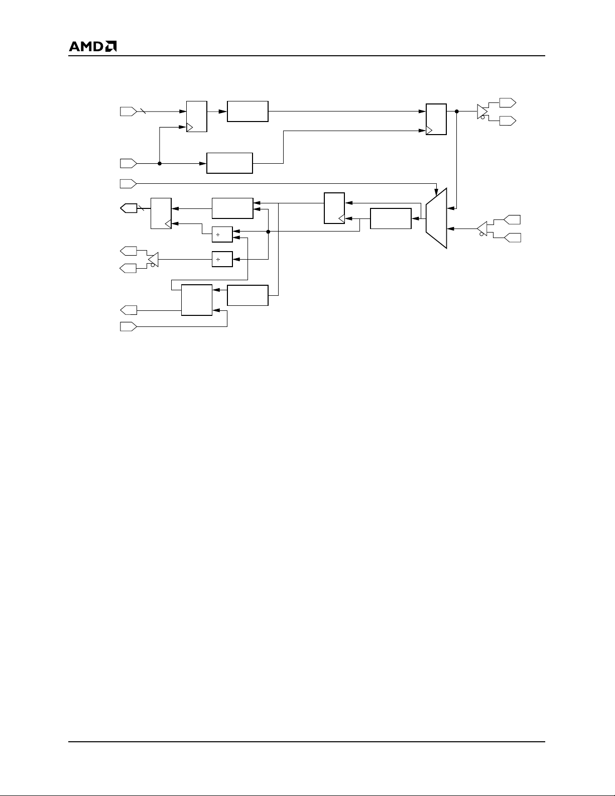
BLOCK DIAGRAM
PRELIMINARY
TXD[0:9]
REFCLK
EWRAP
RXD[0:9]
RCLK
RCLKN
COM_DET
EN_CDET
10
10
Q D
D Q
Frame
Logic
Parallel
to Serial
PLL Clock
Multiply
Serial to
Parallel
10
20
Comma
Detect
Clock
Recovery
TX+
TX-
RX+
RX-
21560A-1
2 Am79761
Page 3
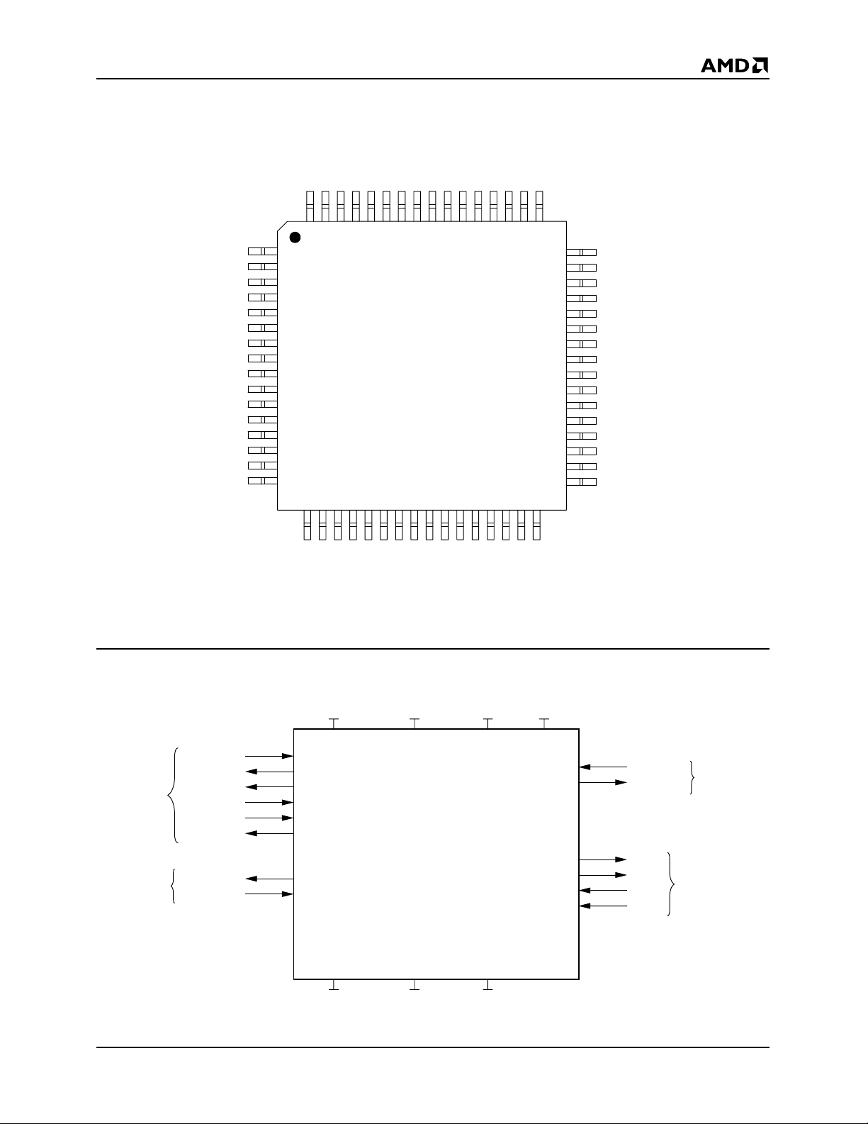
CONNECTION DIAGRAM
PRELIMINARY
N/C
DVDD_P
TX+
TX-
DVDD_P
DVDD
AVSS
AVDD
DVSS
DVDD
RX+
DVDD_P
RX-
DVSS
DVDD
N/C
Note:
N/C = No Connect
DVSS
TXD0
TXD1
TXD2
DVDD
TXD3
TXD4
TXD5
TXD6
DVDD
TXD7
TXD8
TXD9
DVSS
DVSS
N/C
646362616059585756555453525150
1
2
3
4
5
6
7
8
9
10
11
12
13
14
15
16
171819202122232425262728293031
N/C
TEST1
DVSS
TEST2
EWRAP
TEST3
REFCLK
EN_CDET
DVSS
TEST4
N/C
DVDD
DVDD_T
32
RCLK
RCLKN
49
48
47
46
45
44
43
42
41
40
39
38
37
36
35
34
33
DVSS_T
N/C
COM_DET
DVSS_T
RXD0
RXD1
RXD2
DVDD_T
RXD3
RXD4
RXD5
RXD6
DVDD_T
RXD7
RXD8
RXD9
DVSS_T
21560A-2
LOGIC SYMBOL
REFCLK
RCLK
PHY
Control
Test
Port
RCLKN
EN_CDET
EWRAP
COM_DET
TEST4
TDST [3:1]
DVDD DVDD_T DVDD_P AVDD
Am79761
GigaPHY-SD
DVSS DVSS_D DVSS
Am79761 3
TXD [0:9]
RXD [0:9]
TX+
TX–
RX+
RX–
To PCS
Transceiver
21560A-3
Page 4
PRELIMINARY
ORDERING INFORMATION
Standard Products
AMD standard products are available in se veral pac kages and operating ranges . The order number (V alid Combination) is f ormed
by a combination of the elements below.
Am79761
CY
-10
PACKAGE SIZE OPTION
-10 = 10 x 10 mm body size
-14 = 14 x 14 mm body size
TEMPERATURE RANGE
C = Commercial (0˚C to +70˚C)
P ACKA GE TYPE
Y = 64-Pin Plastic Quad Flat Pack (PDH064)
DEVICE NUMBER/DESCRIPTION
Am79761
Physical Layer 10-Bit Transceiver for Gigabit Ethernet
GigaPHY™-SD)
Valid Combinations
Am79761YC
Am79761YC
-10
-14
Valid Combinations
Valid Combinations list configurations planned to be supported in volume for this device. Consult the local AMD sales
office to confirm availability of specific valid combinations and
to check on newly released combinations.
4 Am79761
Page 5

RELATED PRODUCTS
PRELIMINARY
Part No.
Am7990
Am7992B Serial Interface Adapter (SIA)
Am7996 IEEE 802.3/Ethernet/Cheapernet Transceiver
Am79C90 CMOS Local Area Network Controller for Ethernet (C-LANCE)
Am79C98 Twisted Pair Ethernet Transceiver (TPEX)
Am79C100 Twisted Pair Ethernet Transceiver Plus (TPEX+)
Am79C871 Quad Fast Ethernet Transceiver for 100BASE-X Repeaters (QFEXr™)
Am79C981 Integrated Multiport Repeater Plus (IMR+™)
Am79C982 basic Integrated Multiport Repeater (bIMR™)
Am79C983 Integrated Multiport Repeater 2 (IMR2™)
Am79C984A enhanced Integrated Multiport Repeater (eIMR™)
Am79C985 enhanced Integrated Multiport Repeater Plus (eIMR+™)
Am79C987 Hardware Implemented Management Information Base (HIMIB™)
Am79C988A Quad Integrated Ethernet Transceiver (QuIET™)
Am79C900 Integrated Local Area Communications Controller (ILACC™)
Am79C940 Media Access Controller for Ethernet (MACE™)
Am79C960 PCnet™-ISA Single-Chip Ethernet Controller (for ISA bus)
Am79C961 PCnet™-ISA+ Single-Chip Ethernet Controller for ISA (with Microsoft® Plug n’ Play® Support)
Am79C961A PCnet™-ISA II Full Duplex Single-Chip Ethernet Controller for ISA
Am79C965 PCnet™-32 Single-Chip 32-Bit Ethernet Controller
Am79C970 PCnet™-PCI Single-Chip Ethernet Controller (for PCI bus)
Am79C970A PCnet™-PCI II Full Duplex Single-Chip Ethernet Controller (for PCI bus)
Am79C971 PCnet™-
Description
Local Area Network Controller for Ethernet (LANCE)
FAST
Single-Chip Full-Duplex 10/100 Mbps Ethernet Controller for PCI Local Bus
Am79761 5
Page 6
PIN DESIGNATION
Listed by Pin Number
PRELIMINARY
Pin No.
1
2 TXD0 18 TEST1 34 RXD9 50 DVDD
3 TXD1 19 EWRAP 35 RXD8 51 DVSS
4 TXD2 20 TEST2 36 RXD7 52 RX5 DVDD 21 DVSS 37 DVDD_T 53 DVDD_P
6 TXD3 22 REFCLK 38 RXD6 54 RX+
7 TXD4 23 TEST3 39 RXD5 55 DVDD
8 TXD5 24 EN_CDET 40 RXD4 56 DVSS
9 TXD6 25 DVSS 41 RXD3 57 AVDD
10 DVDD 26 TEST4 42 DVDD_T 58 AVSS
11 TXD7 27 N/C 43 RXD2 59 DVDD
12 TXD8 28 DVDD 44 RXD1 60 DVDD_P
13 TXD9 29 DVDD_T 45 RXD0 61 TX14 DVSS 30 RCLKN 46 DVSS_T 62 TX+
15 DVSS 31 RCLK 47 COM_DET 63 DVDD_P
16 N/C 32 DVSS_T 48 N/C 64 N/C
Pin Name Pin No. Pin Name Pin No. Pin Name Pin No. Pin Name
DVSS 17 N/C 33 DVSS_T 49 N/C
6 Am79761
Page 7

PRELIMINARY
PIN DESCRIPTION
TX+, TXSerial T ransmit Data
PECL Output
These pins are the 1000BASE-X port differential drivers which transmit the serial stream to the network.
These pins are connected to the copper or fiber optic
connectors.
When EWRAP is LOW, the pins assume normal operation. When HIGH, TX+ is logic HIGH and TX- is logic
LOW.
RX+, RXSerial Receive Data
PECL Input
These pins are the 1000BASE-X port differential receiver pair, receiving a serial stream of data from the
network. These pins are connected to the copper or
fiber optic connectors.
When EWRAP is LOW, the pins assume normal operation. The pins are internally biased.
TXD[0:9]
Transmit Data
TTL Input
The TXD[0:9] pin is a set of 10 data signals which are
driven from the Physical Coding Subla yer (PCS) abov e.
The 10 bits of data are clocked in parallel on the rising
edge of REFCLK. TXD0 is transmitted first on TX ± .
RXD[0:9]
Receive Data
TTL Output
The RXD[0:9] pin is a set of 10 data signals which are
sent to the Physical Coding Subla yer (PCS) abov e. The
10 bits of data are clocked out in parallel on the rising
edges of RCLK and RCLKN. RXD0 is received first on
RX ± .
REFCLK
Reference Clock
TTL Input
This input is used for the 125-Mhz clock. The rising
edge of this clock latches TXD[0:9] into an input register. This clock serves as the reference clock at 1/10th
the baud rate for the PLL.
RCLK, RCLKN
Receive Clock
TTL Output
These pins provide the differential receive clock signals, derived from the RX ± data stream, and are at
1/20th the baud rate of the receive stream. P arallel data
on RXD[0:9] is provided at each rising transition of
RCLK and RCLKN.
EN_CDET
Enable Comma Detect
TTL Input
This pin is used to enable the word synchronization
mode. When logic HIGH, the COM_DET output is enabled and word synchronization is active.
COM_DET
Comma Detect Indicator
TTL Output
Comma Detect is asserted to indicate that the incoming
word on RXD[0:9] contains a Comma character
(0011111xxx). COM_DET goes HIGH f or half of a RCLK
period, and can be captured when RCKLN is rising.
In order for COM_DET to provide indication, EN_CDET
must be enabled (logic HIGH).
EWRAP
Loopback Enable
TTL Input
When EWRAP is asserted, the transmitted data stream
is sent back to the receiver through an internal loopback path. TX+ is logic HIGH, and TX- is logic LOW in
this mode.
This pin is logic LOW for normal operation.
TEST[1:3]
Factory Test Pins
Input
These pins should be tied to DVDD f or normal operation.
TEST[4]
Factory Test Pin
Output
This pin should be left unconnected for normal operation.
DVDD
Power
These pins supply power to the digital blocks of the
device. They m ust be connected to a 3.3 V ± 5% source.
DVDD_T
TTL Power
These pins supply power to the TTL blocks of the device. They must be connected to a 3.3 V ± 5% source.
DVDD_P
PECL Power
These pins supply power to the PECL blocks of the device. They must be connected to a 3.3 V ± 5% source. It
is critical that the signal supplied to these pins are
clean to ensure good performance of the device.
Am79761 7
Page 8

PRELIMINARY
AVDD
Analog Power
These pins supply power to the analog blocks of the
device. They must be connected to a 3m.3 V ± 5%
source and require careful decoupling to ensure
proper device performance.
DVSS
Ground
These pins are the ground connections for the digital
blocks. They must be connected to the common
external ground plane.
DVSS_T
Ground
These pins are the ground connections for the TTL
blocks. They must be connected to the common external ground plane.
AVSS
Ground
These pins are the ground connections for the
analog blocks. They must be connected to an analog
ground plane.
8 Am79761
Page 9

PRELIMINARY
FUNCTIONAL DESCRIPTION
Overview
The GigaPHY-SD device provides the PMA functionality
for 1000BASE-X systems. The GigiaPHY-SD communicates with the PCS through the 10-bit code groups and
communicates with the Physical Medium Dependent
(PMD) layer to transmit and receive data from the network, through either fiber optic or copper coax media.
The GigaPHY-SD device consists of the following
functional blocks:
n
1000BASE-X Transmit block including:
— Clock Synthesizer
— Serializer and Transmission interface
n
1000BASE-X Receive block including:
— Clock Recovery
— Deserializer
— Word Alignment and synchronization
Table 20. Transmission Order and Mapping of an 8B/10B Character
Clock Synthesizer
The Am79761 clock synthesizer multiplies the reference frequency provided on the REFCLK pin by 10 to
achieve a baud rate clock at nominally 1.25 GHz. The
clock synthesizer contains a fully monolithic PLL which
does not require any external components.
Serializer
The Am79761 device accepts TTL input data as a parallel 10-bit character on the TXD[0:9] bus which is
latched into the input latch on the rising edge of
REFCLK. This data will be serialized and transmitted
on the TX PECL differential outputs at a baud rate of
ten times the frequency of the REFCLK input, with bit
TXD0 transmitted first. User data should be encoded
for transmission using the 8B/10B block code described in the IEEE 802.3 specification.
Transmission Character Interface
An encoded byte is 10 bits and is referred to as a transmission character. The 10-bit interface on the
Am79761 device corresponds to a transmission character. This mapping is shown in Table 20.
Parallel Data Bits T9 T8 T7 T6 T5 T4 T3 T2 T1 T0
8B/10B Bit Position j h g f i e d c b a
Comma Character X X X 1111100
Last Data Bit
Transmitted
Clock Recovery
The Am79761 device accepts differential high speed
serial inputs on the RX ± pins, extracts the clock and
retimes the data. The Am79761 cloc k recov ery circuitry
is completely monolithic and requires no external components. For proper operation, the baud rate of the
data stream to be recovered should be within 0.01% of
ten times the REFCLK frequency. For example, if the
REFCLK used is 125 MHz, then the incoming serial
baud rate must be 1.25 gigabaud ± 0.01 percent.
Deserializer
The re-timed serial bit stream is converted into a 10-bit
parallel output character. The Am79761 device provides
complementary TTL recovered clocks, RCLK and
RCLKN, which are at 1/20th of the serial baud rate. This
architecture is designed to simplify demultiplexing of the
10-bit data characters into a 20-bit half-word in the
downstream controller chip. The clocks are generated b y
dividing down the high-speed clock which is phase
locked to the serial data. The serial data is re-timed by
the internal high-speed clock and deserialized.
The resulting parallel data will be captured by the
adjoining protocol logic on the rising edges of RCLK and
RCLKN. In order to maximize the setup and hold times
available at this interf ace , the parallel data is loaded into
the output register at a point nominally midway between
the transition edges of RCLK and RCLKN.
If serial input data is not present or does not meet the
required baud rate, the Am79761 will continue to produce a recovered clock so that do wnstream logic may
continue to function. The RCLK and RCLKN output
frequency under these circumstances may differ from
their expected frequency by no more than ± 1 percent.
First Data Bit
Transmitted
Am79761 9
Page 10

PRELIMINARY
Word Alignment
The Am79761 device provides 7-bit comma character
recognition and data word alignment. Word synchronization is enabled by asserting EN_CDET HIGH. When
synchronization is enabled, the Am79761 device constantly examines the serial data for the presence of the
Comma character. This pattern is 0011111XXX, where
the leading zero corresponds to the first bit received.
The comma sequence is not contained in any normal
8B/10B coded data character or pair of adjacent characters. It occurs only within special characters, known
as K28.1, K28.5, and K28.7, which are defined specifically for synchronization purposes. Improper alignment
of the comma character is defined as any of the following conditions:
1. The comma is not aligned within the 10-bit transmission character such that TXD0...TXD6 =
“0011111.”
2. The comma straddles the boundary between two
10-bit transmission characters.
3. The comma is properly aligned but occurs in the received character presented during the rising edge
of RCLK rather than RCLKN.
When EN_CDET is HIGH and an improperly aligned
comma is encountered, the internal data is shifted in
such a manner that the comma character is aligned
properly in RXD[0:9]. This results in proper character
and half-word alignment. When the parallel data
alignment changes in response to an improperly
aligned comma pattern, some data which would have
been presented on the parallel output port may be
lost. However, the synchronization character and
subsequent data will be output correctly and properly
aligned. When EN_CDET is LOW, the current alignment of the serial data is maintained indefinitely,
regardless of data pattern.
When encountering a comma character, COM_DET is
driven HIGH to inform the user that realignment of the
parallel data field may have occurred. The COM_DET
pulse is presented simultaneously with the comma character and has a duration equal to the data, or half of an
RCLK period. The COM_DET signal is timed such that it
can be captured by the adjoining protocol logic on the
rising edge of RCLKN. Functional waveforms for
synchronization are given in Figure 18 and Figure 19.
Figure 18 shows the case when a comma character is
detected and no phase adjustment is necessary. It illustrates the position of the COM_DET pulse in relation to
the comma character on RXD[0:9]. Figure 19 sho ws the
case where K28.5 is detected, but it is out of phase and
a change in the output data alignment is required. Note
that up to three characters prior to the comma character
may be corrupted by the realignment process.
RCLK
RCLKN
COM_DET
RXD[0:9]
Note : TChar = 10-bit Transmission Character
Figure 18. Detection of a Properly Aligned Comma Character
K28.5 TChar TChar TChar
21560A-4
10 Am79761
Page 11

RCLK
RCLKN
COM_DET
PRELIMINARY
RXD[0:9]
K28.5 K28.5TChar TChar TChar TChar
Potentially Corrupted
21560A-5
Figure 19. Receiving Two Consecutive K28.5 + TCharacter Transmission Words
Am79761 11
Page 12

µ
µ
∆
∆
∆
PRELIMINARY
ABSOLUTE MAXIMUM RATINGS
Storage Temperature . . . . . . . . . . . .-65 ° C to +150 ° C
Ambient Temperature Under Bias . .-55 ° C to +125 ° C
Power Supply Voltage (V
DC Voltage (PECL Inputs) . . . . . .-0.5 V to V
DC Voltage (TTL Inputs). . . . . . . . . . . -0.5 V to +5.5 V
) . . . . . . . -0.5 V to +4.0 V
DD
DD
+0.5 V
OPERATING RANGES
Temperature (T
. . . . . . . . . . . . .0 ° C to +50 ° C for 10 x 10 mm PQFP
Power Supply Voltage (D
Operating ranges define those limits between which
functionality of the device is guaranteed.
) 0 ° C to +70 ° C for 14 x 14 mm PQFP
A
) . . . . . . . . . +3.3 V ± 5%
VDD
Output Current (TTL Outputs) . . . . . . . . . . . .- ± 50 mA
Output Current (PECL Outputs). . . . . . . . . . .- ± 50 mA
Maximum Input ESD (Human Body Model). . . 1500 V
Stresses above those listed under Absolute Maximum
Ratings may cause permanent device failure.
Functionality at or above these limits is not implied.
Exposure to absolute maximum ratings for extended
periods may affect device reliability.
DC CHARACTERISTICS (over recommended operating conditions)
Symbol Parameter Description Test Conditions Min Typ Max Unit
V
V
I
IH
I
IL
V
V
I
DD
P
IH
IL
OH
OL
V
OUT75
V
OUT50
V
IN
D
Input HIGH voltage (TTL) 2.0 — 5.5 V
Input LOW voltage (TTL) 0 — 0.8 V
Input HIGH current (TTL) V
Input LOW current (TTL) V
Output HIGH voltage (TTL) I
Output LOW voltage (TTL) I
TX Output differential peak-to-
peak voltage swing
TX Output differential peak-to-
peak voltage swing
Receiver differential peak-to-
peak Input Sensitivity RX
Supply Current
Power dissipation
=2.4 V — 50 500
IN
=0.5 V — — -500
IN
= -1.0 mA 2.4 — — V
OH
= +1.0 mA — — 0.5 V
OL
75 Ω to V
50 Ω to V
Internally biased to V
Outputs open,
V
= V
DD
Outputs open,
V
= V
DD
– 2.0 V 1200 — 2200 mVp-p
DD
– 2.0 V 1200 — 2200 mVp-p
DD
/2 400 — 3200 mVp-p
DD
DD
DD
max
max
— 210 290 mA
— 700 1000 mW
A
A
12 Am79761
Page 13

PRELIMINARY
INPUT
REFCLK and TTL Inputs
D
D
VDD
VSS
A
INPUT
Current
Limit
R
INPUT
R
Figure 20. Input Structures
D
VDD
D
VSS
High Speed Differential Input
(RX±)
B
All Resistors
3.3K
21560A-6
Am79761 13
Page 14

PRELIMINARY
KEY TO SWITCHING WAVEFORMS
WAVEFORM INPUTS OUTPUTS
AC CHARACTERISTICS
REFCLK
Must be
Steady
May
Change
from H to L
May
Change
from L to H
Don’t Care,
Any Change
Permitted
Does Not
Apply
Will be
Steady
Will be
Changing
from H to L
Will be
Changing
from L to H
Changing,
State
Unknown
Center
Line is HighImpedance
“Off” State
KS000010-PAL
T
T
1
2
TXD[0:9]
10 Bit Data
Data Valid Data Valid Data Valid
Figure 21. Transmit Timing Waveforms
Table 21. Transmit AC Characteristics
Symbol Parameter Description Test Conditions Min Max Unit
Measured between the valid data
level of TXD[0:9] to the 1.4 V point of
REFCLK
20% to 80%, 75 Ω load to V
, T ested
SS
on a sample basis
bc = Bit clocks
ns = Nano second
1.5 — ns
1.0 — ns
— 300 ps
11bc - 1ns — —
T
1
T
2
T
SDR,TSDF
T
LAT
TXD[0:9] Setup time to the rising
edge of REFCLK
TXD[0:9] hold time after the rising
edge of REFCLK
TX± rise and fall time
Latency from rising edge of
REFCLK to TXD0 appearing on
TX±-
21560A-7
14 Am79761
Page 15

PRELIMINARY
AC CHARACTERISTICS (Continued)
RCLK
RCLKN
T
4
T
3
RXD[0:9]
T
1
Data Valid Data Valid Data Valid
T
2
Figure 22. Receive Timing Waveform
Table 22. Receive AC Characteristics
Symbol Parameter Description Test Conditions Min Max Unit
T
1
T
2
Data or COM_DET Valid prior
to RCLK/RCLKN rise
Data or COM_DET Valid after
RCLK or RCLKN rise
Deviation of RCLK rising edge
to RCLKN rising edge delay
T
3
from nominal.
delay
f
baud
----------- T
±=
10
3
Deviation of RCLK, RCLKN
frequency from nominal.
T
4
f
RCLK
f
REFCLK
------------------- -T
±=
2
Measured between the 1.4 V
point of RCLK or RCLKN and a
valid level of RXD[0:9]. All
outputs driving 10 pF load.
Nominal delay is 10 bit times.
Tested on sample basis
Whether or not locked to serial
data
4
3.0 — ns
2.0 — ns
-500 500 ps
-1.0 1.0 %
21560A-8
T
, T
R
F
R
lat
T
LOCK
Receive Data
Jitter
RXD[0:9], COM_DET, RCLK,
RCLKN rise and fall time
Latency from RX± to RXD[0:9]
Data acquisition lock time @
1.25 Gbps
Between V
IL(MAX)
into 10 pf load.
bc = Bit clock
ns = Nano second
8B/10B IDLE pattern.
Tested on a sample basis
Receive Data Jitter Power dBc, RMS for 10
1
------------------------------- 2 BitTime×
∫
100KHz
PhaseNoise
Ratio Tested on a sample basis
Am79761 15
and V
-12
Bit Error
IH(MIN)
,
— 2.4 ns
15 bc + 2 ns 34 bc + 2 ns —
— 2.0
—40ps
µs
Page 16

PRELIMINARY
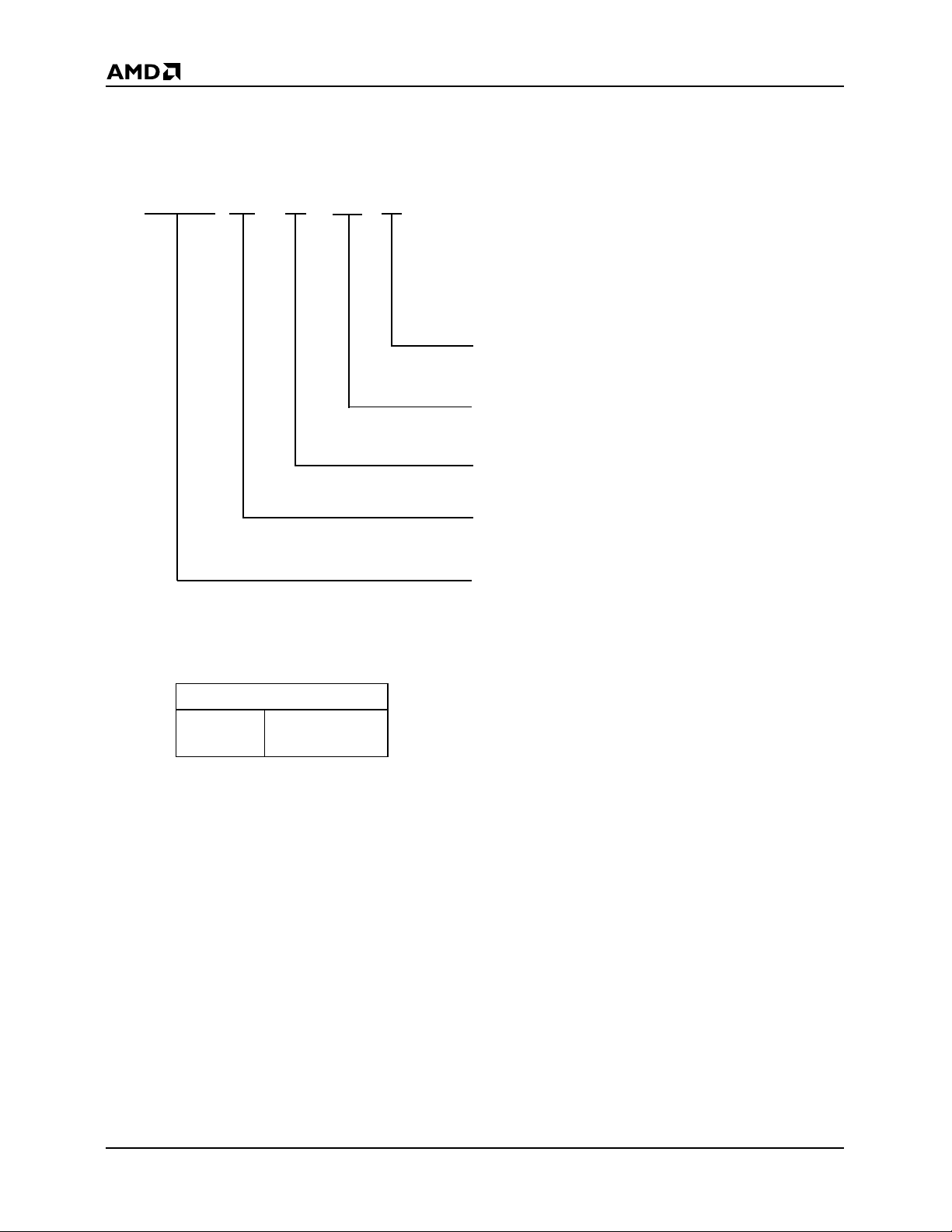
REFERENCE CLOCK REQUIREMENTS
REFCLK
T
L
T
H
V
(min)
V
ih
(max)
il
21560A-9
Figure 23. REFCLK Timing Waveform
Table 23. Reference Clock Requirements
Symbol Parameter Description Test Conditions Min Max Units
Range over which both transmit and
FR Frequency Range
FO Frequency Offset
DC REFCLK duty cycle Measured at 1.5 V 30 70 %
T
RCR,TRCF
REFCLK rise and fall time Between V
receive reference clocks on an y link may be
centered
Maximum frequency offset between
transmit and receive reference clocks on
one link
and V
IL(MAX)
IH(MIN)
123 127 MHz
-200 200 ppm
— 1.0 ns
16 Am79761
Page 17

MEASUREMENTS
PRELIMINARY
Serial Input Rise and Fall Time
T
r
T
f
Receiver Input Eye Diagram Jitter Tolerance Task Mask
Amplitude
Parametric Test Load Circuit
80%
20%
Eye Width%
TTL Input and Output Rise and Fall Time
T
r
T
f
Bit Time
TTL AC Output LoadSerial Output Load
V
ih(min)
V
il(max)
Z
= 75W
0
V
DD
75Ω
– 2.0 V
10 pF
Figure 24. Parametric Measurement Information
21560A-10
Am79761 17
Page 18

MEASUREMENTS (Continued)
PRELIMINARY
Random Jitter Measurement
BERT
Pattern
Generator
CLK = 1.25 GHz
DATA = 00000 0000011111 11111
-K28.7
0011111000
Random jitter (RJ) measurements performed according to Fibre Channel 4.3 Annex A, Test Methods, Section
A.4.4. Measure standard deviation of all 50% crossing points. Peak to peak RJ is
BERT
Pattern
Generator
CLK = 1.25 GHz
DATA = 00000 0000011111 11111
RJ
-K28.7
0011111000
DATA
PAT SYNC
DATA
DATA
125 MHz
125 MHz
Am79761
REFCLK TX+
TXD[0:9]
Deterministic Jitter Measurement
125 MHz
125 MHz
TX-
Trigger
Digitizing
Scope
1.25 Gbps
Single-Ended Measurement
±
7 sigma of distribution.
Trigger
Digitizing
Scope
-K28.5
0011111010
TRIGGER
DATA
2 bit time
Figure 25. Transmitter Jitter Measurement Method
Transmitter Output Jitter Allocation
T
rj
T
DJ
Serial data output random jitter
(RMS)
Serial data output deterministic
jitter (p-p)
DJ
K28.5
1100000101
8 bit time
7 bit time
Am79761
REFCLK TX+
TXD[0:9]
20 bit time
19 bit time
18 bit time
17 bit time
12 bit time
10 bit time
9 bit time
TX-
Deterministic jitter (DJ) measurements
performed according to Fibre Channel
4.3 Annex A, Test Methods, Section A.4.3.
Measure time of all the 50% points of
all ten transitions. DJ is the range of
the timing variation from expected.
RMS, tested on a sample basis
(refer to Figure 8)
Peak to peak, tested on a sample
basis (refer to Figure 8)
1.25 Gbps
Single-Ended Measurement
21560A-11
—20ps
— 100 ps
18 Am79761
Page 19

PRELIMINARY
THERMAL CONSIDERATIONS
The Am79761 is packaged in a 14-mm or a 10-mm
conventional PQFP with an internal heat spreader. These
packages use an industry-standard EIAJ footprint, but
have been enhanced to improve thermal dissipation. The
construction of the packages are as shown in Figure 26.
Copper Heat SpreaderPlastic Molding Compound
Lead
Bond Wire
Die
Figure 26. Package Cross Section
Table 24. Thermal Resistance
Symbol Description 10 mm Value 14 mm Value Units
θ
jc
θ
ca
θ
ca-100
θ
ca-200
θ
ca-400
θ
ca-600
The Am79761 is designed to operate with a junction
temperature up to 105oC. The user must guarantee
that the temperature specification is not violated. With
the Thermal Resistances shown above, the 10x10
PQFP can operate in still air ambient temperatures of
Notes:
o
1. 50
C=110oC-1W*(10oC/W+50.8oC/W)
o
2. 72
C=110oC-1W*(95oC/W+29oC/W)
Thermal resistance from junction to case 10.0 9.5
Thermal resistance from case to ambient in still air including
conduction through the leads.
50.8 29
Thermal resistance from case to ambient with 100 LFM airflow 41.2 26.1
Thermal resistance from case to ambient with 200 LFM airflow 36.9 23.8
Thermal resistance from case to ambient with 400 LFM airflow 31.8 20.5
Thermal resistance from case to ambient with 600 LFM airflow 27.8 17.9
50oC, while the 14x14 PQFP can operate in still air ambient temperatures of 72oC. If the ambient air temper ature exceeds these limits then some form of cooling
through a heatsink or an increase in airflow must be
provided.
21560A-12
o
C/W
o
C/W
o
C/W
o
C/W
o
C/W
o
C/W
Am79761 19
Page 20

PRELIMINARY
PHYSICAL DIMENSIONS
PDH064
64-Pin (measured in millimeters)
Trademarks
Copyright © 1998 Advanced Micro Devices, Inc. All rights reserved.
AMD, the AMD logo, and combinations thereof are trademarks of Advanced Micro Devices, Inc.
GigaPHY is a trademark of Advanced Micro Devices, Inc.
Product names used in this publication are for identification purposes only and may be trademarks of their respective companies.
20 Am79761
 Loading...