

Page 1
Philips Semiconductors Linear Products Product specification
AM601212-Bit multiplying D/A converter
776
August 31, 1994 853-0904 13721
DESCRIPTION
The AM6012 12-bit multiplying Digital-to-Analog converter provides
high-speed and 0.025% differential nonlinearity over its full
commercial temperature range.
The D/A converter uses a 3-bit segment generator for the MSBs in
conjunction with a 9-bit R-2R diffused resistor ladder to provide
12-bit resolution without costly trimming processes. This technique
guarantees a very uniform step size (up to ± LSB from the ideal),
monotonicity to 12 bits and integral nonlinearity to 0.05% at its
differential current outputs.
The dual complementary outputs of the AM6012 increase its
versatility, and effectively double the peak-to-peak output swing.
Digital inputs, in addition, can be configured to accept all popular
logic families.
While the device requires a reference input of 1mA for a 4mA
full-scale current, operation is nearly independent of power supply
voltage shifts. The power supply rejection ratio is ±0.001% FS/% ∆V.
The devices will work from +5, -12V to ±18V rails, with as low as
230mW power consumption typical.
FEATURES
•12-bit resolution
•Accurate to within ±0.05%
•Monotonic over temperature
•Fast settling time, 250ns typical
•Trimless design for low cost
•Differential current outputs
•High-speed multiplying capability
•Full-scale current, 4mA (with 1mA reference)
•High output compliance voltage, -5 to +10V
•Low power consumption, 230mW
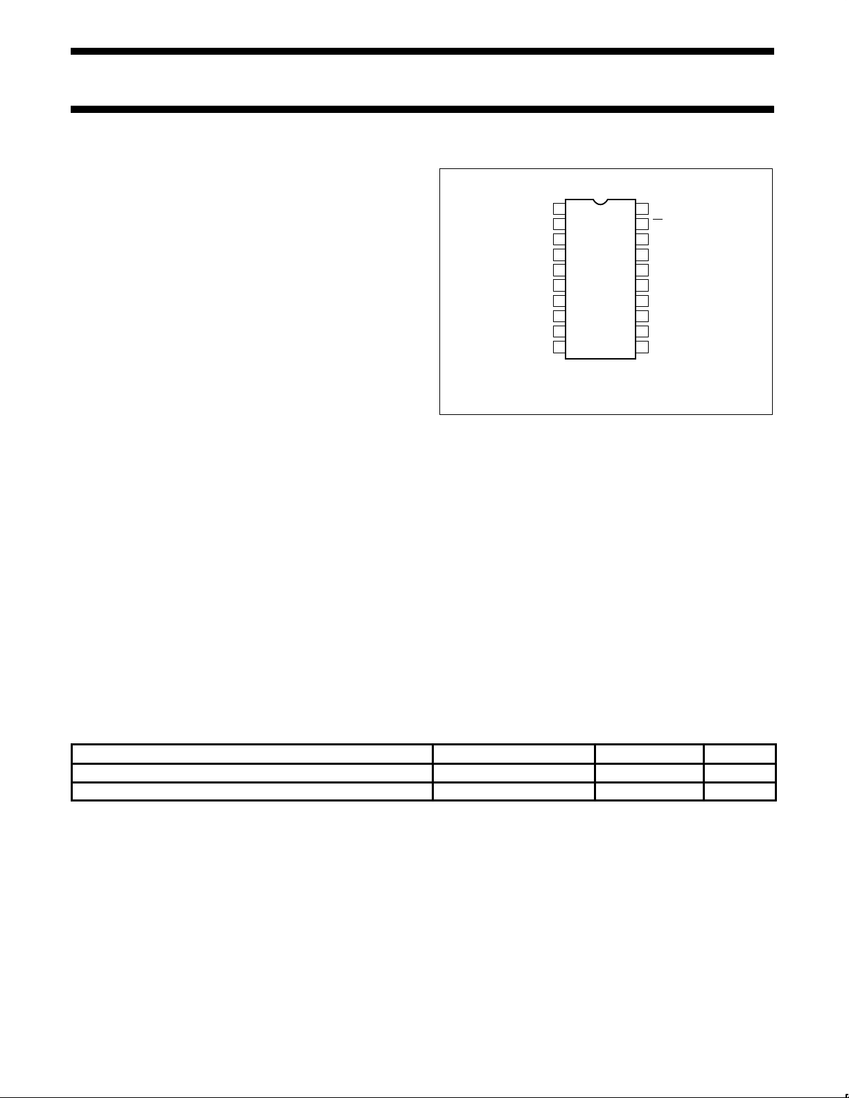
PIN CONFIGURATION
1
2
3
4
5
6
7
8
9
10
11
12
13
14
20
19
18
17
16
15
D1 and F Packages
NOTE:
1. Available in large SO (SOL) package only.
TOP VIEW
D
1
D
2
D
3
D
4
D
5
D
6
D
7
D
8
D
9
D
10
V+
I
O
I
O
V–
COMP
V
REF(–)
V
REF(+)
GND/V
LC
D12 LSB
D
11
APPLICATIONS
•CRT displays, computer graphics
•Robotics and machine tools
•Automatic test equipment
•Programmable power supplies
•CAD/CAM systems
•Data acquisition and control systems
•Analog-to-digital converter systems
ORDERING INFORMATION
DESCRIPTION TEMPERATURE RANGE ORDER CODE DWG #
20-Pin Ceramic Dual In-Line Package (CERDIP) 0 to +70°C AM6012F 0584B
20-Pin Plastic Small Outline Large (SOL) Package 0 to +70°C AM6012D 0172D
Page 2
Philips Semiconductors Linear Products Product specification
AM601212-Bit multiplying D/A converter
August 31, 1994
777
BLOCK DIAGRAM
COMP V(–)
16 17
V
REF
(+)
V
REF
(–)
14
15
BIAS
NETWORK
REFERENCE
AMPLIFIER
9-SEGMENT
GENERATOR
DECODER
CURRENT
SWITCHES
I
SEG
9-BIT R-2R
D/A CONVERTER
LOGIC SWITCHES
18
19
I
O
I
O
12111098765432113
LSBGND/MSB
20
V(+)
V
LC
B12B11B10B9b8B7B6B5B4B3B2B1
ABSOLUTE MAXIMUM RATINGS
SYMBOL PARAMETER RATING UNIT
T
A
Operating temperature
AM6012F 0 to +70 °C
T
STG
Storage temperature range -65 to +150 °C
T
SOLD
Lead soldering temperature 10sec max 300 °C
V
S
Power supply voltage ±18 V
Logic inputs -5V to +18 V
Voltage across current outputs -8V to +12 V
V
REF
Reference inputs V14, V
15
V- to V+
V
REF
Reference input differential voltage (V14 to V15) ±18 V
I
REF
Reference input current (I14) 1.25 mA
P
D
Maximum power dissipation, TA=25°C, (still-air)
1
F package 1560 mW
D package 1390 mW
NOTES:
1. Derate above 25°C, at the following rate:
F package at 12.5mW/°C
D package at 11.1mW/°C
Page 3
Philips Semiconductors Linear Products Product specification
AM601212-Bit multiplying D/A converter
August 31, 1994
778
DC ELECTRICAL CHARACTERISTICS
V+=+15V, V-=-15V, I
REF
=1.0mA, 0°C ≤ T
A
≤ 70°C
LIMITS
SYMBOL
PARAMETER
TEST CONDITIONS
Min Typ Max
UNIT
Resolution 12 Bits
Monotonicity 12 Bits
DNL Differential nonlinearity Deviation from ideal step size ±0.025 %FS
12 Bits
NL Nonlinearity Deviation from ideal straight line ±.05 %FS
I
FS
Full-scale current
V
REF
=10.000V
R
14-R15
=10.000kΩ
T
A
=25°C
3.935 3.999 4.063 mA
TCI
FS
Full-scale tempco ±10 ±40 ppm/°C
±0.001 ±0.004 %FS/°C
V
OC
Output voltage compliance
DNL Specification guaranteed over
compliance range
R
OUT
>10MΩ typ.
-5 +10 V
I
FSS
Symmetry IFS-I
FS
±0.4 ±2.0 µA
I
ZS
Zero-scale current 0.10 µA
V
IL
V
IH
Logic
input
levels
Logic “0” 0.8 V
Logic “1” 2.0
I
IN
Logic input current VIN=-5 to +18V 40 µA
V
IS
Logic input swing V-=-15V -5 +18 V
I
REF
Reference current range 0.2 1.0 1.1 mA
I
15
Reference bias current 0 -0.5 -2.0 µA
dl/dt Reference input slew rate
R
14(eq)
=800Ω
C
C
=0pF
4.0 8.0 mA/µs
PSSI
FS+
Power supply sensitivity V+=+13.5V to +16.5V, V-=-15V ±0.0005 ±0.001 %FS/%
PSSI
FS-
V-=-13.5V to -16.5V, V+=+15V ±0.00025 ±0.001
V+ Power supply range V
OUT
=0V 4.5 18 V
V- -18 -10.8
I+ V+=+5V, V-=-15V 5.7 8.5
I- Power supply current -13.7 -18.0 mA
I+ V+=+15V, V-=-15V 5.7 8.5
I- -13.7 -18.0
P
D
Power dissipation V+=+5V, V-=-15V 234 312 mW
V+=+15V, V-=-15V 291 397
AC ELECTRICAL CHARACTERISTICS
V+=+15V, V-=-15V, I
REF
=1.0mA, 0°C ≤ T
A
≤ 70°C
LIMITS
SYMBOL
PARAMETER
TEST CONDITIONS
Min Typ Max
UNIT
t
S
Settling time To ± 1/2LSB, all bits ON or OFF, TA=25°C 250 500 ns
t
PLH
t
PHL
Propagation
delay—all bits
50% to 50% 25 50 ns
C
OUT
Output capacitance 20 pF
Page 4

Philips Semiconductors Linear Products Product specification
AM601212-Bit multiplying D/A converter
August 31, 1994
779
CIRCUIT DESCRIPTION
The AM6012 is a 12-bit DAC which uses diffused resistors and
requires no trimming to guarantee monotonicity over the
temperature range. A segmented DAC design guarantees a more
uniform step size over the temperature range than is normally
available with trimmed 12-bit converters. The converter features
differential high compliance current outputs, wide supply range, and
a multiplying reference input.
In many converter applications, uniform step size is more important
than conformance to an ideal straight line. Many 12-bit converters
are used for high resolution rather than high linearity, since few
transducers are more linear than ±0.1%. All classic binarily weighted
converters require ±1/2LSB (±0.012%) linearity in order to guarantee
monotonicity, which requires very tight resistor matching and
tracking. The AM6012 uses conventional bipolar processing to
achieve high differential linearity and monotonicity without requiring
correspondingly high linearity, or conformance to an ideal straight
line.
One design approach which provides monotonicity without requiring
high linearity is the MOS switch-resistor string. This circuit is actually
a full complement to a current-switched R-2R DAC since it is slower,
has a voltage output, and, if implemented at the 12-bit level, would
use 4096 low tolerance resistors rather than a minimum number of
high tolerance resistors as in the R-2R network. Its lack of speed
and density for 12 bits are its drawbacks.
With the segmented DAC approach, the 4096 required output levels
are composed of 8 groups of 512 steps each. Each step group is
generated by a 9-bit DAC, and each of the segment slopes is
determined by one of 8 equal current sources. The resistors which
determine monotonicity are in the 9-bit DAC. The major carry of the
9-bit DAC is repeated in each of the 8 segments, and requires eight
times lower initial resistor accuracy and tracking to maintain a given
differential nonlinearity over temperature.
The operation of the segmented DAC may be visualized by
assuming an input code of all zeroes. The first segment current I
O
is
divided into 512 levels by the 9-bit multiplying DAC and fed to the
output, I
OUT
. As the input code increases, a new segment current is
selected for each 512 counts. The previous segment is fed to output
I
OUT
where the new step group is added to it, thus ensuring
monotonicity independent of segment resistor values. All higher
order segments feed I
OUT
.
With the segmented DAC approach, the precision of the 8 main
resistors determines linearity only. The influence of each of these
resistors on linearity is four times lower than that of the MSB resistor
in an R-2R DAC. Hence, assuming the same resistor tolerances for
both, the linearity of the segmented approach would actually be
higher than that of an R-2R design.
The step generator or 9-bit DAC is composed of a master and a
slave ladder. The slave ladder generates the four least significant
bits from the remainder of the master ladder by active current
splitting utilizing scaled emitters. This saves ladder resistors and
greatly reduces the range of emitter scaling required in the 9-bit
DAC. All current switches in the step generator are high-speed
fully-differential switches which are capable of switching low currents
at high speed. This allows the use of a binary scaled network all the
way to the least significant bit which saves power and simplifies the
circuitry.
Diffused resistors have advantages over thin film resistors beyond
simple economy and bipolar process compatibility. The resistors are
fabricated in single crystal rather than amorphous material which
gives them better long term stability and tracking and much higher
moisture resistance. They are diffused at 1000°C and so are
resistant to changes in value due to thermal and chemical causes.
Also, no burn-in is required for stability. The contact resistance
between aluminum and silicon is more predictable than between
aluminum and an amorphous thin film, and no sandwich metals are
required to enhance or protect the contact or limit alloying. The initial
match between two diffused resistors is similar to that of thin film
since both are defined by photomasks and chemical etching. Since
the resistors are not trimmed or altered after fabrication, their
tracking and long-term characteristics are not degraded.
DIFFERENTIAL VS INTEGRAL NONLINEARITY
Integral nonlinearity, for the purposes of the discussion, refers to the
“straightness” of the line drawn through the individual response
points of a data converter. Differential nonlinearity, on the other
hand, refers to the deviation of the spacing of the adjacent points
from a 1 LSB ideal spacing. Both may be expressed as either a
percentage of full-scale output or as fractional LSBs or both. The
graphs in Figure 1 define the manner in which these parameters are
specified. The left graph shows a portion of the transfer curve of a
DAC with 1/2LSB INL and the (implied) DNL spec of 1 LSB. Below
this is a graphic representation of the way this would appear on a
CRT screen where the AM6012 is used as a display driver. On the
right is a portion of the transfer curve of a DAC specified for 1/2LSB
INL with LSB DNL specified and the graphic display below it.
One of the characteristics of an R-2R DAC in standard form is that
any transition which causes a zero LSB change (i.e., the same
output for two different codes) will exhibit the same output each time
that transition occurs. The same holds true for transitions causing a
2 LSB change. These two problem transitions are allowable for the
standard definition of monotonicity and also allow the device to be
specified very tightly for INL. The major problem arising from this
error type is in A/D converter implementations. Inputs producing the
same output are now represented by ambiguous output codes for an
identical input. Also, two LSB gaps can cause large errors at those
input levels (assuming 1/2LSB quantizing levels). It can be seen
from the two figures that the DNL-specified D/A converter will yield
much finer grained data than the INL-specified part, thus improving
the ability of the A/D to resolve changes in the analog input.
Page 5

Philips Semiconductors Linear Products Product specification
AM601212-Bit multiplying D/A converter
August 31, 1994
780
DIFFERENTIAL LINEARITY COMPARISON
ANALOG OUT
Figure 1. Differential Linearity Comparison
±1/2LSB INL, ±1LSB DNL ±2LSB INL, ±1LSB DNL
0000 0010 0100 0110 1000 1010 1100 1110
0001 0011 0101 0111 1001 1011 1101 1111
IDEAL OUTPUTS
ACUTAL OUTPUTS
+1/2LSB
LIMIT
2LSB CHANGE ON
X011–X100
TRANSITION
SEGMENT
OF 12-BIT
DAC TRANSFER
CURVE FOR:
NO CHANGE ON
XX01–XX10 TRANSITION
–1/2LSB LIMIT
DIGITAL INPUT
ANALOG OUT
INL = ±1/2LSB
DNL = ±1LSB
0010 0010 0100 0110 1000 1010 1100 1110
0001 0011 0101 0111 1001 1011 1101 1111
DNL = ±ℑ√2LSB
INL = ±2LSB
SEGMENT OF 12-BIT DAC
TRANSFER CURVE FOR:
–2 LSB
LIMIT
SEGMENT
CHANGE
IDEAL OUTPUTS
ACUTAL OUTPUTS
SEGMENT
CHANGE
+2LSB
LIMIT
DIGITAL INPUT
ANALOG OUTPUT CURRENTS
Both true and complemented output sink currents are provided
where I
O+IO=IFR
. Current appears at the “true” output when a “1” is
applied to each logic input. As the binary count increases, the sink
current at Pin 18 increases proportionally, in the fashion of a
“positive logic” D/A converter. When a “0” is applied to any input bit,
that current is turned off at Pin 18 and turned on at Pin 19. A
decreasing logic count increases I
O
as in a negative or inverted logic
D/A converter. Both outputs may be used simultaneously. If one of
the outputs is not required, it must still be connected to ground or to
a point capable of sourcing I
FR
; do not leave an unused output pin
open.
Both outputs have an extremely wide voltage compliance enabling
fast direct current-to-voltage conversion through a resistor tied to
ground or other voltage source. Positive compliance is 25V above Vand is independent of the positive supply. Negative compliance is
+10V above V-.
The dual outputs enable double the usual peak-to-peak load swing
when driving loads in quasi-differential fashion. This feature is
especially useful in cable driving, CRT deflection and in other
balanced applications such as driving center-tapped coils and
transformers.
POWER SUPPLIES
The AM6012 operates over a wide range of power supply voltages
from a total supply of 20V to 36V . When operating with V- supplies
of -10V or less, I
REF
≤1mA is recommended. Low reference current
operation decreases power consumption and increases negative
compliance, reference amplifier negative common-mode range,
negative logic input range, and negative logic threshold range;
consult the various figures for guidance. For example, operation at
-9V with I
REF
=1mA is not recommended because negative output
compliance would be reduced to near zero. Operation from lower
supplies is possible, however at least 8V total must be applied to
insure turn-on of the internal bias network.
Symmetrical supplies are not required, as the AM6012 is quite
insensitive to variations in supply voltage. Battery operation is
feasible as no ground connection is required; however, an artificial
ground may be used to insure logic swings, etc., remain between
acceptable limits.
TEMPERATURE PERFORMANCE
The nonlinearity and monotonicity specifications of the AM6012 are
guaranteed to apply over the entire rated operating temperature
range. Full-scale output current drift is tight, typically ±10ppm/°C,
with zero-scale output current and drift essentially negligible
compared to 1/2LSB.
The temperature coefficient of the reference resistor R
14
should
match and track that of the output resistor for minimum overall
full-scale drift.
SETTLING TIME
The AM6012 is capable of extremely fast settling times, typically
250ns at I
REF
=1.0mA. Judicious circuit design and careful board
layout must be employed to obtain full performance potential during
Page 6

Philips Semiconductors Linear Products Product specification
AM601212-Bit multiplying D/A converter
August 31, 1994
781
testing and application. The logic switch design enables propagation
delays of only 25ns for each of the 12 bits. Settling time to within
LSB of the LSB is therefore 25ns, with each progressively larger bit
taking successively longer. The MSB settles in 250ns, thus
determining the overall settling time of 250ns. Settling to 10-bit
accuracy requires about 90 to 130ns. The output capacitance of the
AM6012 including the package is approximately 20pF; therefore, the
output RC time constant dominates settling time if R
L
>500Ω.
Settling time and propagation delay are relatively insensitive to logic
input amplitude and rise and fall times, due to the high gain of the
logic switches. Settling time also remains essentially constant for
I
REF
values down to 0.5mA, with gradual increases for lower I
REF
values lies in the ability to attain a given output level with lower load
resistors, thus reducing the output RC time constant.
Measurement of settling time requires the ability to accurately
resolve ±2µA, therefore a 2.5kΩ load is needed to provide adequate
drive for most oscilloscopes. At I
REF
values of less than 0.5mA,
excessive RC damping of the output is difficult to prevent while
maintaining adequate sensitivity. However, the major carry from
011111111111 to 100000000000 provides an accurate indicator of
settling time. This code change does not require the normal 6.2 time
constants to settle to within ±0.1% of the final value, and thus
settling times may be observed at lower values of I
REF
.
AM6012 switching transients or “glitches” are very low and may be
further reduced by small capacitive loads at the output at a minor
sacrifice in settling time.
Fastest operation can be obtained by using short leads, minimizing
output capacitance and load resistor values, and by adequate
bypassing at the supply, reference, and V
LC
terminals. Supplies do
not require large electrolytic bypass capacitors as the supply current
drain is independent of input logic states; 0.1µF capacitors at the
supply pins provide full transient protection.
APPLICATIONS INFORMATION
Reference Amplifier Setup
The AM6012 is a multiplying D/A converter in which the output
current is the product of a digital number and the input reference
current. The reference current may be fixed or may vary from nearly
zero to +1.0mA. The full range output current is a linear function of
the reference current and is given by:
4096
x 4 x (I
REF
) 3.999 I
REF
4095
I
FR
where I
In positive reference applications, an external positive reference
voltage forces current through R
of the reference amplifier. Alternatively, a negative reference may be
applied to V
through R
negative reference connection has the advantage of a very high
impedance presented at Pin 15. The voltage at Pin 14 is equal to
and tracks the voltage at Pin 15 due to the high gain of the internal
reference amplifier. R
bias current errors (Figure 2a).
Bipolar references may be accommodated by offsetting V
15. The negative common-mode range of the reference amplifier is
given by: V
common-mode range is V+ less 1.23V .
= I
REF
14
into the V
14
at Pin 15. Reference current flows from ground
REF(-)
into V
14
CM-
=V- plus (I
as in the positive reference case. This
REF(+)
(nominally equal to R14) is used to cancel
15
×3kΩ) plus 1.8V. The positive
REF
REF(+)
terminal (Pin 14)
or Pin
REF
When a DC reference is used, a reference bypass capacitor is
recommended. A 5.0V TTL logic supply is not recommended as a
reference. If a regulated power supply is used as a reference, R
14
should be split into two resistors with the junction bypassed to
ground with a 0.1µF capacitor.
For most applications, the tight relationship between I
will eliminate the need for trimming I
. If required, full-scale
REF
trimming may be accomplished by adjusting the value of R
using a potentiometer for R
.
14
REF
and I
14
FS
, or by
MULTIPLYING OPERATION
The AM6012 provides excellent multiplying performance with an
extremely linear relationship between I
FS
and I
over a range of
REF
1mA to 1µA. Monotonic operation is maintained over a typical range
of I
from 100µA to 1.0mA.
REF
REFERENCE AMPLIFIER COMPENSATION FOR
MULTIPLYING APPLICATIONS
reference applications will require the reference amplifier to be
compensated using a capacitor from pin 16 to V-. The value of this
capacitor depends on the impedance presented to Pin 14. For R14
values of 1.0, 2.5 and 5.0k
Ω, minimum values of C
are 5, 12 and
C
25pF. Larger values of R14 require proportionately increased values
of CC for proper phase margin (see Figure 2b).
For fastest response to a pulse, low values of R
enabling small C
14
values should be used. If Pin 14 is driven by a high impedance such
as a transistor current source, none of the above values will suffice
and the amplifier must be heavily compensated which will decrease
overall bandwidth and slew rate. For R
=1kΩ and CC=5pF, the
14
reference amplifier slews at 4mA/ms enabling a transition from
I
REF
=0 to I
=1mA in 250ns.
REF
Operation with pulse inputs to the reference amplifier may be
accommodated by an alternate compensation scheme. This
technique provides lowest full-scale transition times. An internal
clamp allows quick recovery of the reference amplifier from a cutoff
(I
=0) condition. Full-scale transition (0 to 1mA) occurs in 62.5ns
REF
when the equivalent impedance at Pin 14 is 800Ω and C
=0. This
C
yields a reference slew rate of 8mA/µs which is relatively
independent of R
and VIN values.
IN
LOGIC INPUTS
The AM6012 design incorporates a unique logic input circuit which
enables direct interface to all popular logic families and provides
maximum noise immunity. This feature is made possible by the large
input swing capability, 40µA logic input current, and completely
adjustable logic threshold voltage. For V-=-15V, the logic inputs may
swing between -5 and +10V. This enables direct interface with +15V
CMOS logic, even when the AM6012 is powered from a +5V supply.
Minimum input logic swing and minimum logic threshold voltage are
given by:
V- plus (I
The logic threshold may be adjusted over a wide range by placing
an appropriate voltage at the logic threshold control pin (Pin 13,
V
). For TTL interface, simply ground Pin 13. When interfacing
LC
ECL, an I
control circuit, it should be noted that Pin 13 will sink 1.1mA typical.
External circuitry should be designed to accommodate this current
(Figure 3).
×3kΩ) plus 1.8V.
REF
≤1mA is recommended. For general setup of the logic
REF
C
Page 7

Philips Semiconductors Linear Products Product specification
AM601212-Bit multiplying D/A converter
August 31, 1994
782
FREQUENCY MHz
Figure 2.
REFERENCE CONFIGURATION R
14
R
15
R
IN
C
C
I
REF
Positive reference V
R+
0V N/C 0.01µF VR+/R
14
Negative reference 0V V
R–
N/C 0.01µF –VR–/R
14
Lo impedance bipolar reference V
R+
0V V
IN
1
(VR+/R14) + (VIN/RIN)
2
Hi impedance bipolar reference V
R+
V
IN
N/C
1
(VR+ – RIN) / R
14
3
Pulsed reference
4
V
R+
0V V
IN
(VR+/R14) + (VIN/RIN)No Cap
NOTES:
1. The compensation capacitor is a function of the impedance seen at the +V
REF
input and must be at least 5pF x R
14(eq)
in kΩ. For R14 < 800Ω no capacitor is necessary.
2. For negative values of V
IN
, VR+ / R14 must be greater than –VIN max / RIN so that the amplifier is not turned off.
3. For positive values of V
IN
, VR+ must be greater than –VIN max so the amplifier is not turned off.
4. For pulsed operation, V
R+
provides a DC offset and may be set to zero in some cases. The impedance at Pin 14 should be 800Ω or less.
5. For optimum settling time, decouple V– with 20Ω and bypass with 22µF tantalum capacitor.
6. Reference current and reference resistor — there is a 1-to-4 scale factor between the reference current (I
REF
) and the full-scale output current (IFS).
If V
REF
= +10V and IFS = 4mA, the value of the R14 is:
R
14
4
x10V
4
mA
10
kR
14
R
15
a. Reference Amplifier Biasing
b.
Reference Amplifier
Frequency Response
Minimum Size
Compensation Capacitor
(I
FS
= 4mA, I
REF
= 1.0mA)
R
14(EQ)
(kΩ) CC (pF)
10
5
2
1
.5
50
25
10
5
0
NOTE:
A 0.01µF capacitor is recommended for fixed
reference operation.
14
15
REFERENCE
AMPLIFIER
AM6012
18
19
FOR ALL INPUT CODES
COMP
0.1
20
(NOTE 5)
I
O
+ IO = I
FS
I
O
I
O
V– V+
V–
I
15
I
REF
V
IN
R
IN
R
14
R
15
V
R+
V
R–
22µF TANTALUM
R
15
= R14 = R
IN
V
IN
C
C
0.1
6
4
2
0
–2
–4
–6
–8
.01 0.1 1.0 10
RELATIVE OUTPUT, dB
LARGE SIGNAL = 50%
MODULATION OF 4mA
FULL SCALE CURRENT
SMALL SIGNAL = 1%
MODULATION OF 2mA
FULL SCALE CURRENT
R
14 (EQ)
= 2kΩ
C
C
= 10pF
Page 8

Philips Semiconductors Linear Products Product specification
AM601212-Bit multiplying D/A converter
August 31, 1994
783
Figure 3. Interfacing Circuits for ECL, CMOS, HTL Logic Inputs
NOTE:
1. Set the voltage ‘A’ to the desired logic input switching threshold.
2. Allowable range of logic threshold is typically –5V to +13.5V when operating the DAC on ±15V supplies.
V+
“A”
TO PIN 13
2N3904
2N3904
400µA
20kΩ
20kΩ
3kΩ
V
LC
R
–5.2V
“A”
TO PIN 13
2N3904
2N3904
6.2kΩ
13kΩ
39kΩ
3kΩ
V
LC
CMOS, HTL
ECL
ACCOMMODATING BIPOLAR REFERENCE
NOTE:
V
REF(+)
Must be above peak positive swing of VIN.
NOTE:
I
REF
> Peak negative swing of IIN.
V
REF
(+)
R
REF
R
IN
AM6012
14
15
18
19
V
IN
I
IN
I
REF
I
O
I
O
I
REF
> PEAK NEGATIVE SWING OF I
IN
14
15
18
19
AM6012
I
O
I
O
V
IN
R
REF
= R
15
V
REF
(+) R
REF
R15
(OPTIONAL)
HIGH INPUT
IMPEDANCE
V
REF
MUST BE ABOVE PEAK POSITIVE SWING OF V
IN
BASIC NEGATIVE REFERENCE OPERATION
NOTE:
I
FS
[
V
REF(* )
R
REF
x 4
R
REF
sets IFS; R15 is for a bias current cancellation.
14
15
18
19
R15
AM6012
I
O
I
O
V
REF
(–)
R
REF
RECOMMENDED FULL-SCALE ADJUSTMENT
CIRCUIT
V
REF+
MUST BE ABOVE PEAK POSITIVE SWING OF V
IN
14
15
18
19
R15
(OPTIONAL)
HIGH INPUT
IMPEDANCE
AM6012
I
O
I
O
V
IN
R
REF
= R
15
V
REF
(+) R
REF
Page 9

Philips Semiconductors Linear Products Product specification
AM601212-Bit multiplying D/A converter
August 31, 1994
784
APPLICATION CIRCUITS
Figure 4. AM6012 Logic Inputs
CODE FORMAT CONNECTIONS OUTPUT SCALE
MSB LSB
B1 B2 B3 B4 B5 B6 B7 B8 B9 B10 B11 B12
I
O
(mA)
I
O
(mA)
V
OUT
Unipolar
Symmetrical
Offset
Offset with
True Zero
Straight binary; one
polarity with true input
code, true zero output.
Complementary binary;
one polarity with
complementary input
code, true zero output.
Straight offset binary;
offset half-scale,
symmetrical about zero,
no true zero output.
1’s complement; offset
half-scale, symmetrical
about zero, no true zero
output, MSB complemented
(need inverter at B1).
Offset binary; offset halfscale, true zero output.
2’s complement; offset
half-scale, true zero
output, MSB complemented
(need inverter at B1).
a – c
b – g
R1 = R2 = 2.5k
a – g
b – c
R1 = R2 = 2.5k
a – c
b – d
f – g
R1 = R3 = 2.5k
a – c
b – d
f – g
R1 = R3 = 2.5k
R2 = 1.25k
e – a – c
b – g
e – a – c
b – g
R1 = R2 = 5k
R1 = R2 = 5k
R2 = 1.25k
Positive full-scale
Positive full-scale – LSB
Zero-scale
Positive full-scale
Positive full-scale – LSB
Zero-scale
Positive full-scale
Positive full-scale – LSB
(+) Zero-scale
(–) Zero-scale
Positive full-scale
Positive full-scale – LSB
(+) Zero-scale
(–) Zero-scale
Negative full-scale – LSB
Positive full-scale
Positive full-scale – LSB
+ LSB
Negative full-scale – LSB
Negative full-scale
Negative full-scale
R
14
V
REF
1.0mA
R
OFF
V
REF
2.0mA
Zero-scale
– LSB
Negative full-scale + LSB
Negative full-scale
Positive full-scale
Positive full-scale – LSB
+ 1 LSB
Zero-scale
– 1 LSB
Negative full-scale + LSB
Negative full-scale
1 1 1 1 1 1 1 1 1 1 1 1 3.999 0.000 9.9976
1 1 1 1 1 1 1 1 1 1 1 0
0 0 0 0 0 0 0 0 0 0 0 0
0 0 0 0 0 0 0 0 0 0 0 0
0 0 0 0 0 0 0 0 0 0 0 1
1 1 1 1 1 1 1 1 1 1 1 1
3.998 0.001 9.9951
0.000 3.999 0.0000
0.000 3.999 9.9976
0.001 3.998 9.9951
3.999 0.000 0.0000
1 1 1 1 1 1 1 1 1 1 1 1 3.999 0.000 9.9976
1 1 1 1 1 1 1 1 1 1 1 0 3.998 0.001 9.9927
1 0 0 0 0 0 0 0 0 0 0 0 2.000 1.999 0.0024
0 1 1 1 1 1 1 1 1 1 1 1 1.999 2.000 –0.0024
0 0 0 0 0 0 0 0 0 0 0 1 0.001 3.998 –9.9927
0 0 0 0 0 0 0 0 0 0 0 0 0.000 3.999 –9.9976
0 1 1 1 1 1 1 1 1 1 1 1 3.999 0.000 9.9976
0 1 1 1 1 1 1 1 1 1 1 0 3.998 0.001 9.9927
0 0 0 0 0 0 0 0 0 0 0 0 2.000 1.999 0.0024
1 1 1 1 1 1 1 1 1 1 1 1 1.999 2.000 –0.0024
1 0 0 0 0 0 0 0 0 0 0 1 0.001 3.998 –9.9927
1 0 0 0 0 0 0 0 0 0 0 0 0.000 3.999 –9.9976
1 1 1 1 1 1 1 1 1 1 1 1 3.999 0.000 9.9951
1 1 1 1 1 1 1 1 1 1 1 0 3.998 0.001 9.9902
1 0 0 0 0 0 0 0 0 0 0 1 2.001 1.998 0.0049
1 0 0 0 0 0 0 0 0 0 0 0 2.000 1.999 0.000
0 1 1 1 1 1 1 1 1 1 1 1 1.999 2.000 –0.0049
0 0 0 0 0 0 0 0 0 0 0 1 0.001 3.998 –9.9951
0 0 0 0 0 0 0 0 0 0 0 0 0.000 3.999 –10.000
0 1 1 1 1 1 1 1 1 1 1 1
0 1 1 1 1 1 1 1 1 1 1 0 3.998 0.001 9.9902
0 0 0 0 0 0 0 0 0 0 0 1 2.001 1.998 0.0049
0 0 0 0 0 0 0 0 0 0 0 0 2.000 1.999 0.000
1 1 1 1 1 1 1 1 1 1 1 1 1.999 2.000 –0.049
1 0 0 0 0 0 0 0 0 0 0 1 0.001 3.998 –9.9951
1 0 0 0 0 0 0 0 0 0 0 0 0.000 3.999 –10.000
AM6012
V
REF(+)
V
REF(–)
+10V
REF
OPTIONAL
(SEE CODE TABLE)
MSB
LSB
R
OFF
5,000kΩ
2.000mA
a
b
B
12
B
1
I
O
I
O
e
V
OUT
R
1
R
3
R
14
10kΩ
R
15
10kΩ
f
R
2
c
d
g
NE535
–
+
ADDITIONAL CODE MODIFICATIONS
1. Any of the offset binary codes may be complemented by
reversing the output terminal pair.
Page 10

Philips Semiconductors Linear Products Product specification
AM601212-Bit multiplying D/A converter
August 31, 1994
785
APPLICATION CIRCUITS
Figure 5. CRT Display Driver
NOTES:
1. Full differential drive lowers power supply voltage.
2. Eliminates inverting amplifiers and transformers.
3. Independent beam centering controls.
60V COMMON
MODE LEVEL
AM6012
–15V
“X” INPUT
“Y” INPUT
CRT
+120V
DC
–15V
AM6012
I
O
I
O
I
O
I
O
CONVERSION TIME PER TRIAL, ns
Figure 6. 12-Bit High-Speed A/D Converter
CONVERSION
TIME (ns)
TYP
WORST
CASE
SAR
NE529
TOTAL
X 13
33
100
383ns
5.0µs
55
150
705ns
9.1µs
1.25
1.00
0.75
0.50
0.25
0.00
ACCURACY, LSB
CONVERSION TIME vs ACCURACY
100 200 300 400 500 600 700 800
AM6012
WITH
NE529
(TYP)
(WORST CASE)
AM6012
WITH
NE529
SERIAL
DATA OUT
AM6012
E
CLOCK
CP
Q11
2504 SAR
(NAT’L, AMD)
+15V
+10V
REF
5.000k
5.000k
MSB
COMP
LSB
NE529
ANALOG IN
(0–10V)
V(–0 V(+)
LSB
MSB
0.1µF
10.000kΩ
2.5kΩ
0.001
µF
I
O
I
O
0.001
µF
0.01
µF 1µF 1µF
10.000kΩ
S
CC DO
D
O0
V
REF
Page 11

Philips Semiconductors Linear Products Product specification
AM601212-Bit multiplying D/A converter
August 31, 1994
786
APPLICATION CIRCUITS
Figure 7.
NOTE:
Data remains on inputs of DAC until updated by E2 pulse. Timing will depend on processor used.
D
3A
D
2A
D
1A
D
0A
Q
3A
Q
2A
Q
1A
Q
0A
7
6
5
4
3
2
1
0
BUS
LS373
6012
LSB
MSB
1/2LS100
µP
E
2
E
1
E
A
1/2LS100
D
3B
D
2B
D
1B
D
0B
Q
3B
Q
2B
Q
1B
Q
0B
E
B
OE
a. Interface With 8-Bit Microprocessor Bus
a. Timing Sequence
DB0–3 DB4–11
E
2
E
1
 Loading...