

Page 1

This document contains information on a product under development at Advanced Micro Devices Inc. The information is intended
to help you to evaluate this product. AMD reserves the right to change or discontinue work on this proposed product without notice.
Publication# 17348 Rev. B Amendment/0
Issue Date: May 1993
Advanced
Micro
Devices
Am53CF94/Am53CF96
Enhanced SCSI-2 Controller (ESC)
PRELIMINARY
DISTINCTIVE CHARACTERISTICS
■ Pin/function compatible with Emulex
FAS216/236
■ AMD’s Patented programmable GLITCH
EATER
TM
Circuitry on REQ and ACK inputs
■ 10 Mbytes/s synchronous Fast SCSI transfer
rate
■ 20 Mbytes/s DMA transfer rate
■ 16-Bit DMA interface plus 2 bits of parity
■ Flexible three bus architecture
■ Single-ended SCSI bus supported by
Am53CF94
■ Differential SCSI bus supported by Am53CF96
■ Selection of multiplexed or non-multiplexed
address and data bus
■ High current drivers (48 mA) for direct
connection to the single-ended SCSI bus
■ Supports Disconnect and Reselect commands
■ Supports burst mode DMA operation with a
threshold of eight
■ Supports 3-byte tagged-queueing as per the
SCSI-2 specification
■ Supports group 2 and 5 command recognition
as per the SCSI-2 specification
■ Advanced CMOS process for lower power
consumption
■ AMD’s exclusive programmable power-down
feature
■ 24-Bit extended transfer counter allows for
data block transfer of up to 16 Mbytes
■ Independently programmable 3-byte message
and group 2 identification
■ Additional check for ID message during
bus-initiated Select with ATN
■ Reselection has QTAG features of ATN3
■ Access FIFO Command
■ Delayed enable signal for differential drivers
avoid contention on SCSI differential lines
■ Programmable Active Negation on REQ, ACK
and Data lines
■ Register programmable control of assertion/
deassertion delay for REQ and ACK lines
■ Part-unique ID code
■ Am53CF94 available in 84-pin PLCC package
■ Am53CF96 available in 100-pin PQFP package
■ Am53CF94 available in 3.3 V version
■ Supports clock operating frequencies from
10 MHz–40 MHz
■ Supports Scatter-Gather or Back-to-Back
synchronous data transfers
GENERAL DESCRIPTION
The Enhanced SCSI-2 Controller (ESC) was designed
to support Fast SCSI-2 transfer rates of up to
10 Mbytes/s in synchronous mode and up to 7 Mbytes/s
in the asynchronous mode. The ESC is downward compatible with the Am53C94/96, combining its functionality
with features such as Fast SCSI, programmable Active
Negation, a 24-bit transfer counter, and a part-unique ID
code containing manufacturer and serial # information.
AMD’s proprietary features such as power-down mode
for SCSI transceivers, programmable GLITCH EATER,
and extended Target command set are also included for
improved product performance.
The Enhanced SCSI-2 Controller (ESC) has a flexible
three bus architecture. The ESC has a 16-bit DMA interface, an 8-bit host data interface and an 8-bit SCSI data
interface. The ESC is designed to minimize host intervention by implementing common SCSI sequences in
hardware. An on-chip state machine reduces protocol
overheads by performing the required sequences in response to a single command from the host. Selection,
reselection, information transfer and disconnection
commands are directly supported.
The 16-byte-internal FIFO further assists in minimizing
host involvement. The FIFO provides a temporary storage for all command, data, status and message bytes as
they are transferred between the 16-bit host data bus
and the 8-bit SCSI data bus. During DMA operations the
FIFO acts as a buffer to allow greater latency in the DMA
channel. This permits the DMA channel to be suspended for higher priority operations such as DRAM refresh or reception of an ISDN packet.
Parity on the DMA bus is optional. Parity can either be
generated and checked or it can be simply passed
through.
The Target command set for the Am53CF94/96 includes an additional command, the Access FIFO command, to allow the host or DMA controller to remove remaining FIFO data following the host’s issuance of a
Target abort DMA command or following an abort due to
Page 2
P R E L I M I N A R YAMD
2 Am53CF94/Am53CF96
parity error. This command facilitates data recovery and
thereby minimizes the need to re-transmit data.
AMD’s exclusive power-down feature can be enabled to
help reduce power consumption during the chip’s sleep
mode. The receivers on the SCSI bus may be turned off
to eliminate current that may flow because termination
power (~3 V) is close to the trip point of the input buffers.
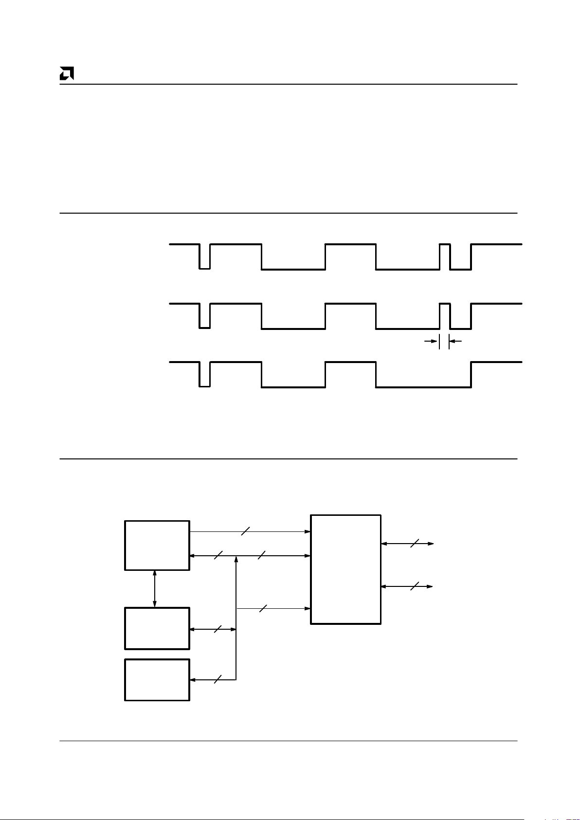
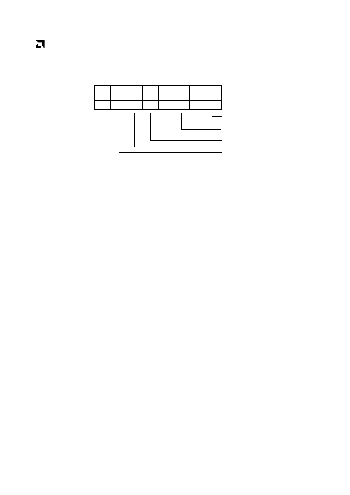
The patented GLITCH EATER Circuitry in the
Enhanced SCSI-2 Controller can be programmed to
filter glitches with widths up to 35 ns. It is designed to
dramatically increase system reliability by detecting and
removing glitches that may cause system failure. The
GLITCH EATER Circuitry is implemented on the ACK
and REQ lines since they are most susceptible to
electrical anomalies such as reflections and voltage
spikes. Such signal inconsistencies can trigger false
REQ/ACK handshaking, false data transfers, addition of
random data, and double clocking. AMD’s GLITCH
EATER Circuitry therefore maintains system performance and improves reliability. The following diagram
illustrates this circuit’s operation.
The Am53CF94 is also available in a 3.3 V version.
SCSI Environment
Device without the
GLITCH EATER Circuit
AMD’s Device with the
GLITCH EATER Circuit
GLITCH EATER Circuitry in SCSI Environment
Note:
The Glitch Window is programmable via Control Register Four (0DH), bits 6 & 7. Window may be set to 35 ns (max). Default
setting is 12 ns (single-ended).
17348B-1
Glitch Window
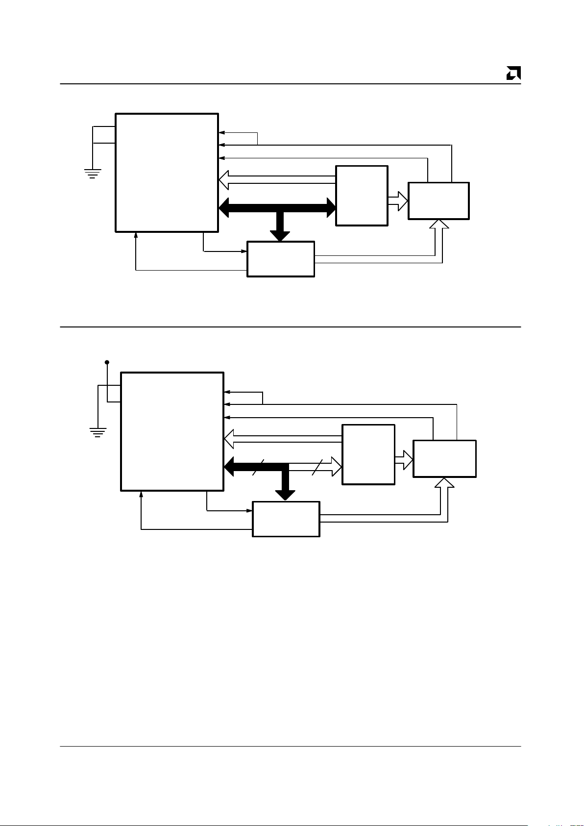
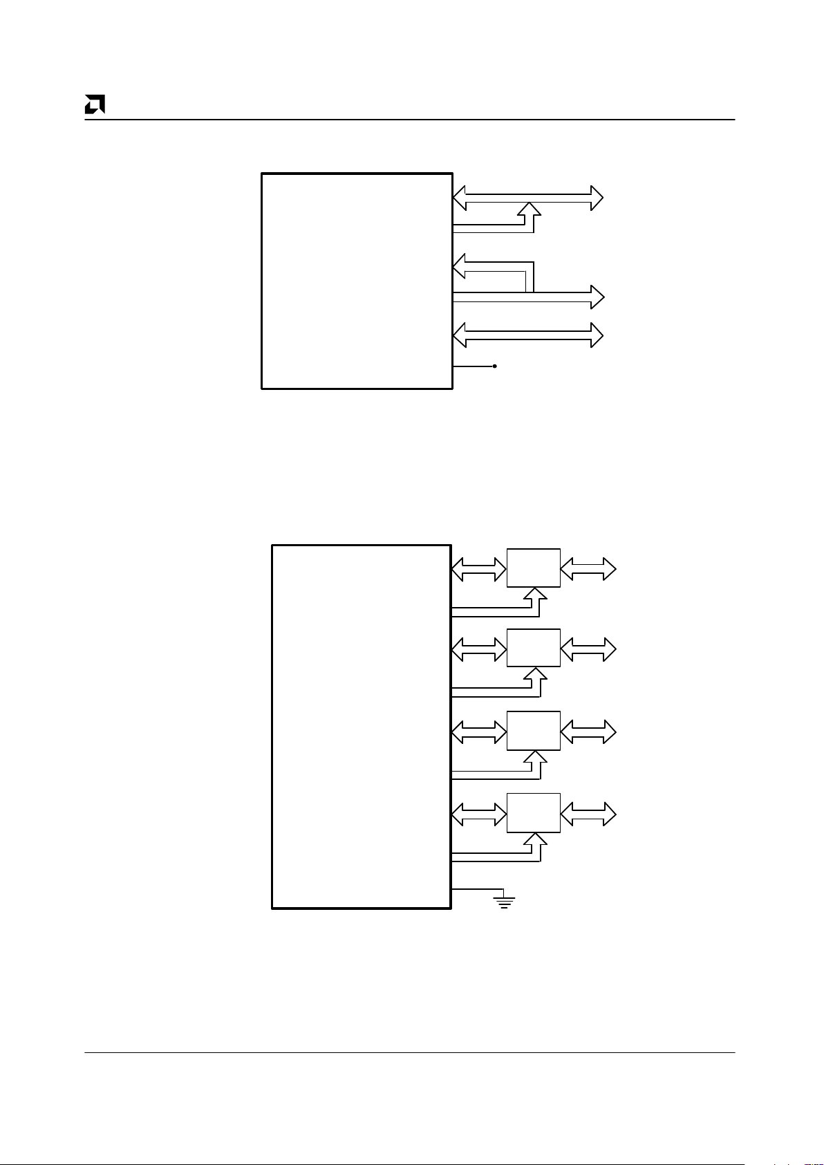
SYSTEM BLOCK DIAGRAM
9
CPU
DMA
Memory
Am53CF94/96
8
16
16
4
9
SCSI Data
16
DMA
Addr
Data
SCSI Control
16
17348B-2
Page 3
P R E L I M I N A R Y AMD
3
Am53CF94/Am53CF96
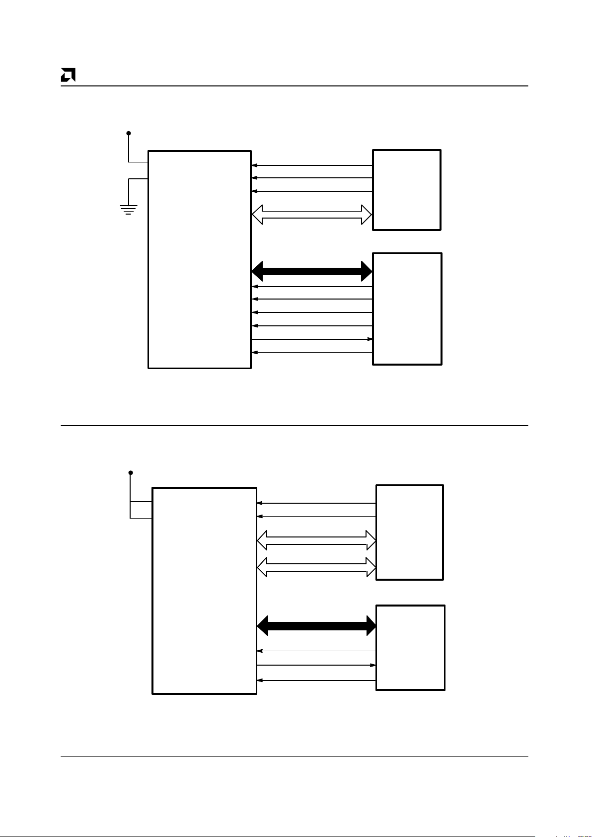
SYSTEM BUS MODE DIAGRAMS
8-Bit Data Bus
Address Bus
DMA
Controller
Host
Processor
Am53CF94/96
Bus
Controller
DMA 7–0
A 3–0
RD
WR
DMAWR
BUSMD 0
BUSMD 1
DREQ
DACK
Bus Mode 0
Single Bus Architecture: 8-Bit DMA, 8-Bit Processor
17348B-3
Data Bus
Address Bus
RD
WR
DMAWR
DREQ
DACK
DMA
Controller
Host
Processor
Am53CF94/96
Bus
Controller
DMA 15–0
A 3–0
BUSMD 0
BUSMD 1
8
16
V
DD
Bus Mode 1
Single Bus Architecture: 16-Bit DMA, 8-Bit Processor
17348B-4
Page 4
P R E L I M I N A R YAMD
4 Am53CF94/Am53CF96
SYSTEM BUS MODE DIAGRAMS
DMARD
V
DD
8-Bit Data Bus
DMA
Controller
Host
Processor
Am53CF94/96
DMA 15–0
AD 7–0
WR
DMAWR
BUSMD 0
BUSMD 1
DREQ
DACK
RD
BHE
AS0
ALE
16-Bit Data Bus
Bus Mode 2
Dual Bus Architecture: 16-Bit DMA with Byte Control,
8-Bit Multiplexed Processor Address Data
17348B-5
V
DD
Address Bus
DMA
Controller
Host
Processor
Am53CF94/96
DMA 15–0
A 3–0
WR
DMAWR
BUSMD 0
BUSMD 1
DREQ
DACK
RD
16-Bit Data Bus
8-Bit Data Bus
AD 7–0
Bus Mode 3
Dual Bus Architecture: 16-Bit DMA,
8-Bit Processor
17348B-6
Page 5
P R E L I M I N A R Y AMD
5
Am53CF94/Am53CF96
BLOCK DIAGRAM
17348B-7
Bus Interface Unit
18
18
16 x 9 FIFO
(including parity)
Parity Logic
Data Tranceivers
SCSI Control
MUX
8
8
8
9
CLK
6
4
DMA
15-0
DMAP
1-0
DMA Control
AD
7-0
Host Control
BUSMD
1-0
RESET
CS
9
SCSI Control
SCSI Bus
Data + Parity
(Single Ended)
Main
Sequencer
SCSI
Sequencer
Register
Bank
DFMODE
9
SCSI Bus
Data + Parity
Direction Control
7
SCSI Control
Direction Control
Page 6
P R E L I M I N A R YAMD
6 Am53CF94/Am53CF96
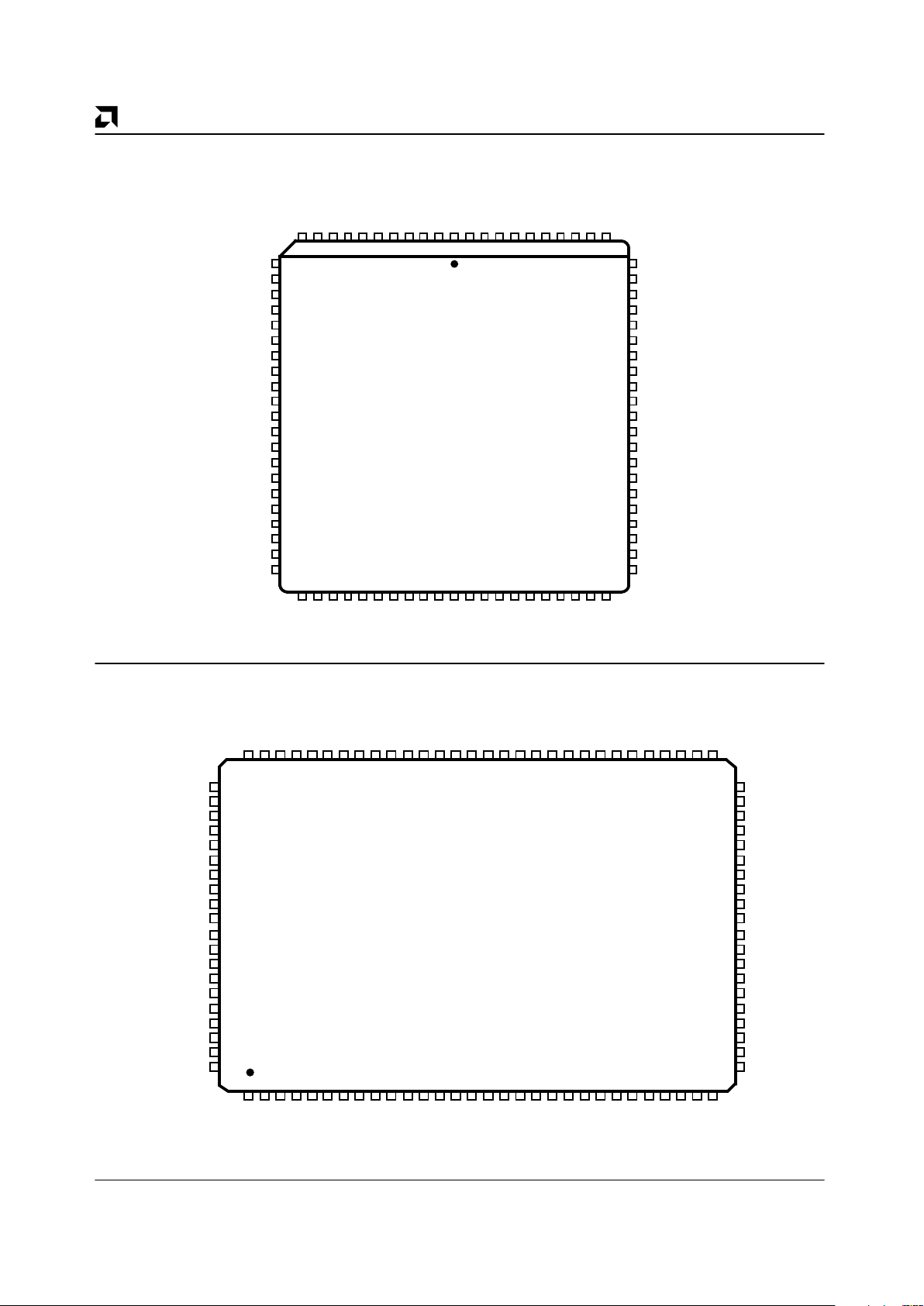
CONNECTION DIAGRAMS
Top View
17348B-8
DMA11
DMA10
DMA9
DMA8
DMA7
DMA3
DMA2
DMA1
DMA0
DMA4
DMAP0
DMAP1
DMA14
DMA13
DMA12
DMA15
DMA5
DMA6
AD3
AD2
AD1
AD0
CLK
ALE [A3]
DMARD [A2]
BHE [A1]
AS0 [A0]
AD4
AD5
DREQ
DACK
DMAWR
AD6
AD7
CS
RD
WR
BSYC
REQC
MSG
C/D
I/O
ATN
RSTC
SEL
BSY
REQ
ACK
RST
BUSMD 0
INT
RESET
SELC
BUSMD 1
ACKC
12
13
14
15
16
17
18
19
20
21
22
23
24
25
26
27
28
29
30
31
32
74
73
72
71
70
69
68
67
66
65
64
63
62
61
59
58
57
56
55
54
60
33 34 35 36 37 38 39 40 41 42 43 44 45 46 47 48 49 50 51 52 53
111098765432184838281807978777675
Am53CF94
84-Pin PLCC
SD6
SD7
SDP
V
DD
VSS
V
SS
SD3
SD4
SD5
SD0
SD1
SD2
SDC3
SDC0
SDC1
SDC2
SDC6
SDC7
SDCP
SDC4
SDC5
V
DD
V
SS
V
SS
V
SS
V
SS
V
SS
V
SS
V
SS
NC
ISEL
TSEL
DMA0
DMA1
DMA2
DMA3
DMA4
DMA5
DMA6
DMA7
DMAP0
DMA8
DMA9
DMA10
DMA11
DMA12
DMA13
DMA14
DMA15
DMAP1
NC
SD 0
SD 1
DACK
DMAWR
NC
SDC 7
SDC P
BUSMD 0
BUSMD 1
RST
ACK
REQ
SEL
ATN
I/O
C/D
MSG
ACKC
REQC
BSYC
V
SS
RSTC
BSY
RD
NC
RESET
INT
WR
SELC
V
SS
NC
SDC 6
CS
AS0 [A0]
BHE [A1]
DMARD [A2]
ALE [A3]
CLK
DFMODE
NC
AD0
AD1
AD2
AD3
V
SS
V
SS
AD4
AD5
AD6
AD7
DREQ
V
SS
V
SS
V
SS
V
SS
V
SS
V
SS
V
DD
V
DD
SDC 0
SDC 1
SDC 2
SDC 3
SDC 4
SDC 5
SD 2
SD 3
VSSV
SS
SD 4
SD 5
SD 6
SD 7
SD P
VSSV
SS
31
32
33
34
35
36
37
38
39
40
41
42
43
45
46
47
48
49
50
44
Am53CF96
100-Pin PQFP
100
99
98
97
96
95
94
93
92
91
90
89
88
87
86
85
84
83
82
81
29
1
23 45678910111213141516171819202122232425262728
30
52
80 79 78 77 76 75 74 73 72 71 70 69 68 67 66 65 64 63 62 61 60 59 58 57 56 55 54 53
51
VSSV
SS
17348B-9
Page 7
P R E L I M I N A R Y AMD
7
Am53CF94/Am53CF96
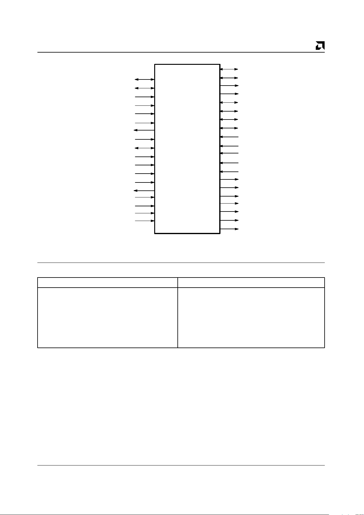
LOGIC SYMBOL
SDC P
BUSMD 1–0
*DFMODE
INT
CS
WR
RD
Am53CF94/96
SD 7–0
SD P
BSYC
MSG
C/D
I/O
ATN
SELC
RSTC
REQC
ACKC
SDC 7–0
BSY
SEL
RST
REQ
ACK
*ISEL
*TSEL
DMA 15–0
DMAP 1–0
DREQ
BHE [A1]
AS0 [A0]
ALE [A3]
AD 7–0
DMARD [A2]
DACK
DMAWR
CLK
RESET
Note:
*Pins available on the Am53CF96 only.
17348B-10
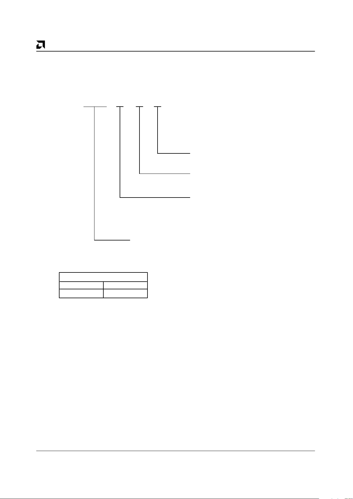
RELATED AMD PRODUCTS
Part Number Description
85C30 Enhanced Serial Communication
Controller
26LSXX Line Drivers/Receivers
33C93A Enhanced CMOS SCSI Bus
Interface Controller
80C186 Highly Integrated 16-Bit
Microprocessor
80C286 High-Performance 16-Bit
80286 Microprocessor
Part Number Description
Am386
TM
High-Performance 32-Bit
Microprocessor
53C80A SCSI Bus Controller
80188 Highly Integrated 8-Bit Microprocessor
85C80 Combination 53C80A SCSI and
85C30 ESCC
53C94LV Low Voltage, High Performance
SCSI Controller
Page 8
P R E L I M I N A R YAMD
8 Am53CF94/Am53CF96
ORDERING INFORMATION
Standard Products
AMD standard products are available in several packages and operating ranges. The order number (Valid Combination) is
formed by a combination of:
TEMPERATURE RANGE
C = Commercial
PACKAGE TYPE
J = 84-Pin PLCC (PL 084)
K = 100-Pin Metric PQFP (PQR100)
DEVICE NUMBER/DESCRIPTION
Am53CF94/Am53CF96
Enhanced SCSI-2 Controller
AM53CF94
AM53CF96
AM53CF96 K C
Valid Combinations
Valid Combinations list configurations planned to be
supported in volume for this device. Consult the local AMD sales office to confirm availability of specific
valid combinations or to check on newly released
combinations.
JC
KC, KC/W
Valid Combinations
ALTERNATE PACKAGING OPTION
/W = Trimmed and Formed in a Tray
Blank = Molded Carrier Ring (36 mm)
/W
Page 9
P R E L I M I N A R Y AMD
9
Am53CF94/Am53CF96
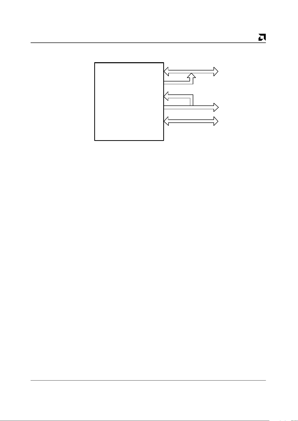
SCSI OUTPUT CONNECTIONS
Am53CF94
Am53CF94 Single Ended SCSI Bus Configuration
SDC 7–0, P
SELC, BSYC, REQC,
ACKC, RSTC
SD 7–0, P
SEL, BSY, REQ, ACK, RST
MSG, C/D, I/O, ATN
17348B-11
Page 10
P R E L I M I N A R YAMD
10 Am53CF94/Am53CF96
SCSI OUTPUT CONNECTIONS
Am53CF96
Am53CF96 Single Ended SCSI Bus Configuration
SDC 7–0, P
SELC, BSYC, REQC,
ACKC, RSTC
SD 7–0, P
SEL, BSY, REQ, ACK, RST
MSG, C/D, I/O, ATN
DFMODE
V
CC
17348B-12
SDC 7–0, P
SELC, BSYC, RSTC
SD 7–0, P
SEL, BSY, RST
MSG, C/D, I/O, REQ
DFMODE
ATN, ACK
Am53CF96 Differential SCSI Bus Configuration
TSEL
ISEL
Am53CF96
DT
DT
DT
DT
17348B-13
Page 11
P R E L I M I N A R Y AMD
11
Am53CF94/Am53CF96
TSEL
Vcc
Differential Transceiver Connections for the Differential SCSI Bus Configuration
Using 75ALS170 and 75ALS171 Transceivers
Vcc
SELC
GND
SEL
+ SEL
– SEL
BSYC
GND
BSY
+ BSY
– BSY
RSTC
GND
RST
+ RST
– RST
GND
75ALS171
SDC 6
SD 6
– SD 6
+ SD 6
SDC 7
SD 7
– SD 7
+ SD 7
SDC P
SD P
– SD P
+ SD P
75ALS170
SDC 3
SD 3
– SD 3
+ SD 3
SDC 4
SD 4
– SD 4
+ SD 4
SDC 5
SD 5
– SD 5
+ SD 5
75ALS170
SDC 0
SD 0
– SD 0
+ SD 0
SDC 1
SD 1
– SD 1
+ SD 1
SDC 2
SD 2
– SD 2
+ SD 2
75ALS170
ATN
ISEL
– ATN
+ ATN
75ALS170
– MSG
+ MSG
– C/D
TSEL
MSG
TSEL
C/D
+ C/D
TSEL
I/O
– I/O
+ I/O
75ALS170
REQC
ACKC
REQ
+ REQ
– REQ
ISEL
ACK
+ ACK
– ACK
75ALS171
GND
17348B-14
Page 12
P R E L I M I N A R YAMD
12 Am53CF94/Am53CF96
SDC 6
SD 6
Differential Transceiver Connections for the Differential
SCSI Bus Configuration Using 75176A Transceiver
– SD 6
+ SD 6
SD 6
SDC 6
RSTC
GND
RST
+ RST
– RST
GND
SDC 0
SD 0
– SD 0
+ SD 0
SDC 0
SD 0
TSEL
MSG
– MSG
+ MSG
MSG
TSEL
SDC 1
SD 1
– SD 1
+ SD 1
SD 1
SDC 1
TSEL
C/D
– C/D
+ C/D
C/D
TSEL
SDC 2
SD 2
– SD 2
+ SD 2
SD 2
SDC 2
TSEL
I/O
– I/O
+ I/O
I/O
TSEL
SDC 3
SD 3
– SD 3
+ SD 3
SD 3
SDC 3
ISEL
ATN
– ATN
+ ATN
ATN
ISEL
SDC 4
SD 4
– SD 4
+ SD 4
SD 4
SDC 4
SELC
GND
SEL
+ SEL
– SEL
GND
SDC 5
SD 5
– SD 5
+ SD 5
SD 5
SDC 5
BSYC
GND
BSY
+ BSY
– BSY
GND
SDC 7
SD 7
– SD 7
+ SD 7
SD 7
SDC 7
TSEL
REQC
REQ
+ REQ
– REQ
GND
SDC P
SD P
– SD P
+ SD P
SD P
SDC P
ISEL
ACKC
ACK
+ ACK
– ACK
GND
17348B-15
Page 13

P R E L I M I N A R Y AMD
13
Am53CF94/Am53CF96
PIN DESCRIPTION
Host Interface Signals
DMA 15–0
Data/DMA Bus
(Input/Output, Active High, Internal Pull-up)
The configuration of this bus depends on the Bus Mode
1–0 (BUSMD 1–0) inputs. When the device is configured for single bus operation, the host can access the
internal register set on the lower eight lines while DMA
accesses can be made to the FIFO using the entire bus.
When using the Byte Mode via the BHE and A0 inputs
the data can be transferred on either the upper or lower
half of the DMA 15–0 bus.
DMAP 1–0
Data/DMA Parity Bus
(Input/Output, Active High, Internal Pull-up)
These lines are odd parity for the DMA 15–0 bus. DMAP
1 is the parity for the upper half of the bus (DMA 15–8)
and DMAP 0 is the parity for the lower half of the bus
(DMA 7–0).
ALE [A3]
Address Latch Enable [Address 3]
(Input, Active High)
This is a dual function input. When the device is configured for the dual bus mode (two buses, multiplexed and
byte control), this input acts as ALE. As ALE, this input
latches the address on the AD 7–0 bus on its low going
edge. When the device is configured for all other bus
modes, this input acts as A3. As A3, this input is the third
bit of the address bus.
DMARD [A2]
DMA Read [Address 2]
(Input, Active Low [Active High])
This is a dual function input. When the device is configured for the dual bus mode (two buses, multiplexed and
byte control), this input acts as DMARD. As DMARD,
this input is the read signal for the DMA 15–0 bus. When
the device is configured for all other bus modes, this input acts as A2. As A2, this input is the second bit of the
address bus.
BHE [A1]
Bus High Enable [Address 1]
(Input, Active High)
This is a dual function input. When the device is configured for the dual bus mode (two buses, multiplexed and
byte control), this input acts as BHE. As BHE, this input
works in conjunction with AS0 to indicate the lines on
which data transfer will take place. When the device is
configured for all other bus modes this input acts as A1.
As A1, this input is the first bit of the address bus.
AS0 [A0]
Address Status [Address 0]
(Input, Active High)
This is a dual function input. When the device is configured for the dual bus mode (two buses, multiplexed and
byte control), this input acts as AS0. As AS0, this input
works in conjunction with BHE to indicate the lines on
which data transfer will take place. When the device is
configured for all other bus modes, this input acts as A0.
As A0, this input is the zeroth bit of the address bus.
The following is the decoding for the BHE and AS0
inputs:
BHE AS0 Bus Used
1 1 Upper Bus – DMA 15–8, DMAP 1
1 0 Full Bus – DMA 15–0, DMAP 1–0
0 1 Reserved
0 0 Lower Bus – DMA 7–0, DMAP 0
DREQ
DMA Request
(Output, Active High, Hi-Z)
This output signal to the DMA controller will be active
during DMA read and write cycles. During a DMA read
cycle it will be active as long as there is a word (or a byte
in the byte mode) in the FIFO to be transferred to memory. During a DMA write cycle it will be active as long as
there is an empty space for a word (or a byte in mode 2)
in the FIFO.
DACK
DMA Acknowledge
(Input, Active Low)
This input signal from the DMA controller will be active
during DMA read and write cycles. The DACK signal is
used to access the DMA FIFO only and should never be
active simultaneously with the CS signal, which accesses the registers only.
AD 7–0
Host Address Data Bus
(Input/Output, Active High, Internal Pull-up)
This bus is used only in the dual bus mode. This bus allows the host processor to access the device’s internal
registers while the DMA bus is transferring data. When
using multiplexed bus, these lines can be used for address and data. When using non multiplexed bus these
lines can be used for the data only.
Page 14

P R E L I M I N A R YAMD
14 Am53CF94/Am53CF96
DMAWR
DMA Write
(Input, Active Low)
This signal writes the data onto the DMA 15–0 and
DMAP 1–0 bus into the internal FIFO when DACK is
also active. When in the single bus mode this signal
must be tied to the WR signal.
RD
Read
(Input Active Low)
This signal reads the internal device registers and
places their contents on the data bus, when either CS
signal or DACK signal is active.
WR
Write
(Input Active Low)
This signal writes the internal device registers with the
value present on the (AD 7–0 bus or the DMA 15–0 and
DMAP 1–0 bus), when the CS signal is also active.
CS
Chip Select
(Input Active Low)
This signal enables the read and write of the device registers. CS enables access to any register (including the
FIFO) while the DACK enables access only to the FIFO.
CS and DACK should never be active simultaneously in
the single bus mode, they may however be active simultaneously in the dual bus mode provided the CS signal is
not enabling access to the FIFO.
INT
Interrupt
(Output, Active Low, Open Drain)
This signal is a non-maskable interrupt flag to the host
processor. This signal is latched on the output on the
high going edge of the clock. This flag may be cleared by
reading the Interrupt Status Register (ISTAT) or by performing a device reset (hard or soft). This flag is not
cleared by a SCSI reset.
DFMODE
Differential Mode
(Input, Active Low)
This input is available only on the Am53CF96. This input
configures the SCSI bus to either single ended or differential mode. When this input is active, the device operates in the differential SCSI mode. The SCSI data is
available on the SD 7–0 lines and the high active transceiver enables on the SDC 7–0 outputs. When this input
is inactive, the device operates in the single ended SCSI
mode. The SCSI input data is available on SD 7–0 lines
and the output data is available on SDC 7–0 lines. In the
single ended SCSI mode, the SD 7–0 and the SDC 7–0
buses can be tied together externally.
BUSMD 1–0
Bus Mode
(Input, Active High)
These inputs configure the device for single bus or dual
bus operation and the DMA bus width.
BUSMD1 BUSMD0 Bus Configuration
1 1 Two buses: 8-bit Host Bus
and 16-bit DMA Bus
Register Address on A 3–0
and Data on AD Bus
1 0 Two buses: Multiplexed
and byte control
Register Address on AD 3–0
and Data on AD Bus
0 1 Single bus: 8-bit Host Bus
and 16-bit DMA Bus
Register Address on A 3–0
and Data on DMA Bus
0 0 Single bus: 8-bit Host Bus
and 8-bit DMA Bus
Register Address on A 3–0
and Data on DMA Bus
CLK
Clock
(Input)
Clock input used to generate all the internal device timings. The maximum frequency of this input is 40 MHz.
and a minimum of 10 MHz to maintain the SCSI bus
timings.
RESET
Reset
(Input, Active High)
This input when active resets the device. The RESET input must be active for at least two CLK periods after the
voltage on the power inputs have reached Vcc
minimum.
SCSI Interface Signals
SD 7–0
SCSI Data
(Input/Output, Active Low, Schmitt Trigger)
When the device is configured in the Single Ended SCSI
Mode (DFMODE inactive) these pins are defined as inputs for the SCSI data bus. When the device is configured in the Differential SCSI Mode (DFMODE active)
these pins are defined as bidirectional SCSI data bus.
Page 15

P R E L I M I N A R Y AMD
15
Am53CF94/Am53CF96
SD P
SCSI Data Parity
(Input/Output, Active Low, Schmitt Trigger)
When the device is configured in the Single Ended SCSI
Mode (DFMODE inactive) this pin is defined as the input
for the SCSI data parity. When the device is configured
in the Differential SCSI Mode (DFMODE active) this pin
is defined as bidirectional SCSI data parity.
SDC 7–0
SCSI Data Control
(Output, Active Low, Open Drain)
When the device is configured in the Single Ended SCSI
Mode (DFMODE inactive) these pins are defined as outputs for the SCSI data bus. When the device is configured in the Differential SCSI Mode (DFMODE active)
these pins are defined as direction controls for the external differential transceivers. In this mode, a signal high
state corresponds to an output to the SCSI bus and a
low state corresponds to an input from the SCSI bus.
SDC P
SCSI Data Control Parity
(Output, Active Low, Open Drain)
When the device is configured in the Single Ended SCSI
Mode (DFMODE inactive) this pin is defined as an output for the SCSI data parity. When the device is configured in the Differential SCSI Mode (DFMODE active)
this pin is defined as the direction control for the external
differential transceiver. In this mode, a signal high state
corresponds to an output to the SCSI bus and a low
state corresponds to an input from the SCSI bus.
MSG
Message
(Input/Output, Active Low, Schmitt Trigger)
This is a bidirectional signal with 48 mA output driver.
It is an output in the Target mode and a Schmitt trigger
input in the Initiator mode.
C/D
Command/Data
(Input/Output, Schmitt Trigger)
This is a bidirectional signal with 48 mA output driver.
It is an output in the Target mode and a Schmitt trigger
input in the Initiator mode.
I/O
Input/Output
(Input/Output, Schmitt Trigger)
This is a bidirectional signal with 48 mA output driver.
It is an output in the Target mode and a Schmitt trigger
input in the Initiator mode.
ATN
Attention
(Input/Output, Active Low, Schmitt Trigger)
This signal is a 48 mA output in the Initiator mode and a
Schmitt trigger input in the Target mode. This signal will
be asserted when the Initiator detects a parity error or it
can be asserted via certain Initiator commands.
BSY
Busy
(Input, Active Low, Schmitt Trigger)
This is a SCSI input signal with a Schmitt trigger.
SEL
Select
(Input, Active Low, Schmitt Trigger)
This is a SCSI input signal with a Schmitt trigger.
RST
Reset
(Input, Active Low, Schmitt Trigger)
This is a SCSI input signal with a Schmitt trigger.
REQ
Request
(Input, Active Low, Schmitt Trigger)
This is a SCSI input signal with a Schmitt trigger.
ACK
Acknowledge
(Input, Active Low, Schmitt Trigger)
This is a SCSI input signal with a Schmitt trigger.
BSYC
Busy Control
(Output, Active Low, Open Drain)
This is a SCSI output with 48 mA drive. When the device
is configured in the Single Ended SCSI Mode (DFMODE
inactive) this pin is defined as a BSY output for the SCSI
bus. When the device is configured in the Differential
SCSI Mode (DFMODE active) this pin is defined as the
direction control for the external differential transceiver.
In this mode, a signal high state corresponds to an output to the SCSI bus and a low state corresponds to an
input from the SCSI bus.
SELC
Select Control
(Output, Active Low, Open Drain)
This is a SCSI output with 48 mA drive. When the device
is configured in the Single Ended SCSI Mode (DFMODE
inactive) this pin is defined as a SEL output for the SCSI
bus. When the device is configured in the Differential
SCSI Mode (DFMODE active) this pin is defined as the
direction control for the external differential transceiver.
In this mode, a signal high state corresponds to an output to the SCSI bus and a low state corresponds to an
input from the SCSI bus.
Page 16

P R E L I M I N A R YAMD
16 Am53CF94/Am53CF96
RSTC
Reset Control
(Output, Active Low, Open Drain)
This is a SCSI output with 48 mA drive. The Reset SCSI
command will cause the device to drive RSTC active for
25 ms–40 ms, which will depend on the CLK frequency
and the conversion factor. When the device is configured in the Single Ended SCSI Mode (DFMODE inactive) this pin is defined as a RST output for the SCSI bus.
When the device is configured in the Differential SCSI
Mode (DFMODE active) this pin is defined as the direction control for the external differential transceiver. In
this mode, a signal high state corresponds to an output
to the SCSI bus and a low state corresponds to an input
from the SCSI bus.
REQC
Request Control
(Output, Active Low, Open Drain)
This is a SCSI output with 48 mA drive. This signal is
activated only in the Target mode.
ACKC
Acknowledge Control
(Output, Active Low, Open Drain)
This is a SCSI output with 48 mA drive. This signal is activated only in the Initiator mode.
ISEL
Initiator Select
(Output, Active High)
This signal is available on the Am53CF96 only. This signal is active whenever the device is in the Initiator mode.
In the differential mode this signal is used to enable the
Initiator signals ACKC and ATN and the device also
drives these signals.
TSEL
Target Select
(Output, Active High)
This signal is available on the Am53CF96 only. This signal is active whenever the device is in the Target mode.
In the differential mode this signal is used to enable the
Target signals REQC, MSG, C/D and I/O and the device
also drives these signals.
FUNCTIONAL DESCRIPTION
Register Map
Address
(Hex.) Operation Register
00 Read Current Transfer Count
Register Low
00 Write Start Transfer Count Register
Low
01 Read Current Transfer Count
Register Middle
01 Write Start Transfer Count Register
Middle
02 Read/Write FIFO Register
03 Read/Write Command Register
04 Read Status Register
04 Write SCSI Destination ID Register
05 Read Interrupt Status Register
05 Write SCSI Timeout Register
06 Read Internal State Register
06 Write Synchronous Transfer Period
Register
Address
(Hex.) Operation Register
07 Read Current FIFO/Internal State
Register
07 Write Synchronous Offset Register
08 Read/Write Control Register 1
09 Write Clock Factor Register
0A Write Forced Test Mode Register
0B Read/Write Control Register 2
0C Read/Write Control Register 3
0D Read/Write Control Register 4
0E Read Current Transfer Count
Register High
0E Write Start Transfer Count
Register High
0F Write Data Alignment Register
Note:
Not all registers in this device are both readable and writable. Some read only registers share the same address with write only
registers. The registers can be accessed by asserting the
CS
signal and then asserting either
RD
or WR signal depending on the
operation to be performed. Only the FIFO Register can be accessed by asserting either
CS
or
DACK
in conjunction with RD and
WR
signals or
DMARD
and
DMAWR
signals. The register address inputs are ignored when
DACK
is used but must be valid
when
CS
is used.
Page 17
P R E L I M I N A R Y AMD
17
Am53CF94/Am53CF96
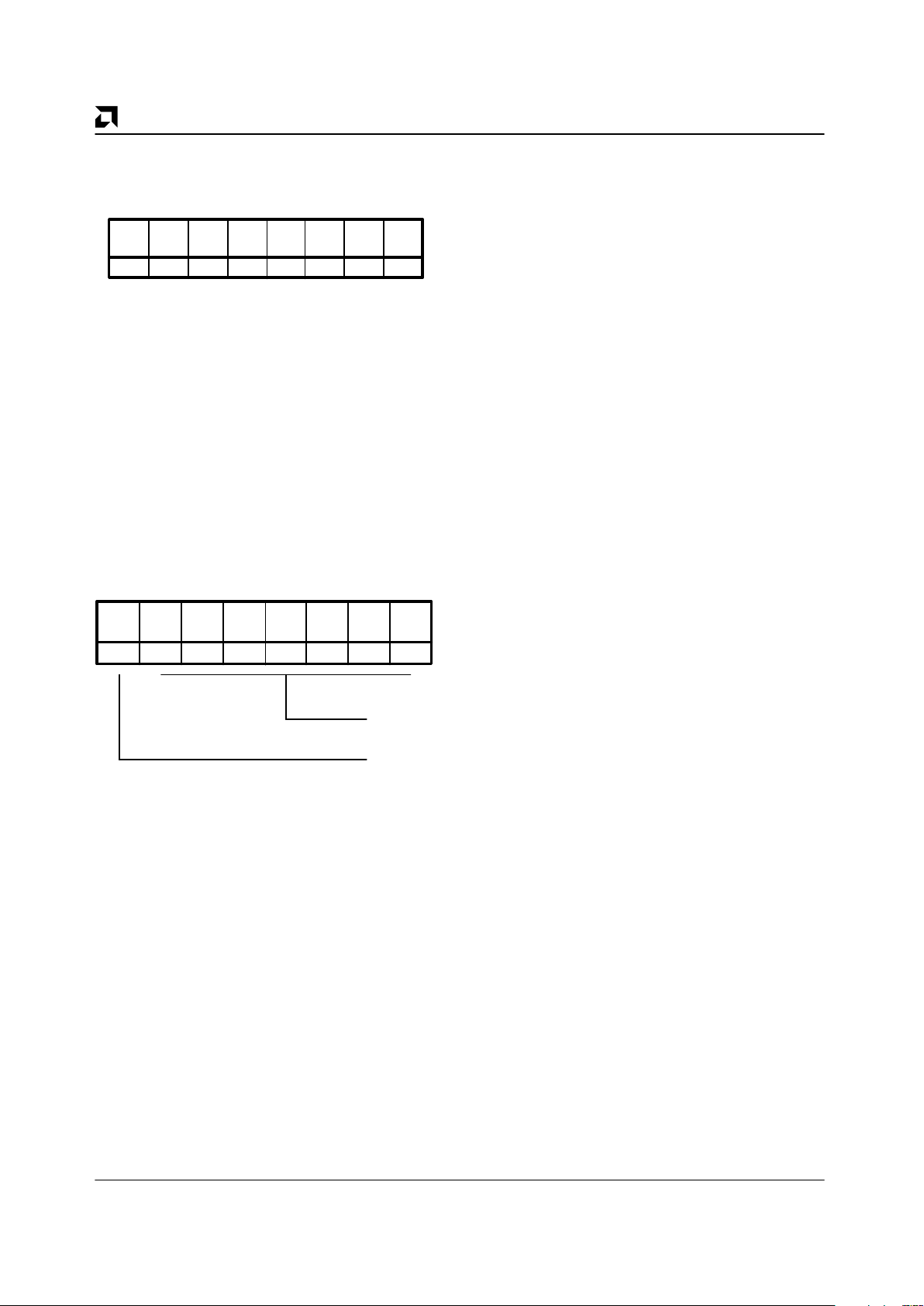
Current Transfer Count Register
(00H, 01H, 0EH) Read Only
Current Transfer Count Register
CTCREG
Address: 00H, 01H, 0EH
Type: Read
15 14 13 12 11 10 9 8
CRVL15 CRVL14 CRVL13 CRVL12 CRVL11 CRVL10 CRVL9 CRVL8
xxxxxxxx
76543210
CRVL7 CRVL6 CRVL5 CRVL4 CRVL3 CRVL2 CRVL1 CRVL0
xxxxxxxx
23 22 21 20 19 18 17 16
CRVL23 CRVL22 CRVL21 CRVL20 CRVL19 CRVL18 CRVL17 CRVL16
xxxxxxxx
17348B-16
CTCREG – Bits 23:0 – CRVL 23:0 – Current
Value 23:0
This is a three-byte register which decrements to keep
track of the number of bytes transferred during a DMA
transfer. Reading these registers returns the current
value of the counter. The counter will decrement by one
for every byte and by two for every word transferred. The
transaction is complete when the count reaches zero,
and bit 4 of the Status Register (04H) is set. Should the
sequence terminate early, the sum of the values in the
Current FIFO (07H) and the Current Transfer Count
Register reflect the number of bytes remaining.
The least significant byte is located at address 00H, the
middle byte is located at address 01H, and the most significant byte is located at address 0EH. Register 0EH
extends the total width of the register from 16 to 24
bits, and is only enabled when the Enable Features
bit (bit 6) of Control Register Two is set to a value
of ‘1’.
These registers are automatically loaded with the values in the Start Transfer Count Register every time a
DMA command is issued. However, following a chip or
power on reset, up until the time register 0EH is loaded,
the Am53CF94/96’s part-unique ID can be obtained by
reading register 0EH.
In the Target mode, this counter is decremented by the
active edge of DACK during the Data-In phase and by
REQC during the Data-Out phase.
In the Initiator mode, the counter is decremented by the
active edge of DACK during the Synchronous Data-In
phase or by ACKC during the Asynchronous Data-In
phase and by DACK during the Data-Out phase.
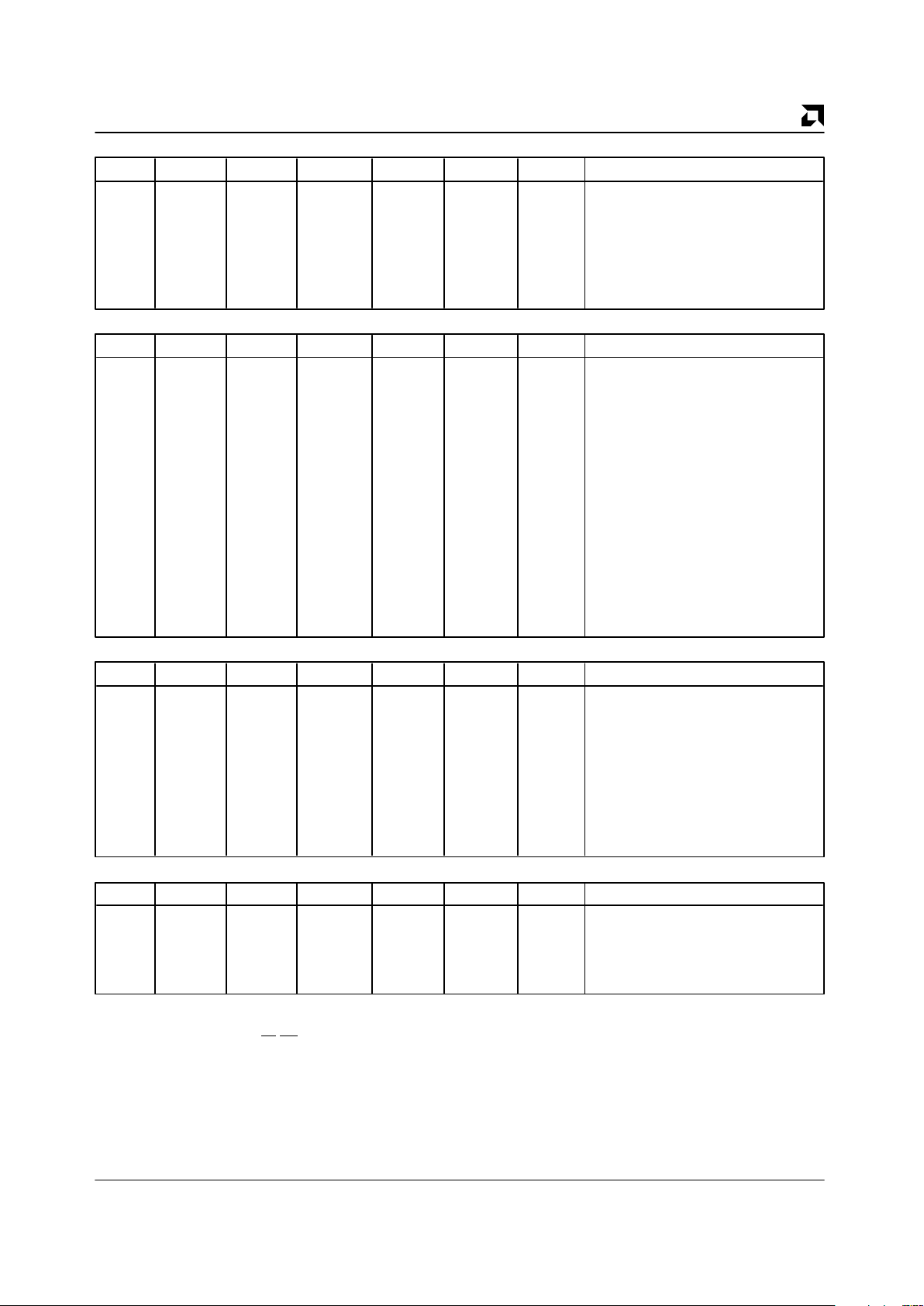
Start Transfer Count Register
(00H, 01H, 0EH) Write Only
Start Transfer Count Register
STCREG
Address: 00H–01H
Type: Write
15 14 13 12 11 10 9 8
STVL15 STVL14 STVL13 STVL12 STVL11 STVL10 STVL9 STVL8
xxxxxxxx
76543210
STVL7 STVL6 STVL5 STVL4 STVL3 STVL2 STVL1 STVL0
xxxxxxxx
23 22 21 20 19 18 17 16
STVL23 STVL22 STVL21 STVL20 STVL19 STVL18 STVL17 STVL16
xxxxxxxx
17348B-17
STCREG – Bits 15:0 – STVL 15:0 – Start Value 15:0
This is a three-byte register which contains the number
of bytes to be transferred during a DMA operation. The
value in the Start Transfer Count Register must be programmed prior to command execution.
The least significant byte is located at address 00H, the
middle byte is located at address 01H, and the most significant byte is located at address 0EH. Register 0EH
extends the total width of the register from 16 to 24 bits,
and is only enabled when the Enable Features bit (bit 6)
of Control Register Two is set to a value of ‘1’. This sets
the maximum transfer count to 16.78 MBytes. When a
value of ‘0’ is written to these registers, the transfer
count will be set to the maximum. A DMA NOP command must be issued before the transfer counter values
can be written to 00H, 01H, and 0EH.
These registers retain their value until overwritten, and
are therefore unaffected by a hardware or software reset. This reduces programming redundancy since it is
no longer necessary to reprogram the count for subsequent DMA transfers of the same size.
Page 18
P R E L I M I N A R YAMD
18 Am53CF94/Am53CF96
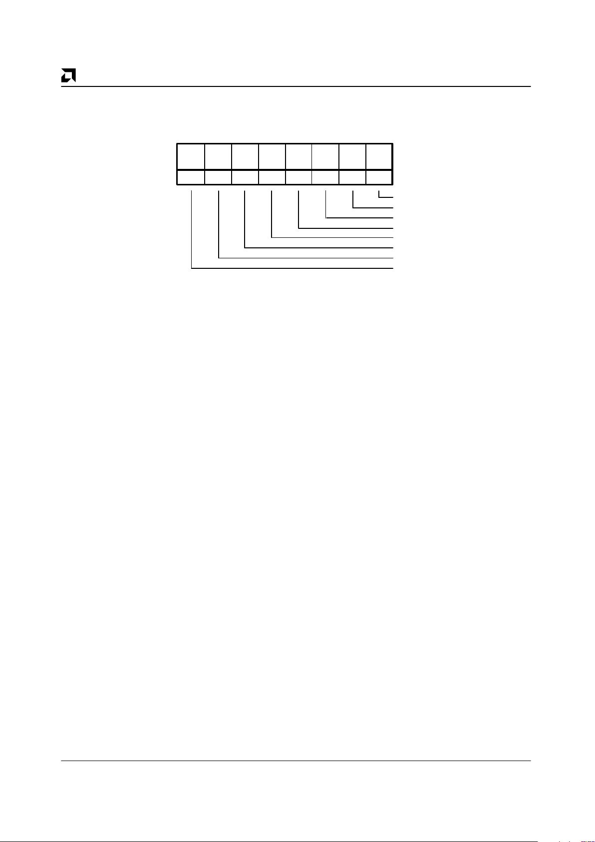
FIFO Register (02H) Read/Write
FIFO Register
FFREG
Address: 02H
Type: Read/Write
76543210
FF7 FF6 FF5 FF4 FF3 FF2 FF1 FF0
00000000
17348B-18
FFREG – Bits 7:0 – FF 7:0 – FIFO 7:0
The FIFO on the Am53CF94/96 is 16 bytes deep and is
used to transfer SCSI data to and from the ESC. The
bottom of the FIFO may be accessed via a read or write
to this register. This is the only register that can also be
accessed by DACK along with DMARD or DMAWR or
with REQ or ACK. This register is reset to zero by hardware or software reset, or at the start of a selection or
reselection sequence, or if Clear FIFO command is
issued.
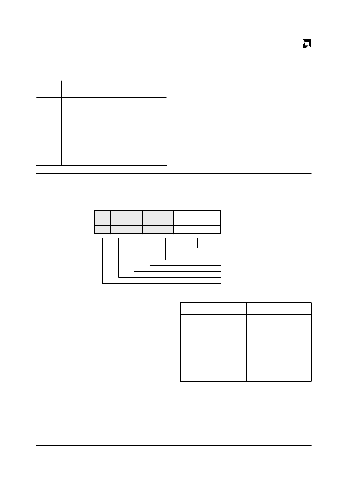
Command Register (03H) Read/Write
Command Register
CMDREG
Address: 03H
Type: Read/Write
76543210
DMA CMD6 CMD5 CMD4 CMD3 CMD2 CMD1 CMD0
xxxxxxxx
Command 6:0
Direct Memory
Access
17348B-19
Commands to the ESC are issued by writing to this register which is two bytes deep. Commands may be
queued, and will be read from the bottom of the queue.
At the completion of the bottom command, the top command, if present, will drop to the bottom of the register to
begin execution. All commands are executed within six
clock cycles of dropping to the bottom of the Command
Register, with the exception of the Reset SCSI Bus, Reset Device, and DMA Stop commands. These commands are not queued and are executed within four
clock cycles of being loaded into the top this register.
Interrupts are sometimes generated upon command
completion. Should both commands generate interrupts, and the first interrupt has not been serviced, the
interrupt from the second (top) command will be stacked
behind the first. The Status Register, Interrupt Register,
and Internal State Register will be updated to apply to
the second interrupt after the microprocessor services
the first interrupt.
Reading this register will return the command currently
being executed (or the last command executed if there
are no pending commands). When this register is
cleared, existing commands will be terminated and any
queued commands will be ignored. However, it does not
reset the register bits to ‘00H’.
CMDREG – Bit 7 – DMA – Direct Memory Access
When set, this bit notifies the device that the command
is a DMA instruction, when reset it is a non-DMA instruction. For DMA instructions the Current Transfer Count
Register (CTCREG) will be loaded with the contents of
the Start Transfer Count Register (STCREG). The data
is then transferred and the CTCREG is decremented for
each byte until it reaches zero.
CMDREG – Bits 6:0 – CMD 6:0 – Command 6:0
These command bits decode the commands that the
device needs to perform. There are a total of 31 commands grouped into four categories. The groups are
Initiator Commands, Target Commands, Selection/
Reselection Commands and General Purpose Commands.
Page 19
P R E L I M I N A R Y AMD
19
Am53CF94/Am53CF96
Initiator Commands
CMD6 CMD5 CMD4 CMD3 CMD2 CMD1 CMD0 Command
0010000Information Transfer
00100 01Initiator Command Complete Steps
0010010Message Accepted
0011000Transfer Pad Bytes
0011010*Set ATN
0011011*Reset ATN
CMD6 CMD5 CMD4 CMD3 CMD2 CMD1 CMD0 Command
0100000Send Message
0100001Send Status
0100010Send Data
0100011Disconnect Steps
0100100Terminate Steps
0100101Target Command Complete Steps
0100111*Disconnect
0101000Receive Message Steps
0101001Receive Command
0101010Receive Data
0101011Receive Command Steps
0000100*DMA Stop
0000101Access FIFO Command
Idle Commands
CMD6 CMD5 CMD4 CMD3 CMD2 CMD1 CMD0 Command
1000000Reselect Steps
10000 01Select without ATN Steps
1000010Select with ATN Steps
1000011Select with ATN and Stop Steps
1000100*Enable Selection/Reselection
1000101Disable Selection/Reselection
1000110Select with ATN3 Steps
1000111Reselect with ATN3 Steps
General Commands
CMD6 CMD5 CMD4 CMD3 CMD2 CMD1 CMD0 Command
0000000*No Operation
00000 01*Clear FIFO
0000010*Reset Device
0000011Reset SCSI Bus
Target Commands
Note:
*Denotes commands which do
not generate interrupts upon completion.
Page 20
P R E L I M I N A R YAMD
20 Am53CF94/Am53CF96
Status Register (04H) Read
Status Register
STATREG
Address: 04H
Type: Read
76543210
INT IOE PE CTZ GCV MSG C/D I/O
0000 0 xxx
Illegal Operation Error
Parity Error
Count to Zero
Group Code Valid
Message
Command/Data
Input/Output
Interrupt
17348B-20
This read only register contains flags to indicate the
status and phase of the SCSI transactions. It indicates
whether an interrupt or error condition exists. It should
be read every time the host is interrupted to determine
which device is asserting an interrupt. If the ENF bit is
set (CNTLREG2, bit 6), the SCSI bus phase of the last
complete command (preceding the interrupt) will be
latched until the Interrupt Status Register (INSTREG) is
read. If the ENF bit is disabled, this register will reflect
the current bus phase. If command stacking is used, two
interrupts might occur. Reading this register will clear
the status information for the first interrupt and update
the Status Register for the second interrupt.
STATREG – Bit 7 – INT – Interrupt
The INT bit is set when the device asserts the interrupt
output. This bit will be cleared by a hardware or software
reset. Reading the Interrupt Status Register (INSTREG)
will deassert the interrupt output and also clear this bit.
STATREG – Bit 6 – IOE – Illegal Operation Error
The IOE bit is set when an illegal operation is attempted.
This condition will not cause an interrupt, it will be detected by reading the Status Register (STATREG) while
servicing another interrupt. The following conditions will
cause the IOE bit to be set:
■ DMA and SCSI transfer directions are opposite.
■ FIFO overflows or data is overwritten.
■ In Initiator mode an unexpected phase change
detected during synchronous data transfer.
■ Command Register overwritten.
This bit will be cleared by reading the Interrupt Status
Register (INSTREG) or by a hard or soft reset.
STATREG – Bit 5 – PE – Parity Error
The PE bit is set if any of the parity checking options are
enabled and the device detects a parity error on bytes
sent or received on the SCSI Bus. Parity options are
controlled by bits 5:4 in Control Register One
(CNTLREG1), and by bits 2:0 in Control Register Two
(CNTLREG2). The combination of enabled options will
determine if parity is generated from the data bytes
internally by the chip, or if it is passed between buffer
and SCSI Bus without being altered. Detection of a
parity error condition will not cause an interrupt but will
be reported with other interrupt causing conditions.
This bit will be cleared by reading the Interrupt Status
Register (INSTREG) or by a hard or soft reset.
STATREG – Bit 4 – CTZ – Count To Zero
The CTZ bit is set when the Current Transfer Count
Register (CTCREG) has counted down to zero. This bit
will be reset when the CTCREG is written with a nonzero value.
Reading the Interrupt Status Register (INSTREG) will
not affect this bit. This bit will however be cleared by a
hard or soft reset.
Note:
A non-DMA NOP will not reset the CTZ bit since it does
not load the CTCREG. However, a DMA NOP will reset
this bit since it loads the CTCREG.
STATREG – Bit 3 – GCV – Group Code Valid
The GCV bit is set if the group code field in the Command Descriptor Block (CDB) is one that is defined by
the ANSI Committee in their document X3.131 – 1986. If
the SCSI-2 Feature Enable (S2FE) bit in the Control
Register 2 (CNTLREG2) is set, Group 2 commands will
be treated as ten byte commands and the GCV bit will be
set. If S2FE is reset then Group 2 commands will be
treated as reserved commands. Group 3 and 4 commands will always be considered reserved commands.
The device will treat all reserved commands as six byte
commands. Group 6 commands will always be treated
as vendor unique six byte commands and Group 7 commands will always be treated as vendor unique ten byte
commands.
The GCV bit is cleared by reading the Interrupt Status
Register (INSTREG) or by a hard or soft reset.
Page 21
P R E L I M I N A R Y AMD
21
Am53CF94/Am53CF96
STATREG – Bit 2 – MSG – Message
STATREG – Bit 1 – C/D – Command/Data
STATREG – Bit 0 – I/O – Input/Output
Bit2 Bit1 Bit0
MSG C/D I/O SCSI Phase
1 1 1 Message In
1 1 0 Message Out
1 0 1 Reserved
1 0 0 Reserved
0 1 1 Status
0 1 0 Command
0 0 1 Data_In
0 0 0 Data_Out
The MSG, C/D and I/O bits together can be referred to
as the SCSI Phase bits. They indicate the phase of the
SCSI bus. These bits may be latched or unlatched
depending on whether or not the ENF bit in Control
Register Two is set.
In the latched mode the SCSI phase bits are latched at
the end of a command and the latch is opened when the
Interrupt Status Register (INSTREG) is read. In the unlatched mode, they indicate the phase of the SCSI bus
when this register is read.
SCSI Destination ID Register (04H) Write
RES RES RES RES RES
00000
SCSI Destination ID Register
SDIDREG
Address: 04H
Type: Write
76543210
DID2 DID1 DID0
xxx
Reserved
Reserved
Reserved
Reserved
SCSI Destination ID 2:0
Reserved
17348B-21
SDIDREG – Bits 7:3 – RES – Reserved
SDIDREG – Bits 2:0 – DID 2:0 – Destination ID 2:0
The DID 2:0 bits are the encoded SCSI ID of the device
on the SCSI bus which needs to be selected or
reselected.
At power-up the state of these bits is undefined. The DID
2:0 bits are not affected by reset.
DID2 DID1 DID0 SCSI ID
1117
1106
1015
1004
0113
0102
0011
0000
Page 22
P R E L I M I N A R YAMD
22 Am53CF94/Am53CF96
Interrupt Status Register (05H) Read
SRST ICMD DIS SR SO
00000
Interrupt Status Register
INSTREG
Address: 05h
Type: READ
76543210
RESEL SELA SEL
000
Invalid Command
Disconnected
Service Request
Successful Operation
Selected with Attention
SCSI Reset
Selected
Reselected
17348B-22
The Interrupt Status Register (INSTREG) will indicate
the reason for the interrupt. This register is used with the
Status Register (STATREG) and Internal State Register
(ISREG) to determine the reason for the interrupt.
Reading the INSTREG will clear all three registers.
Therefore the Status Register (STATREG) and Internal
State Register (ISREG) should be examined prior to
reading the INSTREG.
INSTREG – Bit 7 – SRST – SCSI Reset
The SRST bit will be set if a SCSI Reset is detected and
SCSI reset reporting is enabled via the DISR (bit 6) of
Control Register One (CNTLREG1).
INSTREG – Bit 6 – ICMD – Invalid Command
The ICMD bit will be set if the device detects an illegal
command code. This bit is also set if a command code is
detected from a mode that is different from the mode the
device is currently in. Once this bit is set, and invalid
command interrupt will be generated.
INSTREG – Bit 5 – DIS – Disconnected
The DIS bit can be set in the Target or the Initiator mode
when the device disconnects from the SCSI bus. In the
Target mode this bit will be set if a Terminate or a Command Complete steps causes the device to disconnect
from the SCSI bus. In the Initiator mode this bit will be
set if the Target disconnects; while in Idle mode, this bit
will be set if a selection or reselection timeout occurs.
INSTREG – Bit 4 – SR – Service Request
The SR bit can be set in the Target or the Initiator mode
when another device on the SCSI bus has a service
request. In the Target mode this bit will be set when the
Initiator asserts the ATN signal. In the Initiator mode this
bit is set when a Command Steps Successfully Completed Command is issued.
INSTREG – Bit 3 – SO – Successful Operation
The SO bit can be set in the Target or the Initiator mode
when an operation has successfully completed. In the
Target mode this bit will be set when any Target or Idle
state command is completed. In the Initiator mode this
bit is set after a Target has been successfully selected,
after a command has successfully completed and after
an information transfer command when the Target
requests a Message In phase.
INSTREG – Bit 2 – RESEL – Reselected
The RESEL bit is set at the end of the reselection phase
indicating that the device has been reselected as an
Initiator.
INSTREG – Bit 1 – SELA – Selected with Attention
The SELA bit is set at the end of the selection phase indicating that the device has been selected as a Target by
the Initiator and that the ATN signal was active during
the selection.
INSTREG – Bit 0 – SEL – Selected
The SEL bit is set at the end of the selection phase indicating that the device has been selected as a Target by
the Initiator and that the ATN signal was inactive during
the selection.
Page 23
P R E L I M I N A R Y AMD
23
Am53CF94/Am53CF96
SCSI Timeout Register (05H) Write
SCSI Timeout Register
STIMREG
Address: 05H
Type: Write
76543210
STIM7 STIM6 STIM5 STIM4 STIM3 STIM2 STIM1 STIM0
xxxxxxxx
17348B-23
This register determines how long the Initiator (Target)
will wait for a response to a Selection (Reselection)
before timing out. It should be set to yield 250 ms to
comply with ANSI standards for SCSI, but the maximum
time out period may be calculated using the following
formulas.
Note: A hardware reset will clear this register.
STIMREG – Bits 7:0 – STIM 7:0 – SCSI Timer 7:0
The value loaded in STIM 7:0 can be calculated as
shown below:
STIM 7:0 =
[(SCSI Time Out) (Clock Frequency) / (8192 (Clock
Factor))]
Example:
SCSI Time Out (in seconds): 250 ms. (Recommended
by the ANSI Standard) = 250 x 10
–3 s.
Clock Frequency: 20 MHz. (assume) = 20 x 10
6 Hz.
Clock Factor: CLKF 2:0 from Clock Conversion Register
(09H) = 5
STIM 7:0 = (250 x 10
–3) X (20 x 106) / (8192 (5)) = 122
decimal
Internal State Register (06H) Read
Internal State Register
ISREG
Address: 06H
Type: Read
76543210
RES RES RES RES
SOF
IS2 IS1 IS0
xxxx 0 000
Reserved
Reserved
Reserved
Synchronous Offset Flag
Internal State 2:0
Reserved
17348B-24
The Internal State Register (ISREG) tracks the progress
of a sequence-type command. It is updated after each
successful completion of an intermediate operation. If
an error occurs, the host can read this register to
determine the point where the command failed and take
the necessary procedure for recovery. Reading the
Interrupt Status Register (INSTREG) while an interrupt
is pending will clear this register. A hard or soft reset will
also zero this register .
ISREG – Bits 7:4 – RES – Reserved
ISREG – Bit 3 – SOF – Synchronous Offset Flag
The SOF is reset when the Synchronous Offset Register
(SOFREG) has reached its maximum value.
Note:
The SOF bit is active Low.
ISREG – Bits 2:0 – IS 2:0 – Internal State 2:0
The IS 2:0 bits along with the Interrupt Status Register
(INSTREG) indicates the status of the successfully
completed intermediate operation. Refer to the Status
Decode section for more details.
Page 24

P R E L I M I N A R YAMD
24 Am53CF94/Am53CF96
Initiator Select without ATN Steps
Internal State Interrupt Status
Register (06H) Register (05H) Explanation
Bits 2:0 (Hex) Bits 7:0 (Hex)
0 20 Arbitration steps completed. Selection time-out occurred, then disconnected
4 18 Selection without ATN steps fully executed
3 18 Sequence halted during command transfer due to premature phase change
(Target)
2 18 Arbitration and selection completed; sequence halted because Target failed to
assert command phase
Initiator Select with ATN Steps
Internal State Interrupt Status
Register (06H) Register (05H) Explanation
Bits 2:0 (Hex) Bits 7:0 (Hex)
0 20 Arbitration steps completed. Selection time-out occurred then disconnected
4 18 Selection with ATN steps fully executed
3 18 Sequence halted during command transfer due to premature phase change;
some CDB bytes may not have been sent; check FIFO flags
2 18 Message out completed; sent one message byte with ATN true, then released
ATN; sequence halted because Target failed to assert command phase after
message byte was sent
0 18 Arbitration and selection completed; sequence halted because Target did not
assert message out phase; ATN still driven by ESC
Initiator Select with ATN3 Steps
Internal State Interrupt Status
Register (06H) Register (05H) Explanation
Bits 2:0 (Hex) Bits 7:0 (Hex)
0 20 Arbitration steps completed. Selection time-out occurred then disconnected
4 18 Selection with ATN3 steps fully executed
3 18 Sequence halted during command transfer due to premature phase change;
some CDB bytes may not have been sent; check FIFO flags
2 18 One, two, or three message bytes sent; sequence halted because Target failed
to assert command phase after third message byte, or prematurely released
message out phase; ATN released only if third message byte was sent
0 18 Arbitration and selection completed; sequence halted because Target failed to
assert message out phase; ATN still driven by ESC
Initiator Select with ATN and Stop Steps
Internal State Interrupt Status
Register (06H) Register (05H) Explanation
Bits 2:0 (Hex) Bits 7:0 (Hex)
0 20 Arbitration steps completed. Selection time-out occurred then disconnected
0 18 Arbitration and selection completed; sequence halted because Target failed to
assert message out phase; ATN still asserted by ESC
1 18 Message out completed; one message byte sent; ATN on
Page 25

P R E L I M I N A R Y AMD
25
Am53CF94/Am53CF96
Target Select without ATN Steps
Internal State Interrupt Status
Register (06H) Register (05H) Explanation
Bits 2:0 (Hex) Bits 7:0 (Hex)
2 11 Selected; received entire CDB; check group code valid bit
1 11 Sequence halted in command phase due to parity error; some CDB bytes may
not have been received; check FIFO flags; Initiator asserted ATN in command
phase
2 01 Selected; received entire CDB; check group code valid bit
1 01 Sequence halted in command phase because of parity error; some CDB bytes
may not have been received; check FIFO flags
0 01 Selected; loaded bus ID into FIFO; null-byte message loaded into FIFO
Target Select with ATN Steps, SCSI-2 Bit NOT SET
Internal State Interrupt Status
Register (06H) Register (05H) Explanation
Bits 2:0 (Hex) Bits 7:0 (Hex)
2 12 Selection complete; received one message byte and entire CDB; Initiator as-
serted ATN during command phase
1 12 Halted in command phase; parity error and ATN true
0 12 Selected with ATN; stored bus ID and one message byte; sequence halted be-
cause ATN remained true after first message byte
2 02 Selection completed; received one message byte and the entire CDB
1 02 Sequence halted in command phase because of parity error; some CDB bytes
not received; check group code valid bit and FIFO flags
0 02 Selected with ATN; stored bus ID and one message byte; sequence halted be-
cause of parity error or invalid ID message
Target Select with ATN Steps, SCSI-2 Bit SET
Internal State Interrupt Status
Register (06H) Register (05H) Explanation
Bits 2:0 (Hex) Bits 7:0 (Hex)
6 12 Selection completed; received three message bytes and entire CDB. ATN is true
5 12 Halted in command phase; parity error and ATN true
412ATN remained true after third message byte
2 12 Selection completed; Initiator deasserts ATN after receipt of one message byte;
entire CDB received. ATN asserted during command phase
1 12 Sequence halted during command phase because of parity error; one message
byte received; some bytes of CDB not received; parity error and ATN true
0 12 Selected with ATN; stored bus ID and one message byte; sequence halted be-
cause of parity error or invalid ID message; ATN is true
6 02 Selection completed; received three message bytes and the entire CDB
5 02 Received three message bytes then halted in command phase because of parity
error; some CDB bytes not received; check group code valid bit and FIFO flags
4 02 Parity error during second or third message byte
2 02 Selection completed; Initiator deasserts ATN after receipt of one message byte;
entire CDB received
1 02 Sequence halted during command phase because of parity error; one message
byte received; some bytes of CDB not received; check FIFO flags and group
code valid bit
0 02 Selected with ATN; stored bus ID and one message byte; sequence halted be-
cause of parity error or invalid ID message
Page 26

P R E L I M I N A R YAMD
26 Am53CF94/Am53CF96
Target Receive Command Steps
Internal State Interrupt Status
Register (06H) Register (05H) Explanation
Bits 2:0 (Hex) Bits 7:0 (Hex)
2 18 Received entire CDB; Initiator asserted ATN
1 18 Sequence halted during command transfer due to parity error; ATN asserted by
Initiator
2 08 Received entire CDB
1 08 Sequence halted during command transfer due to parity error; check FIFO flags
Target Disconnect Steps
Internal State Interrupt Status
Register (06H) Register (05H) Explanation
Bits 2:0 (Hex) Bits 7:0 (Hex)
2 28 Disconnect steps fully executed; disconnected; bus is free
1 18 Two message bytes sent; sequence halted because Initiator asserted ATN
0 18 One message byte sent; sequence halted because Initiator asserted ATN
Target Terminate Steps
Internal State Interrupt Status
Register (06H) Register (05H) Explanation
Bits 2:0 (Hex) Bits 7:0 (Hex)
2 28 Terminate steps fully executed; disconnected; bus is free
1 18 Status and message bytes sent; sequence halted because Initiator asserted ATN
0 18 Status byte sent; sequence halted because Initiator asserted ATN
Page 27

P R E L I M I N A R Y AMD
27
Am53CF94/Am53CF96
Synchronous Transfer Period Register (06H) Write
6
Synchronous Transfer Period Register
STPREG
Address: 06H
Type: Write
7 543210
RES RES RES STP4 STP3 STP2 STP1 STP0
xxx0 0 101
Reserved
Reserved
Synchronous Transfer Period 4:0
Reserved
17348B-25
The Synchronous Transfer Period Register (STPREG)
contains a 5-bit value indicating the number of clock cycles each byte will take to be transferred over the SCSI
bus in synchronous mode. The minimum value allowed
is 4. The STPREG defaults to 5 clocks/byte after a hard
or soft reset.
STPREG – Bits 7:5 – RES – Reserved
STPREG – Bits 4:0 – STP 4:0 – Synchronous
Transfer Period 4:0
The STP 4:0 bits are programmed to specify the synchronous transfer period or the number of clock cycles
for each byte transfer in the synchronous mode. The
minimum value for STP 4:0 is 4 clocks/byte. Missing
table entries follow the binary code.
Clocks/
STP4 STP3 STP2 STP1 STP0 Byte
0 01004
0010 15
0 01106
0 01117
• •••••
• •••••
1 111131
0 000032
0 000133
0 001034
0 001135
Page 28

P R E L I M I N A R YAMD
28 Am53CF94/Am53CF96
Current FIFO/Internal State Register (07H) Read
Current FIFO/Internal State Register
CFISREG
Address: 07H
Type: Read
76543210
IS2 IS1 IS0 CF4 CF3 CF2 CF1 CF0
0000 0 000
Internal State 2:0
Current FIFO 4:0
17348B-26
This register has two fields, the Current FIFO field and
the Internal State field.
CFISREG – Bits 7:5 – IS 2:0 – Internal State 2:0
The Internal State Register (ISREG) tracks the progress
of a sequence-type command.
The IS 2:0 bits are duplicated from the IS 2:0 field in the
Internal State Register (ISREG) in the normal mode. If
the device is in the test mode, (see CNTLREG1, bit 3)
IS 0 is set to indicate that the offset value is non-zero.
A non-zero value indicates that synchronous data
transfer can continue. A zero value indicates that the
synchronous offset count has been reached and no
more data can be transferred until an acknowledge is
received.
CFISREG – Bits 4:0 – CF 4:0 – Current FIFO 4:0
The CF 4:0 bits are the binary coded value of the number of bytes in the FIFO. These bits should not be read
when the device is transferring data since this count
may not be stable.
Synchronous Offset Register (07H) Write
Synchronous Offset Register
SOFREG
Address: 07H
Type: Write
76543210
SO3 SO2 SO1 SO0RAD1 RAD0 RAA1 RAA0
0000 0 000
REQ/ACK Assertion 1:0
Synchronous Offset 3:0
REQ/ACK Deassertion 1:0
17348B-27
The Synchronous Offset Register (SOFREG) controls
REQ/ACK deassertion/assertion delay and stores a
4-bit count of the number of bytes that can be sent to
(or received from) the SCSI bus during synchronous
transfers without an ACK (or REQ). Bytes exceeding
the threshold will be sent one byte at a time
(asynchronously). That is, each byte will require an
ACK/REQ handshake. To set up an asynchronous
transfer, the SOFREG is set to zero. The SOFREG is set
to zero after a hard or soft reset.
SOFREG – Bits 7:6 – RAD 1:0
These bits may be programmed to control the deassertion delay of the REQ and ACK signals during synchronous transfers. Deassertion delay is expressed as input
clock cycles, and depends on the implementation of
FASTCLK. (See CNTLREG3, bit 3)
Page 29

P R E L I M I N A R Y AMD
29
Am53CF94/Am53CF96
Deassertion Delay
SOFREG FASTCLK REQ/ACK
Bits 7:6 Ctrl 3, Bit 3 Input CLK Cycles
00 0 Default – 0 cycles
01 0 1/2 cycle early
10 0 1 cycle delay
11 0 1/2 cycle delay
00 1 Default – 0 cycles
01 1 1/2 cycle delay
10 1 1 cycle delay
11 1 1 1/2 cycles delay
SOFREG – Bits 5:4 – RAA 1:0
These bits may be programmed to control the assertion
delay of the REQ and ACK signals during synchronous
transfers. Unlike deassertion delay, assertion delay is
independent of the FASTCLK setting.
Assertion Delay
SOFREG REQ/ACK
Bits 5:4 Input CLK Cycles
00 Default – 0 cycles
01 1/2 cycle delay
10 1 cycle delay
11 1 1/2 cycles delay
SOFREG – Bits 3:0 – SO 3:0 – Synchronous
Offset 3:0
The SO 3:0 bits are the binary coded value of the number of bytes that can be sent to (or received from) the
SCSI bus without an ACK (or REQ) signal. A zero value
designates Asynchronous xfer
, while a non-zero value
designates the number of bytes for synchronous
transfer.
Control Register One (08H) Read/Write
Control Register One
CNTLREG1
Address: 08H
Type: Read/Write
76543210
ETM DISR PTE PERE STE CID2 CID1 CID0
0000 0 xxx
Disable Interrupt on SCSI Reset
Parity Test Enable
Parity Error Reporting Enable
Self Test Enable
Chip ID 2:0
Extended Timing Mode
17348B-28
The Control Register 1 (CNTLREG1) sets up the device
with various operating parameters.
CNTLREG1 – Bit 7 – ETM – Extended Timing Mode
Enabling this feature will increase the minimum setup
time for data being transmitted on the SCSI bus. This bit
should only be set if the external cabling conditions produce SCSI timing violations. FASTCLK operation is
unaffected by this feature.
CNTLREG1 – Bit 6 – DISR – Disable Interrupt on
SCSI Reset
The DISR bit masks the reporting of the SCSI reset.
When the DISR bit is set and a SCSI reset is asserted,
the device will disconnect from the SCSI bus and remain
idle without interrupting the host processor. When the
DISR bit is reset and a SCSI reset is asserted the device
will respond by interrupting the host processor. The
DISR bit is reset to zero by a hard or soft reset.
CNTLREG1 – Bit 5 – PTE – Parity Test Enable
The PTE bit is for test use only. When the PTE bit is set
the parity on the output (SCSI or host processor) bus is
forced to the value of the MSB (bit 7) of the output data
from the internal FIFO. This allows parity errors to be
created to test the hardware and software. The PTE bit
is reset to zero by a hard or soft reset. This bit should not
be set in normal operation.
CNTLREG1 – Bit 4 – PERE – Parity Error Reporting Enable
The PERE bit enables the checking and reporting of parity errors on incoming SCSI bytes during the information
transfer phase. When the PERE bit set and bad parity is
detected, the PE bit in the STATREG is will be set but an
interrupt will not be generated. In the Initiator mode the
ATN signal will also be asserted on the SCSI bus. When
Page 30

P R E L I M I N A R YAMD
30 Am53CF94/Am53CF96
the PERE bit is reset and bad parity occurs it is not detected and no action is taken.
CNTLREG1 – Bit 3 – STE – Self Test Enable
The STE bit is for test use only. When the STE bit is set
the device is placed in a test mode which enables the
device to access the test register at address 0AH. To reset this bit and to resume normal operation the device
must be issued a hard or soft reset.
CNTLREG1 – Bit 2:0 – CID 2:0 – Chip ID 2:0
The Chip ID 2:0 bits specify the binary coded value of
the device ID on the SCSI bus. The device will arbitrate
with this ID and will respond to Selection or Reselection
to this ID. At power-up the state of these bit are undefined. These bits are not affected by hard or soft reset.
Clock Factor Register (09H) Write
3
Clock Factor Register
CLKFREG
Address: 09H
Type: Write
7654 210
RES RES RES RES RES CLKF2 CLKF1 CLKF0
xxxxx010
Reserved
Reserved
Reserved
Reserved
Clock Factor 2:0
Reserved
17348B-29
The Clock Factor Register (CLKFREG) must be set to
indicate the input frequency range of the device. This
value is crucial for controlling various timings to meet the
SCSI specification. The value of bits CLKF 2:0 can be
calculated by rounding off the quotient of (Input Clock
Frequency in MHz)/(5 MHz). The device has a frequency range of 10 to 40 MHz.
CLKFREG – Bits 7:3 – RES – Reserved
CLKFREG – Bits 2:0 – CLKF 2:0 – Clock Factor 2:0
The CLKF 2:0 bits specify the binary coded value of the
clock factor. The CLKF 2:0 bits will default to a value of 2
by a hard or soft reset.
Input Clock
CLKF2 CLKF1 CLKF0 Frequency in MHz
01 0 10
0 1 1 10.01 to 15
1 0 0 15.01 to 20
1 0 1 20.01 to 25
1 1 0 25.01 to 30
1 1 1 30.01 to 35
0 0 0 35.01 to 40
Page 31

P R E L I M I N A R Y AMD
31
Am53CF94/Am53CF96
Forced Test Mode Register (0AH) Write
3
Forced Test Mode Register
FTMREG
Address: 0A
H
Type: Write
7654 210
RES RES RES RES RES FHI FIM FTM
xxxxx000
Reserved
Reserved
Reserved
Reserved
Forced High Impedance Mode
Forced Initiator Mode
Forced Target Mode
Reserved
17348B-30
The Forced Test Mode Register (FTMREG) is for test
use only. The STE bit in the Control Register One
(CNTLREG1) must be set for the FTMREG to operate.
FTMREG – Bits 7:3 – RES – Reserved
FTMREG – Bit 2 – FHI – Forced High Impedance
Mode
The FHI bit when set places all the output and bidirectional pins into a high impedance state. It is zeroed by a
hardware or chip reset.
FTMREG – Bit 1 – FIM – Forced Initiator Mode
The FIM bit when set forces the ESC into the Initiator
mode. As an Initiator, the device will drive SCSI data
lines, and ACK or ATN (depending on the bus phase and
the command loaded in the Command Register). The
ESC will remain in this mode for as long as BSY is asserted, or until a Reset SCSI Bus or Reset Device command occurs. During normal operation this bit must not
be set.
FTMREG – Bit 0 – FTM – Forced Target Mode
The FTM bit when set forces the ESC into the Target
mode. As a Target, the device does not assert BSY;
rather, it drives SCSI data lines, REQ, MSG, C/D or I/O
(depending on the command loaded in the Command
Register). The ESC will remain in this mode until a Disconnect Steps, Reset SCSI Bus, or Reset Device command occurs. During normal operation this bit must not
be set.
Control Register Two (0BH) Read/Write
Data Alignment Enable
Control Register Two
CNTLREG2
Address: 0BH
Type: Read/Write
76543210
DAE ENF SBO TSDR S2FE ACDPE PGRP PGDP
0000 0 000
Enable Features
Select Byte Order
Tri-State DMA Request
SCSI-2 Features Enable
Abort on Command/Data Parity Error
Pass Through/Generate Register Parity
Pass Through/Generate Data Parity
17348B-31
The Control Register Two (CNTLREG2) sets up the device with various operating parameters.
CNTLREG2 – Bit 7 – DAE – Data Alignment Enable
The DAE bit is used in the Initiator Synchronous Data-In
phase only. When the DAE bit is set one byte is reserved
at the bottom of the FIFO when the phase changes to
the Synchronous Data-In phase. The contents of this
byte will become the lower byte of the DMA word (16-bit)
transferred to the memory, the upper byte being the first
byte of the first word received from the SCSI bus.
Note:
If an interrupt is received for a misaligned boundary on a
phase change to synchronous data the following recovery procedure may be followed. The host processor
should copy the byte at the start address in the host
memory to the Data Alignment Register 0FH (DALREG)
Page 32

P R E L I M I N A R YAMD
32 Am53CF94/Am53CF96
and then issue an information transfer command. The
first word the device will write to the memory (via DMA)
will consists of the lower byte from the DALREG and the
upper byte from the first byte received from the
SCSI bus.
The DAE bit must be set before the phase changes to
the Synchronous Data-In. The DAE bit is reset to zero by
a hard or soft reset or by writing the DALREG when interrupted in the Synchronous Data-In phase.
CNTLREG2 – Bit 6 – ENF – Enable Features
A software or hardware reset will clear this bit to its default value of ‘0’; a SCSI reset will leave this bit unaffected. When set to a value of ‘1’, this bit activates the
following product enhancements:
1) The Current Transfer Count Register High (0EH)
will be enabled, extending the transfer counter from
16 to 24 bits to allow for larger transfers.
2) Following a chip or power on reset, up until the point
where the Current Transfer Count Register High
(0EH) is loaded with a value, it is possible to read
the part-unique ID from this register.
3) The SCSI phase will be latched at the completion of
each command by bits 2:0 in the Status Register
(STATREG). When this bit is ‘0’, the Status Register
(STATREG) will reflect real-time SCSI phases.
4) The enable signal for the differential drivers may be
delayed to avoid bus contention on the SCSI
differential lines when the direction for I/O is
switching. When the SCSI bus changes direction
from input to output, the output drivers are not
asserted for two clock cycles to avoid bus
contention. When the bus changes from output to
input, SDC7:0 are given time to switch direction
before the SCSI drivers are asserted.
CNTLREG2 – Bit 5 – SBO – Select Byte Order
The SBO bit is used only when the BUSMD 1:0 = 10 to
enable or disable the byte control on the DMA interface.
When SBO is set and the BUSMD 1:0 = 10, the byte control inputs BHE and AS0 control the byte positions.
When SBO is reset the byte control inputs BHE and AS0
are ignored.
CNTLREG2 – Bit 4 – TSDR – Tri-State DMA
Request
The TSDR bit when set sends the DREQ output signal to
high impedance state and the device ignores all activity
on the DMA request (DREQ) input. This is useful for
wiring-OR several devices that share a common DMA
request line. When the TSDR bit is reset the DREQ
output is driven to TTL levels.
CNTLREG2 – Bit 3 – S2FE – SCSI-2 Features
Enable
The S2FE bit allows the device to recognize two SCSI-2
features: the extended message feature and the
Group 2 command recognition. (These features can
also be controlled independently by bits 6:5 in
CNTLREG3).
Extended Message Feature: When the S2FE bit is set
and the device is selected with attention, the device will
monitor the ATN signal at the end of the first message
byte. If the ATN signal is active, the device will request
two more message bytes before switching to the command phase. If the ATN signal is inactive the device will
switch to the Command phase. When the S2FE bit is reset as a Target the device will request a single message
byte. As an Initiator, the device will abort the selection
sequence if the Target does not switch to the Command
phase after receiving a single message byte.
Group 2 Command Recognition: When the S2FE bit is
set, the GCV (Group Code Valid) bit in the STATREG
(04H) is set, allowing the Group 2 commands to be recognized as 10 byte commands. When the S2FE bit is
reset, the GCV bit in the STATREG is not set, and the
device will interpret the Group 2 commands as reserved
commands and will request 6 byte commands.
CNTLREG2 – Bit 2 – ACDPE – Abort on Command/
Data Parity Error
The ACDPE bit when set allows the device to abort a
command or data transfer when a parity error is detected. When the ACDPE bit is reset parity error is ignored.
CNTLREG2 – Bit 1 – PGRP – Pass Through/Generate Register Parity
The PGRP bit, when set, allows parity from DMAP1–0 to
pass during register writes to the FIFO. Enabling this bit
also causes parity checking as data is unloaded from
the FIFO to the SCSI bus.
When this bit is reset to zero, parity is generated for register writes to the FIFO, however no additional checking
will be done as FIFO data is unloaded to the SCSI bus
unless the PGDP bit is set.
CNTLREG2 – Bit 0 – PGDP – Pass Through/Generate Data Parity
The PGDP bit, when set, allows parity from DMAP1–0 to
pass during DMA writes to the FIFO. Parity checking will
also be performed as data is unloaded from the FIFO to
the SCSI bus.
When this bit is reset to zero, parity is generated during
DMA Writes to the FIFO, however no additional checking will be done as FIFO data is unloaded, unless the
PGRP bit is set.
Page 33

P R E L I M I N A R Y AMD
33
Am53CF94/Am53CF96
4
Control Register Three
CNTLREG3
Address: 0CH
Type: Read/Write
765 3210
ADID
CHK
QTAG G2CB
FAST
SCSI
FAST
CLK
LBTM MDM BS8
00000000
QTAG Control
Group 2 Command Block
FASTSCSI
FASTCLK
Last Byte Transfer Mode
Modify DMA Mode
Burst Size 8
Additional ID Check
Control Register Three (0CH) Read/Write
17348B-32
CNTLREG3 – Bit 7 – ADIDCHK – Additional ID
Check
Enables additional check on ID message during businitiated Select or Reselect with ATN. The ESC will
check bits 7, and bits 5:3 in the first byte of the ID message during Selection of Reselection. An interrupt will
be generated if bit 7 is ‘0’, or if bits 5, 4, or 3 are ‘1’.
CNTLREG3 – Bit 6 – QTAG – QTAG Control
This bit controls the Queue Tag feature in the ESC.
When enabled, the ESC is capable of receiving 3-byte
messages during bus-initiated Select/Reselect with
ATN. (Bit 3, Control Register Two also enables this feature). The 3-byte message consists of one byte Identify
Message and two bytes of Queue Tag message. The
ESC will check the second byte for values of 20h, 21h,
and 22h. If this condition is not satisfied, the sequence
halts and the ESC generates an interrupt.
When the QTAG feature is not enabled, the ESC halts
the Selected with ATN sequence following the receipt of
one ID message byte if ATN is still true.
CNTLREG3 – Bit 5 – G2CB – Group 2 Command
Block
When this bit is set, the ESC is capable of recognizing
10-byte Group 2 Commands as valid CDBs (Command
Descriptor Blocks). (This feature is also controlled by
bit 3 of CNTLREG2). When this feature is enabled, the
Target receives 10 bytes of Group 2 commands, and
sets the group code valid bit (bit 3) in Status Register
(STATREG). When this feature is disabled, the Target
receives only 6 bytes of command code, and does not
set bit 3 in register (04H).
This bit may be programmed in conjunction with bit 6
(described above) to send 1 or 3 byte messages with 6
or 10 byte CDBs. The following table illustrates the
transmission options:
CNTLREG3 – Bit 4 – FASTSCSI – Fast SCSI
CNTLREG3 – Bit 3 – FASTCLK – Fast SCSI
Clocking
These bits configure the ESC’s state machine to support
both Fast SCSI timings and SCSI-1 timings. These bits
will affect the SCSI transfer rate, and must be considered in conjunction with the ESC’s clock frequency and
mode of operation.
CNTLREG3 CNTLREG3 CNTLREG2
Bit 6 Bit 5 Bit 3 Enabled
QTAG G2CB S2FE Features
–– –– 1 10-byte CDB,
3-byte
message
1 0 0 3-byte
message
0 1 0 10-byte CDB
1 1 0 10-byte CDB,
3-byte
message
0 0 0 Features
disabled
–– = don’t care
Page 34

P R E L I M I N A R YAMD
34 Am53CF94/Am53CF96
CNTLREG3 CNTLREG3
FASTSCSI FASTCLK Clock Mode of
Bit 4 Bit 3 Frequency Operation
1 1 25–40 MHz 10 MBytes/
sec,
Fast SCSI
0 1 25–40 MHz 5 MBytes/sec,
SCSI-1
–– 0 < = 25 MHz 5 MBytes/sec,
SCSI-1
–– = don’t care
CNTLREG3 – Bit 2 – LBTM – Last Byte Transfer
Mode
The LBTM bit specifies how the last byte in an odd byte
transfer is handled during 16-bit DMA transfers (modes
1, 2, 3). This mode is not used if byte control is selected
via BUSMD 1:0 = 10 and SBO (Select Byte Order) bit in
the CNTLREG2is set to ‘1’. This mode has no affect during 8-bit DMA transfers (mode 0) and on transfers on the
SCSI bus.
When the LBTM bit is set the DREQ signal will not be
asserted for the last byte, instead the host will read or
write the last byte from or to the FIFO. When the LBTM
bit is reset the DREQ signal will be asserted for the last
byte and the following 16-bit DMA transfer will contain
the last byte on the lower bus. While the upper bus
(DMA 15:8/DMAP 1) will be all ones.
The LBTM bit is reset by hard or soft reset.
CNTLREG3 – Bit 1 – MDM – Modify DMA Mode
The MDM bit is used to modify the timing of the DACK
signal with respect to the DMARD and DMAWR signals.
The MDM bit is used in conjunction with the Burst Size 8
(BS8) bit in the CNTLREG3. Both bits have to be set for
proper operation.
When the MDM bit is set and the device is in a DMA read
or write mode the DACK signal will remain asserted
while the data is strobed by the DMARD or DMAWR signals. In the DMA read mode when BUSMD 1:0 = 11 the
DACK signal will toggle for every DMA read.
When the MDM bit is reset and the device is in a DMA
read or write mode the DACK signal will toggle every
time the data is strobed by the DMARD or DMAWR
signals.
CNTLREG3 – Bit 0 – BS8 – Burst Size 8
The BS8 bit is used to modify the timing of the DREQ
signal with respect to the DMARD and DMAWR signals.
The BS8 bit is used in conjunction with the Modify DMA
Mode (MDM) bit in the CNTLREG3. Both bits have to be
set for proper operation.
When the BS8 bit is set the device delays the assertion
of the DREQ signal until 8 bytes or 4 words transfer is
possible.
When the BS8 bit is set and the device is in a DMA write
mode the DREQ signal will be asserted only when 8 byte
locations are available for writing. In the DMA read
mode the DREQ signal will go active under the following
circumstances:
At the end of a transfer,
■ In the Target mode,
– when the transfer is complete
or
– when the ATN signal is active
■ In the Initiator mode,
– when the Current Transfer Register (CTCREG)
is decremented to zero
or
– after any phase change
In the middle of a transfer
■ In the Initiator mode,
– when the last 8 bytes of the FIFO are full
– during Synchronous Data-In transfer when the
Event Transfer Count Register is greater than
7 and the last 8 bytes of the FIFO are full.
When the BS8 bit is reset and the device is in a DMA
read or write mode the DREQ signal will toggle every
time the data is strobed by the DMARD or DMAWR
signals.
Using (Bit 0 (BS8) and Bit 1 (MDM) of Control
Register Three (CNTLREG3), one can enable the different combination modes shown in the table below.
Maximum
(MDM) (BS8) Function Synchronous
Bit 1 Bit 0 Offset
0 0 Normal DMA Mode 15
0 1 Burst Size 8 Mode 7
1 0 Reserved –
1 1 Modified DMA Mode 7
Page 35

P R E L I M I N A R Y AMD
35
Am53CF94/Am53CF96
4
Control Register Four
CNTLREG4
Address: 00H
765 3210
GE1 GE0 PWD
RES
RES (R)
RAE(W)
RADE RES NU
000 0XX
GLITCH EATER
Power-Down
Reserved
RES (R)/Active Negation Ctl (W)
Active Negation Ctl.
Transfer Count Test Enable
Control Register Four (0DH)
17348B-33
X0
This register is used to control several AMD proprietary
features implemented in the Am53CF94/96. At power
up, this register will show a ‘0’ value on all bits except
bit 4.
CNTLREG4 – Bit 7:6 – GE1:0 – GLITCH EATER
The GLITCH EATER circuitry has been implemented on
all SCSI input lines and are controlled by bits 7and 6.
The valid signal window may be adjusted by setting the
bits in the combinations listed below.
CNTLREG4 CNTLREG4
Bit 7 Bit 6 SingleGE1 GE0 ended Differential
0 0 12 ns 0 ns
1 0 25 ns 25 ns
0 1 35 ns 35 ns
1 1 0 ns 12 ns
CNTLREG4 – Bit 5 – PWD – Power-Down Feature
Setting this bit to ‘1’ will enable AMD’s exclusive powerdown feature. This will turn off the input buffers on all the
SCSI bus signal lines to reduce power consumption during the chip’s sleep mode.
CNTLREG4 – Bit 4 – RES
This bit is reserved for internal use.
CNTLREG4 – Bit 3 (Read Only) – RES
This bit is reserved for internal use.
CNTLREG4 – Bit 3 (Write Only) – RAE – Active
Negation Control
CNTLREG4 – Bit 2 – RADE – Active Negation
Control
Bits 2 and 3 control the Active Negation Drivers which
may be enabled on REQ, ACK, or DATA lines. The following table shows the programming options for this
feature:
CNTLREG4 CNTLREG4
Bit 3 Bit 2 Function Selected
RAE RADE
0 0 Active Negation
Disabled
1 0 Active Negation on
REQ and ACK only
–– 1 Active Negation on
REQ, ACK and DATA
–– = don’t care
CNTLREG4 – Bit 1 – RES
This bit is reserved for internal use.
CNTLREG4 – Bit 0 – NU – Not Used
The NCR53CF94/96 uses this bit to control back-toback transfers. This bit may be read or written but is not
used by the Am53CF94/96. Back-to-Back transfers are
always enabled.
Page 36

P R E L I M I N A R YAMD
36 Am53CF94/Am53CF96
Data Alignment Register (0FH) Write
17348B-34
DA7 DA6 DA5 DA4 DA3 DA2 DA1 DA0
00000000
Data Alignment Register Address: OF
H
DALREG Type: Write
76543210
The Data Alignment Register (DALREG) is used if the
first byte of a 16-bit DMA transfer from the SCSI bus to
the host processor is misaligned. Prior to issuing an information transfer command, the host processor must
set the Data Alignment Enable (DAE) bit in Control Register Two (CNTLREG2).
This register may be loaded immediately following the
phase change to Synchronous Data In. This byte will
become the LSB of the first word transmitted from the
FIFO to the DMA controller. The MSB will be comprised
of the first byte received over the SCSI bus. Together,
these bytes constitute the first 16-bit word transferred to
memory.
DALREG – Bits 7:0 – DA 7:0 – Data Alignment 7:0
Part-Unique ID Register (0EH) Read Only
This register extends the transfer counter from 16 to 24
bits and is only enabled when the ENF bit is set (bit 6,
Control Register Two). The descriptions accompanying
the Start Transfer Count Registers and the Current
Count Registers should be referenced for more information regarding the transfer counter.
This register is also used to store the part-unique ID
code for the Am53CF94/96. This information may be accessed when all of the following are true:
1) A value has not been loaded into this register
2) A DMA NOP command has been issued (code 80h)
3) Bit 6 in Control Register Two is set (ENF bit)
4) A power up or chip reset has taken place
When the above conditions are satisfied, the following
bit descriptions apply:
ID
Am53CF94, 3 V 12
Am53CF94, 5 V 12
Page 37

P R E L I M I N A R Y AMD
37
Am53CF94/Am53CF96
COMMANDS
The device commands can be broadly divided into two
categories, DMA commands and non-DMA commands.
DMA commands are those which cause data movement
between the host memory and the SCSI bus while non-
DMA commands are those that cause data movement
between the device FIFO and the SCSI bus. The MSB of
the command byte differentiate the DMA from the nonDMA commands.
Summary of Commands
NonDMA DMA
Mode Mode
Initiator Commands
Information Transfer 10 90
Initiator Command Complete Steps 11 91
Message Accepted 12 –
Transfer Pad Bytes 18 98
Set ATN 1A –
Reset ATN 1B –
Target Commands
Send Message 20 A0
Send Status 21 A1
Send Data 22 A2
Disconnect Steps 23 A3
Terminate Steps 24 A4
Target Command Complete Steps 25 A5
Disconnect 27 A7
Receive Message 28 A8
Receive Command Steps 29 A9
Receive Data 2A AA
Receive Command Steps 2B AB
DMA Stop Command 04 84
Access FIFO Command 05 85
NonDMA DMA
Mode Mode
Idle State Commands
Reselect Steps 40 C0
Select without ATN Steps 41 C1
Select with ATN Steps 42 C2
Select with ATN and Stop Steps 43 C3
Enable Selection/Reselection 44 C4
Disable Selection/Reselection 45 C5
Select With ATN3 Steps 46 C6
Reselect with ATN3 Steps 47 C7
General Commands
No Operation 00 80
Clear FIFO 01 81
Reset Device 02 82
Reset SCSI bus 03 83
Command Code
(Hex.)
Command Code
(Hex.)
Command Command
Page 38

P R E L I M I N A R YAMD
38 Am53CF94/Am53CF96
COMMAND DESCRIPTION
Initiator Commands
Initiator commands are executed by the device when
it is in the Initiator mode. If the device is not in the Initiator mode and an Initiator command is received the
device will ignore the command, generate an Invalid
Command interrupt and clear the Command Register
(CMDREG).
Should the Target disconnect from the SCSI bus by
deasserting the BSY signal line while the ESC (Initiator)
is waiting for the Target to assert REQ, a Disconnected
Interrupt will be issued 1.5 to 3.5 clock cycles following
BSY going false.
Upon receipt of the last byte during Msg In phase, ACK
will remain asserted to prevent the Target from issuing
any additional bytes, while the Initiator decides to accept/reject the message. If non-DMA commands are
used, the last byte signals the FIFO is empty. If DMA
commands are used, the transfer counter signals the
last byte.
If parity checking is enabled in the Initiator mode and an
error is detected, ATN will be asserted for the erroneous
byte before deasserting ACK. An exception to this is following a phase change to Synchronous Data In.
To program Synchronous Transfer, the Synchronous
Offset Register (SOFREG) must be set to a non-zero
value. While in this mode, if the phase changes to Data
In, the DMA interface is disabled, and parity generation
is delayed. The Data In phase will latch the FIFO flags to
indicate the number of bytes in the FIFO, clear the FIFO,
load the FIFO with the first byte of Data In, generate an
interrupt, and continue to load the FIFO with incoming
bytes up to the synchronous offset.
Information Transfer Command
(Command Code 10H/90H)
The Information Transfer command is used to transfer
information bytes over the SCSI bus. This command
may be issued during any SCSI Information Transfer
phase. Synchronous data transmission requires use of
the DMA mode.
The device will continue to transfer information until it is
terminated by any one of the following conditions:
■ The Target changes the SCSI bus phase before the
expected number of bytes are transferred. The
device clears the Command Register (CMDREG),
and generates a service interrupt when the Target
asserts REQ.
■ Transfer is successfully complete. If the phase is
Message Out, the device deasserts ATN before
asserting ACK for the last byte of the message.
When the Target asserts REQ, a service interrupt is
generated.
■ In the Message In phase when the device receives
the last byte. The device keeps the ACK signal
asserted and generates a Successful Operation
interrupt.
During synchronous data Transfers the Target may
send up to the maximum synchronous threshold number of REQ pulses to the Initiator. If it is the Synchronous
Data-In phase then the Target sends the data and the
REQ pulses. These bytes are stored by the Initiator in
the FIFO as they are received.
Information Transfer Command, when issued during the
following SCSI phases and terminated in synchronous
data phases, is handled as described below:
■ Message In/Status Phase – When a phase change
to Synchronous Data-In or Synchronous Data-Out is
detected by the device, the Command Register
(CMDREG) is cleared and the DMA interface is
disabled to disallow any transfer of data phase bytes.
If the phase change is to Synchronous Data-In and
bad parity is detected on the data bytes coming in, it
is not reported since the Status Register
(STATREG) will report the status of the command
just completed. The parity error flag and the ATN
signal will be asserted when the Transfer Information
command begins execution.
■ Message Out/Command Phase – When a phase
change to Synchronous Data-In or Synchronous
Data-Out is detected by the device, the Command
Register (CMDREG) is cleared and the DMA
interface is disabled to disallow any transfer of data
phase bytes. If the phase change is to Synchronous
Data-In and bad parity is detected on the data bytes
coming in, it is not reported since the Status Register
(STATREG) will report the status of the command
just completed. The parity error flag and the ATN
signal will be asserted when the Transfer Information
command begins execution. The FIFO Register
(FFREG) will be latched and will remain in that
condition until the next command begins execution.
The value in the FFREG indicates the number of
bytes in the FIFO when the phase changed to
Synchronous Data-In. These bytes are cleared from
the FIFO, which now contains only the incoming data
bytes.
■ In the Synchronous Data-Out phase, the threshold
counter is incremented as REQ pulses are received.
The transfer is completed when the FIFO is empty
and the Current Transfer Count Register (CTCREG)
is zero. The threshold counter will not be zero.
■ In the Synchronous Data-In phase, the Current
Transfer Count Register (CTCREG) is decremented as bytes are read from the FIFO rather than
being decremented when the bytes are being written
to the FIFO. The transfer is completed when Current
Transfer Count Register (CTCREG) is zero but the
FIFO may not be empty.
Page 39

P R E L I M I N A R Y AMD
39
Am53CF94/Am53CF96
Initiator Command Complete Steps
(Command Code 11H/91H)
The Initiator Command Complete Steps command is
normally issued when the SCSI bus is in the Status In
phase. One Status byte followed by one Message byte
is transferred if this command completes normally. After
receiving the message byte the device will keep the
ACK signal asserted to allow the Initiator to examine the
message and assert the ATN signal if it is unacceptable.
The command terminates early if the Target does not
switch to the Message In phase or if the Target disconnects from the SCSI bus.
Message Accepted Command
(Command Code 12H)
The Message Accepted Command is used to release
the ACK signal. This command is normally used to com-
plete a Message In handshake. Upon execution of this
command the device generates a service request interrupt after REQ is asserted by the Target.
After the device has received the last byte of message, it
keeps the ACK signal asserted. This allows the device
to either accept or reject the message. To accept the
message, Message Accepted Command is issued. To
reject the message the ATN signal must be asserted
(with the help of the Set ATN Command) before issuing
the Message Accepted Command. In either case the
Message Accepted Command has to be issued to release the ACK signal.
Transfer Pad Bytes Command
(Command Code 18H/98H)
The Transfer Pad Bytes Command is used to recover
from an error condition. This command is similar to the
Information Transfer Command, only the information
bytes consists of null data. It is used when the Target expects more data bytes than the Initiator has to send. It is
also used when the Initiator receives more information
than expected from the Target.
When sending data to the SCSI bus, the FIFO is loaded
with null bytes which are sent out to the SCSI bus. Although an actual DMA request is not made, DMA must
be enabled when pad bytes are transmitted since the
ESC uses Current Transfer Count Register (CTCREG)
to terminate transmission.
When receiving data from the SCSI bus, the device will
receive the pad bytes and place them on the top of the
FIFO and unload them from the bottom of the FIFO.
This command terminates under the same conditions as
the Information Transfer Command, but the device does
not keep the ACK signal asserted during the last byte of
the Message In phase. Should this command terminate
prematurely due to a disconnect or a phase change,
(before the Current Transfer Count Register (CTCREG)
decrements to zero), the FIFO may contain residual pad
bytes.
Set ATN Command (Command Code 1AH)
The Set ATN Command is used to drive the ATN signal
active on the SCSI bus. An interrupt is not generated at
the end of this command. The ATN signal is deasserted
before asserting the ACK signal during the last byte of
the Message Out phase.
Note:
The
ATN
signal is asserted by the device without this
command in the following cases:
■ If any select with ATN command is issued and the
arbitration is won.
■ An Initiator needs the Target’s attention to send a
message. The ATN signal is asserted before
deasserting the ACK signal.
Reset ATN Command (Command Code 1BH)
The Reset ATN Command is used to deassert the ATN
signal on the SCSI bus. An interrupt is not generated at
the end of this command. This command is used only
when interfacing with devices that do not support the
Common Command Set (CCS). These older devices do
not deassert their ATN signal automatically on the last
byte of the Message Out phase. This device does deassert its ATN signal automatically on the last byte of the
Message Out phase.
Target Commands
Target commands are executed by the device when it is
in the Target mode. If the device is not in the Target
mode and a Target command is received the device will
ignore the command, generate an Invalid Command interrupt and clear the Command Register (CMDREG).
A SCSI bus reset during any Target command will cause
the device to abort the command sequence , flag a SCSI
bus reset interrupt (if the interrupt is enabled) and disconnect from the SCSI bus.
Normal or successful completion of a Target command
will cause a Successful Operation interrupt to be
flagged. If the ATN signal is asserted during a Target
command sequence the Service Request bit is asserted
in the Interrupt Status Register (INSTREG). If the ATN
signal is asserted when the device is in an Idle state a
Service Request interrupt will be generated, the Successful Operation bit in the Interrupt Status Register
(INSTREG) will be reset and the Command Register
(CMDREG) cleared.
Send Message Command
(Command Code 20H/A0H)
The Send Message Command is used by the Target to
inform the Initiator to receive a message. The SCSI bus
phase lines are set to the Message In Phase and message bytes are transferred from the device FIFO to the
buffer memory.
Send Status Command
(Command Code 21H/A1H)
The Send Status Command is used by the Target to inform the Initiator to receive status information. The SCSI
bus phase lines are set to the Status Phase and status
bytes are transferred from the Target device to the Initiator device.
Page 40

P R E L I M I N A R YAMD
40 Am53CF94/Am53CF96
Send Data Command (Command Code 22H/A2H)
The Send Data Command is used by the Target to
inform the Initiator to receive data bytes. The SCSI bus
phase lines are set to the Data-In Phase and data bytes
are transferred from the Target device to the Initiator
device.
Disconnect Steps Command
(Command Code 23H/A3H)
The Disconnect Steps Command is used by the Target
to disconnect from the SCSI bus. This command is executed in two steps. In the Message In phase, the Target
sends two bytes of the Save Data Pointers commands.
Following transmission, the Target disconnects from the
SCSI bus. Successful Operation and Disconnected bits
are set in the Interrupt Status Register (INSTREG) upon
command completion. If ATN signal is asserted by the
Initiator then Successful Operation and Service Request bits are set in the INSTREG, the Command Register (CMDREG) is cleared and Disconnect Steps Command terminates without disconnecting.
Terminate Steps Command
(Command Code 24H/A4H)
The Terminate Steps Command is used by the Target to
disconnect from the SCSI bus. This command is executed in three steps. While in Status phase, the Target
first sends a 1 byte status message. Following the
Status phase the Target moves to the Message In
phase and sends another 1 byte message. Lastly, the
Target disconnects from the SCSI bus. The Disconnected bit is set in the Interrupt Status Register
(INSTREG) upon command completion. If ATN signal is
asserted by the Initiator, then Successful Operation and
Service Request bits are set in the INSTREG, an interrupt is generated and the Command Register
(CMDREG) is cleared and Terminate Steps Command
terminates without disconnecting.
Target Command Complete Steps Command
(Command Code 25H/A5H)
The Target Command Complete Steps Command is
used by the Target to inform the Initiator of a linked command completion. This command consists of two steps.
In the first step, the Target sends one status byte to the
Initiator in the Status Phase. The Target then sends one
message byte to the Initiator in the Message In Phase.
The Successful Operation bit is set in the Interrupt
Status Register (INSTREG) upon command completion. If ATN signal is asserted by the Initiator then
Successful Operation and Service Request bits are set
in the INSTREG, the Command Register (CMDREG) is
cleared and Target Command Complete Steps Command terminates prematurely.
Disconnect Command
(Command Code 27H/A7H)
The Disconnect Command is used by the Target to disconnect from the SCSI bus. All SCSI bus signals except
RSTC are released and the device returns to the Disconnected state. The RSTC signal is driven active for
about 25 micro seconds (depending on clock frequency
and clock factor). Interrupt is not generated to the microprocessor.
Receive Message Steps Command
(Command Code 28H/A8H)
The Receive Message Steps Command is used by the
Target to request message bytes from the Initiator. The
Target receives the message bytes from the Initiator
while the SCSI bus is in the Message Out Phase. The
Successful Operation bit is set in the Interrupt Status
Register (INSTREG) upon command completion. If
ATN signal is asserted by the Initiator then Successful
Operation and Service Request bits are set in the INSTREG, the Command Register (CMDREG) is cleared,
but if a parity error is detected, the device ignores the received message bytes until ATN signal is deasserted,
the Successful Operation bit is set in the INSTREG, and
the CMDREG is cleared.
Receive Commands Command
(Command Code 29H/A9H)
The Receive Commands Command is used by the
Target to request command bytes from the Initiator. The
Target receives the command bytes from the Initiator
while the SCSI bus is in the Command Phase. The
Successful Operation bit is set in the Interrupt Status
Register (INSTREG) upon command completion. If
ATN signal is asserted by the Initiator then Successful
Operation and Service Request bits are set in the
INSTREG, the Command Register (CMDREG) is
cleared and the command terminates prematurely. If a
parity error is detected, the device continues to receive
command bytes until the transfer is complete. However,
if the Abort on Command Data/Parity Error (ACDPE) bit
in Control Register Two (CNTLREG2) bit is set, the
command is terminated immediately. The Parity Error
(PE) bit in the Status Register (STATREG) is set and
CMDREG is cleared.
Receive Data Command
(Command Code 2AH/AAH)
The Receive Data Command is used by the Target to request data bytes from the Initiator. During this command
the Target receives the data bytes from the Initiator
while the SCSI bus is in the Data-Out Phase. The Successful Operation bit is set in the Interrupt Status Register (INSTREG) upon command completion. If ATN signal is asserted by the Initiator then Successful Operation and Service Request bits are set in the INSTREG,
the Command Register (CMDREG) is cleared and the
command terminates prematurely. If a parity error is detected, the device continues to receive data bytes until
the transfer is complete (Abort on Command/Data Parity Error (ACDPE) bit in Control Register Two
(CNTLREG2) is reset). If the ACDPE bit is set, the command is terminated immediately. The Parity Error (PE)
bit in the Status Register (STATREG) is set and
CMDREG is cleared.
Page 41

P R E L I M I N A R Y AMD
41
Am53CF94/Am53CF96
Receive Command Steps Command
(Command Code 2BH/ABH)
The Receive Command Steps Command is used by the
Target to request command information bytes from
the Initiator. During this command the Target receives
the command information bytes from the Initiator
while the SCSI bus is in the Command Phase.
The Target device determines the command block
length from the first byte. If an unknown length is received, the Start Transfer Count Register (STCREG) is
loaded with five and the Group Code Valid (GCV) bit in
the Status Register (STATREG) is reset. If a valid length
is received, the STCREG is loaded with the appropriate
value and the GCV bit in the STATREG is set. If ATN signal is asserted by the Initiator then the Service Request
bit is set in the Interrupt Status Register (INSTREG),
and the Command Register (CMDREG) is cleared. If a
parity error is detected, the command is terminated prematurely and the CMDREG is cleared.
DMA Stop Command (Command Code 04H/84H)
The DMA Stop Command is used by the Target to allow
the microprocessor to discontinue data transfers due to
a lack of activity on the DMA channel. This command is
executed from the top of the command queue. If there is
a queued command waiting execution, it will be overwritten and the Illegal Operation Error (IOE) bit in the
Status Register (STATREG) will be set. This command
is cleared from the command queue once it is decoded.
Caution must be exercised when using this command.
The following conditions must be true:
■ The DMA Stop Command can be used only during
DMA Target Send Data Command or DMA Target
Receive Data Command execution. In both cases
the DMA controller and the ESC must be in the idle
state.
■ During a DMA Target Send Data Command: the
FIFO is empty or the Current FIFO (CF 4:0) bits in the
Current FIFO/Internal State Register (CFISREG)
are zero.
■ During a DMA Synchronous Target Receive Data
Command: the Current Transfer Count Register
(CTCREG) is zero, (indicated by the Count to Zero
(CTZ) bit of the Status Register (STATREG)), or the
Synchronous Offset Register (SOFREG) has
reached its maximum value (indicated by the
Synchronous Offset Flag (SOF) bit of the Internal
State Register (ISREG)).
■ During a DMA Asynchronous Target Receive Data
Command: the FIFO is full (CF 4:0 set to ‘1’ in the
Current FIFO/Internal State Register (CFISREG)),
or Current Transfer Count Register (CTCREG) is
zero (indicated by the Count to Zero (CTZ) bit of the
Status Register (STATREG)).
When conditions are satisfied, the ESC halts, asserts
DREQ, and then waits for the DMA channel. If the ESC
halted during Synchronous Transfer, the ACK pulses
not received from the SCSI bus remain outstanding.
Upon receipt of the DMA Stop Command, the ESC resets the DMA interface and DREQ pin, then terminates
the command in progress. Ongoing SCSI sequences
are completed as follows:
■ Synch Data Send: completes when CTZ bit in Status
Register is ‘1’.
■ Synch Data Receive: when all outstanding ACKs
received, command completes
■ Asynchronous Data Send: immediately completes
■ Asynchronous Data Receive: immediately com-
pletes. Remaining data in FIFO should be removed
by microprocessor.
Access FIFO Command (Command Code 05H/85H)
The host may issue the Access FIFO command following a Target Abort DMA or abort due to parity error. This
command will give the DMA controller access to the
data remaining in the FIFO. The following shall be true
depending on the status of the DAE bit in CNTRLREG2:
DAE=1:
DREQ will be asserted if the FIFO has two or more bytes
of data, and will deassert if the FIFO contains one or
zero bytes of data.
DAE=0:
DREQ will be asserted if the FIFO is not empty, and will
deassert when the FIFO is empty.
While DREQ is asserted, the DMA controller may read
the data. This command is supported only in normal
DMA mode.
Idle State Commands
The Idle State Commands can be issued to the device
only when the device is disconnected from the SCSI
bus. If these commands are issued to the device when it
is logically connected to the SCSI bus, the commands
are ignored, and the device will generate an Invalid
Command interrupt and clear the Command Register
(CMDREG).
Reselect Steps Command
(Command Code 40H/C0H)
The Reselect Steps Command is used by the Target device to reselect an Initiator device. When this command
is issued the device arbitrates for the control of the SCSI
bus. If the device wins arbitration, it Reselects the Initiator device and transfers a single byte identify message.
Before issuing this command the SCSI Timeout Register (STIMREG), the Control Register One (CNTLREG1)
and the SCSI Destination ID Register (SDIDREG) must
be set to the proper values. If DMA is enabled, the Start
Transfer Count Register (STCREG) must be set to one.
If DMA is not enabled, the single byte identify message
must be loaded into the FIFO before issuing this command. This command will be terminated early if the
SCSI Timeout Register times out, or if sequence terminates normally, a Successful Operation interrupt will be
issued. This command also resets the Internal State
Register (ISREG).
Page 42

P R E L I M I N A R YAMD
42 Am53CF94/Am53CF96
Select without ATN Steps Command
(Command Code 41H/C1H)
The Select without ATN Steps Command is used by the
Initiator to select a Target. When this command is
issued the device arbitrates for the control of the SCSI
bus. When the device wins arbitration, it selects the
Target device and transfers the Command Descriptor
Block (CDB). Before issuing this command the SCSI
Timeout Register (STIMREG), the Control Register
One (CNTLREG1) and the SCSI Destination ID Register (SDIDREG) must be set to the proper values. If DMA
is enabled, the Start Transfer Count Register
(STCREG) must be set to the total length of the
command. If DMA is not enabled, the data must be
loaded into the FIFO before issuing this command. This
command will be terminated early if the SCSI Timeout
Register times out or if the Target does not go to the
Command Phase following the Selection Phase or if the
Target exits the Command Phase prematurely. A
Successful Operation interrupt will be generated following normal command execution.
Select with ATN Steps Command
(Command Code 42H/C2H)
The Select with ATN Steps Command is used by the Initiator to select a Target. When this command is issued
the device arbitrates for the control of the SCSI bus.
When the device wins arbitration, it selects the Target
device with the ATN signal asserted and transfers the
Command Descriptor Block (CDB) and a one byte message. Before issuing this command the SCSI Timeout
Register (STIMREG), the Control Register One
(CNTLREG1) and the SCSI Destination ID Register
(SDIDREG) must be set to the proper values. If DMA is
enabled, the Start Transfer Count Register (STCREG)
must be set to the total length of the command and message. If DMA is not enabled, the data must be loaded
into the FIFO before issuing this command. This command will be terminated early in the following situations:
■ The SCSI Timeout Register times out
■ The Target does not go to the Message Out Phase
following the Selection Phase
■ The Target exits the Message Phase early
■ The Target does not go to the Command Phase
following the Message Out Phase
■ The Target exits the Command Phase early
A Successful Operation/Service Request interrupt
is generated when this command is completed successfully.
Select with ATN and Stop Steps Command
(Command Code 43H/C3H)
The Select with ATN and Stop Steps Command is used
by the Initiator to send messages with lengths other than
1 or 3 bytes. When this command is issued, the device
executes the Selection process, transfers the first message byte, then STOPS the sequence. ATN is not deasserted at this time, allowing the Initiator to send additional message bytes after the ID message. To send
these additional bytes, the Initiator must write the trans-
fer counter with the number of bytes which will follow,
then issue an information transfer command. (Note: the
Target is still in the message out phase when this command is issued). ATN will remain asserted until the
transfer counter decrements to zero.
The SCSI Timeout Register (STIMREG), Control Register One (CNTLREG1), and the SCSI Destination ID
Register (SDIDREG) must be set to the proper values
before beginning the Initiator issues this command. This
command will be terminated early if the STIMREG times
out or if the Target does not go to the Message Out
Phase following the Selection Phase.
Enable Selection/Reselection Command
(Command Code 44H/C4H)
The Enable Selection/Reselection Command is used by
the Target to respond to a bus-initiated Selection or
Reselection. Upon disconnecting from the bus the Selection/Reselection circuit is automatically disabled by
device. This circuit has to be enabled for the device to
respond to subsequent reselection attempts and the Enable Selection/Reselection Command is issued to do
that. This command is normally issued within 250 ms
(select/reselect timeout) after the device disconnects
from the bus. If DMA is enabled the device loads the received data to the buffer memory, but if the DMA is disabled, the received data stays in the FIFO.
Disable Selection/Reselection Command
(Command Code 45H/C5H)
The Disable Selection/Reselection Command is used
by the Target to disable response to a bus-initiated
Reselection. When this command is issued before a bus
initiated Selection or Reselection is initiated, it resets
the internal mode bits previously set by the Enable Selection/Reselection Command. The device also generates a function complete interrupt to the processor. If
however, this command is issued after a bus initiated
Selection/Reselection has already begun the command
is ignored since the Command Register (CMDREG) is
held reset and all incoming commands are ignored. The
device generates a selected or reselected interrupt
when the sequence is complete.
Select with ATN3 Steps Command
(Command Code 46H/C6H)
The Select with ATN3 Steps Command is used by the
Initiator to select a Target. This command is similar to
the Select with ATN Steps Command, except that it
sends exactly three message bytes. When this command is issued the ESC arbitrates for the control of the
SCSI bus. When the device wins arbitration, it selects
the Target device with the ATN signal asserted and
transfers the Command Descriptor Block (CDB) and
three message bytes. Before issuing this command the
SCSI Timeout Register (STIMREG), the Control Register One (CNTLREG1) and the SCSI Destination ID Register (SDIDREG) must be set to the proper values. If
DMA is enabled, the Start Transfer Count Register
(STCREG) must be set to the total length of the command. If DMA is not enabled, the data must be loaded
Page 43

P R E L I M I N A R Y AMD
43
Am53CF94/Am53CF96
into the FIFO before issuing this command. This command will be terminated early in the following
situations:
■ The SCSI Timeout Register times out
■ The Target does not go to the Message Out Phase
following the Selection Phase
■ The Target removes Command Phase early
■ The Target does not go to the Command Phase
following the Message Out Phase
■ The Target exits the Command Out Phase early
A Successful Operation/Service Request interrupt is
generated when this command is executed successfully.
Reselect with ATN3 Steps Command
(Command Code 47H/C7H)
The Queue Tag feature of the Select with ATN3 command has been implemented in the Reselection command. Therefore, a Target reselecting an Initiator can
use the QTAG feature of ATN3. Following Reselection,
one message byte and 2 bytes QTAG will be sent. The
three message bytes must be loaded into the FIFO before this command is issued if DMA is not enabled.
General Commands
No Operation Command
(Command Code 00H/80H)
The No Operation Command administers no operation,
therefore an interrupt is not generated upon completion.
This command is issued following the Reset Device
Command to clear the Command Register (CMDREG).
A No Operation Command in the DMA mode may be
used to verify the contents of the Start Transfer Count
Register (STCREG). After the STCREG is loaded with
the transfer count and a DMA No Operation Command
is issued, reading the Current Transfer Count Register
(CTCREG) will give the transfer count value.
Clear FIFO Command
(Command Code 01H/81H)
The Clear FIFO Command is used to initialize the FIFO
to the empty condition. The Current FIFO Register
(CFISREG) reflects the empty FIFO status and the bottom of the FIFO is set to zero. No interrupt is generated
at the end of this command.
Reset Device Command
(Command Code 02H/82H)
The Reset Device Command immediately stops any device operation and resets all the functions of the device.
It returns the device to the disconnected state and it also
generates a hard reset. The Reset Device Command remains on the top of the Command Register FIFO holding the device in the reset state until the No Operation
Command is loaded. The No Operation command
serves to enable the Command Register.
Reset SCSI Bus Command
(Command Code 03H/83H)
The Reset SCSI Bus Command forces the RSTC signal
active for a period of 25 µs, and drives the chip to the
Disconnected state. An interrupt is not generated upon
command completion, however, if bit 6 is not disabled in
Control Register One (CNTLREG1), a SCSI reset interrupt will be issued.
Page 44

P R E L I M I N A R YAMD
44 Am53CF94/Am53CF96
ABSOLUTE MAXIMUM RATINGS
Storage Temperature –65°C to +150°C. . . . . . . . . . .
Ambient Temperature
Under Bias –55°C to +125°C. . . . . . . . . . . . . . . . . . .
V
DD
–0.5 V to +7.0 V. . . . . . . . . . . . . . . . . . . . . . . . .
DC Voltage Applied
to Any Pin –0.5 to (V
DD
+ 0.5) V. . . . . . . . . . . . . . . . .
Input Static Discharge Protection 4K V pin-to-pin. . . .
(Human body model: 100 pF at 1.5K Ω)
Stresses above those listed under Absolute Maximum Ratings may cause permanent device failure. Functionality at or
above these limits is not implied. Exposure to absolute maximum ratings for extended periods may affect device reliability.
OPERATING RANGES
Commercial Devices
Ambient Temperature (T
A
)0°C to +70°C. . . . . . .
Supply Voltage (V
DD
) 4.5 V to 5.5 V. . . . . . . . . . .
Operating ranges define those limits between which the functionality of the device is guaranteed.
Page 45

P R E L I M I N A R Y AMD
45
Am53CF94/Am53CF96
DC OPERATING CHARACTERISTICS
I
DDS
Static Supply Current V
DD MAX
4.0 mA
I
DDD
Dynamic Supply Current V
DD MAX
30 mA
I
LU
Latch Up Current All I/O VLU ≤ 10 V – 100 +100 mA
C Capacitance All Pins 10 pF
V
IH
Input High Voltage All SCSI Inputs 2.0 V
DD
+ 0.5 V
V
IL
Input Low Voltage All SCSI Inputs V
SS
– 0.5 0.8 V
V
IHST
Input Hysterisis All SCSI Inputs 4.5 V < V
DD
< 5.5 V 300 mV
V
OH
Output High Voltage SD 7–0, SD PIOH = – 2 mA 2.4 V
DD
V
V
SOL1
SCSI Output Low Voltage SD 7–0, SD PIOL= 4 mA V
SS
0.4 V
V
SOL2
SCSI Output Low Voltage SDC 7–0, SDC P, IOL= 48 mA V
SS
0.5 V
MSG, C/D, I/O,
ATN, RSTC,
SELC, BSYC,
ACKC and REQC
I
IL
Input Low Leakage 0.0 V < VIN < 2.7 V –10 +10 µA
I
IH
Input High Leakage 2.7 V < VIN < VDD –10 +10 µA
I
OZ
High Impedance Leakage 0 V < V
OUT
< V
DD
–10 +10 µA
V
IH
Input High Voltage 2.0 VDD + 0.5 V
V
IL
Input Low Voltage VSS – 0.5 0.8 V
V
OH
Output High Voltage DMA 15–0 and IOH = – 2 mA 2.4 V
DD
V
DMAP 1–0
AD 7–0 I
OH
= – 1 mA
V
OL
Output Low Voltage DMA 15–0 and IOL= 4 mA V
SS
0.4 V
DMAP 1–0
AD 7–0 I
OL
= 2 mA
I
IL
Input Low Leakage DMA 15–0, 0 V < VIN < V
IL
– 10 +10 µA
DMAP 1–0 and
AD 7–0
I
IH
Input High Leakage DMA 15–0, VIH < VIN < V
DD
–10 +10 µA
DMAP 1–0 and
AD 7–0
I
OZ
High Impedance Leakage 0 V < V
OUT
< V
DD
–10 +10 µA
V
OH
Output High Voltage DREQ, ISEL, IOH = – 2 mA 2.4 V
DD
V
TSEL, REQC*,
ACKC*
V
OL
Output Low Voltage DREQ, ISEL, IOL= 4 mA V
SS
0.4 V
TSEL, REQC*,
ACKC*
I
OZ
High Impedance Leakage 0 V < V
OUT
< V
DD
–10 +10 µA
*
REQC
and
ACKC
in Differential Mode only.
Parameter
Symbol Parameter Description Pin Names Test Conditions Min Max Unit
SCSI Pins
Bidirectional Pins
Output Pins
Page 46

P R E L I M I N A R YAMD
46 Am53CF94/Am53CF96
DC OPERATING CHARACTERISTICS (continued)
Parameter
Symbol Parameter Description Pin Names Test Conditions Min Max Unit
V
IH
Input High Voltage A 3-0, CS, RD, WR, 2.0 VDD + 0.5 V
DMAWR, CLK,
BUSMD 1–0, DACK,
RESET, and
DFMODE
V
IL
Input Low Voltage A 3-0, CS, RD, WR,V
SS
+0.5 0.8 V
DMAWR, CLK,
BUSMD 1–0, DACK,
RESET, and
DFMODE
I
IL
Input Low Voltage A 3-0, CS, RD, WR, –10 +10 µA
DMAWR, CLK,
BUSMD 1–0, DACK,
RESET, and
DFMODE
I
IH
Input High Voltage A 3-0, CS, RD, WR, –10 +10 µA
DMAWR, CLK,
BUSMD 1–0, DACK,
RESET, and
DFMODE
Input Pins
0 < VIN < V
IL
VIH < VIN < V
DD
SWITCHING TEST CIRCUIT
V
T
I
OL
I
OH
C
L
0 V
From Output
Under Test
17348B-35
SWITCHING TEST WAVEFORMS
True Data Outputs AD 7–0, DMA 15–0, DMAP1–0
All Inputs
1.5 V
3.0 V
0.0 V
Hi-Z Outputs AD 7–0, DMA 15–0, DMAP1–0
0.8 V
All Open Drain Outputs and INT
SD 7–0, SD P, DREQ, ISEL, TSEL
V
OH
V
OL
V
OL
+0.3 V
V
OL
V
OL
V
OH
2.0 V
V
OH
–0.3 V
2.0 V
2.0 V
2.3 V
0.8 V
17348B-36
2.3 V
0.8 V
Page 47

P R E L I M I N A R Y AMD
47
Am53CF94/Am53CF96
KEY TO SWITCHING WAVEFORMS
KS000010
Must be
Steady
May
Change
from H to L
May
Change
from L to H
Does Not
Apply
Don’t Care,
Any Change
Permitted
Will be
Steady
Will be
Changing
from H to L
Will be
Changing
from L to H
Changing,
State
Unknown
Center
Line is HighImpedance
“Off” State
WAVEFORM INPUTS OUTPUTS
Page 48

P R E L I M I N A R YAMD
48 Am53CF94/Am53CF96
1t
PWL
Clock Pulse Width Low 0.4 • t
CP
0.6 • t
CP
ns
2t
CP
Clock period (1 ÷ Clock Frequency) 25 50 ns
3A t
L
Synchronization latency 54.58 2 • t
CP
ns
4t
PWH
Clock Pulse Width High 0.4 • t
CP
0.6 • t
CP
ns
1t
PWL
1
Clock Pulse Width Low 14.58 0.65 • t
CP
ns
2t
CP
Clock period (1 ÷ Clock Frequency) 40 100 ns
3t
L
Synchronization latency 54.58 t
PWL + tCP
ns
4t
PWH
1
Clock Pulse Width High 14.58 0.65 • t
CP
ns
Parameter
No. Symbol Parameter Description Test Conditions Min Max Unit
Parameter
No. Symbol Parameter Description Test Conditions Min Max Unit
Clock Input
Note:
Clock Frequency Range for Fast Clk disabled.
= 10 MHz to 25 MHz for Asynchronous transmission
= 12 MHz to 25 MHz for Synchronous transmission
1
For Synchronous data transmissions, the following conditions
must be true:
2t
CP
+ t
PWL >
97.92 ns
2t
CP
+ t
PWH >
97.92 ns
FastClk Disabled (Control Register Three (0CH) bit 3=0)
Note:
Clock Frequency Range for Fast Clk enabled.
= 20 MHz to 40 MHz for Asynchronous Transmission
= 20 MHz to 40 MHz for Synchronous Transmission
FastClk Enabled (Control Register Three (0CH) bit 3=1)
CLK
2
41
3
17348B-37
3A
Page 49

P R E L I M I N A R Y AMD
49
Am53CF94/Am53CF96
6t
S
INT to RD Set Up Time 0 ns
7t
PD
RD to INT Delay 0 100 ns
8t
PWL
RD Pulse Width Low 50 ns
9t
PD
RD to INT Delay t
L
ns
Parameter
No. Symbol Parameter Description Test Conditions Min Max Unit
INT
RD
Interrupt Output
68 9
7
Note:
There is a one-to-one relationship between every AMD and Emulex Parameter (refer to Appendix B).
Parameter
No. Symbol Parameter Description Test Conditions Min Max Unit
Reset Input
5t
PWH
Reset Pulse Width High 500 ns
Note:
There is a one-to-one relationship between every AMD and Emulex Parameter (refer to Appendix B).
RESET
5
17348B-38
17348B-39
Page 50

P R E L I M I N A R YAMD
50 Am53CF94/Am53CF96
10 11
16
12 14
19
CS
RD
A 3–0
AD 7–0
DMA 7–0
DMAP 0
1715
13 18
20
21
22
17348B-40
Register Read with Non-Multiplexed Address Data Bus
CS
WR
AD 7–0
DMA 7–0
DMAP 0
A 3–0
10 11
26
27
23 24 28
25 29
19
31 30
17348B-41
Register Write with Non-Multiplexed Address Data Bus
Page 51

P R E L I M I N A R Y AMD
51
Am53CF94/Am53CF96
10 t
S
Address to CS Set Up Time 0 ns
11 t
H
Address to CS Hold Time 30 ns
12 t
S
CS to RD Set Up Time 0 ns
13 t
PD
CS to Data Valid Delay 65 ns
14 t
PWL
RD Pulse Width Low 30 ns
15 t
PD
RD to Data Valid Delay 30 ns
16 t
H
RD to CS Hold Time 0 ns
17 t
Z
RD to Data High Impedance 30 ns
18 t
H
RD to Data Hold Time 2 ns
19 t
PWH
CS Pulse Width High 30 ns
20 t
S
RD to CS Set Up Time 40 ns
21 t
H
CS to Data Hold Time 2 ns
22 t
Z
CS to Data High Impedance 30 ns
23 t
S
CS to WR Set Up Time 0 ns
24 t
PWL
WR Pulse Width Low 30 ns
25 t
S
Data to WR Set Up Time 15 ns
26 t
H
WR to CS Hold Time 0 ns
27 t
S
WR to CS Set Up Time 30 ns
28 t
PWH
WR Pulse Width High 40 ns
29 t
H
Data to WR Hold Time 0 ns
30 t
H
CS to Data Hold 30 ns
31 t
S
Data to CS Setup Time 10 ns
Parameter
No. Symbol Parameter Description Test Conditions Min Max Unit
Note:
There is a one-to-one relationship between every AMD and Emulex Parameter (refer to Appendix B).
Register Read/Write with Non-Multiplexed Address Data Bus
Page 52

P R E L I M I N A R YAMD
52 Am53CF94/Am53CF96
CS
RD
AD 7–0
ALE
33 34
32
35
36
43
37 39 41
38
40
42
Address
Address
Data Data
46 47
17348B-42
Register Read with Muliplexed Address Data Bus
33 34
32
35
43
50
52
CS
AD 7–0
ALE
WR
48 49 53
Address Data Address Data
51
57
54
17348B-43
Register Write with Multiplexed Address Data Bus
Page 53

P R E L I M I N A R Y AMD
53
Am53CF94/Am53CF96
32 t
PWH
ALE Pulse Width High 20 ns
33 t
S
Address to ALE Set Up Time 10 ns
34 t
H
Address to ALE Hold Time 10 ns
35 t
S
ALE to CS Set Up Time 10 ns
36 t
PD
CS to Data Valid Delay 65 ns
37 t
S
CS to RD Set Up Time 0 ns
38 t
PD
RD to Data Valid Delay 30 ns
39 t
PWL
RD Pulse Width Low 30 ns
40 t
H
RD to Data Hold Time 2 ns
41 t
H
RD to CS Hold Time 0 ns
42 t
Z
RD to Data High Impedance 30 ns
43 t
S
CS to ALE Set Up Time 50 ns
44
PARAMETER DOES NOT EXIST
45
PARAMETER DOES NOT EXIST
46 t
PD
CS to Data Hold Time 2 ns
47 t
Z
CS to Data High Impedance 30 ns
48 t
S
CS to WR Set Up Time 0 ns
49 t
PWL
WR Pulse Width Low 30 ns
50 t
S
Data to WR Set Up Time 15 ns
51 t
S
WR to ALE Set Up Time 50 ns
52 t
H
Data to WR Hold Time 0 ns
53 t
H
WR to CS Hold Time 0 ns
54 t
H
CS to Data Hold Time 30 ns
55
PARAMETER DOES NOT EXIST
56
PARAMETER DOES NOT EXIST
57 t
S
Data Setup to CS 10 ns
Parameter
No. Symbol Parameter Description Test Conditions Min Max Unit
Note:
There is a one-to-one relationship between every AMD and Emulex Parameter (refer to Appendix B).
Register Read/Write with Multiplexed Address Data Bus
Page 54

P R E L I M I N A R YAMD
54 Am53CF94/Am53CF96
58 62
59
60
64
DREQ
DACK
DMA 15–0
DMAP 1–0
61
66
65
63
17348B-44
DMA Read without Byte Control
DMA 15–0
DMAP 1–0
DREQ
DACK
DMAWR
58
62
59
60
64
69 7168
70 73
63
72
74
75
17348B-45
DMA Write without Byte Control
Page 55

P R E L I M I N A R Y AMD
55
Am53CF94/Am53CF96
58 t
PD
DACK to DREQ Valid Delay 30 ns
59 t
P
DACK to DACK period 95 ns
60 t
PWL
DACK Pulse Width Low 45 ns
61 t
PD
DACK to Data Valid Delay 30 ns
62 t
PD
DACK to DREQ Valid Delay 30 ns
63 t
P
DACK to DACK period tL+25 ns
64 t
PWH
DACK Pulse Width High 12 ns
65 t
Z
DACK to Data High Impedance 25 ns
66 t
H
DACK to Data Hold Time 2 ns
67
PARAMETER DOES NOT EXIST
68 t
S
DACK to DMAWR Set Up Time 0 ns
69 t
PWL
DMAWR Pulse Width Low 30 ns
70 t
S
Data to DMAWR Set Up Time 15 ns
71 t
H
DMAWR to DACK Hold Time 0 ns
72 t
PWH
DMAWR Pulse Width High 25 ns
73 t
H
Data to DMAWR Hold Time 0 ns
74 t
S
Data to DACK Set Up Time 10 ns
75 t
H
DACK to Data Hold Time 10 ns
Parameter
No. Symbol Parameter Description Test Conditions Min Max Unit
DMA Read/Write without Byte Control
Note:
There is a one-to-one relationship between every AMD and Emulex Parameter (refer to Appendix B).
Page 56

P R E L I M I N A R YAMD
56 Am53CF94/Am53CF96
92
DMA 15–0
DMAP 1–0
DREQ
DACK
DMARD
AS 0
BHE
76
87
77
78 89
80
83
79
81 84
82
88
86
85
91
93
17348B-46
DMA Read with Byte Control
76 87
77
78 89
95
98
88
DREQ
DACK
AS 0
BHE
DMAWR
DMA 15–0
DMAP 1–0
94
96
99
97
101
100
103
102
17348B-47
DMA Write with Byte Control
Page 57

P R E L I M I N A R Y AMD
57
Am53CF94/Am53CF96
76 t
PD
DACK to DREQ Valid Delay 30 ns
77 t
P
DACK to DACK period 95 ns
78 t
PWL
DACK Pulse Width Low 45 ns
79
t
S
DACK to DMARD Set Up Time 0 ns
80 t
S
BHE, AS0 to DMARD Set Up Time 20 ns
81 t
PWL
DMARD Pulse Width Low 35 ns
82 t
PD
DMARD to Data Valid Delay 35 ns
83 t
H
BHE, AS0 to DMARD Hold Time 20 ns
84 t
H
DMARD to DACK Hold Time 0 ns
85 t
Z
DMARD to Data High Impedance 35 ns
86 t
H
DMARD to Data Hold Time 2 ns
87 t
PD
DACK to DREQ Valid Delay 30 ns
88 t
P
DACK to DACK period tL + 25 ns
89 t
PWH
DACK Pulse Width High 12 ns
90
PARAMETER DOES NOT EXIST
91 t
PD
DACK to Data Valid Delay 30 ns
92 t
H
DACK to Data Hold Time 2 ns
93 t
z
DACK to Data High Impedance 25 ns
94 t
S
DACK to DMAWR Set Up Time 0 ns
95 t
S
BHE, AS0 to DMAWR Set Up Time 20 ns
96 t
PWL
DMAWR Pulse Width Low 30 ns
97 t
S
Data to DMAWR Set Up Time 15 ns
98 t
H
BHE, AS0 to DMAWR Hold Time 20 ns
99 t
H
DMAWR to DACK Hold Time 0 ns
100 t
PWH
DMAWR Pulse Width High 25 ns
101 t
H
Data to DMAWR Hold Time 0 ns
102 t
H
DACK to Data Hold Time 10 ns
103 t
S
Data to DACK Set Up Time 10 ns
Parameter
No. Symbol Parameter Description Test Conditions Min Max Unit
DMA Read/Write with Byte Control
Note:
There is a one-to-one relationship between every AMD and Emulex Parameter (refer to Appendix B).
Page 58

P R E L I M I N A R YAMD
58 Am53CF94/Am53CF96
DREQ
DACK
DMA 15–0
DMAP 1–0
RD
115
104
105
116
109
112
106
110
108 114
113
107
117
118
119
17348B-48
Burst DMA Read without Byte Control—Modes 0 and 1
DREQ
DACK
DMA 15–0
DMAP 1–0
DMAWR
115104
105
116
121 124
120 122
123
125
126
17348B-49
Burst DMA Write without Byte Control—Modes 0 and 1
Page 59

P R E L I M I N A R Y AMD
59
Am53CF94/Am53CF96
104 t
PD
DACK to DREQ Valid Delay 30 ns
105 t
PWL
DACK Pulse Width Low 70 ns
106 t
S
DACK to RD Set Up Time 0 ns
107 t
P
RD to DACK Hold Time 0 ns
108 t
PD
RD to Data Valid Delay 55 ns
109 t
PWH
RD Pulse Width High 60 ns
110 t
PWL
RD Pulse Width Low 70 ns
111
PARAMETER DOES NOT EXIST
112 t
PD
RD to DREQ Valid Delay 90 ns
113 t
Z
RD to Data High Impedance 45 ns
114 t
H
RD to Data Hold Time 2 ns
115 t
PD
DACK to DREQ Valid Delay 30 ns
116 t
PWH
DACK Pulse Width High 60 ns
117 t
PD
DACK to Data Valid Delay 35 ns
118 t
H
DACK to Data Hold Time 2 ns
119 t
Z
DACK to Data High Impedance 25 ns
120 t
S
DACK to DMAWR Set Up Time 0 ns
121 t
PWH
DMAWR Pulse Width High 60 ns
122 t
PWL
DMAWR Pulse Width Low 70 ns
123 t
S
Data to DMAWR Set Up Time 15 ns
124 t
PD
DMAWR to DREQ Valid Delay 90 ns
125 t
H
Data to DMAWR Hold Time 0 ns
126 t
H
DMAWR to DACK Hold Time 0 ns
Parameter
No. Symbol Parameter Description Test Conditions Min Max Unit
Note:
There is a one-to-one relationship between every AMD and Emulex Parameter (refer to Appendix B).
Burst DMA Read/Write Mode 0, 1
Page 60

P R E L I M I N A R YAMD
60 Am53CF94/Am53CF96
DREQ
DACK
DMA 15–0
DMAP 1–0
DMARD
AS 0
BHE
138
127
128 139
132
135
130 133
131 137
136
129
134
140
142
143
144
17348B-50
Burst DMA Read with Byte Control—Mode 2
DREQ
DACK
DMA 15–0
DMAP 1–0
DMAWR
AS 0
BHE
138127
128
139
147 150
145 148
152
151
146
149
153
17348B-51
Burst DMA Write with Byte Control—Mode 2
Page 61

P R E L I M I N A R Y AMD
61
Am53CF94/Am53CF96
127 t
PD
DACK to DREQ Valid Delay 30 ns
128 t
PWL
DACK Pulse Width Low 70 ns
129 t
S
BHE, AS0 to DMARD Set Up Time 20 ns
130 t
S
DACK to DMARD Set Up Time 0 ns
131 t
PD
DMARD to Data Valid Delay 55 ns
132 t
PWH
DMARD Pulse Width High 60 ns
133 t
PWL
DMARD Pulse Width Low 70 ns
134 t
H
BHE, AS0 to DMARD Hold Time 20 ns
135 t
PD
DMARD to DREQ Valid Delay 90 ns
136 t
Z
DMARD to Data High Impedance 45 ns
137 t
H
DMARD to Data Hold Time 2 ns
138 t
PD
DACK to DREQ Valid Delay 30 ns
139 t
PWH
DACK Pulse Width High 60 ns
140 t
H
DMARD to DACK Hold Time 0 ns
141
PARAMETER DOES NOT EXIST
142 t
PD
DACK to Data Valid Delay 35 ns
143 t
H
DACK to Data Hold Time 2 ns
144 t
Z
DACK to Data High Impendance 25 ns
145 t
S
DACK to DMAWR Set Up Time 0 ns
146 t
S
BHE, AS0 to DMAWR Set Up Time 20 ns
147 t
PWH
DMAWR Pulse Width High 60 ns
148 t
PWL
DMAWR Pulse Width Low 70 ns
149 t
H
BHE, AS0 to DMAWR Hold Time 20 ns
150 t
PD
DMAWR to DREQ Valid Delay 90 ns
151 t
H
Data to DMAWR Hold Time 0 ns
152 t
S
Data to DMAWR Set Up Time 15 ns
153 t
H
DMAWR to DACK Hold Time 0 ns
Parameter
No. Symbol Parameter Description Test Conditions Min Max Unit
Note:
There is a one-to-one relationship between every AMD and Emulex Parameter (refer to Appendix B).
Burst DMA–Mode 2
Page 62

P R E L I M I N A R YAMD
62 Am53CF94/Am53CF96
157154
DREQ
DACK
DMA 15–0
DMAP 1–0
158
155
156
159
160
17348B-52
Burst DMA Read without Byte Control—Mode 3
DREQ
DACK
DMA 15–0
DMAP 1–0
DMAWR/
154
155
157
158
162
163
166
164
167
165
168
17348B-53
Burst DMA Write without Byte Control—Mode 3
Page 63

P R E L I M I N A R Y AMD
63
Am53CF94/Am53CF96
154 t
PD
DACK to DREQ Valid Delay 30 ns
155 t
PWL
DACK Pulse Width Low 70 ns
156 t
PD
DACK to Data Valid Delay 35 ns
157 t
PD
DACK to DREQ Valid Delay 30 ns
158 t
PWH
DACK Pulse Width High 60 ns
159 t
Z
DACK to Data High Impedance 25 ns
160 t
H
DACK to Data Hold Time 2 ns
161
PARAMETER DOES NOT EXIST
162 t
S
DACK to DMAWR Set Up Time 0 ns
163 t
PWL
DMAWR Pulse Width Low 70 ns
164 t
S
Data to DMAWR Set Up Time 15 ns
165 t
H
DMAWR to DACK Hold Time 0 ns
166 t
PWH
DMAWR Pulse Width High 60 ns
167 t
H
Data to DMAWR Hold Time 0 ns
168 t
PD
DACK to DREQ Valid Delay 90 ns
Parameter
No. Symbol Parameter Description Test Conditions Min Max Unit
Burst DMA Mode 3
Note:
There is a one-to-one relationship between every AMD and Emulex Parameter (refer to Appendix B).
Page 64

P R E L I M I N A R YAMD
64 Am53CF94/Am53CF96
169 t
S
Data to ACKC Set Up Time 60 ns
170 t
PD
REQ to Data Delay 5 ns
171 t
PD
REQ to ACKC Delay 50 ns
172 t
PD
REQ to ACKC Delay 50 ns
Parameter
No. Symbol Parameter Description Test Conditions Min Max Unit
Asynchronous Initiator Send
Note:
There is a one-to-one relationship between every AMD and Emulex Parameter (refer to Appendix B).
REQ
ACKC
SDC 7–0
SDCP
170
169
171
172
Single Ended:
169 t
S
Data to ACKC Set Up Time 70 ns
170 t
PD
REQ to Data Delay 5 ns
171 t
PD
REQ to ACKC Delay 25 ns
172 t
PD
REQ to ACKC Delay 30 ns
Parameter
No. Symbol Parameter Description Test Conditions Min Max Unit
Differential:
17348B-54
Page 65

P R E L I M I N A R Y AMD
65
Am53CF94/Am53CF96
Parameter
No. Symbol Parameter Description Test Conditions Min Max Unit
173 t
PD
REQ to ACKC Delay 25 ns
174 t
PD
REQ to ACKC Delay 30 ns
175 t
S
Data to REQ Set Up Time 0 ns
176 t
H
REQ to Data Hold Time 18 ns
Parameter
No. Symbol Parameter Description Test Conditions Min Max Unit
173 t
PD
REQ to ACKC Delay 50 ns
174 t
PD
REQ to ACKC Delay 50 ns
175 t
S
Data to REQ Set Up Time 0 ns
176 t
H
REQ to Data Hold Time 18 ns
Asynchronous Initiator Receive
Note:
There is a one-to-one relationship between every AMD and Emulex Parameter (refer to Appendix B).
REQ
ACKC
SD 7–0
SDP
173
174
175
176
Differential:
Single Ended:
17348B-55
Page 66

P R E L I M I N A R YAMD
66 Am53CF94/Am53CF96
ACK
REQC
SD 7–0
SDP
178177
179 180
17348B-56
Asynchronous Target Send
177 t
S
Data to REQC Set Up Time 60 ns
178 t
H
ACK to Data Hold Time 5 ns
179 t
PD
ACK to REQC Delay 50 ns
180 t
PD
ACK to REQC Delay 45 ns
Parameter
No. Symbol Parameter Description Test Conditions Min Max Unit
Single Ended:
177 t
S
Data to REQC Set Up Time 70 ns
178 t
H
ACK to Data Hold Time 5 ns
179 t
PD
ACK to REQC Delay 30 ns
180 t
PD
ACK to REQC Delay 30 ns
Parameter
No. Symbol Parameter Description Test Conditions Min Max Unit
Differential:
Note:
There is a one-to-one relationship between every AMD and Emulex Parameter (refer to Appendix B).
Page 67

P R E L I M I N A R Y AMD
67
Am53CF94/Am53CF96
Parameter
No. Symbol Parameter Description Test Conditions Min Max Unit
181 t
PD
ACK to REQC Delay 50 ns
182 t
PD
ACK to REQC Delay 45 ns
183 t
S
Data to ACK Set Up Time 0 ns
184 t
H
ACK to Data Hold Time 18 ns
Asynchronous Target Receive
Note:
There is a one-to-one relationship between every AMD and Emulex Parameter (refer to Appendix B).
Single Ended:
Differential:
ACK
REQC
SDC 7–0
SDCP
181
182
183
184
Parameter
No. Symbol Parameter Description Test Conditions Min Max Unit
181 t
PD
ACK to REQC Delay 30 ns
182 t
PD
ACK to REQC Delay 30 ns
183 t
S
Data to ACK Set Up Time 0 ns
184 t
H
ACK to Data Hold Time 18 ns
17348B-57
Page 68

P R E L I M I N A R YAMD
68 Am53CF94/Am53CF96
185 t
S
ACKC or REQC to Data 55 ns
Set Up Time
186 t
PWL
REQC or ACKC Pulse Width Low 90 ns
187 t
PWH
REQC or ACKC Pulse Width High 90 ns
188 t
H
ACKC or REQC to Data Hold Time 100 ns
Parameter
No. Symbol Parameter Description Test Conditions Min Max Unit
Synchronous Initiator Target Transmit
Note:
There is a one-to-one relationship between every AMD and Emulex Parameter (refer to Appendix B).
* The minimum values have a wide range since they depend on the Synchronization latency. The synchronization latency, in
turn, depends on the operating frequency of the device.
REQC
ACKC
SDC 7–0
SDCP
185
186
187
188
Normal SCSI: (Single Ended)
185 t
S
ACKC or REQC to Data 25 ns
Set Up Time
186 t
PWL
REQC or ACKC Pulse Width Low 30 ns
187 t
PWH
REQC or ACKC Pulse Width High 30 ns
188 t
H
ACKC or REQC to Data Hold Time 35 ns
Parameter
No. Symbol Parameter Description Test Conditions Min Max Unit
Fast SCSI: (Single Ended)
185 t
S
ACKC or REQC to Data 65 ns
Set Up Time
186 t
PWL
REQC or ACKC Pulse Width Low 96 ns
187 t
PWH
REQC or ACKC Pulse Width High 96 ns
188 t
H
ACKC or REQC to Data Hold Time 110 ns
Parameter
No. Symbol Parameter Description Test Conditions Min Max Unit
Normal SCSI: (Differential)
185 t
S
ACKC or REQC to Data 35 ns
Set Up Time
186 t
PWL
REQC or ACKC Pulse Width Low 40 ns
187 t
PWH
REQC or ACKC Pulse Width High 40 ns
188 t
H
ACKC or REQC to Data Hold Time 45 ns
Parameter
No. Symbol Parameter Description Test Conditions Min Max Unit
Fast SCSI: (Differential)
17348B-58
Page 69

P R E L I M I N A R Y AMD
69
Am53CF94/Am53CF96
REQ
ACK
SDC 7–0
SDCP
191
192
189
190
17348B-59
Synchronous Initiator Target Receive
189 t
PWL
REQ Pulse Width Low 27 ns
189 t
PWL
ACK Pulse Width Low 20 ns
190 t
PWH
REQ Pulse Width High 20 ns
190 t
PWH
ACK Pulse Width High 20 ns
191 t
S
Data to REQ or ACK Set Up Time 5 ns
192 t
H
REQ or ACK to Data Hold Time 15 ns
Parameter
No. Symbol Parameter Description Test Conditions Min Max Unit
Note:
There is a one-to-one relationship between every AMD and Emulex Parameter (refer to Appendix B).
Page 70

P R E L I M I N A R YAMD
70 Am53CF94/Am53CF96
APPENDIX A
Pin Connection Cross Reference for Am53CF94
Pin# AMD Emulex
1 DMAP0 DBP0
2V
SS
V
SS
3 DMA8 DB8
4 DMA9 DB9
5 DMA10 DB10
6 DMA11 DB11
7 DMA12 DB12
8 DMA13 DB13
9 DMA14 DB14
10 DMA15 DB15
11 DMAP1 DBP1
12 SD0 SDI0N
13 SD1 SDI1N
14 SD2 SDI2N
15 SD3 SDI3N
16 SD4 SDI4N
17 SD5 SDI5N
18 SD6 SDI6N
19 SD7 SDI7N
20 SDP SDIPN
21 V
DD
V
DD
22 V
SS
V
SS
23 SDC0 SDO0N
24 SDC1 SDO1N
25 SDC2 SDO2N
26 SDC3 SDO3N
27 V
SS
V
SS
28 SDC4 SDO4N
29 SDC5 SDO5N
30 SDC6 SDO6N
31 SDC7 SDO7N
32 SDCP SDOPN
33 V
SS
V
SS
34 SELC SELON
35 BSYC BSYON
36 REQC REQON
37 ACKC ACKON
38 V
SS
V
SS
39 MSG MSGION
40 C/D CDION
41 I/O IOION
42 ATN ATNION
Pin# AMD Emulex
43 RSTC RSTON
44 V
SS
V
SS
45 SEL SELIN
46 BSY BSYIN
47 REQ REQIN
48 ACK ACKIN
49 RST RSTIN
50 BUSMD 1 MODE 1
51 BUSMD 0 MODE 0
52 INT INTN
53 RESET RESET
54 WR WRN
55 RD RDN
56 CS CSN
57 ASO [A0] A0/SA0
58 BHE [A1] A1/BHE
59 DMARD [A2] A2/DBRDN
60 ALE [A3] A3/ALE
61 CLK CK
62 V
DD
V
DD
63 AD0 PAD0
64 AD1 PAD1
65 AD2 PAD2
66 AD3 PAD3
67 V
SS
V
SS
68 AD4 PAD4
69 AD5 PAD5
70 AD6 PAD6
71 AD7 PAD7
72 DREQ DREQ
73 DACK DACKN
74 DMAWR DBWRN
75 V
SS
V
SS
76 V
SS
V
SS
77 DMA0 DB0
78 DMA1 DB1
79 DMA2 DB2
80 DMA3 DB3
81 DMA4 DB4
82 DMA5 DB5
83 DMA6 DB6
84 DMA7 DB7
Page 71

P R E L I M I N A R Y AMD
71
Am53CF94/Am53CF96
APPENDIX A
Pin Connection Cross Reference for Am53CF96
Pin# AMD Emulex
1 DACK DACKN
2 DMAWR DBWRN
3NC NC
4 ISEL IGS
5V
SS
V
SS
6 TSEL TGS
7V
SS
V
SS
8 DMA0 DB0
9 DMA1 DB1
10 DMA2 DB2
11 DMA3 DB3
12 DMA4 DB4
13 DMA5 DB5
14 DMA6 DB6
15 DMA7 DB7
16 DMAP0 DBP0
17 V
SS
V
SS
18 V
SS
V
SS
19 DMA8 DB8
20 DMA9 DB9
21 DMA10 DB10
22 DMA11 DB11
23 DMA12 DB12
24 DMA13 DB13
25 DMA14 DB14
26 DMA15 DB15
27 DMAP1 DBP1
28 NC NC
29 SD
0 SDI0N
30 SD
1 SDI1N
31 SD
2 SDI2N
32 SD
3 SDI3N
33 SD
4 SDI4N
34 SD
5 SDI5N
35 SD
6 SDI6N
36 SD
7 SDI7N
37 SD
P SDIPN
38 V
DD
V
DD
39 NC NC
40 V
SS
V
SS
41 V
SS
V
SS
42 SDC0 SDO0N
43 SDC
1 SDO1N
44 SDC
2 SDO2N
45 SDC
3 SDO3N
46 V
SS
V
SS
47 V
SS
V
SS
48 SDC4 SDO4N
49 SDC
5 SDO5N
50 SDC
6 SDO6N
Pin# AMD Emulex
51 SDC
7 SDO7N
52 SDC
P SDOPN
53 NC NC
54 V
SS
V
SS
55 V
SS
V
SS
56 SELC SELON
57 BSYC BSYON
58 REQC REQON
59 ACKC ACKON
60 V
SS
V
SS
61 V
SS
V
SS
62 MSG MSGION
63 C/D CDION
64 I/O IOION
65 ATN ATNION
66 RSTC RSTON
67 V
SS
V
SS
68 V
SS
V
SS
69 SEL SELIN
70 BSY BSYIN
71 REQ REQIN
72 ACK ACKIN
73 RST RSTIN
74 BUSMD 1 MODE 1
75 BUSMD 0 MODE 0
76 INT INTN
77 RESET RESET
78 NC NC
79 WR WRN
80 RD RDN
81 CS CSN
82 ASO [A0] A0/SA0
83 BHE [A1] A1/BHE
84 DMARD [A2] A2/DBRDN
85 ALE [A3] A3/ALE
86 CLK CK
87 DFMODE DIFFMN
88 V
DD
V
DD
89 NC NC
90 AD0 PAD0
91 AD1 PAD1
92 AD2 PAD2
93 AD3 PAD3
94 V
SS
V
SS
95 V
SS
V
SS
96 AD4 PAD4
97 AD5 PAD5
98 AD6 PAD6
99 AD7 PAD7
100 DREQ DREQ
Page 72

P R E L I M I N A R YAMD
72 Am53CF94/Am53CF96
APPENDIX B
Emulex to AMD Timing Parameters Cross Reference
AMD
Parameter #
Clock Input, Reset Input,
Interrupt Output:
12
24
31
45
57
69
Register Interface Timing:
110
211
333
434
532
635
743
819
9 12, 37
10 14, 39
11 16, 41
12 20
13 13, 36
14 15, 38
15 21, 46 (min)
22, 47 (max)
16 18, 40 (min)
17, 42 (max)
17 23, 48
18 24, 49
19 26, 53
20 27
21 28
22 51
23 25, 50
24 29, 52
25 31, 57
26 30, 54
AMD
Parameter #
DMA Interface Timing:
1 58, 76
2 62, 87
3 64, 89
4 60, 78
5 59, 77
6 63, 88
780
883
979
10 81
11 84
12 None
13 61, 91
14 82
15 66, 92 (min)
65, 93 (max)
16 86 (min)
85 (max)
17 95
18 98
19 68, 94
20 69, 96
21 71, 99
22 72, 100
23 70, 97
24 73,101
25 74, 103
26 75, 102
Alternate DMA Interface
Timing:
1 104, 127, 154
2 115, 138, 157
3 116, 139, 158
4 105, 128, 155
5 129
6 134
7 106, 130
8 110, 133
9 107, 140
10 112, 135
11 109, 132
12 None
13 117, 142, 156
14 108, 131
AMD
Parameter #
Alternate DMA Interface
Timing: (Continued)
15 118, 143,
160 (min)
119, 144,
159 (max)
16 114, 137 (min)
113, 136 (max)
17 146
18 149
19 120, 145, 162
20 122, 148, 163
21 126, 153, 165
22 124, 150, 168
23 121, 147, 166
24 123, 152, 164
25 125, 151, 167
Asynchronous Timing:
1 179, 181
2 180, 182
3 171, 173
4 172, 174
5 (REQON) 177
5 (ACKON) 169
6 (REQIN) 170
6 (ACKIN) 178
7 (REQIN) 175
7 (ACKIN) 183
8 (REQIN) 176
8 (ACKIN) 184
Synchronous Timing:
1 186
2 187
3 185
4 188
5 189
6 190
7 189
8 190
9 191
10 192
Emulex
Parameter #
Emulex
Parameter #
Emulex
Parameter #
Page 73

P R E L I M I N A R Y AMD
73
Am53CF94/Am53CF96
PHYSICAL DIMENSIONS*
PL 084
Plastic Leaded Chip Carrier (measured in inches)
.050
REF
.042
.048
1.150
1.156
1.185
1.195
1.150
1.156
1.185
1.195
.042
.056
.165
.180
.090
.130
.007
.013
1.000
REF
.013
.021
1.090
1.130
.020
MIN
.025
.045
09980B
CG08 PL 084
8/14/92 c dc
R
TOP VIEW SIDE VIEW
.026
.032
* For reference only. BSC is an ANSI standard for Basic Space Centering.
Page 74

P R E L I M I N A R YAMD
74 Am53CF94/Am53CF96
PHYSICAL DIMENSIONS*
PQR100
Plastic Quad Flatpack Trimmed and Formed (measured in millimeters)
0.22
0.38
13.90
14.10
17.10
17.30
18.85
REF
19.90
20.10
23.00
23.40
0.65
REF
Pin 1 I.D.
12.35
REF
2.60
3.00
3.35
MAX
0.70
0.90
TOP VIEW
SIDE VIEW
15590D
BX 45
9/6/91 SG
PQJ 100 (Plastic Quad Flat Pack; Trimmed and Formed)
(measured in millimeters)
0.25
MIN
* For reference only. BSC is an ANSI standard for Basic Space Centering.
Page 75

P R E L I M I N A R Y AMD
75
Am53CF94/Am53CF96
PHYSICAL DIMENSIONS*
PQR100
Plastic Quad Flatpack with Molded Carrier Ring (measured in millimeters)
TOP VIEW
Pin 1 I.D.
19.80
20.10
27.87
28.13
31.37
31.63
35.87
36.13
13.80
14.10
25.20
BSC
27.87
28.13
31.37
31.63
35.50
35.90
35.87
36.13
.65 NOM
.65 Typ
.65 Pitch
.45 Typ
2.00 4.80
1.80
SIDE VIEW
CB 48
6/25/92 SG
0.22
0.38
25.15
25.25 22.15
22.25
35.50
35.90
25.15
25.25
22.15
22.25
30
50
80
100
* For reference only. Not drawn to scale. BSC is an ANSI standard for Basic Space Centering.
Page 76

P R E L I M I N A R YAMD
76 Am53CF94/Am53CF96
Trademarks
Copyright 1993 Advanced Micro Devices. All rights reserved.
AMD and Am386 are registered trademarks of Advanced Micro Devices, Inc.
GLITCH EATER is a trademark of Advanced Micro Devices, Inc.
Product names used in this publication are for identification purposes only and may be trademarks of their respective companies.
 Loading...