

Page 1
0.5 W, 2.4 GHz Power Amplifier
V 1.4
AM52-0024
Features
• Ideal for 802.11b ISM Applications
• Single Positive Supply
• Output Power 27.5 dBm
• 57% Typical Power Added Efficiency
• Downset MSOP-8 Package
Description
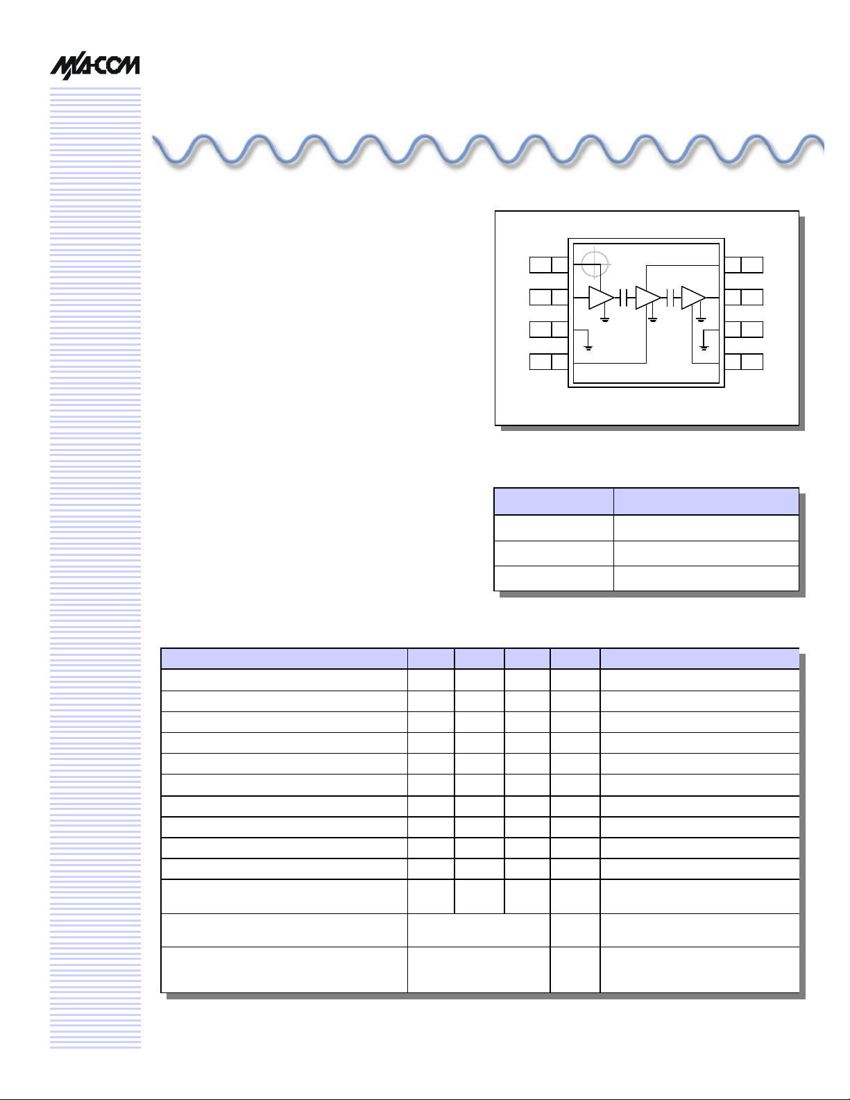
M/A-COM’s AM52-0024 is a 0.5 W, 2.4 GHz GaAs
MMIC, power amplifier in a low-cost MSOP-8 package. It
employs some external matching to obtain optimum input
return loss and output power performance. The AM520024 may be operated with supply voltages of +3.3 V to
+5.5 V.
The AM52-0024 may be used in a wide variety of applic ations including WLAN, WDECT, and Bluetooth.
The AM52-0024 is fabricated using M/A-COM’s SelfAligned MSAG MESFET process to realize high power
efficiency, single supply voltage, and small size. The process features full passivation for increased performance and
reliability.
Functional Schematic
PIN 1
PIN 8
Ordering Information
Part Number Package
AM52-0024TR 7 inch, 1000 Piece Reel
AM52-0024TR-3000 13 inch, 3000 Piece Reel
AM52-0024SMB Sample Test Board
Electrical Specifications
Characteristic Min Typ Max Unit Test Conditions
Frequency 2.4 2.5 GHz
Output Power 25.5 27.5 dBm F = 2450 MHz, PIN = -2 dBm
Power Added Efficiency 57 % F = 2450 MHz, PIN = -2 dBm
Current Under Drive 300 mA F = 2450 MHz, PIN = -2 dBm
Current Under Linear Operation 130 230 300 mA F = 2450 MHz, P
Small Signal Gain 29.0 dB F = 2450 MHz, P
Harmonics -40 dBc F = 2450 MHz, PIN = -2 dBm
Input VSWR 1.4:1 2.0:1 - F = 2450 MHz, PIN = -2 dBm
Off Isolation 40 dB F = 2450 MHz, VDD = 0 V
Thermal Resistance, junction to package bottom 25 °C/W F = 2450 MHz, PIN = -2 dBm
Third Order Intercept Point 40 dBm F1 = 2450 MHz, PIN = -20 dBm
Load Mismatch No Degradation in Power
Stability - PIN = -2 to +2 dBm, VDD = 0 to 5.5 V,
1. VDD = +3.3 Volts, PIN = -2 dBm, Frequency = 2450 MHz, and Duty Cycle = 100% unless otherwise specified.
2. All Measurements taken in a 50 Ω system unless otherwise specified.
1,2
: TS = +37°C (temperature measured at the soldering point of the downset paddle)
= +20 dBm
OUT
= +20 dBm
OUT
F2 = 2451 MHz, PIN = -20 dBm
Output
All non-harmonically re-
lated outputs more than 60
dB below desired signal
- VDD = 5.5 V, VSWR = 8:1, PIN = 0 dBm
Load VSWR = 6:1, all phases
Page 2
0.5 W, 2.4 GHz Power Amplifier
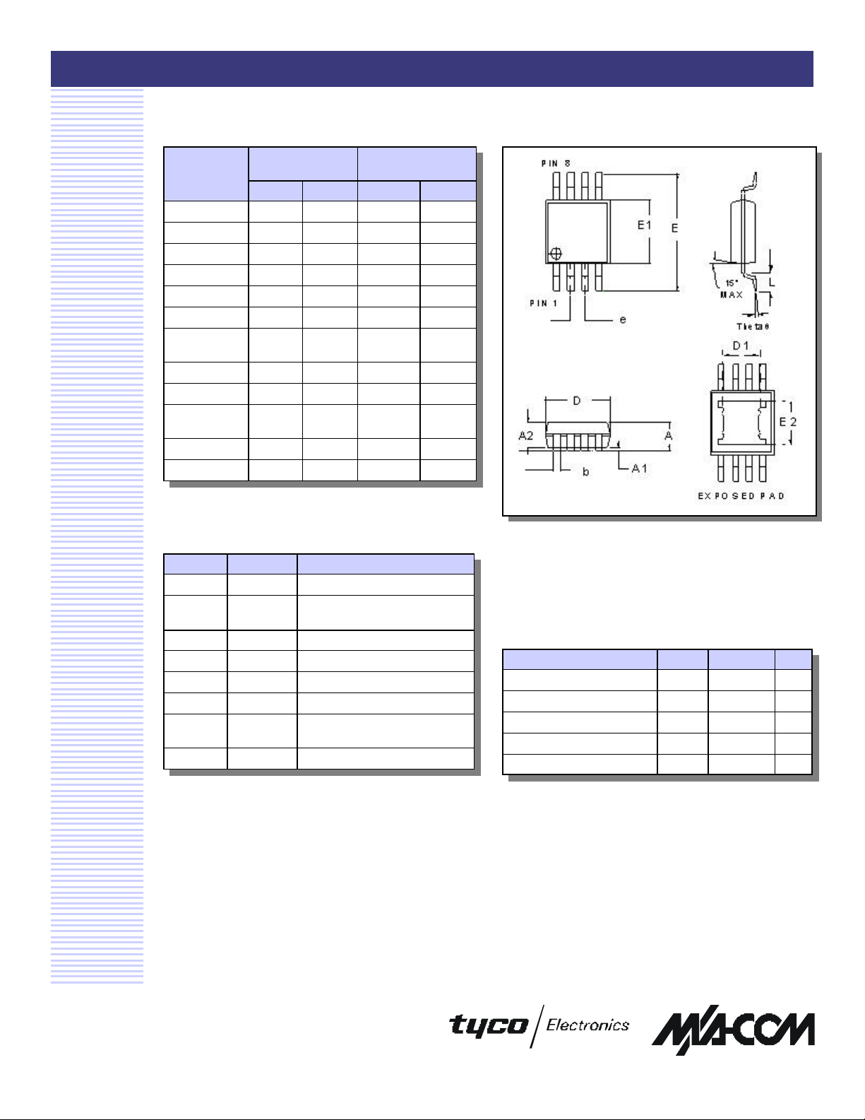
MSOP-8EP Plastic Package
AM52- 0024
V 1.4
Dimensions
A 0.80 1.10 0.0315 0.0433
A1 0.026 0.076 0.0010 0.0030
A2 0.75 0.95 0.0295 0.0374
b 0.25 0.40 0.0098 0.0157
D 2.90 3.10 0.1142 0.01220
D1 1.85 ref. 1.85 ref. 0.073 ref. 0.073 ref.
E 4.90
E1 2.90 3.10 0.1142 0.1220
E2 1.73 ref 1.73 ref. 0.068 ref. 0.068 ref.
e 0.65
L 0.40 1.70 0.0157 0.0276
Theta (θ) 0° 6° 0° 60°
Pin Configuration
Pin
1 VD1 Drain Voltage for First Stage
2 RFIN/VG1 RF input and Gate Voltage for
3 GND Ground
4 VG2 Gate Bias for Second Stage
5 VG3 Gate Bias for Third Stage
6 GND Ground
7 RF
8 VD2 Drain Voltage for Second Stage
Measurement
(mm)
Min Max Min Max
basic
basic
Function Description
OUT/VD3
4.90
basic
0.65
basic
3
RF Output and Drain Voltage for
Measurement
0.1929
basic
0.0256
basic
First Stage
Third Stage
(inches)
0.1929
0.0256
basic
basic
Note: All dimensions per JEDEC MO-187 Var. AA (issue B)
except for D1, E2, and A1. See JEDEC or contact M/A-COM for
additional dimensional and tolerance information.
Absolute Maximum Ratings
Rating
DC Supply Voltage VDD 5.5 V
RF Input Power PIN 10 mW
Junction Temperature TJ 150 °C
Storage Temperature Range T
Operating Temperature T
Symbol Value Unit
-40 to +150 °C
STG
-40 to +100 °C
OPER
4
3. Package bottom is electrical and thermal ground
Specifications subject to change without notice.
n North America: Tel. (800) 366-2266
n Asia/Pacific: Tel.+81-44-844 -8296, Fax +81-44-844-8298
n Europe: Tel. +44 (1344) 869 595, Fax+44 (1344) 300 020
Visit www.macom.com for additional data sheets and product information.
4. Exceeding these limits may cause permanent damage.
2
Page 3

0.5 W, 2.4 GHz Power Amplifier
Application Information
AM52- 0024
V 1.4
Specifications subject to change without notice.
n North America: Tel. (800) 366-2266
n Asia/Pacific: Tel.+81-44-844 -8296, Fax +81-44-844-8298
n Europe: Tel. +44 (1344) 869 595, Fax+44 (1344) 300 020
Visit www.macom.com for additional data sheets and product information.
3
Page 4

0.5 W, 2.4 GHz Power Amplifier
IN
DD
L2 1 2 3 4 5 6 7 8 T2
T1
L1
T5
C3
Downset Paddle
To Board Ground
T7
Evaluation Board Schematic
+V
RF
C1
List of components:
C1 – C4 = 100 pF multilayer ceramic chip capacitor (Dielectric Labs C11AH101K5TXL)
C5 = 2.0 pF multilayer c eramic chip capacitor (Dielectric Labs C11AH2R0B5TXL)
C6 = 1.2 pF multilayer ceramic chip capacitor (Dielectric Labs C11AH1R2B5TXL)
R1 = 300 Ω chip resistor (P300ECT -ND)
L1 = 1.8 nH chip inductor (Toko TKS2360CT -ND)
L2 = 27 nH chip inductor (Coilcraft 100 8CS-270XKBB)
R1
T4
T3
C2
Full-
C4
AM52- 0024
V 1.4
T8
RF
OUT
T6
C5
C6
Transmission Line
T1 0.15 inches 0.077 inches
T2 0.21 inches 0.077 inches
T3 0.11 inches 0.077 inches
T4 0.16 inches 0.026 inches
T5 0.13 inches 0.077 inches
T6 0.16 inches 0.077 inches
T7 0.13 inches 0.026 inches
T8 0.07 inches 0.026 inches
* Lengths and widths are given for a 0.060 inch thick FR-4 board
(distance between RF and ground planes) with dielectric constant
of approximately 4.3.
Length Width
Specifications subject to change without notice.
n North America: Tel. (800) 366-2266
n Asia/Pacific: Tel.+81-44-844 -8296, Fax +81-44-844-8298
n Europe: Tel. +44 (1344) 869 595, Fax+44 (1344) 300 020
Visit www.macom.com for additional data sheets and product information.
4
Page 5

0.5 W, 2.4 GHz Power Amplifier
Gain (dB)
Typical Performance Curves
Gain vs. Frequency, over Temperature
AM52- 0024
V 1.4
Input Return Loss vs. Frequency, over Temperature
30
29
28
27
26
25
2.2 2.3 2.4 2.5 2.6
Drain Current vs. Frequency, over Temperature Gain and Drain Current vs. Voltage, TS = +37 °C
-40C
+25C
+85C
Frequency (GHz)
35
30
25
20
Gain (dB)
15
1 2 3 4 5
Gain
Idd
450
350
250
150
50
Idd (mA)
Output Power and Drain Current vs. Input Power,
TS = +37 °C
Specifications subject to change without notice.
n North America: Tel. (800) 366-2266
n Asia/Pacific: Tel.+81-44-844 -8296, Fax +81-44-844-8298
n Europe: Tel. +44 (1344) 869 595, Fax+44 (1344) 300 020
Visit www.macom.com for additional data sheets and product information.
Vdd (volts)
5
Page 6

0.5 W, 2.4 GHz Power Amplifier
Designing With the AM52- 0024
The AM52-0024 is built using a near -enhancement mode FET that operates from a single supply voltage. A negative
voltage is not required because the FET is designed to operate with a +0V DC gate bias.
To duplicate AM52-0024 data sheet performance, the circuit board must present the same impedances realized on
this evaluation board. The table below has impedance measurements looking into the traces on the evaluation board,
AM52- 0024
V 1.4
Frequency V
GHz MAG ANG MAG ANG MAG ANG MAG ANG MAG ANG
0.2 0.98890 168.89 0.98437 158.43 0.98990 157.75 0.96758 88.92 0.98740 170.03
0.3 0.88449 130.14 0.97810 148.00 0.98811 147.07 0.93440 52.01 0.87259 126.11
0.4 0.96296 162.21 0.96932 138.02 0.98733 136.83 0.89791 28.02 0.95647 168.46
0.5 0.98166 159.36 0.96033 128.52 0.98729 126.92 0.85525 8.85 0.97951 165.71
0.6 0.98669 150.11 0.95221 119.37 0.98779 117.53 0.80306 -8.42 0.98325 157.06
0.7 0.98659 142.94 0.94257 110.68 0.98796 108.67 0.75165 -23.19 0.98331 150.64
0.8 0.98701 136.46 0.93372 102.50 0.98912 100.34 0.70235 -36.51 0.98362 144.92
0.9 0.98696 130.40 0.92399 94.78 0.98928 92.48 0.65785 -49.03 0.98291 139.57
1.0 0.98757 124.64 0.91521 87.48 0.99004 85.10 0.61674 -61.22 0.98248 134.49
1.1 0.98793 119.13 0.90655 80.60 0.99099 78.16 0.58189 -73.60 0.98325 129.55
1.2 0.98766 113.79 0.89741 74.13 0.99165 71.67 0.55207 -86.36 0.98254 124.75
1.3 0.98685 108.52 0.88850 68.01 0.99162 65.55 0.52778 -99.76 0.98097 119.95
1.4 0.98253 103.08 0.87922 62.20 0.99228 59.78 0.51054 -113.87 0.97567 14.77
1.5 0.91016 98.26 0.87041 56.61 0.99283 54.27 0.50134 -128.62 0.88506 109.11
1.6 0.97895 96.95 0.85901 51.24 0.99372 49.02 0.50184 -143.72 0.96660 110.93
1.7 0.98693 91.94 0.84867 46.25 0.99362 44.08 0.51099 -159.03 0.97912 105.76
1.8 0.98885 87.51 0.83780 41.39 0.99411 39.33 0.52890 -174.06 0.98174 101.51
1.9 0.98968 83.39 0.82602 36.67 0.99457 34.73 0.55378 171.57 0.98247 97.56
2.0 0.99001 79.46 0.81268 32.09 0.99405 30.31 0.58373 158.06 0.98252 93.75
2.1 0.98939 75.68 0.79856 27.65 0.99409 26.02 0.61689 145.85 0.96646 89.86
2.2 0.9079 72.12 0.78264 23.35 0.99430 21.85 0.65283 133.76 0.98349 87.18
2.3 0.99100 68.61 0.76563 19.11 0.99427 17.75 0.68573 123.12 098395 83.71
2.4 0.99134 65.25 0.74652 14.96 0.99425 13.76 0.71788 113.31 0.98474 80.41
2.5 0.99146 61.98 0.72506 10.91 0.99399 9.82 0.74798 104.32 0.98447 77.23
2.6 0.99178 58.73 0.70186 6.91 0.99400 5.85 0.77528 95.95 0.98507 74.04
2.7 0.99134 55.49 0.67587 2.97 0.99331 1.90 0.79976 88.27 0.98381 70.83
2.8 0.98781 52.20 0.64683 -0.91 0.99282 -2.00 0.82079 81.13 0.98006 67.52
2.9 0.96980 48.90 0.61470 -4.81 0.99214 -5.98 0.83832 74.49 0.96403 63.91
3.0 0.95172 48.55 0.57400 -8.86 0.99108 -9.98 0.85400 68.30 0.90400 62.55
3.1 0.98242 46.16 0.52740 -11.19 0.98954 -13.99 0.86663 62.57 0.95087 63.65
3.2 0.99063 43.08 0.48956 -13.34 0.98827 -18.12 0.87801 57.07 0.97696 60.24
3.3 0.99392 40.27 0.44620 -15.29 0.98684 -22.42 0.88698 51.92 0.98397 57.19
3.4 0.99353 37.51 0.40182 -16.23 0.98579 -26.81 0.89353 46.93 0.98539 54.35
3.5 0.99183 34.87 0.35797 -15.65 0.98338 -31.29 0.89823 42.18 0.98374 51.69
3.6 0.98528 32.36 0.31683 -13.12 0.98114 -36.02 0.90042 37.52 0.97595 49.24
3.7 0.98115 30.74 0.28368 -7.89 0.97774 -40.95 0.89832 32.95 0.97468 47.68
3.8 0.99055 28.59 0.26456 -0.17 0.97527 -46.15 0.88711 28.34 0.98255 45.41
3.9 0.99468 26.15 0.26206 8.43 0.97149 -51.66 0.85217 23.98 0.98187 42.91
4.0 0.99541 23.85 0.27526 16.18 0.96801 -57.48 0.78439 25.69 0.97076 41.20
Pin 1 RFIN/V
DD1
Pin 2 V
GG1
Specifications subject to change without notice.
n North America: Tel. (800) 366-2266
n Asia/Pacific: Tel.+81-44-844 -8296, Fax +81-44-844-8298
n Europe: Tel. +44 (1344) 869 595, Fax+44 (1344) 300 020
Visit www.macom.com for additional data sheets and product information.
Pin 4 RF
GG2
OUT/VDD3
Pin 7 V
DD2
Pin 8
6
 Loading...