

Page 1
GaAs MMIC VSAT Power Amplifier 2.0W
14.0 - 14.5 GHz
AM42-0007
Features
• High Linear Gain: 22 dB Typ.
• High Saturated Output Power: +33 dBm Typ.
• High Power Added Efficiency: 22% Typ.
• High P
: 32 dBm Typ.
1dB
• 50Ω=Input/Output Broadband Matched
• Integrated Output Power Detector
• High Performance Ceramic Bolt Down Package
Description
M/A-COM’s AM42-0007 is a three-stage MMIC linear power
amplifier in a ceramic bolt down style hermetic package. The
AM42-0007 employs a fully matched chip with internally
decoupled Gate and Drain bias networks and an ouput power
detector. The AM42-0007 is designed to be operated from a
constant voltage Drain supply.
The AM42-0007 is designed for use as an output stage or a
driver, in applications for VSAT systems. This design is fully
monolithic and requires a minimum of external components.
M/A-COM’s AM42-0007 is fabricated using a mature 0.5
micron GaAs MESFET process. The process features full
passivation for increased performance and reliability. This
product is 100% RF tested to ensure compliance to performance
specifications.
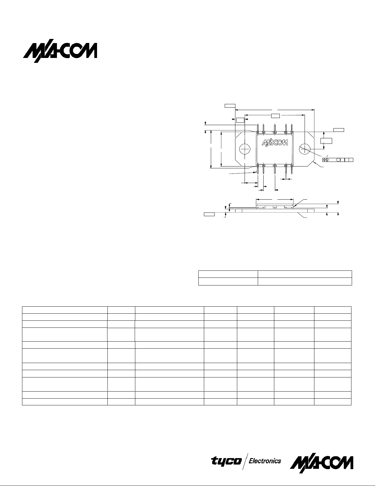
CR-15
.050 MIN. 10
X
.328 ± .010
.318 ± .010
.010 SQ .
ORIENTATION TAB
- A -
.115 ± .010
.030
- C -
.085
.050 4X
.005 ± .002
Notes: (unless otherwise specified)
1. Dimensions are in inches.
2. Tolerance: .XXX = ± 0.005
.XX = ± 0.010
.70
.530
8 9 10
6
7
.159
2X o .096 THRU
2 1
.33
5 4 3
.010 ± .003 10
X
.100 4X
CERAMIC
BASE PLATE
Ordering Information
Part Number Package
AM42-0007 Ceramic Bolt Down Package
- B -
o.004 M A B C
4X .06 X 45°
CHAMFER
.090 MAX
.040
Electrical Specifications: T
= +25°C, VDD = +9V, VGG = -5.0V, Z0 = 50Ω,
C
Parameter Abbv. Test Conditions Units Min. Typ. Max.
Linear Gain G
Input VSWR
Output VSWR
Saturated Output Power P
Output Power @
Output IP3
Power Added Efficiency
Bias Currents I
Thermal Resistance
Detector Output Voltage V
is measured with two +24 dBm output tones @ 1 MHz spacing.
IP
3
Specifications subject to change without notice.
North America: Tel. (800) 366-2266, Fax (800) 618-8883
Asia/Pacific: Tel.+81-44-844-8296, Fax +81-44-844-8298
Europe: Tel. +44 (1344) 869 595, Fax+ 44 (1 34 4) 30 0 020
Visit www.macom . com for ad di tional data sheets and pr o d uct i nf orm ation.
VSWR
VSWR
T
SAT
P
1dB
IP
PAE
GG
θ
JC
det
L
IN
OU
3
P
≤ 0 dBm
IN
P
≤ 0 dBm
IN
P
≤ 0 dBm
IN
P
= +14 dBm
IN
— dBm 31 32 —
(Refer to Note 1) dBm — 41 —
= +14 dBm
P
IN
P
= +14 dBm
IN
25°C Heat Sink °C/W — 9.5 —
RL=10KΩ, P
OUT
=+31dBm
Ω,====Frequency = 14.0-14.5 GHz
Ω,Ω,
dB 19 22 —
— — 2.5:1 2.7:1
— — 2.7:1 —
dBm — 33 —
% — 22 —
mA 18 25
V — +3.5 —
V 4.0
1
Page 2
GaAs MMIC VSAT Power Amplifier 2.0W, 14.0 - 14.5 GHz
AM42-0007
Absolute Maximum Ratings
1,2,3,4
Parameter Absolute Maximum
V
DD
V
GG
12 Volts
-10 Volts
Power Dissipation 13.2 W
RF Input Power +23 dBm
Channel Temperature 150°C
Storage Temperature -65°C to +150°C
I
ds
1. Operation of this device outside any of these limits may cause
permanent damage.
2. Case Temperature (T
3. Nominal bias is obtained by first connecting -5 volts to pin 4 (V
followed by connection +9 volts to pin 6 (V
4. RF ground and thermal interface is the flange (case bottom).
Adequate heat sinking is required.
5. No dc bias voltage appears at the RF ports.
6. The dc resistance at the input port is an open circuit and at the
ouput port is a short circuit.
7. For optimum IP
be placed within 0.5 inches of pin 6.
) = +25°C.
C
performance, the V
3
DD
2100 mA
). Note sequence.
DD
bypass capacitors should
V
DD
3,4,7
3.3
µ F
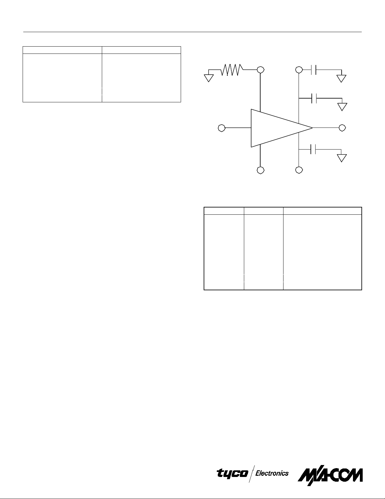
Typical Bias Configuration
10 K
Ω
V
det
7 6
µ
F
0.01
),
GG
3
IN OUT
AM42-0007
GND
1,2,5,9,10 4
0.01
V
GG
µ F
8
Pin Configuration
Pin No. Pin Name Description
1 GND DC and RF Ground
2 GND DC and RF Ground
3 IN RF Input
4 V
GG
5 GND DC and RF Ground
6 V
7 V
DD
det
8 OUT RF Output
9 GND
10 GND DC and RF Ground
Gate Supply
Voltage Drain Supply
Output Power Detector
DC and RF Ground
Specifications subject to change without notice.
North America: Tel. (800) 366-2266, Fax (800) 618-8883
Asia/Pacific: Tel.+81-44-844-8296, Fax +81-44-844-8298
Europe: Tel. +44 (1344) 869 595, Fax+ 44 (1 34 4) 30 0 020
Visit www.macom . com for ad di tional data sheets and pr o d uct i nf orm ation.
V 4.0
2
Page 3

GaAs MMIC VSAT Power Amplifier 2.0W, 14.0 - 14.5 GHz
Typical Performance @ +25°C
Test Conditions are listed in the section “Electrical Specifications”.
AM42-0007
Linear Gain vs. Frequency Input and Output Return Loss vs. Frequency
25
15
5
25
15
5
S11 S22
-5
Linear Gain (dB)
-15
10 12 14 16 18
Frequency (GHz)
Output Power vs. Input Power
@ 14.25 GHz
35
P
33
31
(dBm)
29
OUT
P
27
25
0
4 8 12 16
PIN (dBm)
OUT
PAE
50
40
30
20
10
0
-5
Magnitude (dB)
-15
10 12
14
Frequency (GHz)
Detector Voltage vs. Output Power
@ 14.25 GHz
6
5
4
3
(V)
2
DET
V
1
0
19 21 23 25 27 29 31 33
P
OUT
(dBm)
16
18
Output Power vs. Frequency
= +14 dBm
@ P
IN
35
33
31
(dBm)
29
OUT
P
27
25
12
13
Frequency (GHz)
14 15 16
Power Added Efficiency vs. Frequency
@ PIN = +14 dBm
50
40
30
20
PAE (%)
10
0
12
13
14
Frequency (GHz)
15
16
Specifications subject to change without notice.
North America: Tel. (800) 366-2266, Fax (800) 618-8883
Asia/Pacific: Tel.+81-44-844-8296, Fax +81-44-844-8298
Europe: Tel. +44 (1344) 869 595, Fax+ 44 (1 34 4) 30 0 020
Visit www.macom . com for ad di tional data sheets and pr o d uct i nf orm ation.
V 4.0
3
 Loading...