

Datasheet Am29SL800CT150WBIB, Am29SL800CT150WBI, Am29SL800CT150WBCB, Am29SL800CT150WBC, Am29SL800CT150FIB Datasheet (AMD Advanced Micro Devices)
...Page 1

PRELIMINARY
Am29SL800C
8 Megabi t (1 M x 8-Bit/51 2 K x 16-Bit)
CMOS 1.8 Volt-only Super Low Volta ge Flash Memory
DISTINCTIVE CHARACTERISTICS
■ Single p ower supply operation
— 1.8 to 2.2 V for read, program, and erase
operations
— Ideal for battery-powered applications
■ Manufactured on 0.32 µm process technology
— Compatible with 0.35 µm Am29SL800B device
■ High performance
— Access times as fast as 100 ns
■ Ultra low power consumption (typical values at
5 MHz)
— 65 nA Automatic Sleep Mode current
— 65 nA standby mode current
— 5 mA read current
— 10 mA program/erase current
■ Flexible sector architecture
— One 16 Kbyte, two 8 Kbyte, one 32 Kbyte, and
fifteen 64 Kbyte sectors (byte mode)
— One 8 Kword, two 4 Kword, one 16 Kword, and
fifteen 32 Kword sectors (word mode)
— Supports full chip erase
— Sector Protection features:
A hardwar e me tho d of lockin g a sec to r to
prevent any program or erase operations wi thin
that sector
Sectors can be locked in-system or via
programming equipment
T emporary Sector Unprotect feature allows code
changes in previously locked sectors
■ Unlock Bypass Program Command
— Reduces overall programming time when
issui ng mult iple program command sequences
■ Top or bottom boot block configurations
available
■ Embedded Algorithms
— Embedded Erase algorithm automatically
preprograms and erases the entire chip or any
combination of designated sectors
— Embedded Program algorithm automatically
writes and verifies data at specified addresses
■ Minimum 1,000,000 write cycle guarantee per
sector
■ Package option
— 48-pin TSOP
— 48-ball FBGA
■ Compatibility with JEDEC standards
— Pinout and software compatible with single-
power supply Flash
— Superior inadvertent write protection
■ Data# Polling a nd toggle bits
— Provides a software method of detecting
program or erase operation completion
■ Ready/Bu sy # pin (RY/BY#)
— Provides a hardware method of detecting
program or erase cycle completion
■ Erase Sus pe nd /Er as e R es ume
— Suspends an erase operation to read data from,
or program data to, a sector th at is not being
erased, then resumes the erase operation
■ Hardware reset pin (RESET#)
— Hardware method to reset the device to reading
array data
This do c um ent contains information on a product under d evel opment at A dvanced Mi c r o Devices. The inform ation
is intended to help you evaluate this product. AMD reserves the right to change or discontinue work on this proposed
product without notice.
Refer to AMD’s Website (www.amd.com) for the latest information.
Publication# 22230 Rev: A Amendment/0
Issu e Dat e: August 1998
Page 2

PRELIMINARY
GENERAL DESCRIPTION
The Am 29SL 800C i s an 8 M bit, 1.8 V vol t-only Flas h
memory organized as 1,048,576 bytes or 524,288
words. The d evice is offe red in 48 -pin TSOP and 48 ball FBGA packages. The word-wide data (x16)
appears on DQ15–DQ0; the byte-wide (x8) data
appear s on DQ7– DQ0. T his de vice is d esigne d to be
programmed and erased in-system with a single 1.8
volt V
The device c an also be program med in standard
EPROM programmers.
The standard device offers access times of 100, 120,
and 150 ns, allowing high speed microprocessors to
operate without wait states. To eliminate bus contention
the device has separate chip enable (CE#), write
enable (WE#) and output enable (OE#) controls.
The de vi ce re q ui r es on l y a single 1.8 volt power sup-
ply for both read and write functions. Internally generated and regulated voltage s are provided for th e
program and erase operations.
The device is entirely command set compatible with the
JEDEC single-power-supply Flash standard. Commands are written to the command register using
standard microprocessor write timings. Register contents serve as input to an internal state-machine that
controls the erase and programming circuitr y. Write
cycles also internally latch addresses and data needed
for the programming and erase operations. Reading
data ou t of the d evice is simi lar to re ading fr om othe r
Flash or EPRO M devices .
Device pro gram m ing oc cu rs by executing the program
command sequence. This initiates the Embedded
Program algorithm—an internal algorithm that automatically times the program pulse widths and verifies
proper cell margin. The Unlock Bypass mode facilitates faster programming times by requiring only two
write cycles to program data instead of four.
Device erasure occurs by ex ecuting the erase command
sequence. This initiates the Embedded Erase algorithm—an i nternal algo rithm tha t automatically prep rograms the array (if it is not already programmed) before
executing the erase operation. During erase, the device
automatically times the erase pulse widths and verifies
proper cell margin.
supply. No VPP is for wr ite or era se oper ations .
CC
The ho st system ca n detect whe ther a progra m or
erase op eration is co mp lete by ob ser vin g t he RY/BY#
pin, or by reading the DQ7 (Data# Polling) and DQ6
(toggle ) st atus bit s. After a program or erase cycle has
been completed, the device is ready to read array data
or accept another command.
The sector erase architecture allows memory sectors
to be erased and reprogrammed without affecting the
data contents of other sectors. The device is fully
eras ed when shipped f r om the factory.
Hardware data protection measures includ e a low
V
detector that auto matically inhibits write opera-
CC
tions during power transitions. The hardware sector
protection feature disables both program and erase
operatio ns in any com binatio n of the s ectors of m emory. This can be achieved in-system or via programming equipment.
The Erase Suspend feature enables the user to put
erase on ho ld for any pe r i od of tim e to rea d da ta fr om ,
or program d ata to, any secto r that is not se lected for
erasure. True background erase can thus be achieved.
The hardware RESET# pin terminates any operation
in progress and resets the internal state machine to
reading array data. T he RESET# pin ma y b e tied to t he
system rese t circuitr y. A system reset would thus a lso
reset the device, enabling the system micropr ocessor
to read the boot-up firmware from the Flash memory.
The device offers two power-saving features. When addresses have been stable for a specified amount of
time, the device enters the automatic sleep mode.
The system can also place the device into the standby
mode. Power consumption is greatly reduced in both
these modes.
AMD’s Flash technology combines years of Flash
memory manufacturing experience to produce the
highest levels of quality, reliability and cost effectiveness. The device electrically erases all bit s with in
a sector simultaneously via Fowler-Nordheim tunneling. The data is programmed using hot electron
injection.
2 Am29SL800C
Page 3
PRELIMINARY
PRODUCT SELECTOR GUIDE
Family Part Number Am29SL800C
Speed Options 100 120 150
Max access time, ns (t
Max CE# access time, ns (tCE) 100 120 150
Max OE# access time, ns (tOE) 35 50 65
) 100 120 150
ACC
Note: See “AC Characteristics” for full specifications.
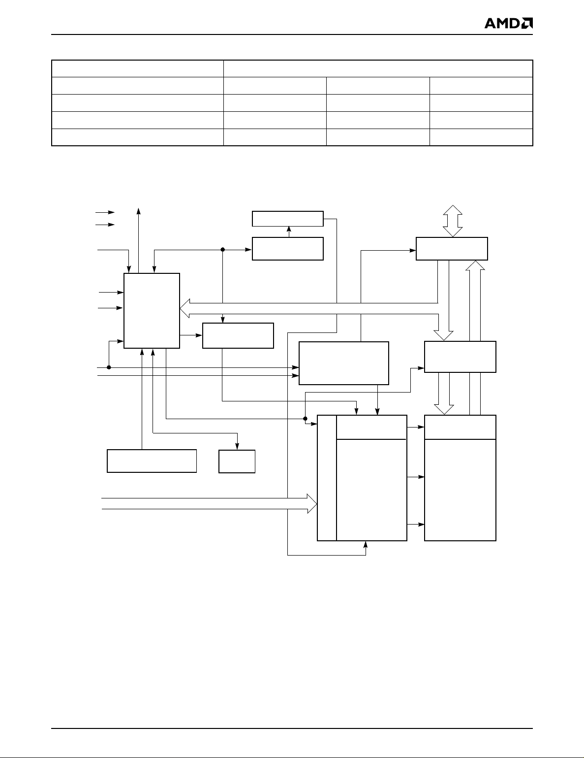
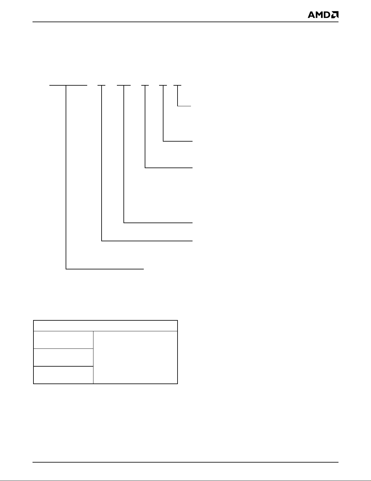
BLOCK DIAGRAM
DQ0
–
DQ15 (A-1)
Input/Output
Buffers
Data
Latch
V
CC
V
SS
RESET#
WE#
BYTE#
CE#
OE#
RY/BY#
State
Control
Command
Register
PGM Voltage
Generator
Sector Switches
Erase Voltage
Generator
Chip Enable
Output Enable
Logic
STB
A0–A18
VCC Detector
Timer
STB
Address Latch
Y-Decoder
X-Decoder
Y-Gating
Cell Matrix
22230A-1
Am29SL800C 3
Page 4
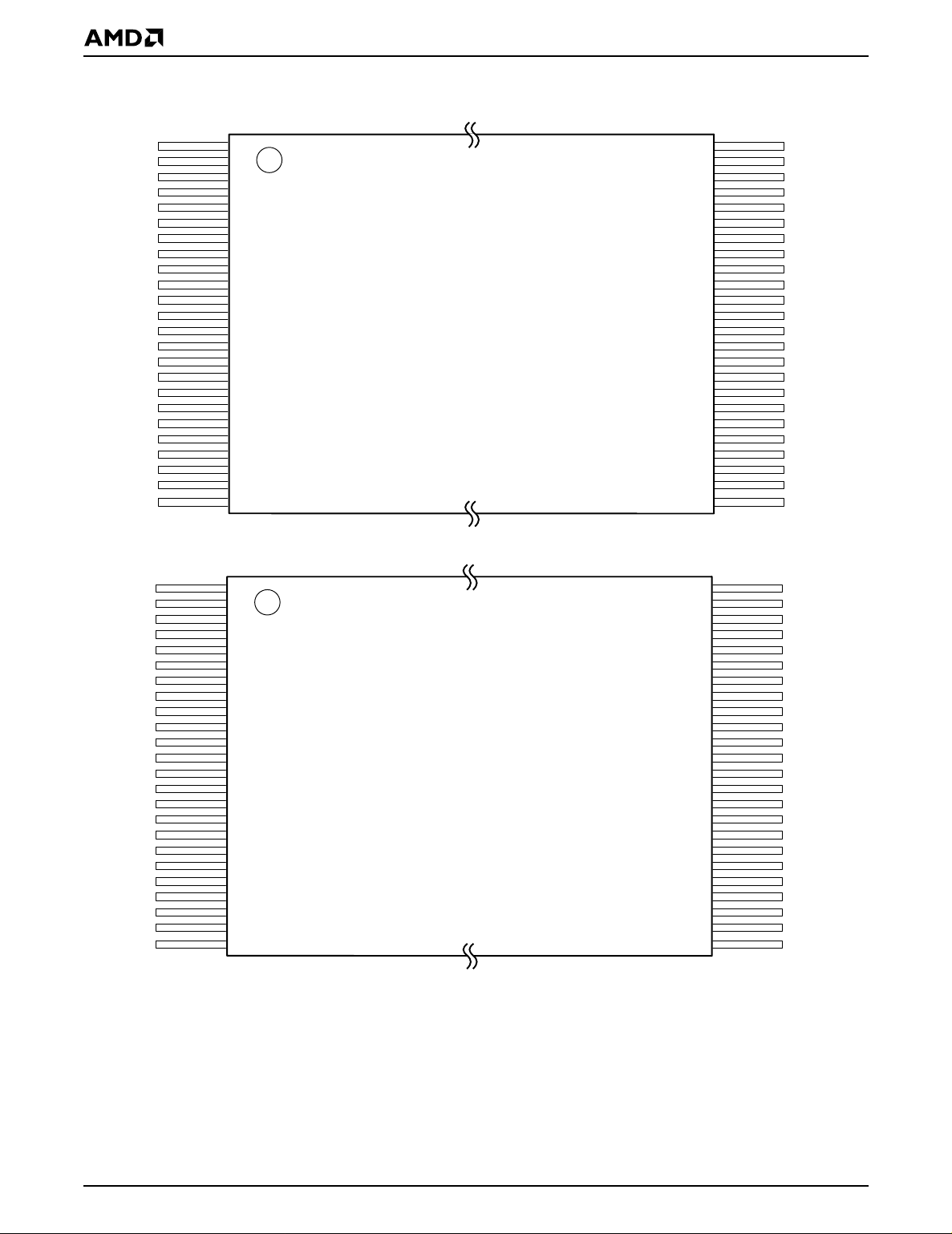
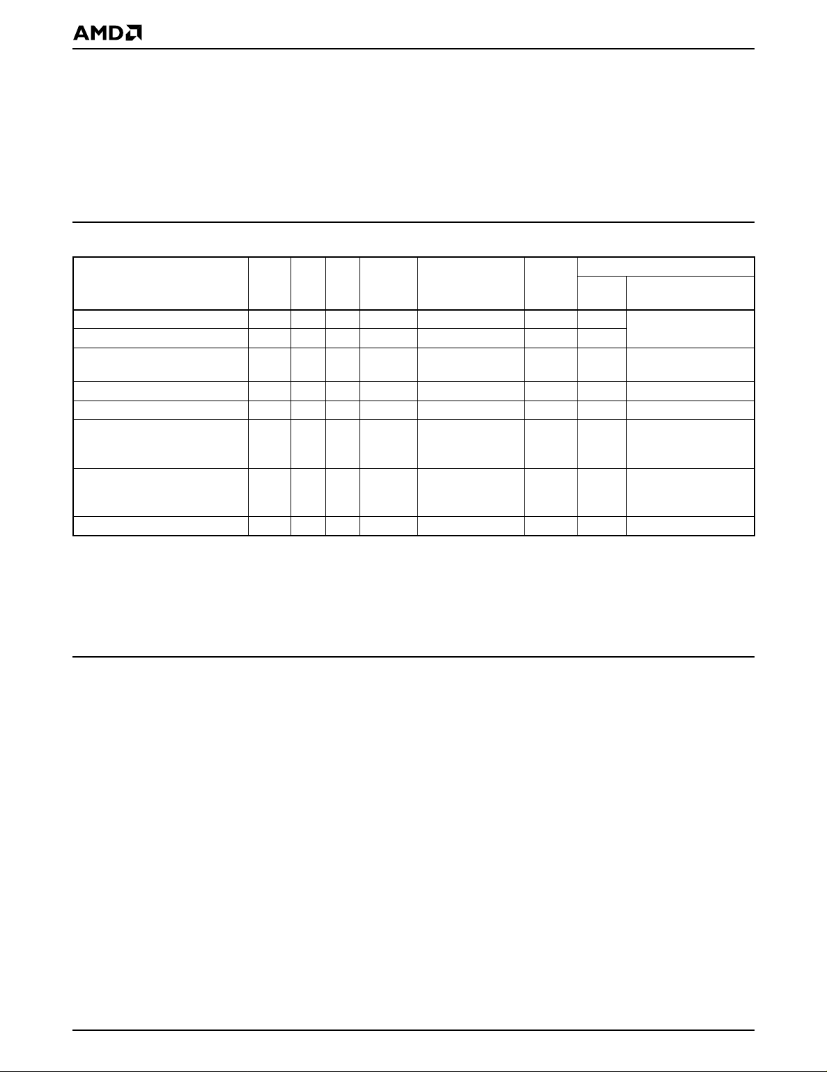
CONNECTION DIAGRAMS
PRELIMINARY
A15
A14
A13
A12
A11
A10
A9
A8
NC
NC
WE#
RESET#
NC
NC
RY/BY#
A18
A17
A7
A6
A5
A4
A3
A2
A1
A16
BYTE#
V
SS
DQ15/A-1
DQ7
DQ14
DQ6
DQ13
DQ5
DQ12
DQ4
V
CC
DQ11
DQ3
DQ10
DQ2
DQ9
DQ1
DQ8
DQ0
OE#
V
SS
CE#
A0
1
2
3
4
5
6
7
8
9
10
11
12
13
14
15
16
17
18
19
20
21
22
23
24
1
2
3
4
5
6
7
8
9
10
11
12
13
14
15
16
17
18
19
20
21
22
23
24
Standard TSOP
Reverse TSOP
48
47
46
45
44
43
42
41
40
39
38
37
36
35
34
33
32
31
30
29
28
27
26
25
48
47
46
45
44
43
42
41
40
39
38
37
36
35
34
33
32
31
30
29
28
27
26
25
A16
BYTE#
V
SS
DQ15/A-1
DQ7
DQ14
DQ6
DQ13
DQ5
DQ12
DQ4
V
CC
DQ11
DQ3
DQ10
DQ2
DQ9
DQ1
DQ8
DQ0
OE#
V
SS
CE#
A0
A15
A14
A13
A12
A11
A10
A9
A8
NC
NC
WE#
RESET#
NC
NC
RY/BY#
A18
A17
A7
A6
A5
A4
A3
A2
A1
4 Am29SL800C
22230A-2
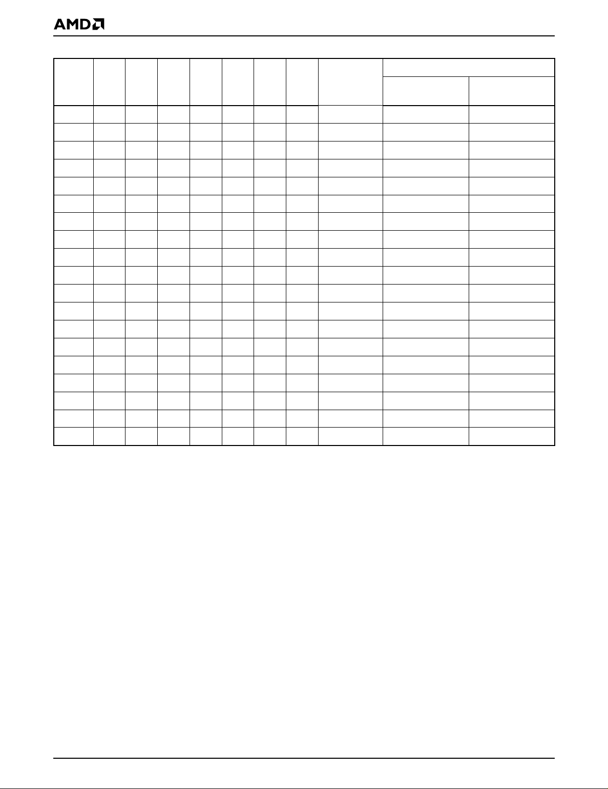
Page 5
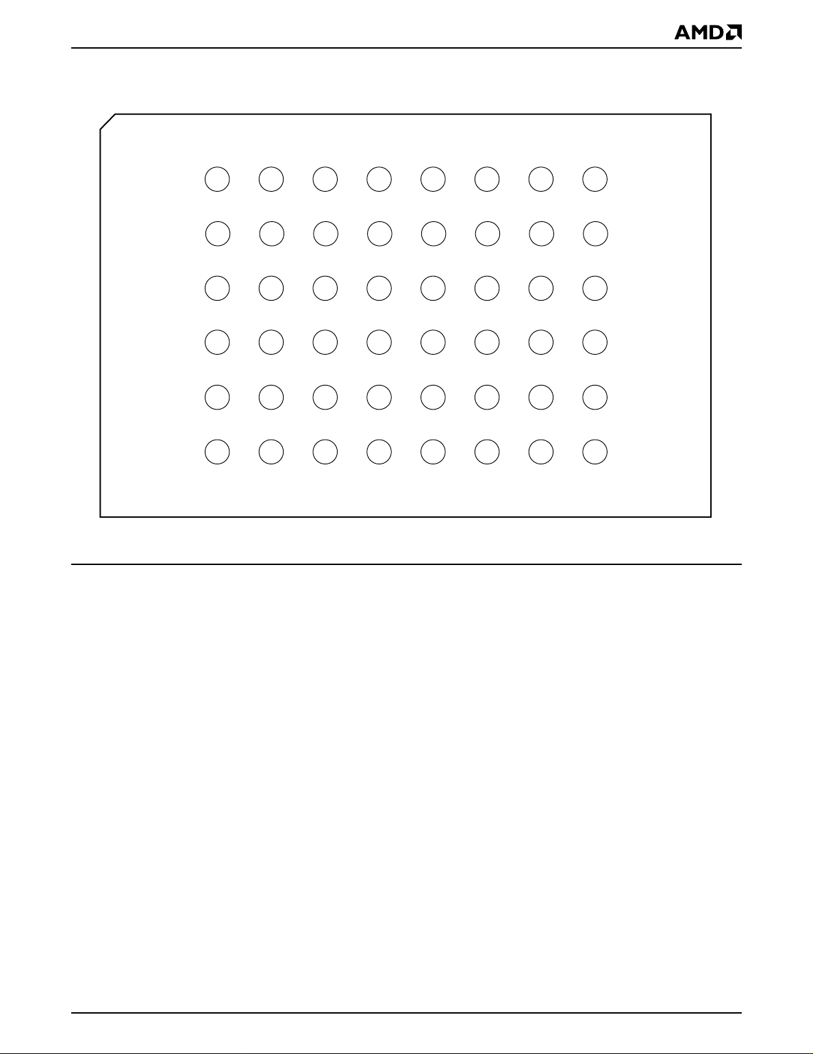
CONNECTION DIAGRAMS
A1 B1 C1 D1 E1 F1 G1 H1
PRELIMINARY
48-Ball FBGA (Bottom View)
A2 B2 C2 D2 E2 F2 G2 H2
A3 B3 C3 D3 E3 F3 G3 H3
A4 B4 C4 D4 E4 F4 G4 H4
A5 B5 C5 D5 E5 F5 G5 H5
A6 B6 C6 D6 E6 F6 G6 H6
Special Handling Instructions for FBGA Packages
Special handling is required for Flash Memory products
in FBGA packages.
CE#A0A1A2A4A3
BYTE#A16A15A14A12A13
OE# V
DQ9 DQ1DQ8DQ0A5A6A17A7
DQ11 DQ3DQ10DQ2NCA18NCRY/BY#
V
CC
DQ13 DQ6DQ14DQ7A11A10A8A9
DQ15/A-1 V
SS
DQ4DQ12DQ5NCNCRESET#WE#
SS
22230A-3
Flash memory devices in FBGA packages may be
damaged if exposed to ultrasonic cleaning methods.
The package and/or data integrity may be compromised
if the package body is exposed to temperatures above
150°C for prolonged periods of time.
Am29SL800C 5
Page 6
PRELIMINARY
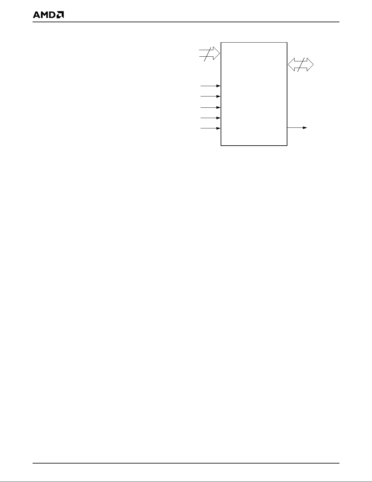
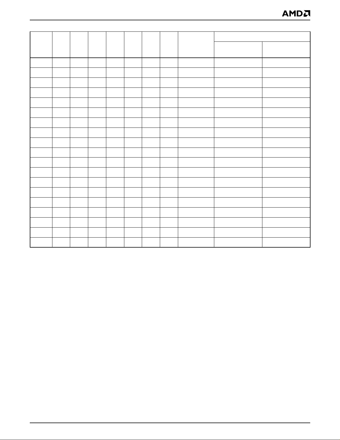
PIN CONFIGURATION
A0–A18 = 19 addresse s
DQ0–DQ14 = 15 data inputs/out pu ts
DQ15/A-1 = DQ15 (data input/output, word mode),
A-1 (LSB addre s s input, byte mode)
BYTE# = Selects 8-bit o r 16-bit mode
CE# = Chip enable
OE# = Output enable
WE# = Write en able
RESET# = Hardware reset pin, active low
RY/BY# = Ready/Busy# output
V
= 1.8–2.2 V single power supply
CC
V
SS
NC = Pin not connected internally
= Device ground
LOGIC SYMBOL
19
A0–A18
CE#
OE#
WE#
RESET#
BYTE# RY/BY#
16 or 8
DQ0–DQ15
(A-1)
22230A-4
6 Am29SL800C
Page 7
PRELIMINARY
ORDERING INFORMATION
Standard Products
AMD stan dard produc ts ar e available in several pack ages an d opera ting ranges. Th e orde r numbe r (Valid Comb ination) is formed by a combination of the elements below.
CE100Am29SL800C T
OPTIONAL PROCESSING
Blank = Standard Processing
B = Burn-in
(Contact an AMD representative for more information)
TEMPERATURE RANGE
C=Commercial (0°C to +70°C)
I = Industrial (–40°C to +85°C)
PACKAGE TYPE
E = 48-Pin Thin Small Outline Package (TSOP)
Standard Pinout (TS 048)
F = 48-Pin Thin Small Outline Package (TSOP)
Reverse Pinout (TSR048)
WB = 48-ball Fine-Pitch Ball Grid Array (FBGA)
0.80 mm pitch, 6 x 9 mm package
Am29SL800CT100,
Am29SL800CB100
Am29SL800CT120,
Am29SL800CB120
Am29SL800CT150,
Am29SL800CB150
Valid Combinations
EC, EI, FC, FI, WBC, WBI
SPEED OPTION
See Product Selector Guide and Valid Combinations
BOOT CODE SECTOR ARCHITECTURE
T = Top Sector
B = Bottom Sector
DEVICE NUMBER/DE SCRIP TION
Am29SL800C
8 Megabit (1 M x 8-Bit/512 K x 16-Bit) CMOS Flash Memory
1.8 Volt-only Read, Program, and Erase
Valid Combinations
Valid Combinations list configurations planned to be supported in volume for this device. Consult the local AMD sales
office to confirm availability of specific valid combinations and
to check on newly released combinations.
Am29SL800C 7
Page 8
PRELIMINARY
DEVICE BUS OPERATIONS
This section describes the requirements and use of the
device bus operat ions, whi ch are init iated thro ugh the
internal command register. The command register itself does not occupy any addressable memory location. The register is composed of latches that store the
comman ds, along with the add ress an d data infor mation needed to execute the command. The contents of
Table 1. Am29SL800C Device Bus Operations
Operation CE# OE# WE# RESET#
Read L L H H A
Write L H L H A
V
±
Standby
Output Disable L H H H X High-Z High-Z High-Z
Reset X X X L X High-Z High-Z High-Z
Sector Protect (Note 2) L H L V
Sector Unprotect (Note 2) L H L V
Temporary Sector Unprotect X X X V
Legend:
L = Logic Low = V
Notes:
1. Addresses are A18:A0 in word mode (BYTE# = V
2. The sector protect and sector unprotect functions may also be implemented via programming equipment. See the “Sector
Protection/Unprotection” section.
, H = Logic High = VIH, VID = 10 ± 1.0 V, X = Don’t Care, AIN = Address In, DIN = Data In, D
IL
CC
0.3 V
XX
VCC ±
0.3 V
ID
ID
ID
), A18:A-1 in byte mode (BYTE# = VIL).
IH
the register serve as inputs to the internal state machine. The state machine outputs dictate the function of
the device. Table 1 lists th e d evice bus o pe ratio ns, th e
inputs and control lev els they require, and the resulting
output. The following s ubsections describe each of
these operations in further detail.
DQ8–DQ15
Addresses
(Note 1)
IN
IN
X High-Z High-Z High-Z
Sector Address,
A6 = L, A1 = H,
A0 = L
Sector Address,
A6 = H, A1 = H,
A0 = L
A
IN
DQ0–
DQ7
D
OUT
D
IN
D
IN
D
IN
D
IN
BYTE#
= V
IH
D
OUT
D
IN
XX
XX
D
IN
BYTE#
= V
IL
DQ8–DQ14 = High-Z,
DQ15 = A-1
High-Z
= Data Out
OUT
W ord/Byte Configuration
The BY TE# p in contr ol s whethe r the device data I/O pins
DQ15–DQ0 operate in the byte or word configuration. If the
BYTE# pin is set at logic ‘1’, the device is in word configuration, DQ 15–DQ0 are ac tive and con trolled by CE # and
OE#.
If the BYTE# pin is set at logic ‘0’, the device is in byte configuration, and only data I/O pins DQ0–DQ7 are active and
controlled by CE# and OE#. The data I/O pins DQ8–DQ14
are tri-stated, and the DQ15 pin is used as an input for the
LSB (A-1) address function.
Requirements for Reading Array Data
The internal state machine is set for reading array data
upon device power-up, or after a hardware reset. This ensures that no spurious alteration of the memory content occurs during the power transition. No co mmand is
necessary in this mode to obtain array data. Standard microproce ssor read cy cles tha t asse rt valid ad dresse s on
the device address inputs produce valid data on the device
data outputs. The device remains enabled for read access
until the command register contents are altered.
See “Reading Array Data” for m ore informati on. Refer to
the AC Read Operations table for timing specifications and
to Figure 13 for the timing diagram. I
teristics table represents the active current specification for
reading array data.
To read array data from the outputs, the system must driv e
the CE# and OE# pins to V
selects the device. OE# is the output control and gates
array data to the ou tput pins. W E# shoul d rem ain at V
The BYTE# pin determines whether the device outputs
array data in words or bytes.
. CE# is the power control and
IL
Writing Commands/Command Sequences
To write a command or command seque nce (whic h in-
.
IH
cludes programming data to the device and erasing sectors
of memory), the syste m must drive WE# and CE# to V
and OE# to V
8 Am29SL800C
in the DC Charac-
CC1
,
.
IH
IL
Page 9

PRELIMINARY
For program operatio ns, the BYTE# pin deter mines
whether the dev ice accepts program data in bytes or
words. Refer to “Word/Byte Configuration” for more information.
The device features an Unlock Bypass mode to facilitate
faster programming. Once the device enters the Unlock
Bypass mode, only two write cycles are required to program a word or byte, instead of four. The “Word/Byte Program Command Sequence” section has details on
programming data to the device using bo th stand ard and
Unlock Bypass command sequences.
An erase operation can erase one sector, multiple sectors,
or the enti re device. Tables 2 and 3 indica te the add ress
space that eac h sector oc cup ie s. A “s ector addr ess ” co nsists of the address bits required to uniquely select a sector.
The “Command Definitions” section has details on erasing
a sector or the entire chip, or suspending/resuming the
erase operation.
After the system writes the autoselect command sequence, the device enters the autoselect mode. The system can then read autoselect codes from the internal
register (whic h is separate from the me mory array) on
DQ7–DQ0. Standard read cycle timings apply in this mode.
Refer to the Autoselect Mode and Autoselect Command
Sequence sections for more information.
I
in the DC Characteristics table repres ents the active
CC2
current speci fic ation fo r the w rite mode . T he “ AC Ch aracteristics” section contains timing specification tables and
timing diagrams for write operations.
Program and Erase Operation Status
During an erase or program operation, the system may
check the status of the operation by reading the status bits
on DQ7–DQ0. Standard read cycle timings and I
CC
read
specificat ions ap ply. Refer to “Write Opera tion Status” for
more information, and to “AC Characteristics” for timing diagrams.
Standby Mode
When the system is not reading or writing to the device, it
can plac e t he device in th e stan dby mo de. In th is m ode,
current consumption is greatly reduced, and the outputs
are placed in the high impedance state, independent of the
OE# input.
The device enters the CMOS standby mode when the CE#
and RESET# pins are both held at V
this is a more restricted voltage range than V
RESET# are held at V
, but not within V
IH
vice will be in the standby mode, but the standby current will
be greater. The device requires standard access time (t
for re ad ac ces s when th e devic e is i n ei ther of t hese
standby modes, before it is ready to read data.
The device also enters the standby mode when the RESET# pin is driven low. Ref er to the next section, RESET#:
Hardware Reset Pin.
± 0.3 V. (Note that
CC
.) If CE# and
IH
± 0.3 V, the de-
CC
CE
If the device is deselected during erasure or programming,
the de vice dra w s act ive cur r e nt unt i l the o p er a t io n is completed.
I
in the DC Characteristics table represents the standby
CC3
current specification.
Aut oma ti c S lee p Mod e
The automatic sleep mode minimizes Flash device energy
consumption. The device automatically enables this mode
when addresses remain stable for t
ACC
automatic sleep mode is independent of the CE#, WE#,
and OE# control signals. Standard address access timings
provide new data when addresses are changed. Whi le in
sleep mode, output data is latched and always a vailable to
the system. I
in the DC Characteristics table represents
CC4
the automatic sleep mode current specification.
RESET#: Hardware Rese t Pi n
The RESET# pin provides a hardware method of resetting
the device to reading array data. When the RESET# pin is
driven low for at l east a p er io d o f t
ately terminates any operation in progress, tristates all
output pins, and ignores all read/write commands for the
duration of the RESET# pulse. The device also resets the
internal state machine to reading array data. The operation
that was interrupted should be reinitiated once the device is
ready to accept another command sequence, to ensure
data integrity.
Current is reduced for the duration of the RESET# pulse.
When RESET# is held at V
CMOS standby current (I
not within V
±0.3 V, the standby current will be greater.
SS
SS
). If RESET# is held at VIL but
CC4
The RESET# pin may be tied to the system reset circuitry.
A system reset woul d thus also rese t the Fla sh memor y,
enabling the system to read the boot-up firmware from the
Flash m e mory.
If RESET# is asserted during a program or erase operation, the RY/BY# pin remains a “0” (busy) until the internal
reset operation is complete, which requires a time of
t
(during Embedded Algorithms). The system can
READY
thus monitor RY/BY# to determine whether the reset operation is complete. If RESET# is asserted when a program
or erase operation is not executing (RY/BY# pin is “1”), the
reset operation is completed within a time of t
during Embedded Algorithms). The system can read data
t
after the RESET# pin returns to VIH.
RH
Refer to the AC Characteristics tables for RESET# parameters and to Figure 14 for the timing diagram.
Output Disable Mode
)
When the OE# input is at VIH, output from the device is disabled. The out put pi ns are plac ed in the high impedan ce
state.
, the device immedi-
RP
±0.3 V, the device draws
+ 50 ns. The
(not
READY
Am29SL800C 9
Page 10
PRELIMINARY
Table 2. Am29SL800CT Top Boot Block Sector Address Table
Sector Size
(Kbytes/
Sector A18 A17 A16 A15 A14 A13 A12
SA00000XXX 64/32 00000h–0FFFFh 00000h–07FFFh
SA10001XXX 64/32 10000h–1FFFFh 08000h–0FFFFh
SA20010XXX 64/32 20000h–2FFFFh 10000h–17FFFh
SA30011XXX 64/32 30000h–3FFFFh 18000h–1FFFFh
SA40100XXX 64/32 40000h–4FFFFh 20000h–27FFFh
SA50101XXX 64/32 50000h–5FFFFh 28000h–2FFFFh
SA60110XXX 64/32 60000h–6FFFFh 30000h–37FFFh
SA70111XXX 64/32 70000h–7FFFFh 38000h–3FFFFh
SA81000XXX 64/32 80000h–8FFFFh 40000h–47FFFh
SA91001XXX 64/32 90000h–9FFFFh 48000h–4FFFFh
SA10 1010XXX 64/32 A0000h–AFFFFh 50000h–57FFFh
SA11 1011XXX 64/32 B0000h–BFFFFh 58000h–5FFFFh
SA12 1100XXX 64/32C0000h–CFFFFh 60000h–67FFFh
SA13 1101XXX 64/32D0000h–DFFFFh 68000h–6FFFFh
Kwords)
Address Range (in hexadecimal)
(x8)
Address Range
(x16)
Address Range
SA14 1110XXX 64/32 E0000h–EFFFFh 70000h–77FFFh
SA15 11110XX 32/16 F0000h–F7FFFh 78000h–7BFFFh
SA16 1111100 8/4 F8000h–F9FFFh 7C000h–7CFFFh
SA17 1111101 8/4 FA000h–FBFFFh 7D000h–7DFFFh
SA18 111111X 16/8 FC000h–FFFFFh 7E000h–7FFFFh
10 Am29SL800C
Page 11
PRELIMINARY
Table 3. Am29SL800CB Bottom Boot Block Sector Address Table
Sector Size
(Kbytes/
Sector A18 A17 A16 A15 A14 A13 A12
SA0000000X 16/8 00000h–03FFFh 00000h–01FFFh
SA10000010 8/4 04000h–05FFFh 02000h–02FFFh
SA20000011 8/4 06000h–07FFFh 03000h–03FFFh
SA300001XX 32/16 08000h–0FFFFh 04000h–07FFFh
SA40001XXX 64/32 10000h–1FFFFh 08000h–0FFFFh
SA50010XXX 64/32 20000h–2FFFFh 10000h–17FFFh
SA60011XXX 64/32 30000h–3FFFFh 18000h–1FFFFh
SA70100XXX 64/32 40000h–4FFFFh 20000h–27FFFh
SA80101XXX 64/32 50000h–5FFFFh 28000h–2FFFFh
SA90110XXX 64/32 60000h–6FFFFh 30000h–37FFFh
SA10 0111XXX 64/32 70000h–7FFFFh 38000h–3FFFFh
SA11 1000XXX 64/32 80000h–8FFFFh 40000h–47FFFh
Kwords)
Address Range (in hexadecimal)
(x8)
Address Range
(x16)
Address Range
SA12 1001XXX 64/32 90000h–9FFFFh 48000h–4FFFFh
SA13 1010XXX 64/32 A0000h–AFFFFh 50000h–57FFFh
SA14 1011XXX 64/32 B0000h–BFFFFh 58000h–5FFFFh
SA15 1100XXX 64/32C0000h–CFFFFh 60000h–67FFFh
SA16 1101XXX 64/32D0000h–DFFFFh 68000h–6FFFFh
SA17 1110XXX 64/32 E0000h–EFFFFh 70000h–77FFFh
SA18 1111XXX 64/32 F0000h–FFFFFh 78000h–7FFFFh
Note for Tables 2 and 3: Address range is A18:A-1 in byte mode and A18:A0 in word mode. See “Word/Byte Configuration”
section for more information.
Am29SL800C 11
Page 12
PRELIMINARY
Autoselect Mode
The autoselect mode provides manufacturer and device identification, and sector protection verification,
through identifier codes output on DQ7–DQ0. This
mode is primarily intended for programming equipment
to automatically match a device to be programmed with
its correspo nding programmi ng algorithm . However,
the aut osel ect co des can also be a cces sed in -sy stem
through the command register.
When using programming equipment, the autoselect
mode requires V
A1, and A 0 must be a s shown i n Table 4. In addi tion,
Description Mode CE# OE# WE#
Manufacturer ID: AMD L L H X X V
Device ID:
Am29SL800C
(Top Boot Block)
on address pin A9. Address pins A6,
ID
Table 4. Am29SL800C Autoselect Codes (High Voltage Method)
A11
A18
to
to
A10 A9
A12
Word L L H
Byte L L H X EAh
XXV
when verifying sector protection, the sector address
must appear on the app ropri ate highest or der addres s
bits (see Tables 2 and 3). Table 4 shows the remaining
address bits that are don’t care. When all necessary bits
have been set as required, the programming equipment
may then read the corresp onding identifier cod e on
DQ7–DQ0.
To access the autoselect codes in-system, the host
system can issue the autoselect command via the
comma nd reg ister, as s hown in Table 5. T his meth od
does not require V
. See “Command Definitions” for
ID
details on using the autoselect mode.
A8
to
A7 A6
XLXLL X 01h
ID
XLXLH
ID
A5
to
A2 A1 A0
DQ8
to
DQ15
22h EAh
DQ7
to
DQ0
Device ID:
Am29SL800C
(Bottom Boot Block)
Sector Protection V erification L L H SA X V
L = Logic Low = VIL, H = Logic High = VIH, SA = Sector Address, X = Don’t care.
Sector Protection/Unprotection
The h ardwar e sect or p rotec tion fe ature disabl es bot h
program and erase operations in any sector. The hardware sect or unp rotecti on feature r e-enables both p rogram and erase operations in previously protected
sectors. Sector protection/unprotection can be implemente d via two method s.
The primary method requires V
only, and can be implemented either in-system or via
Word L L H
Byte L L H X 6Bh
XXV
XLXLH
ID
XLXHL
ID
an AMD represe ntative to request the doc ument containing further details.
The device i s shipped wit h all sector s unprotected .
AMD offers the option of program ming and protectin g
sectors at its factory prior to shipping the device
through AMD’s ExpressFlash™ Service. Contact an
AMD representative for details.
on the RESET# pin
ID
It is possible to determine whether a sector is protected
or unprotected. See “Autoselect Mode” for detail s.
programming equipment. Figure 1 shows the algorithm s and Fig ure 23 shows the ti ming diagram . Thi s
method uses standard microprocessor bus cycle timing. For sector unprotect, all unprotected sectors must
first be protected prior to the first sector unprotect write
cycle.
The alternate method intended only for programming
equipment requires V
on address pin A9 and OE#.
ID
This method is compatible with programmer routines
writte n for ea rli er 3 . 0 v o l t- o nly AMD fl a sh d evice s . Pu blication number 21622 contains further details. Contact
Temporary Sector Unprotect
This feature allows temporary unprotection of previously protected sectors to change data in-system. The
Sector U n pr ot ect m ode i s activated by s ett ing th e RESET# pi n to V
sectors can be programmed or erased by selecting the
sector ad dresses. Once V
SET# pin, all the previously protected sectors are
protected a gain. Figure 2 sh ows the algorithm, a nd
Figure 22 shows the timing diagrams, for this feature.
22h 6Bh
X
X
. During thi s mode, for me rly pr otecte d
ID
is rem oved from th e RE-
ID
01h
(protected)
00h
(unprotected)
12 Am29SL800C
Page 13
PRELIMINARY
Temporary Sector
Unprotect Mode
Increment
PLSCNT
No
PLSCNT
= 25?
Yes
Device failed
Sector Protect
Algorithm
START
PLSCNT = 1
RESET# = V
Wait 1 µs
No
First Write
Cycle = 60h?
Set up sector
address
Sector Protect:
Write 60h to sector
address with
A6 = 0, A1 = 1,
A0 = 0
Wait 150 µs
Verify Sector
Protect: Write 40h
to sector address
with A6 = 0,
A1 = 1, A0 = 0
Read from
sector address
with A6 = 0,
A1 = 1, A0 = 0
No
Data = 01h?
Protect another
sector?
Remove V
from RESET#
Write reset
command
Sector Protect
complete
Yes
Yes
No
START
Protect all sectors:
The indicated portion
of the sector protect
ID
Reset
PLSCNT = 1
Yes
ID
algorithm must be
performed for all
unprotected sectors
prior to issuing the
first sector
unprotect address
Increment
PLSCNT
No
PLSCNT
= 1000?
Yes
Device failed
Sector Unprotect
PLSCNT = 1
RESET# = V
Wait 1 µs
First Write
Cycle = 60h?
No
All sectors
protected?
Set up first sector
address
Sector Unprotect:
Write 60h to sector
address with
A6 = 1, A1 = 1,
A0 = 0
Wait 15 ms
Verify Sector
Unprotect: Write
40h to sector
address with
A6 = 1, A1 = 1,
A0 = 0
Read from
sector address
with A6 = 1,
A1 = 1, A0 = 0
No
Data = 00h?
Last sector
verified?
Remove V
from RESET#
Yes
Yes
Yes
Yes
ID
No
Temporary Sector
Unprotect Mode
Set up
next sector
address
No
ID
Algorithm
Write reset
command
Sector Unprotect
complete
Figure 1. In-System Sector Protect/Unprotect Algorithms
Am29SL800C 13
22230A-5
Page 14

PRELIMINARY
START
RESET# = V
(Note 1)
Perform Erase or
Program Operations
RESET# = V
Temporary Sector
Unprotect Completed
(Note 2)
Notes:
1. All protected sectors unprotected.
2. All previously protected sectors are protected once
again.
ID
IH
22230A-6
Figure 2. Temporary Sector Unprotect Operation
Hardware Data Protection
The command sequence requirement of unlock cycles
for programming or erasing provides data protection
against inadvertent wr ites (refer to Table 5 for com-
mand definitions). In addition, the following hardware
data protection measures prevent accidental erasure
or programming, which might otherwise be caused by
spurious system level signals during V
power -up and
CC
power-down transitions, or from system noise.
Low V
When V
cept any write cycles. This protects data during V
Write I nhibit
CC
is less than V
CC
, the device does not ac-
LKO
CC
power-up and power-down. The command register and
all in ternal prog ram /er ase circ uits are dis ab le d, and t he
devi c e r ese t s . Sub seq ue nt w rit es ar e ig n or ed un til V
is greate r than V
. The s ystem mus t provide th e
LKO
CC
proper signals to the control pins to prevent unintentional writes when V
is greater than V
CC
LKO
.
Write Pulse “Glitch” Protection
Noise pulses of less than 5 ns (typical) on OE#, CE# or
WE# do not initiate a write cycle.
Logical Inhibit
Write cycles are inhibited by holding any one of OE#
= V
, CE# = VIH or WE# = VIH. To initi a te a write c y -
IL
cle, CE# and WE# must be a logical zero while OE#
is a logical one.
Power-Up Write Inhibit
If WE# = CE# = V
and OE# = VIH during power
IL
up, the device d oes not accept comman ds on th e
rising edge of WE#. The intern al state ma chine is
automatically reset to reading array data on
power-up.
COMMAND DEFINITIONS
Writing specific address and data commands or sequences into the command register initiates device operations. Table 5 defines the valid register command
sequences. W riting incorrect address and data val-
ues or writing them in the improper sequence resets
the device to reading array data.
All addresses are latched on the falling edge of WE# or
CE#, whichever happens later. All data is latched on
the rising edge of WE# or CE#, whichever happens
first. Refer to the appropriate timing diagrams in the
“AC Characteristics” section.
Reading Array Data
The device is automatically set to reading array data
after device power-u p. No commands are requir ed to
retrieve data. The device is also ready to read array
data after completing an Embedded Program or Embedded Erase algorithm.
After the device accepts an Erase Suspend command, the device enters the Erase Suspend mode.
The system can read array data using the standard
read timings, except that if it reads at an address
within erase-sus pended sectors, the device outputs
status data. After completing a programming operation in the Erase Suspend mode, the system may
once again read array data with the same exception.
See “Erase Suspend/Erase Resume Commands” for
more information on this mode.
The system
must
issue the reset command to re-enable the device for rea din g array data if DQ5 goe s hi gh ,
or while in the autoselect mode. See the “Reset Command” section, next.
See also “Requirements for Reading Array Data” in the
“Device Bus Operations” section for more information.
The Read Operations table provides the read parameters, and Figure 13 shows the timing diagram.
Reset Command
Writing the reset command to the device resets the device to reading ar ray da ta. Address bits are don’t car e
for this command.
14 Am29SL800C
Page 15

PRELIMINARY
The reset command may be written between the sequence cy cles in a n era se c o mm an d se quence before
erasing begins. This resets the device to reading array
data. Once e rasure begins, however, the device ignores reset commands until th e operation is complet e.
The reset command may be written between the sequence cycles in a program command sequence before programmin g begins. This res ets the device to
reading array data (also applies to programming in
Erase Su spend mod e). Once programmin g begins,
however, the device i g no re s reset co mm ands until th e
operation is complete.
The reset command may be written between the sequence cycles in an autoselect command sequence.
Once in the autoselect mode, the reset command
be written to return to reading array data (also applies
to autoselect during Erase Suspend).
If DQ5 goes high during a program or erase operation,
writin g the re set c omm and re tur ns the d evice to re ading array data (also applies during Erase Suspend).
must
Autoselect Command Sequence
The autoselec t command sequence a llows the host
system to access the manufacturer and devices codes,
and determine whether or not a sector is protected.
T able 5 shows the address and data requirements. This
method is an alternative to that shown in T able 4, which
is in tended for PROM p rogram mers and r equi res V
on address bit A9.
The autoselect command sequence is initiated by writing two unlock cycles, followed by the autoselect command. The device then enters the autoselect mode,
and the sys tem m ay read a t any ad dres s any numbe r
of times, without initiating another command sequence.
A read cycle at address XX00h retrieves the manufacturer code. A r ead cycle at addr ess 01h in word m od e
(or 02h in byte mode) retur ns the devic e code. A read
cycle containing a sector address (SA) and the address
02h in word mode (or 04h in byte mode) returns 01h if
that sector is protected, or 00h if it is unprotected. Refer
to Tables 2 and 3 f or valid sector addr esses.
The system must write the reset command to exit the
autoselect mode and return to reading array data.
ID
Word/Byte Program Command Sequence
The system may program the device by word or byte,
depending on the state of the BYTE# pin. Programming is a four- bus-cycle o pe ratio n. The pr ogra m c om mand sequence is initiated by writing two unlock write
cycles, followed by th e pr ogra m se t- up c o mm a nd . Th e
program address and data are written next, which in
turn in itiate the Em bedded Program algorithm . The
system is
ings. The device a utoma tica lly ge nerat es t he pro gram
pulses and verifies the progra m med cell mar gin . Table
not
required to provide further controls or tim-
5 shows the address and data re quirements for the
byte program command sequence.
When the Embedded Program algorithm is complete,
the device then returns to reading array data and addresses are no longer latched. The system can determine t he s tat us of th e pr ogr am o per atio n b y us ing DQ7,
DQ6, or RY/BY#. See “Wr ite Operatio n Status ” for information on these status bits.
Any commands written to the device during the Embedded Program Algorithm are ignored. Note that a
hardware reset immediately t ermi nates th e program ming opera tion. The Byte Pro gram command sequence should be reinitiated once the device has reset
to reading array data, to ensure data integrity.
Programming is allowed in any sequence and across
sector boundaries. A bit cannot be programmed
from a “0” back to a “1”. Attempting to do so may halt
the oper ation and se t DQ5 to “1”, or caus e the Data #
Polling algorithm to indi cate the operation was suc cessful. However, a succeeding read will show that the
data is s ti l l “0 ”. On ly er a se oper a t i on s ca n c on vert a “0”
to a “1”.
Unlock B ypass Command Sequence
The unlock bypass feature allows the system to program b y te s or w or ds to t he device fast er th an us in g t he
standard program command sequence. The unlock bypass command sequence is initiated by first writing two
unlock cycles. This is followed by a third write cycle
containi ng th e unlo ck bypass comm and , 20h. T he de vice then enter s t he u nlo ck bypass m o de. A two-cy cle
unlock byp ass program co mm an d s eq ue nce i s al l tha t
is required to pro gram in this mode. The first cycle in
this sequ ence cont ains the unl ock bypass program
command, A0h; the second cycle contains the program
address and data. Additional data is programmed in
the same manner. This mode dispenses with the initial
two unlock cycles required in the standard pro gram
comman d sequen ce, result ing in faste r total prog ramming time. Table 5 shows the requirements for the command sequence.
During the unlock bypass mode, only the Unlock Bypass Program and Unlock Bypass Reset commands
are valid. To exit the unlock bypa ss m ode, th e sys tem
must issue the two-cycle unlock bypass reset command se quen ce. The fi rst cy cle mu st co ntai n the data
90h; the second cycle th e data 00h. Addresses are
don’t cares. The device then returns to reading array
data.
Figure 3 illustrates the algorithm for the program operation. Se e the E rase/P rogram Op era tions t able in “AC
Characteristics” for parameters, and to Figure 17 for
timing diagrams.
Am29SL800C 15
Page 16

Embedded
Program
algorithm
in progress
PRELIMINARY
START
Write Program
Command Sequence
Data Poll
from System
Verify Data?
Yes
No
The system can determine the status of the erase operation by using DQ7, DQ6, DQ2, or RY/BY#. See
“Write Operati on Status ” for infor mation on these status bits. W h en th e E m be dd ed E ras e alg or ithm is complete, th e device r eturns to readin g array data and
addresses are no longer latched.
Figure 4 illustrates the algorithm for the erase operation. See th e Era se/Pr ogram Operat ions tabl es in “ AC
Characteristics” for parameters, and to Figure 18 for
timing diagrams.
Sector Erase Command Sequence
Sector erase is a six bus cycle operation. The sector
erase command sequence is initiated by writing two unlock cycles, followed by a set-up command. Tw o additional unlock write cycles are then followed by the
address of the sector to be erased, and the sector
erase com mand . Table 5 shows the address and data
requirements for the sector erase command sequence.
Increment Address
Note: See Table 5 for program command sequence.
No
Last Address?
Yes
Programming
Completed
22230A-7
Figure 3. Program Oper ation
Chip Erase Command Sequence
Chip erase is a six bus cycle operation. The chip erase
command sequence is initiated by writing two unlock
cycles, followed by a set- up com mand . Two additional
unlock write cycles are then follow ed by t he chip erase
comman d, w hich i n t urn invokes the Emb ed ded Erase
algorithm. The device does
preprogram prior to erase. The Embedded Erase algorithm automatically preprograms and verifies the entire
memory for an all zero data pattern prior to electrical
erase. Th e sys tem is n ot requ ired to provi de any controls or timings during these operations. Table 5 shows
the addr ess and da ta require ments for the chip eras e
command sequence.
Any command s writte n to the chip during th e Embedded Erase algorithm are ignored. Note that a hardw are
reset during the c h ip e rase operation i m me diately terminates the operation. The Chip Erase command sequence should be reinitiated once the device has
returned to reading array data, to ensure data integrity.
not
require the system to
The device does
not
require the system to preprogram
the memory prior to erase. The Embedded Erase algorithm automatically programs and verifies the sector for
an all zero data pattern prior to electrical erase. The
syste m is not require d to provide any c ontrols or ti mings during these operations.
After the command sequence is written, a sector erase
time-out of 50 µs begins. During the time-out period,
additi onal secto r addresse s and sect or erase c ommands may be written. Loading the sector erase buffer
may be done in any sequence, and the number of sectors may be from one sector to all sectors. The time between these additional cycles must be less than 50 µs,
otherwise the last address and command might not be
accepte d, and eras ure may begin. It is recomm ended
that processor interrupts be disabled during this time to
ensure all commands are accepted. The interrupts can
be re-enabled after the last Sector Erase command is
written. If the time b etween additi onal sector era se
commands can be assumed to be less than 50 µs, the
system need not monitor DQ3. Any command other
than Sector Erase or Erase Suspend during the
time-out period resets the device to reading array
data. The system must rewrite the command sequence
and any additional sector addresses and commands.
The sys t em c an mo nit o r DQ 3 to d et ermin e if t he sec t or
erase timer has timed out. (See the “DQ3: Sector Erase
Timer” sect ion.) The time-out begi ns from the r ising
edge of the final WE# pulse in the command sequence.
Once the sector erase operation has begun, only the
Erase Sus p en d co mma nd i s valid. All ot he r co mma n ds
are ignored. Note that a hardware reset dur ing the
sector era s e o pe ratio n i m me dia t ely t erminates the operation. T he S ec tor E rase com mand sequ en ce s h ou ld
be reinitiated once the device has r eturn ed to rea ding
array data, to ensure data integrity.
16 Am29SL800C
Page 17

PRELIMINARY
When the Embedded Erase algorithm is complete, the
device returns to reading array data and addresses are
no longe r latc hed. The sy stem can d eter mi ne the status of the erase operation by using DQ7, DQ6, DQ2, or
RY /BY#. (Re f er to “Write O per ati on St atu s” for inf o rmation on these status bits.)
Figure 4 illustrates the algorithm for the erase operation. Refer to the Era se/Program Operati ons tables in
the “AC Characteristics” section for parameters, and to
Figure 18 for timing diagrams.
Erase Suspend/Erase Resume Commands
The Erase Suspend command allows the system to interrupt a sector erase operation an d then read data
from, or program data to, any sector not selected for
erasure. This command is valid only during the sector
erase operation, including the 50 µs time-out period
during the sect or erase command sequenc e. The
Erase Suspend command is ignored if written during
the chip erase operation or Embedded Program algorithm. Writing the Erase Suspend command during the
Sector Erase time-out immediately terminates the
time-o ut pe riod an d s u spe nd s t h e er a se o pe r at io n. Addresses are “don’t-cares” whe n w riting the E ras e S us pend command.
When the Erase Suspend command is written during a
sector erase operation, the device requires a maximum
of 20 µs t o suspend the erase ope ration. However,
when the Erase Suspend command is written during
the secto r erase time-out, the device im media tely ter minates the time-out period and suspends the erase
operatio n.
the Erase S uspend mode, an d is ready for ano ther
valid operatio n. See “Autoselect Command Sequence”
for more information.
The system must write the Erase Resume command
(address bits are “don’t care”) to exit the erase suspend
mode an d co nt in u e t he s ec tor er a s e ope r at ion . Fu rther
writes of the R esum e comma nd are ig nored. Anothe r
Erase Sus pend c omm and can be wr itt en afte r the de vice has resume d erasing.
START
Write Erase
Command Sequence
Data Poll
from System
No
Data = FFh?
Erasure Completed
Yes
Embedded
Erase
algorithm
in progress
After the erase ope ration has been susp ended, the
system can read array data from or program data to
any sector not selected for erasure. (The device “erase
suspends” all sec tors selected for erasure.) Norm al
read and write timings and command definitions apply.
Reading at any address within erase-suspended sectors produces status data on DQ7–DQ0. The system
can use DQ7, or DQ6 and DQ2 together, to determine
if a sector is actively erasing or is erase-suspended.
See “Wr ite Ope ration Stat us” for i nform ation on t hese
status bits.
After an erase-suspended program operation is complete, the system can once again read array data within
non-suspended sectors. The system can determine
the statu s of the pr ogram ope ration us ing the DQ 7 or
DQ6 statu s b its, j u st a s i n th e s tandard pr ogra m op er ation. See “Write Operation Status” for more information.
The system may also write the autoselect command
sequence when the device is in the Erase Suspe nd
mode. The device allows reading autoselect codes
even at addresses within erasing s ectors, since the
codes are not stored in the memory array. When the
device exits the autoselect mode, the device reverts to
22230A-8
Notes:
1. See Table 5 for erase command sequence.
2. See “DQ3: Sector Erase Timer” for more information.
Figure 4. Erase Operation
Am29SL800C 17
Page 18

PRELIMINARY
Table 5. Am29SL800C Command Definitions
Command
Sequence
(Note 1)
Read (Note 6) 1 RA RD
Reset (Note 7) 1 XXX F0
Manufacturer ID
Device ID,
Top Boot Block
Device ID,
Bottom Boot Block
Autoselect (Note 8)
Sector Protect Verify
(Note 9)
Program
Unlock Bypass
Unlock Bypass Program (Note 10) 2 XXX A0 PA PD
Unlock Bypass Reset (Note 11) 2 XXX 90 XXX 00
Chip Erase
Sector Erase
Erase Suspend (Note 12) 1 XXX B0
Erase Resume (Note 13) 1 XXX 30
Word
Byte AAA 555 AAA
Word
Byte AAA 555 AAA
Word
Byte AAA 555 AAA
Word
Byte AAA 555 AAA
Word
Byte AAA 555 AAA
Word
Byte AAA 555 AAA
Word
Byte AAA 555 AAA AAA 555 AAA
Word
Byte AAA 555 AAA AAA 555
Legend:
X = Don’t care
RA = Address of the memory location to be read.
RD = Data read from location RA during read operation.
PA = Address of the memory location to be programmed.
Addresses latch on the falling edge of the WE# or CE# pulse,
whichever happens later.
First Second Third Fourth Fifth Sixth
Addr Data Addr Data Addr Data Addr Data Addr Data Addr Data
Cycles
555
4
555
4
555
4
555
4
555
4
555
3
555
6
555
6
AA
AA
AA
AA
AA
AA
AA
AA
2AA
2AA
2AA
2AA
2AA
2AA
2AA
2AA
Bus Cycles (Notes 2-5)
55
55
55
55
55
55
55
55
555
555
555
555
555
555
555
555
90 X00 01
X01 22EA
90
X02
EA
X01 226B
90
X02
(SA)
X02
90
(SA)
X04
A0 PA PD
20
555
80
555
80
6B
XX00
XX01
00
01
AA
AA
2AA
2AA
555
55
55 SA 30
PD = Data to be programmed at location P A. Data latches on the
rising edge of WE# or CE# pulse, whichever happens first.
SA = Address of the sector to be verified (in autoselect mode) or
erased. Address bits A18–A12 uniquely select any sector.
10
Notes:
1. See Table 1 for description of bus operations.
9. The data is 00h for an unprotected sector and 01h for a
2. All values are in hexadecimal.
3. Except when reading array or autoselect data, all bus cycles
are write operations.
4. Data bits DQ15–DQ8 are don’t cares for unlock and
command cycles.
10. The Unlock Bypass command is required prior to the Unlock
11. The Unlock Bypass Reset command is required to return to
5. Address bits A18–A11 are don’t cares for unlock and
command cycles, unless SA or PA required.
6. No unlock or command cycles required when reading array
12. The system may read and program in non-erasing sectors, or
data, unless SA or PA required.
7. The Reset command is required to return to reading array
data when device is in the autoselect mode, or if DQ5 goes
high (while the device is providing status data).
13. The Erase Resume command is valid only during the Erase
8. The fourth cycle of the autoselect command sequence is a
read cycle.
18 Am29SL800C
protected sector. See “Autoselect Command Sequence” for
more information.
Bypass Program command.
reading array data when the device is in the unlock bypass
mode.
enter the autoselect mode, when in the Erase Suspend
mode. The Erase Suspend command is valid only during a
sector erase operation.
Suspend mode.
Page 19

PRELIMINARY
WRITE OPERATION STATUS
The device provides several bits to determine the status of a write operatio n: DQ2, DQ 3, DQ5, DQ 6, DQ7,
and RY/BY#. Table 6 and the following subsections describe the functions of these bits. DQ7, RY/BY#, and
DQ6 each offer a method for determining whether a
program or erase operation is complete or in progress.
These three bits are discussed first.
DQ7: Data# Polling
The Data# Polling bit, DQ7, indicates to the host s ystem
whether an Embedded Algorithm is in progress or completed, o r whether the device is in Erase Suspend.
Data# Polling is valid after the rising edge of the final
WE# pulse in the program or erase command sequence.
Table 6 show s the outpu ts for Data# Polling on DQ7.
Figure 5 shows the Data# Polling algorithm.
START
Read DQ7–DQ0
Addr = VA
During the Embedded Program algorithm, the device
outputs on DQ7 the c ompleme nt of the da tum programmed to DQ7. Thi s DQ7 status also applies to programming during Erase Suspend. When the
Embedde d Pr ogram a lgor ithm is co mplete, the devic e
outputs the datum programmed to DQ7. The system
must provi d e th e p ro gram ad dr es s to r ea d val id status
information on DQ7. If a program address falls within a
protected sector, Data# Polling on DQ7 is active f or approximately 1 µs, then the device returns to reading
array data.
During the Embedded Erase algor ithm, Data# Polling
produces a “0” on DQ7. When the Embedded Erase algorith m is com plete, or if the device en ters the Erase
Suspend mode, Data# Polling produces a “1” on DQ7.
This is analogous to the complement/true datum output
described for the Embedded Program algorithm: the
erase function changes all the bits in a sector to “1”;
prior to this, the device outputs the “complement,” or
“0.” The system must provide an address within any of
the sectors selected for erasure to read valid status informatio n on DQ7 .
After an e ra se co mm an d se qu en c e is w rit t en , if a ll s e ctors selec ted for erasing are protected, Data# Polling
on DQ7 i s ac t ive for appr oximat e ly 10 0 µs , th en t he d evice returns to reading array data. If not all selected
sectors are protected, the Embedded Erase algorithm
erases the unprotected sectors, and ignores the selected sectors that are protected.
When the sys tem det ects DQ7 h as changed from the
complement to true data, it can read valid data at DQ7–
DQ0 on the
following
read cycles. This is because DQ7
may change asynchronously with DQ0–DQ6 while
Output Enable (OE#) is asserted low. Figure 19, Data#
Polling Timings (During Embedded Algorithms), in the
“AC Characteristics” section illustrates this.
DQ7 = Data?
No
No
Notes:
1. VA = Valid address for programming. During a sector
erase operation, a valid address is an address within any
sector selected for erasure. During chip erase, a valid
address is any non-protected sector address.
2. DQ7 should be rechecked even if DQ5 = “1” because
DQ7 may change simultaneously with DQ5.
DQ5 = 1?
Yes
Read DQ7–DQ0
Addr = VA
DQ7 = Data?
No
FAIL
Yes
Yes
PASS
22230A-9
Figure 5. Data# Polling Algori thm
Am29SL800C 19
Page 20

PRELIMINARY
RY/ BY#: Read y/Bu sy#
The RY/BY# is a de di ca ted , open-drain o utp ut pin that
indicates whether an Embedded Algorithm is in
progress or complete. The RY/BY# status is valid after
the rising edge of the final WE# pulse in the command
sequence. Since RY/BY# is an open-drain output, several RY/BY# pins can be tied together in parallel with a
pull-up resistor to V
If the output is low (Busy), the device is actively erasing
or programming. (T his includes programming in the
Erase Suspend mode.) If the output is high (Ready),
the device is ready to read array data (including during
the Erase Suspend mode), or i s in the standb y mode.
Table 6 shows the ou tputs for RY/BY#. F igures 14, 17
and 18 shows RY/BY# for reset, program, and erase
operations, respectively.
CC
.
DQ6: Toggle Bit I
Toggle Bit I on DQ6 indicates whether an Embedded
Program or Erase algorithm is in progress or complete,
or whether the device has entered the Erase Suspend
mode. Toggle B it I m ay b e re ad at a ny add ress, and is
valid after the rising edge of the final WE# pulse in the
command sequence (prior to the program or erase operation), and during the sector erase time-out.
During an Embed ded Program or E ra se algor i thm op eration, successive read cycles to any address cause
DQ6 to toggle (The system may use either OE# or CE#
to control the read cycles). When the operation is complete, DQ6 stops toggling.
After an e ra se co mm an d se qu en c e is w rit t en , if a ll s e ctors selected for erasing are protected, DQ6 toggles for
approximately 100 µs, then returns to readi ng array
data. If n ot all selected se cto rs ar e pro te c ted , the Em bedded Erase algorithm erases the unprotected sectors, and ignores the selected sectors that are
protect ed.
The system can use DQ6 an d DQ2 togethe r to determine wh ethe r a sect or is a ctivel y erasing or is erase suspended. When the device is actively erasing (that is,
the Embedded Erase algorithm is in progress), DQ6
toggles. When the device enters the Erase Suspend
mode, DQ6 stops toggling. However, the system must
also use DQ2 to determine which sectors are erasing
or erase-suspended. Alternatively, the system can use
DQ7 (see the subsection on DQ7: Data# Polling).
If a program address falls within a protected sector,
DQ6 toggl es for approximate ly 1 µs after th e program
command sequence is written, then returns to reading
array data.
DQ6 also toggles during the erase-suspend-program
mode, and stops to ggling once the E mbedded Pro gram algorithm is complete.
Table 6 shows the outputs for Togg le Bit I on DQ6. Figure 6 sh ows the togg le bit alg orit hm. Figu re 20 in th e
“AC Characteristics” section shows the toggle bit timing
diagrams. Figure 21 shows the differences between
DQ2 and D Q 6 in gra phi c al for m. Se e als o the subsec tion on DQ2: Toggle Bit II.
DQ2: Toggle Bit II
The “Toggle Bit II” on DQ2, when used with DQ6, indicates whether a particular s ector is actively erasing
(that is, the Embedded Erase algorithm is in progress),
or whethe r that sect or is erase- suspende d. Toggle Bit
II is valid after the rising edge of the final WE# pulse in
the command sequence. The device toggles DQ2 with
each O E# or CE# read cycle.
DQ2 toggles when the system reads at addresses
within tho se sector s that have been selecte d for erasure. But D Q2 ca nnot dist ingu ish w hethe r the sec tor is
actively erasing or is erase-suspended. DQ6, by comparison, indicates whether the device is actively erasing, or is in Erase Suspend, but cannot distinguish
which sectors are selected for erasure. Thus, both status bits are required for sector and mode information.
Refer to T able 6 to compare outputs for DQ2 and DQ6.
Figure 6 shows the toggle bit algorithm in flowchar t
form, and the section “DQ2: Toggle Bit II” explains the
algor ithm. Se e also the DQ6: Toggle Bit I sub section .
Figure 20 shows the toggle bit timing diagram. Figure
21 shows the differences between DQ2 and DQ6 in
graphical form.
Reading Toggle Bits DQ6/DQ2
Refer to Figure 6 for the follo wing discussion. Whenev er
the system initially begins reading toggle bit status, it
must read DQ7–DQ0 at least twice in a row t o determine
whether a toggle bit is toggling. Typically, the system
would note and store the value of the toggle bit after the
first read. After the second read, the system would compare the new value of the toggle bit with the first. If the
toggle bit is not toggling, the device has completed the
program or erase operation. The system can read arra y
data on DQ7–DQ0 on the following read cycle.
However, if after the initial two read cycles, the system
determines t hat the to ggle bit is still toggling , the sy stem also should note whether the value of DQ5 is high
(see the section on DQ5). If it is, the system should
then de termin e agai n whet her t he togg le bi t is to ggli ng,
since the to ggle bit may have stop ped tog gling j ust as
DQ5 went high. I f the tog gle bi t is no long er togg ling,
the device has successfully completed the program or
erase operation. If it is still toggling, the device did not
complete d the opera tion suc cessful ly, and the system
must wr ite the reset co mmand to return to readin g
array data.
20 Am29SL800C
Page 21

PRELIMINARY
The remaining scenario is that the system initially determines that the toggle bit is toggling and DQ5 has not
gone high. The system may continue to monitor the
toggle bit and DQ5 through successive read cycles, determining the status as described in the previous paragraph. Alterna tively, it may choose to perfor m other
system tasks. In this case, the system must start at the
beginn i ng of th e a l go rit hm wh en i t re turns t o de term ine
the status of the operation (top of Figure 6).
START
Read DQ7–DQ0
(Note 1)
Read DQ7–DQ0
No
(Notes
1, 2)
No
Program/Erase
Operation Complete
No
Toggle Bit
= Toggle?
Yes
DQ5 = 1?
Yes
Read DQ7–DQ0
Twice
Toggle Bit
= Toggle?
Yes
Program/Erase
Operation Not
Complete, Write
Reset Command
DQ5: Exceeded Timing Limits
DQ5 in dic ates whether the pr ogra m or e rase time ha s
exceeded a specified inter nal pulse count lim it. Under
these co ndi tions DQ5 produ ce s a “1 .” Th is is a failur e
condition that indicates the program or erase cycle was
not successfully completed.
The DQ5 failure condition may appear if the system
tries to progr am a “1” t o a locati on tha t is pre vious ly program med to “ 0.” Onl y an er ase op era tion c an c hange
a “0” back to a “1.” Under this condition, the device
halts the operation, and when the operation has ex-
ceeded the timing limits, DQ5 produces a “1.”
Under both th ese cond itio ns , t he syst em m ust issu e t he
reset command to return the device to reading array
data.
DQ3: Sector Erase Timer
After writing a sector erase command sequence, the
system may read DQ3 to determine whether or not an
erase operation has be gun. (The sector erase ti mer
does not apply to the chip erase command.) If additional
sectors are selected for erasure, the entire time-out also
applies after each additional sector erase command.
When the time-out is complete, DQ3 switches from “0” to
“1.” If the time between additional sector erase commands from the system can be assumed to be less than
50 µs, the system need not monitor DQ3. See also the
“Sector Erase Command Sequence” section.
After the sector erase command sequence is written,
the system should read the status on DQ7 (Data# Polling) or DQ6 (Toggle Bit I) to ensur e th e devic e has ac cepted the command sequenc e, and then read DQ3. If
DQ3 is “1”, t h e int e rnal ly c ont r ol le d er a s e cyc le ha s b egun; all further commands (other than Erase Suspend)
are ignored until the erase ope ration is complete. If
DQ3 is “0”, the device will accept additional sector
erase commands. To ensure the command has been
accept ed , t he sy s tem so f t war e sh ou ld ch ec k t he sta t us
of DQ3 pri or to and followin g each sub sequent sector
erase co mmand . If DQ 3 is hig h on th e seco nd statu s
check, the last command might not have been accepted. Table 6 shows the outputs for DQ3.
Notes:
1. Read toggle bit twice to determine whether or not it is
toggling. See text.
2. Recheck toggle bit because it may stop toggling as DQ5
changes to “1” . See text.
22230A-10
Figure 6. Toggle Bit Algorithm
Am29SL800C 21
Page 22

PRELIMINARY
Table 6. Write Operation Status
DQ7
Standard
Mode
Erase
Suspend
Mode
Operation
Embedded Program Algorithm DQ7# Toggle 0 N/A No toggle 0
Embedded Erase Algorithm 0 Toggle 0 1 Toggle 0
Reading within Erase
Suspended Sector
Reading within Non-Erase
Suspended Sector
Erase-Suspend-Program DQ7# Toggle 0 N/A N/A 0
(Note 2) DQ6
1 No toggle 0 N/A Toggle 1
Data Data Data Data Data 1
Notes:
1. DQ5 switches to ‘1’ when an Embedded Program or Embedded Erase operation has exceeded the maximum timing limits.
See “DQ5: Exceeded Timing Limits” for more information.
2. DQ7 and DQ2 require a valid address when reading status information. Refer to the appropriate subsection for further details.
DQ5
(Note 1) DQ3
DQ2
(Note 2) RY/BY#
22 Am29SL800C
Page 23

PRELIMINARY
ABSOLUTE MAXIMUM RATINGS
Storage Temperature
Plastic Packages . . . . . . . . . . . . . . . –65°C to +150°C
Ambient Temperature
with Power Applied. . . . . . . . . . . . . . –65°C to +125°C
Voltage with Respect to Ground
V
(Note 1) . . . . . . . . . . . . . . . .–0.5 V to +2.5 V
CC
A9, OE#,
and RESET# (Note 2) . . . . . . . .–0.5 V to +11.0 V
All other pins (Note 1) . . . . . –0.5 V to V
Output Short Circuit Current (Note 3) . . . . . . 100 mA
Notes:
1. Minimum DC voltage on input or I/O pins is –0.5 V. During
voltage transitions, input or I/O pins may overshoot V
–2.0 V for periods of up to 20 ns. See Figure 7. Maximum
DC voltage on input or I/O pins is V
voltage transitions, input or I/O pins may overshoot to V
+2.0 V for periods up to 20 ns. See Figure 8.
2. Minimum DC input voltage on pins A9, OE#, and RESET#
is –0.5 V. During voltage transitions, A9, OE#, and
RESET# may overshoot V
20 ns. See Figure 7. Maximum DC input voltage on pin A9
is +11.0 V which may overshoot to 12.5 V for periods up
to 20 ns.
3. No more than one output may be shorted to ground at a
time. Duration of the short circuit should not be greater
than one second.
Stresses above those listed under “Absolute Maximum
Ratings” may cause permanent damage to the device. This is
a stress rating only; functional operation of the device at
these or any other conditions above those indicated in the
operational sections of this data sheet is not implied.
Exposure of the device to absolute maximum rating
conditions for extended periods may affect device reliability.
to –2.0 V for periods of up to
SS
+0.5 V. During
CC
CC
+0.5 V
to
SS
CC
20 ns
0.0 V
–0.5 V
–2.0 V
20 ns
20 ns
22230A-11
Figure 7 . Maximum Negative Overshoot
Waveform
20 ns
V
CC
+2.0 V
V
CC
+0.5 V
2.0 V
20 ns
20 ns
22230A-12
Figure 8. Maximum Positive Overshoot
Waveform
OPERATING RANGES
Commercial (C) Devices
Ambient Temperature (T
Industrial (I) Devices
Ambient Temperature (T
V
Supply Voltages
CC
V
, all speed options . . . . . . . . . . . .+1.8 V to +2.2 V
CC
Operating ranges define those limits between which the functionality of the device is guaranteed.
) . . . . . . . . . . . 0°C to +70°C
A
) . . . . . . . . . –40°C to +85°C
A
Am29SL800C 23
Page 24

PRELIMINARY
DC CHARACTERISTICS
CMOS Compatible
Parameter Description Test Conditions Min Typ Max Unit
V
= VSS to VCC,
IN
V
= VCC
CC
CC max
= VSS to VCC,
V
OUT
V
= V
CC
CC max
CE# = V
IL,
Byte Mode
CE# = V
IL,
Word Mode
max
±1.0 µA
; A9 = 11.0 V 35 µA
±1.0 µA
OE#
= VIH,
5 MHz 5 10
1 MHz 1 3
OE#
= VIH,
5 MHz 5 10
1 MHz 1 3
I
I
LI
I
LIT
I
LO
CC1
Input Load Current
A9 Input Load Current VCC = V
Output Leakage Current
VCC Active Read Current
(Notes 1, 2)
mA
I
CC2
I
CC3
I
CC4
I
CC5
V
IL
V
IH
V
ID
V
OL1
V
OL2
V
OH1
V
OH2
V
LKO
VCC Active Write Current
(Notes 2, 3, 5)
CE# = V
IL,
OE#
= VIH
VCC Standby Current (Note 2) CE#, RESET# = VCC±0.3 V 1 5 µA
VCC Reset Current (Note 2) RESET# = V
Automatic Sleep Mode
(Notes 2, 3)
VIH = V
V
= V
IL
CC
SS
± 0.3 V 1 5 µA
SS
± 0.3 V;
± 0.3 V
Input Low Voltage –0.5 0.2 x V
Input High Voltage 0.8 x V
Voltage for Autoselect and
Temporary Sector Unprotect
Output Low Voltage
Output High Voltage
Low VCC Lock-Out Voltage
(Note 4)
V
= 2.0 V 9.0 11.0 V
CC
= 2.0 mA, VCC = V
I
OL
IOL = 100 µA, VCC = V
= –2.0 mA, VCC = V
I
OH
IOH = –100 µA, VCC = V
CC min
0.1
CC min
0.7 x V
CC min
VCC–0.1
CC min
1.2 1.5 V
Notes:
1. The I
2. The maximum I
3. I
current listed is typically less than 1 mA/MHz, with OE# at VIL. Typical VCC is 2.0 V.
CC
specifications are tested with V
CC
active while Embedded Erase or Embedded Program is in progress.
CC
= VCCmax.
CC
4. Automatic sleep mode enables the low power mode when addresses remain stable for t
5. Not 100% tested.
CC
CC
ACC
20 25 mA
15µA
CC
VCC + 0.3 V
0.25 V
+ 50 ns.
V
V
24 Am29SL800C
Page 25

PRELIMINARY
DC CHARACTERISTICS (Continued)
Zero Power Flash
20
15
10
5
Supply Current in mA
0
0 500 1000 1500 2000 2500 3000 3500 4000
Time in ns
Note: Addresses are switching at 1 MHz
Figure 9. I
Current vs. Time (Showing Active and Automatic Sleep Currents)
CC1
10
8
6
4
Supply Current in mA
2
0
1 2345
22230A-13
2.2 V
1.8 V
Frequency in MHz
Note: T = 25 °C
Figure 10. Typical I
Am29SL800C 25
vs. Frequency
CC1
22230A-14
Page 26

TE S T CONDITIONS
Device
Under
Test
PRELIMINARY
Table 7. Test Specifications
Test Condition 100 120, 150 Unit
Output Load 1 TTL gate
Output Load Capacitance, C
(including jig capacitance)
C
L
Input Rise and Fall Times 5 ns
Input Pulse Levels 0.0–2.0 V
L
30 100 pF
Figure 11 . Test Se tup
KEY TO SWITCHING WAVEFORMS
WAVEFORM INPUTS OUTPUTS
Don’t Care, Any Change Permitted Changing, State Unknown
Does Not Apply Center Line is High Impedance State (High Z)
22230A-15
Input timing measurement
reference levels
Output timing measurement
reference levels
Steady
Changing from H to L
Changing from L to H
1.0 V
1.0 V
2.0 V
0.0 V
1.0 V 1.0 V
Figure 12. Input Waveforms and Measurement Level s
26 Am29SL800C
KS000010-PA L
OutputMeasurement LevelInput
22230A-16
Page 27

AC CHARACTERISTICS
Read Operations
PRELIMINARY
Parameter
JEDEC Std Test Setup 100 120 150 Unit
t
AVAV
t
AVQV
t
ELQV
t
GLQV
t
EHQZ
t
GHQZ
t
Read Cycle Time (Note 1) Min 100 120 150 ns
RC
t
Address to Output Delay
ACC
t
Chip Enable to Output Delay OE# = V
CE
t
Output Enable to Output Delay Max 35 50 65 ns
OE
t
Chip Enable to Output High Z (Note 1) Max 50 60 60 ns
DF
t
Output Enable to Output High Z (Note 1) Max 50 60 60 ns
DF
Description
CE# = V
OE# = V
IL
Max 100 120 150 ns
IL
Max 100 120 150 ns
IL
Speed Option
Read Min 0 ns
Output Enable
OEH
Hold Time (Note 1)
Toggle and
Data# Polling
Output Hold Time From Addresses, CE# or
t
OH
OE#, Whichever Occurs First (Note 1)
Min 30 ns
Min 0 ns
t
AXQX
t
Notes:
1. Not 100% tested.
2. See Figure 11 and Table 7 for test specifications.
t
RC
Addresses
CE#
OE#
WE#
Outputs
RESET#
RY/BY#
0 V
Addresses Stable
t
ACC
t
OE
t
OEH
t
CE
HIGH Z
Output Valid
Figure 13. Read Operations Timings
t
DF
t
OH
HIGH Z
22230A-17
Am29SL800C 27
Page 28

AC CHARACTERISTICS
Hardware Reset (RESET#)
Parameter
PRELIMINARY
Description All Speed OptionsJEDEC Std Test Setup Unit
t
READY
t
READY
RESET# Pin Low (During Embedded
Algorithms) to Read or Write (see Note)
RESET# Pin Low (NOT During Embedded
Algorithms) to Read or Write (see Note)
t
RESET# Pulse Width Min 500 ns
RP
t
RESET# High Time Before Read (see Note) Min 200 ns
RH
t
RESET# Low to Standby Mode Min 20 µs
RPD
t
RY/BY# Recovery Time Min 0 ns
RB
Note: Not 100% tested.
RY/BY#
CE#, OE#
RESET#
t
RP
t
Ready
Max 20 µs
Max 500 ns
t
RH
RY/BY#
CE#, OE#
RESET#
Reset Timings NOT during Embedded Algorithms
Reset Timings during Embedded Algorithms
t
Ready
t
RP
Figure 14. RESET# Timings
t
RB
22230A-18
28 Am29SL800C
Page 29

AC CHARACTERISTICS
Word/Byte Configuration (BYTE#)
Parameter
PRELIMINARY
Description 100 120 150JEDEC Std Unit
t
ELFL/tELFH
t
FLQZ
t
FHQV
BYTE#
Switching
from word
to byte
mode
CE# to BYTE# Switching Low or High Max 10 ns
BYTE# Switching Low to Output HIGH Z Max 50 60 60 ns
BYTE# Switching High to Output Active Min 100 120 150 ns
CE#
OE#
BYTE#
t
DQ0–DQ14
DQ15/A-1
ELFL
t
ELFH
Data Output
(DQ0–DQ14)
DQ15
Output
t
FLQZ
Data Output
(DQ0–DQ7)
Address
Input
BYTE#
BYTE#
Switching
from byte
to word
DQ0–DQ14
Data Output
(DQ0–DQ7)
mode
DQ15/A-1
Address
Input
t
FHQV
Figure 15. BYTE# Timings for Read Operations
CE#
The falling edge of the last WE# signal
WE#
BYTE#
t
SET
(tAS)
t
HOLD
(tAH)
Note: Refer to the Erase/Program Operations table for tAS and tAH specifications.
Figure 16. BYTE# Timings f o r Write Operations
Data Output
(DQ0–DQ14)
DQ15
Output
22230A-19
22230A-20
Am29SL800C 29
Page 30

AC CHARACTERISTICS
Erase/Program Operations
Parameter
PRELIMINARY
100 120 150JEDEC Std Description Unit
t
AVAV
t
AVWL
t
WLAX
t
DVWH
t
WHDX
t
GHWL
t
ELWL
t
WHEH
t
WLWH
t
WHWL
t
WC
t
AS
t
AH
t
DS
t
DH
t
OES
t
GHWL
t
CS
t
CH
t
WP
t
WPH
Write Cycle Time (Note 1) Min 100 120 150 ns
Address Setup Time Min 0 ns
Address Hold Time Min 50 60 70 ns
Data Setup Time Min 50 60 70 ns
Data Hold Time Min 0 ns
Output Enable Setup Time Min 0 ns
Read Recovery Time Before Write
(OE# High to WE# Low)
CE# Setup Time Min 0 ns
CE# Hold Time Min 0 ns
Write Pulse Width Min 50 60 70 ns
Write Pulse Width High Min 30 ns
Byte Typ 10
t
WHWH1
t
WHWH2
t
WHWH1
t
WHWH2
t
VCS
t
RB
t
BUSY
Programming Operation (Notes 1, 2)
Word Typ 12
Sector Erase Operation (Notes 1, 2) Typ 2 sec
VCC Setup Time Min 50 µs
Recovery Time from RY/BY# Min 0 ns
Program/Erase Valid to RY/BY# Delay Min 200 ns
Notes:
1. Not 100% tested.
2. See the “Erase and Programming Performance” section for more information.
Min 0 ns
µs
30 Am29SL800C
Page 31

AC CHARACTERISTICS
Program Command Sequence (last two cycles)
PRELIMINARY
Read Status Data (last two cycles)
t
WC
Addresses
CE#
555h
t
GHWL
t
CH
OE#
t
WP
WE#
t
CS
t
DS
t
DH
Data
A0h
RY/BY#
V
CC
t
VCS
Notes:
1. PA = program address, PD = program data, D
2. Illustration shows device in word mode.
Figure 17. Program Operation Timings
t
AS
PA PA
t
AH
t
t
WPH
PD
t
BUSY
is the true data at the program address.
OUT
PA
WHWH1
Status
D
OUT
t
RB
22230A-21
Am29SL800C 31
Page 32

AC CHARACTERISTICS
Erase Command Sequence (last two cycles) Read Status Data
PRELIMINARY
t
AS
555h for chip erase
VA
t
AH
VA
Addresses
t
WC
2AAh SA
CE#
t
GHWL
t
t
WP
t
DS
55h
CH
t
WPH
t
DH
30h
10 for Chip Erase
t
BUSY
t
WHWH2
In
Progress
Complete
t
RB
OE#
WE#
Data
t
CS
RY/BY#
t
VCS
V
CC
Notes:
1. SA = sector address (for Sector Erase), VA = Valid Address for reading status data (see “Write Operation Status”).
2. Illustration shows device in word mode.
Figure 18 . Chip/Sector Erase Operation Timings
22230A-22
32 Am29SL800C
Page 33

AC CHARACTERISTICS
Z
Addresses
t
ACC
CE#
t
CH
OE#
t
OEH
WE#
DQ7
PRELIMINARY
t
RC
VA
t
CE
t
OE
t
DF
t
OH
Complement
VA VA
Complement
True
Valid Data
High Z
DQ0–DQ6
t
BUSY
Status Data
Status Data
True
Valid Data
High
RY/BY#
Note: VA = Valid address. Illustration shows first status cycle after command sequence, last status read cycle, and array data
read cycle.
22230A-23
Figure 19. Data# Polling Timings (During Embedded Algorithms)
t
RC
Addresses
CE#
OE#
WE#
DQ6/DQ2
RY/BY#
t
CH
t
BUSY
t
OEH
High Z
t
ACC
VA
t
CE
t
OE
t
DF
t
OH
(first read) (second read) (stops toggling)
VA VA
Valid Status
VA
Valid DataValid StatusValid Status
Note: V A = V alid address; not required for DQ6. Illustration shows first two status cycle after command sequence, last status read
cycle, and array data read cycle.
22230A-24
Figure 20. Toggle Bit Timings (During Embedded Algorithms)
Am29SL800C 33
Page 34

PRELIMINARY
AC CHARACTERISTICS
Enter
Embedded
Erasing
WE#
DQ6
DQ2
Note: The system may use CE# or OE# to toggle DQ2 and DQ6. DQ2 toggles only when read at an address within an
erase-suspended sector.
Erase
Erase
Suspend
Erase Suspend
Enter Erase
Suspend Program
Read
Figure 21. DQ2 vs. DQ6
Erase
Suspend
Program
Erase Suspend
Read
Erase
Resume
Erase
Complete
Temporary Sector Unprotect
Parameter
All Speed OptionsJEDEC Std Description Unit
Erase
22230A-25
t
VIDR
t
RSP
VID Rise and Fall Time Min 500 ns
RESET# Setup Time for Temporary Sector
Unprotect
Min 4 µs
10 V
RESET#
0 or 1.8 V
t
VIDR
t
VIDR
0 or 1.8 V
Program or Erase Command Sequence
CE#
WE#
t
RSP
RY/BY#
22230A-26
Figure 22. Temporary Sector Unprotect Timing Diagram
34 Am29SL800C
Page 35

AC CHARACTERISTICS
V
ID
V
RESET#
IH
PRELIMINARY
SA, A6,
A1, A0
Valid* Valid* Valid*
Sector Protect/Unprotect Verify
Data
60h 60h 40h
1 µs
Sector Protect: 150 µs
Sector Unprotect: 15 ms
CE#
WE#
OE#
* For sector protect, A6 = 0, A1 = 1, A0 = 0. For sector unprotect, A6 = 1, A1 = 1, A0 = 0.
Figure 23. Sector Protect/Unprotect Timing D iagram
Status
22230A-27
Am29SL800C 35
Page 36

PRELIMINARY
AC CHARACTERISTICS
Alternate CE# Controlled Erase/Pr og ram Operati ons
Parameter
100 120 150JEDEC Std Description Unit
t
AVAV
t
AVEL
t
ELAX
t
DVEH
t
EHDX
t
GHEL
t
WLEL
t
EHWH
t
ELEH
t
EHEL
t
WHWH1
t
WHWH2
t
WC
t
AS
t
AH
t
DS
t
DH
t
OES
t
GHEL
t
WS
t
WH
t
CP
t
CPH
t
WHWH1
t
WHWH2
Write Cycle Time (Note 1) Min 100 120 150 ns
Address Setup Time Min 0 ns
Address Hold Time Min 50 60 70 ns
Data Setup Time Min 50 60 70 ns
Data Hold Time Min 0 ns
Output Enable Setup Time Min 0 ns
Read Recovery Time Before Write
(OE# High to WE# Low)
WE# Setup Time Min 0 ns
WE# Hold Time Min 0 ns
CE# Pulse Width Min 50 60 70 ns
CE# Pulse Width High Min 30 ns
Programming Operation
(Notes 1, 2)
Byte Typ 10
Word Typ 12
Sector Erase Operation (Notes 1, 2) Typ 2 sec
Notes:
1. Not 100% tested.
2. See the “Erase and Programming Performance” section for more information.
Min 0 ns
µs
36 Am29SL800C
Page 37

AC CHARACTERISTICS
555 for program
2AA for erase
PRELIMINARY
PA for program
SA for sector erase
555 for chip erase
Data# Polling
Addresses
WE#
OE#
CE#
Data
RESET#
RY/BY#
PA
t
WC
t
WH
t
WS
t
RH
t
AS
t
GHEL
t
CP
t
CPH
t
DS
t
DH
A0 for program
55 for erase
t
AH
t
PD for program
30 for sector erase
10 for chip erase
t
BUSY
WHWH1 or 2
DQ7# D
OUT
Notes:
1. PA = program address, PD = program data, DQ7# = complement of the data written, D
2. Figure indicates the last two bus cycles of command sequence.
3. Word mode address used as an example.
Figure 24. Alternate CE# Co ntroll ed Write Operation Ti mings
= data written
OUT
22230A-28
Am29SL800C 37
Page 38

PRELIMINARY
ERASE AND PROGRAMMING PERFORMANCE
Parameter Typ (Note 1) Max (Note 2) Unit Comments
Sector Erase Time 2 15 s
Chip Erase Time 38 s
Byte Programming Time 10 300 µs
Word Programming Time 12 360 µs
Chip Programming Time
(Note 3)
Byte Mode 10 80 s
Word Mode 7 60 s
Excludes 00h programming
prior to erasure (Note 4)
Excludes system level
overhead (Note 5)
Notes:
1. Typical program and erase times assume the following conditions: 25
°
C, 2.0 V VCC, 1,000,000 cycles. Additionally,
programming typicals assume checkerboard pattern.
2. Under worst case conditions of 90°C, V
= 1.8 V, 1,000,000 cycles.
CC
3. The typical chip programming time is considerably less than the maximum chip programming time listed, since most bytes
program faster than the maximum program times listed.
4. In the pre-programming step of the Embedded Erase algorithm, all bytes are programmed to 00h before erasure.
5. System-level overhead is the time required to execute the two- or four-bus-cycle sequence for the program command. See
Table 5 for further information on command definitions.
6. The device has a minimum guaranteed erase and program cycle endurance of 1,000,000 cycles.
LATCHUP CHARACTERISTICS
Description Min Max
Input voltage with respect to V
(including A9, OE#, and RESET#)
on all pins except I/O pins
SS
–1.0 V 11.0 V
Input voltage with respect to V
V
Current –100 mA +100 mA
CC
on all I/O pins –0.5 V VCC + 0.5 V
SS
Includes all pins except VCC. Test conditions: VCC = 1.8 V, one pin at a time.
TSOP PIN CAPACITANCE
Parameter
Symbol Parameter Description Test Setup Typ Max Unit
Input Capacitance VIN = 0 6 7.5 pF
Output Capacitance V
Control Pin Capacitance VIN = 0 7.5 9 pF
= 0 8.5 12 pF
OUT
C
C
C
OUT
IN2
IN
Notes:
1. Sampled, not 100% tested.
2. Test conditions T
= 25°C, f = 1.0 MHz.
A
DATA RETENTION
Parameter Test Conditions Min Unit
Minimum Pattern Data Retention Time
150°C 10 Years
125°C 20 Years
38 Am29SL800C
Page 39

PRELIMINARY
PHYSICAL DIMENSIONS*
TS 048—48-Pin Standard TSOP (measured in millimeters)
Pin 1 I.D.
1
24
18.30
18.50
19.80
20.20
48
25
0.95
1.05
11.90
12.10
0.50 BSC
0.05
0.15
1.20
MAX
0.25MM (0.0098") BSC
0°
5°
0.50
0.70
* For reference only. BSC is an ANSI standard for Basic Space Centering
TSR048—48-Pin Reverse TSOP (measured in millimeters)
Pin 1 I.D.
1
24
18.30
18.50
19.80
20.20
1.20
MAX
0.25MM (0.0098") BSC
* For reference only. BSC is an ANSI standard for Basic Space Centering.
48
25
0°
5°
0.50
0.70
0.08
0.20
0.10
0.21
11.90
12.10
0.08
0.20
0.10
0.21
0.95
1.05
SEATING PLANE
16-038-TS48-2
TS 048
DA101
8-8-94 ae
0.50 BSC
0.05
0.15
16-038-TS48
TSR048
DA104
8-8-94 ae
Am29SL800C 39
Page 40

PRELIMINARY
PHYSICAL DIMENSIONS
FGB048—48-Ball Fine-Pitch Ball Grid Array (FBGA) 6 x 9 mm (measured in millimeters)
M
B
0.15
8.80
9.20
M
Z
DATUM B
0.025
CHAMFER
0.80
INDEX
5.60
BSC
DATUM A
5.80
6.20
0.40
4.00
BSC
0.15
M
B
M
Z
0.40 ± 0.08 (48x) 0.40
0.25
0.45
0.08
1.20 MAX
M
B
ZA
DETAIL A
DETAIL A
40 Am29SL800C
0.10 Z
0.20 Z
16-038-FGB-2
EG137
12-2-97 lv
Page 41

PRELIMINARY
Trademarks
Copyright © 1998 Advanced Micro Devices, Inc. All rights reserved.
AMD, the AMD logo, and combinations thereof are registered trademarks of Advanced Micro Devices, Inc.
ExpressFlash is a trademark of Advanced Micro Devices, Inc.
Product names used in this publication are for identification purposes only and may be trademarks of their respective companies.
Am29SL800C 41
 Loading...