

Datasheet AM29LV400BT90WAIB, AM29LV400BT90WAI, AM29LV400BT90WAEB, AM29LV400BT90WAE, AM29LV400BT90WAC Datasheet (AMD Advanced Micro Devices)
...Page 1

ADVANCE INFORMATION
Am29LV400B
4 Megabit (512 K x 8-Bit/256 K x 16-Bit)
CMOS 3.0 Volt-only Boot Sec tor Flash Memory
DISTINCTIVE CHARACTERISTICS
■ Single power supply operation
— Full voltage range: 2.7 to 3. 6 volt read and write
operations for battery-powered applications
— Regulated voltage range: 3.0 to 3. 6 volt read
and write operations and for compatibility with
high performance 3.3 volt microprocessors
■ Manufactured on 0.35 µm process technology
— Compatible with 0.5 µm Am29LV400 device
■ High performance
— Full voltage range: ac cess times as f ast as 80 ns
— Regulated voltage range: access times as fast
as 70 ns
■ Ultra low power consumption (typical values at
5 MHz)
— 200 nA Automatic Sleep mode current
— 200 nA standby mode current
— 7 mA read current
— 15 mA program/erase current
■ Flexible sector architecture
— One 16 Kbyte, two 8 Kbyte, one 32 Kbyte, and
seven 64 Kbyte sectors (byte mode)
— One 8 Kword, two 4 Kword, one 16 Kword, and
seven 32 Kword sectors (word mode)
— Supports full chip erase
— Sector Protection features:
A hardware method of locking a sector to
prevent any program or erase operations within
that sector
Sectors can be locked in-system or via
programming equipment
T emporary Sector Unprotect feat ure allows code
changes in previously locked sectors
■ Unlock Bypass Program Command
— Reduces overall programming time when
issuing multiple program command sequences
■ Top or bottom boot block configurations
available
■ Embedded Al gorithms
— Embedded Erase algorithm automatically
preprograms and erases the entire chip or any
combination of designated sectors
— Embedded Program algorithm automatically
writes and verifies data at specified addresses
■ Minimum 1,000,000 write cycle guarantee per
sector
■ Package option
— 48-ball FBGA
— 48-pin TSOP
— 44-pin SO
■ Compatibility with JEDEC standards
— Pinout and software compatible with single-
power supply Flash
— Superior inadvertent write protection
■ Data# Polling and toggle bits
— Provides a software method of detecting
program or erase operation completion
■ Ready/Busy# pin (RY/BY#)
— Provides a hardware method of detecting
program or erase cycle completion
■ Erase Suspend/Erase Resume
— Suspends an erase operati on to read dat a from,
or program data to, a sector that is not being
erased, then resumes the erase operation
■ Hardware reset pin (RESET#)
— Hardware method to reset the de vi ce to reading
array data
This document contains information on a product under development at Advanced Micro Devices. The information
is intended to help you ev aluate this product. AMD reserves the right to change or dis continue work on thi s proposed
product without notice.
Publication# 21523 Rev: A Amendment/0
Issue Date: January 1998
Page 2

ADVANCE INFORMATION
GENERAL DESCRIPTION
The Am29LV400B is a 4 Mbit, 3.0 volt-only Flash
memory organized as 524,288 bytes or 262,144 words.
The device is offered in 48-ball FBGA, 44-pin SO, and
48-pin TSOP packages. The wor d-wide data (x16)
appears on DQ 15–DQ0; the byte-wide (x8) data
appears on DQ7–DQ0. This device is designed to be
programmed in-system using only a single 3.0 volt V
supply. No VPP is required for write or erase operations. The device can also be programmed in standard
EPROM programmers.
This device is manufactured usin g AMD’s 0.35 µm
process technology, and offers all the features and
benefits of the Am29LV400, which was manufactured
using 0.5 µm process technology. In addition, the
Am29LV400B features unlock bypass programming
and in-system sector protection/unprotection.
The standard device offers access times of 70, 80, 90
and 120 ns, allowing high speed microprocessors to
operate without wait s tates. To el iminate bus contention the device has separate chip enable (CE#), write
enable (WE#) and output enable (OE#) controls.
The device requires only a single 3. 0 v o lt po wer sup-
ply for both read and write functions. Internally generated and regulated voltages are provided for the
program and erase operations.
The device is entirely command set compatible with the
JEDEC single-power-supply Flash standard. Commands are written to the command regis ter using
standard micropr ocessor wri te timings. Register co ntents serve as input to an internal state-machine that
controls the erase and programming circuitry. Write
cycles also internally latch addresses and data needed
for the programming and erase operations. Reading
data out of the device is similar to reading from other
Flash or EPROM devices.
Device programming occurs by executing the program
command sequence. This initiates the Embedded
Program algorithm—an internal algorithm that automatically times the program pulse widths and verifies
proper cell margin. The Unlock Bypass mode facilitates faster programming times by requir ing only two
write cycles to program data instead of four.
Device erasure occurs by executing the erase command sequence. This initiates the Embedded Erase
algorithm—an internal algorithm that automatically pre-
CC
programs the array (if it is not already progra mmed) before executing the erase operation. During erase, the
device automatically tim es the erase pulse widths and
verifies proper cell margin.
The host system can detect whether a program or
erase operation is complete by observing the RY/BY#
pin, or by reading the DQ7 (Data# Polling) and DQ6
(toggle) status bits. After a program or erase cycle
has been completed, the device is ready to read array
data or accept another command.
The sector erase ar chitecture allo ws memo ry secto rs
to be erased and reprogrammed without affecting the
data contents of other sectors. The device is fully
erased when shipped from the factory.
Hardware data protection meas ures include a low
detector that automatically in hibits write opera-
V
CC
tions during power transitions. The hardware sector
protection feature disables both program and erase
operations in any combination of the sectors of memory. This can be achieved in-system or via programming equipment.
The Erase Suspend feature enables the user to put
erase on hold for any period of time to read data from,
or program data to, any sector that is not selected for
erasure. True background erase can thus be achieved.
The hardware RESET# pi n terminates any operation
in progress and resets the internal state machine to
reading array dat a. The RESET# pin ma y be tied to the
system reset circuitry. A system reset would thus also
reset the device, enabling the system microprocessor
to read the boot-up firmware from the Flash memory.
The device offers two power-saving features. When
addresses have been stable for a specified amount of
time, the device enters the automatic sleep m ode.
The system can also place the de vice into the standby
mode. Power consumption is greatly reduced in both
these modes.
AMD’s Flash technology combines years of Flash
memory manufacturing experience to produce the
highest levels of quality, reliability and cost effectiveness. The device electrically erases all b its wit hin
a sector simultaneously via Fowler-Nordheim tunneling. The data is programmed using hot electron
injection.
1/29/98 Am29LV400B 2
Page 3
ADVANCE INFORMATION
PRODUCT SELECTOR GUIDE
Family Part Number Am29LV400B
Speed Options
Max access time, ns (t
Max CE# access time, ns (tCE) 70 80 90 120
Max OE# access time, ns (tOE) 30 30 35 50
Regulated Voltage Range: VCC =3.0–3.6 V 70R
Full Voltage Range: VCC = 2.7–3.6 V 80 90 120
) 70 80 90 120
ACC
Note: See “AC Characteristics” for full specifications.
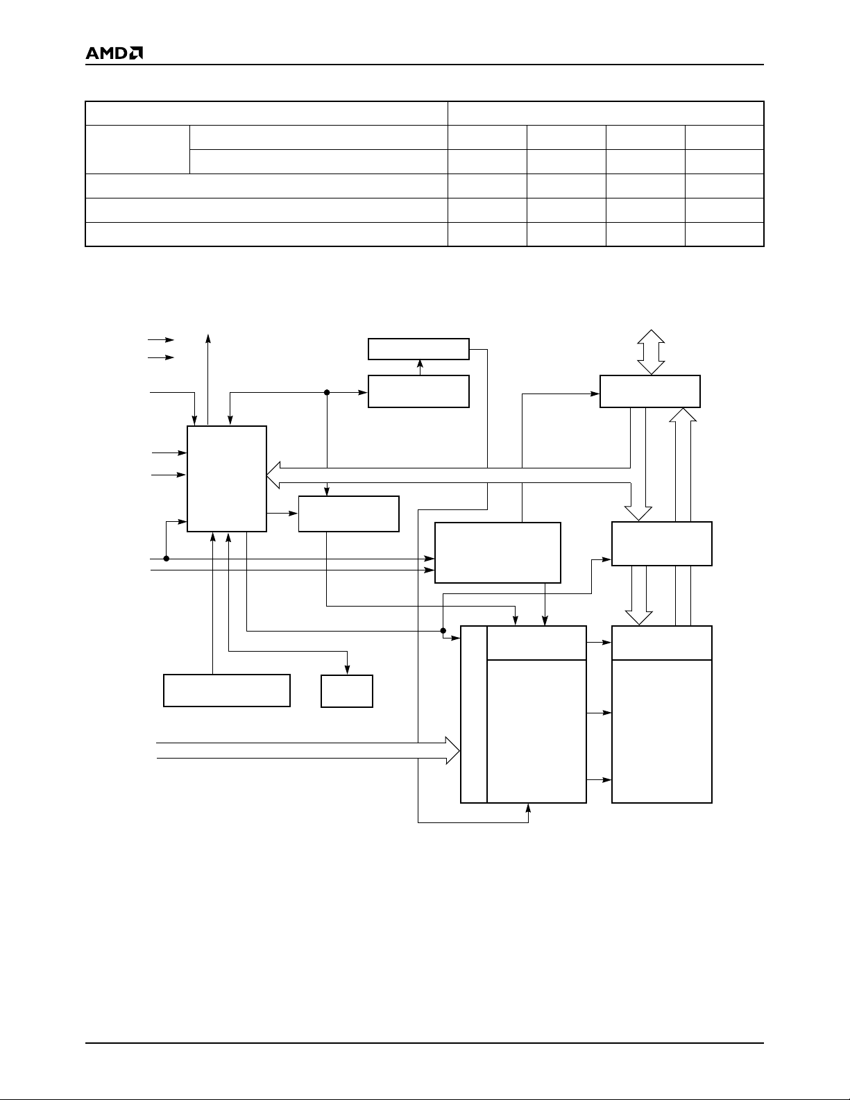
BLOCK DIAGRAM
DQ0
DQ15 (A-1)
–
Input/Output
Buffers
Data
Latch
V
CC
V
SS
RESET#
WE#
BYTE#
CE#
OE#
RY/BY#
State
Control
Command
Register
PGM Voltage
Generator
Sector Switches
Erase Voltage
Generator
Chip Enable
Output Enable
Logic
STB
A0–A17
VCC Detector
Timer
STB
Address Latch
Y-Decoder
X-Decoder
Y-Gating
Cell Matrix
21523A-1
3 Am29LV400B
Page 4

CONNECTION DIAGRAMS
ADVANCE INFORMATION
A15
A14
A13
A12
A11
A10
A9
A8
NC
NC
WE#
RESET#
NC
NC
RY/BY#
NC
A17
A7
A6
A5
A4
A3
A2
A1
A16
BYTE#
V
DQ15/A-1
DQ7
DQ14
DQ6
DQ13
DQ5
DQ12
DQ4
V
DQ11
DQ3
DQ10
DQ2
DQ9
DQ1
DQ8
DQ0
OE#
V
CE#
SS
CC
SS
A0
1
2
3
4
5
6
7
8
9
10
11
12
13
14
15
16
17
18
19
20
21
22
23
24
1
2
3
4
5
6
7
8
9
10
11
12
13
14
15
16
17
18
19
20
21
22
23
24
Standard TSOP
Reverse TSOP
48
47
46
45
44
43
42
41
40
39
38
37
36
35
34
33
32
31
30
29
28
27
26
25
48
47
46
45
44
43
42
41
40
39
38
37
36
35
34
33
32
31
30
29
28
27
26
25
A16
BYTE#
V
SS
DQ15/A-1
DQ7
DQ14
DQ6
DQ13
DQ5
DQ12
DQ4
V
CC
DQ11
DQ3
DQ10
DQ2
DQ9
DQ1
DQ8
DQ0
OE#
V
SS
CE#
A0
A15
A14
A13
A12
A11
A10
A9
A8
NC
NC
WE#
RESET#
NC
NC
RY/BY#
NC
A17
A7
A6
A5
A4
A3
A2
A1
21523A-2
1/29/98 Am29LV400B 4
Page 5

CONNECTION DIAGRAMS
ADVANCE INFORMATION
NC
RY/BY#
A17
A7
A6
A5
A4
A3
A2
A1
A0
CE#
V
SS
OE#
DQ0
DQ8
DQ1
DQ9
DQ2
DQ10
DQ3
DQ11
10
11
12
13
14
15
16
17
18
19
20
21
22
1
2
3
4
5
6
7
8
9
SO
44
43
42
41
40
39
38
37
36
35
34
33
32
31
30
29
28
27
26
25
24
23
RESET#
WE#
A8
A9
A10
A11
A12
A13
A14
A15
A16
BYTE#
V
SS
DQ15/A-1
DQ7
DQ14
DQ6
DQ13
DQ5
DQ12
DQ4
V
CC
Bump Side (Bottom) View
FBGA
A1 B1 C1 D1 E1 F1 G1 H1
CE#A0A1A2A4A3
OE# V
SS
A2 B2 C2 D2 E2 F2 G2 H2
DQ9 DQ1DQ8DQ0A5A6A17A7
A3 B3 C3 D3 E3 F3 G3 H3
DQ11 DQ3DQ10DQ2NCNCNCRY/BY#
A4 B4 C4 D4 E4 F4 G4 H4
V
CC
DQ4DQ12DQ5NCNCRESET#WE#
A5 B5 C5 D5 E5 F5 G5 H5
DQ13 DQ6DQ14DQ7A11A10A8A9
A6 B6 C6 D6 E6 F6 G6 H6
BYTE#A16A15A14A12A13
DQ15/A-1 V
SS
5 Am29LV400B
21523A-3
Page 6

ADVANCE INFORMATION
Special Handling Instructions for Fine
PItch Ball Grid Array (FBGA)
Special handling is required for Flash Memory products
in FBGA packages.
PIN CONFIGURATION
A0–A17 = 18 addresses
DQ0–DQ14 = 15 data inputs/outputs
DQ15/A-1 = DQ15 (data input/output, word mode),
A-1 (LSB address input, byte mode)
BYTE# = Selects 8-bit or 16-bit mode
CE# = Chip enable
OE# = Output enable
WE# = Write enable
RESET# = Hardware reset pin, active low
RY/BY# = Ready/Busy# output
= 3.0 volt-only single power s upply
V
CC
(see Product Selector Guide for speed
options and voltage supply toleranc es)
Flash memory devices in FBGA packages may be
damaged if exposed to ultrasonic cleaning methods.
The package and/or data integrity may be
compromised if the package bod y is ex posed to
temperatures above 150°C for prolonged periods of
time.
LOGIC SYMBOL
18
A0–A17
DQ0–DQ15
(A-1)
CE#
OE#
WE#
RESET#
BYTE# RY/BY#
16 or 8
21523A-4
V
SS
= Device ground
NC = Pin not connected internally
1/29/98 Am29LV400B 6
Page 7

ADVANCE INFORMATION
ORDERING INFORMATION
Standard Pr od ucts
AMD standard products are available in s everal packages and operating ranges. The order number (Valid Combination) is formed by a combination of the elements below.
CE70RAm29LV400B T
OPTIONAL PROCESSING
Blank = Standard Processing
B = Burn-in
(Contact an AMD representative for more information)
TEMPERATURE RANGE
C=Commercial (0°C to +70°C)
I = Industrial (–40°C to +85°C)
E = Extended (–55°C to +125°C)
PACKAGE TYPE
E = 48-Pin Thin Small Outline Package (TSOP)
Standard Pinout (TS 048)
F = 48-Pin Thin Small Outline Package (TSOP)
Reverse Pinout (TSR048)
S = 44-Pin Small Outline Package (SO 044)
WA = 48-ball Fine Pitch Ball Grid Array (FBGA)
0.80 mm pitch, 6 x 8 mm package
SPEED OPTION
See Product Selector Guide and Valid Combinations
BOOT CODE SECTOR ARCHITECTURE
T = Top Sector
B = Bottom Sector
DEVICE NUMBER/DESCRIPTION
Am29LV400B
4 Megabit (512 K x 8-Bit/256 K x 16-Bit) CMOS Flash Memory
3.0 Volt-only Read, Program, and Erase
Valid Combinations
Valid Combinations
Am29LV400BT70R,
Am29LV400BB70R
Am29LV400BT80,
Am29LV400BB80
Am29LV400BT90,
Am29LV400BB90
Am29LV400BT120,
Am29LV400BB120
Trademarks
Copyright © 1998 Advanced Micro Devices, Inc. All rights reserved.
AMD, the AMD logo, and combinations thereof are registered trademarks of Advanced Micro Devices, Inc.
ExpressFlash is a trademark of Advanced Micro Devices, Inc.
Product names used in this publication are for identification purposes only and may be trademarks of their respective companies.
EC, EI, FC,
FI, SC, SI, WAC
EC, EI, EE,
FC, FI, FE,
SC, SI, SE,
WAC, WAI, WAE
Valid Combinations list configurations planned to be supported in volume for this device. Consult the local AMD sales
office to confirm availability of specific valid combinations and
to check on newly released combinations.
7 Am29LV400B
 Loading...