

Datasheet AM29F800BT-90DPC1, AM29F800BT-90DGI1, AM29F800BT-90DGC1, AM29F800BT-120DGE1, AM29F800BT-120DGC1 Datasheet (AMD Advanced Micro Devices)
...Page 1

SUPPLEMENT
Am29F800B Known Good Die
8 Megabit (1 M x 8-Bit/512 K x 16-Bit)
CMOS 5.0 Volt-only, Boot Sector Flash Memory—Die Revision 1
DISTINCTIVE CHARACTERISTICS
■ Single power supply operation
— 5.0 Volt-only operation for read, erase, and
program operations
— Minimizes system level requirements
■ Manufactured on 0.35 µm process technology
— Compatible with 0.5 µm Am29F800 device
■ High performance
— 90 or 120 ns access time
■ Low power consumption (typical values at 5
MHz)
—1 µA standby mode current
— 20 mA read current (byte mode)
— 28 mA read current (word mode)
— 30 mA program/erase current
■ Flexible sector architecture
— One 16 Kbyte, two 8 Kbyte, one 32 Kbyte, and
fifteen 64 Kbyte sectors (byte mode)
— One 8 Kword, two 4 Kword, one 16 Kword, and
fifteen 32 Kword sectors (word mode)
— Supports full chip erase
— Sector Protection features:
A hardware method of locking a sector to
prevent any program or erase operations within
that sector
Sectors can be locked via programming
equipment
T emporary Sector Unprotect feat ure allows code
changes in previously locked sectors
■ Top or bottom boot block configurations
available
■ Embedded Al gorithms
— Embedded Erase algorithm automatically
preprograms and erases the entire chip or any
combination of designated sectors
— Embedded Program algorithm automatically
writes and verifies data at specified addresses
■ Minimum 1,000,000 write cycles per sector
guaranteed
■ Compatibility with JEDEC standards
— Pinout and software compatible with single-
power-supply Flash
— Superior inadvertent write protection
■ Data# Polling and toggle bits
— Provides a software method of detecting
program or erase operation completion
■ Ready/Busy# pin (RY/BY#)
— Provides a hardware method of detecting
program or erase cycle completion
■ Erase Suspend/Erase Resume
— Suspends an erase operati on to read dat a from,
or program data to, a sector that is not being
erased, then resumes the erase operation
■ Hardware reset p in (RESET#)
— Hardware method to reset the de vice t o reading
array data
5/4/98
Publication# 21631 Rev: A Amendment/+2
Issue Date: April 1998
Page 2

SUPPLEMENT
GENERAL DESCRIPTION
The Am29F800B in Known Good Die (KGD) form is a
8 Mbit, 5.0 volt-only Flash memory. AMD defines KGD
as standard product in die form, tested for functionality
and speed. AMD KGD products have the same reliability and quality as AMD products in packaged form.
Am29F800B Features
The Am29F800B is an 8 Mbit, 5.0 volt-only Flas h
memory organized as 1,048,576 bytes or 524,288
words. The word-wide data (x16) appears on
DQ15–DQ0; the byte-wide (x8) data appears on
DQ7–DQ0. This device is designed to be programmed
in-system with the standard system 5.0 volt V
supply. A 12.0 V VPP is not required for write or erase
operations. The device can also be programmed in
standard EPROM programmers.
This device is manufactured using AMD’s 0.35 µm
process technology, and off ers all the f eatures and benefits of the Am29F800, which was manufactured using
0.5 µm process technology.
CC
before e xecuting the er ase operation. During erase, the
device automatically times the erase pulse widths and
verifies proper cell margin.
The host system can detect whether a program or
erase operation is complete by obser ving the RY/BY#
pin, or by reading the DQ7 (Data# Polling) and DQ6
(toggle) status bits. After a program or erase cycle has
been completed, the device is ready to read array data
or accept another command.
The sector erase archite cture allo ws m emory sect ors
to be erased and reprogrammed without affecting the
data contents of other sectors. The device is fully
erased when shipped from the factory.
Hardware data protection measures include a low
detector that automatically in hibits write opera-
V
CC
tions during power transitions. The hardware sector
protection feature disables both program and erase
operations in any combination of the sectors of memory . This can be achie v ed via prog ramming equipment.
To eliminate bus contention the device has separate
chip enable (CE#), write enable (WE#) and output
enable (OE#) controls.
The device requires only a single 5. 0 v o lt po wer sup-
ply for both read and wr ite functions. Internally generated and regulated voltages are provided for the
program and erase operations.
The device is entirely command set compatible with the
JEDEC single-power-supply Flash standard. Commands are written to the command regis ter using
standard micropr ocessor wri te timings. Register co ntents serve as input to an internal state-machine that
controls the erase and programming circuitry. Write
cycles also internally latch addresses and data needed
for the programming and erase operations. Reading
data out of the device is similar to reading from other
Flash or EPROM devices.
Device programming occurs by executing the program
command sequence. This initiates the Embedded
Program algorithm—an internal algorithm that automatically times the program pulse widths and verifies
proper cell margin.
Device erasure occurs by executing the erase command sequence. This initiates the Embedded Erase
algorithm—an in ternal algorithm that autom atically
preprograms the array (if it is not already prog rammed)
The Erase Suspend feature enables the user to put
erase on hold for any period of time to read data from,
or program data to, any s ector that is not selected for
erasure. True background erase can thus be achie ved.
The hardware RESET# pi n terminates any operation
in progress and resets the internal state machine to
reading array dat a. The RESET# pin ma y be tied to the
system reset circuitry. A system reset would thus also
reset the device, enabling the system microprocessor
to read the boot-up firmware from the Flash memory.
The system can place the device into the standby
mode. Power consum ption is greatly reduced in
this mode.
AMD’s Flash technology combines years of Flash
memory manufacturing experience to produce the
highest levels of quality, reliability and cost
effectiveness. The device electrically erases al l
bits within a sector simultaneously via
Fowler-Nordheim tunneling. The data is
programmed using hot electron injection.
ELECTRICAL SPECIFICATIONS
Refer to the Am29F800B data sheet, PID 21504, for full
electrical specifications on the Am29F800B in KGD
for m .
2 Am29F800B Known Good Die 5/4/98
Page 3
SUPPLEMENT
PRODUCT SELECTOR GUIDE
Family Part Number Am29F800B KGD
Speed Option (V
Max access time, ns (t
= 5.0 V ± 10%) -90 -120
CC
) 90 120
ACC
Max CE# access time, ns (tCE) 90 120
Max OE# access time, ns (tOE) 35 50
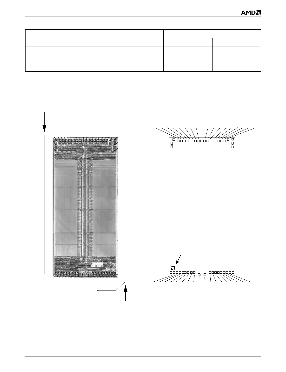
DIE PHOTOGRAPH DIE PAD LOCATIONS
Orientation relative
to leading edge of
tape and reel
9876543214443424140393837
10
11
12
36
35
34
33
AMD logo loca tio n
13
2120191817161514
22
Orientation relative
to top left corner of
Gel-Pak
5/4/98 Am29F800B Known Good Die 3
32
313029282726252423
Page 4

SUPPLEMENT
PAD DESCRIPTION
Pad Signal
1V
2 DQ4 7.22 0.00 0.1835 0.0000
3 DQ12 13.45 0.00 0.3417 0.0000
4 DQ5 19.59 0.00 0.4977 0.0000
5 DQ13 25.82 0.00 0.6559 0.0000
6 DQ6 31.96 0.00 0.8119 0.0000
7 DQ14 38.19 0.00 0.9701 0.0000
8 DQ7 44.33 0.00 1.1261 0.0000
9 DQ15/A-1 50.56 0.00 1.2843 0.0000
10 V
11 BYTE# 60.50 6.84 1.5367 0.1738
12 A16 60.50 18.99 1.5367 0.4823
13 A15 60.13 279.88 1.5274 7.1090
14 A14 53.99 279.88 1.3714 7.1090
15 A13 48.28 279.88 1.2264 7.1090
16 A12 42.14 279.88 1.0704 7.1090
17 A11 36.43 279.88 0.9254 7.1090
18 A10 30.29 279.88 0.7694 7.1090
19 A9 24.58 279.62 0.6244 7.1024
20 A8 18.34 279.88 0.4659 7.1090
21 WE# 12.63 279.88 0.3209 7.1090
22 RESET# 2.54 283.85 0.0646 7.2098
23 RY/BY# –10.00 283.85 –0.2538 7.2098
24 A18 –20.07 279.88 –0.5096 7.1090
25 A17 –25.78 279.88 –0.6546 7.1090
26 A7 –31.92 279.88 –0.8106 7.1090
27 A6 –37.63 279.88 –0.9556 7.1090
28 A5 –43.77 279.88 –1.1116 7.1090
29 A4 –49.48 279.88 –1.2566 7.1090
30 A3 –55.62 279.88 –1.4126 7.1090
31 A2 –61.33 279.88 –1.5576 7.1090
32 A1 –67.47 279.88 –1.7136 7.1090
33 A0 –67.84 18.99 –1.7229 0.4823
34 CE# –67.84 6.84 –1.7229 0.1738
35 V
36 OE# –57.84 –2.39 –1.4691 –0.0608
37 DQ0 –49.86 0.00 –1.2661 0.0000
38 DQ8 –43.63 0.00 –1.1082 0.0000
39 DQ1 –37.49 0.00 –0.9522 0.0000
40 DQ9 –31.26 0.00 –0.7940 0.0000
41 DQ2 –25.12 0.00 –0.6380 0.0000
42 DQ10 –18.89 0.00 –0.4798 0.0000
43 DQ3 –12.75 0.00 –0.3238 0.0000
44 DQ11 –6.52 0.00 –0.1656 0.0000
CC
SS
SS
–67.84 –4.00 –1.7229 –0.1015
Note: The coordinates above are relative to the center of pad 1 and can be used to operate wire bonding equipment.
Pad Center (mils) Pad Center (millimeters)
XYXY
0.00 0.00 0.0000 0.0000
58.61 –1.42 1.4887 –0.0361
4 Am29F800B Known Good Die 5/4/98
Page 5

SUPPLEMENT
ORDERING INFORMATION
Standard Pr od ucts
AMD standard products are available in several packages and operating ranges. The order number (Valid Combination) is
formed by a combination of the following:
Am29F800B
T
-90
DP
C
1
DIE REVISION
This number refers to the specific AMD manufacturing
process and product technology reflected in this document. It is entered in the revision field of AMD standard product nomenclature.
TEMPERATURE RANGE
C = Commercial (0°C to +70°C)
I = Industrial (–40°C to +85°C)
E = Extended (–55°C to +125°C)
PACKAGE TYPE AND
MINIMUM ORDER QUANTITY
DP = Waffle Pack
DG = Gel-Pak
DT = Surft ape ™ (Ta pe and Reel)
DW = Gel-Pak
Call AMD sales office for minimum order quantity
SPEED OPTION
See Valid Combinations
BOOT CODE SECTOR ARCHITECTURE
T = Top sector
B = Bottom sector
180 die per 5 tray stack
®
378 die per 6 tray stack
1800 per 7-inch reel
Die Tray
®
Wafer Tray (sawn wafer on frame)
Am29F800BT-90,
Am29F800BB-90,
Am29F800BT-120
Am29F800BB-120
Valid Combinations
DPC 1, DPI 1, DPE 1,
DGC 1, DGI 1, DGE 1,
DTC 1, DTI 1, DTE 1,
DWC 1, DWI 1, DWE 1
DEVICE NUMBER/DESCRIPTION
Am29F800B Known Good Die
8 Megabit (1 M x 8-Bit/512 K x 16-Bit) CMOS Flash Memory—Die Revision 1
5.0 Volt-only Program and Erase
Valid Combinations
Valid Combinations list configurations planned to be supported in volume for this device. Consult the local AMD sales
office to confirm availability of specific valid combinations and
to check on newly released combinations.
5/4/98 Am29F800B Known Good Die 5
Page 6

SUPPLEMENT
PRODUCT TEST FLOW
Figure 1 provides an overview of AMD’s Known Good
Die test flow . F or more detailed inf ormation, ref er to the
Am29F800B product qualification database supplement for KGD . AMD implements quality assurance procedures throughout the product test flow. In addition,
Wafer Sort 1
an off-line quality monitoring program (QMP) fur ther
guarantees AMD quality standards are met on Known
Good Die products. These QA procedures also allow
AMD to produce KGD products without requiring or
implementing burn-in.
DC Parameters
Functionality
Programmability
Erasability
Bake
24 hours at 250°C
Wafer Sort 2
Wafer Sort 3
High Temperature
Packaging for Shipment
Data Retention
DC Parameters
Functionality
Programmability
Erasability
DC Parameters
Functionality
Programmability
Erasability
Speed
Incoming Inspection
Wafer Saw
Die Separation
100% Visual Inspection
Die Pack
Shipment
Figure 1. AM D KGD P roduct Test Flow
6 Am29F800B Known Good Die 5/4/98
Page 7

SUPPLEMENT
PHYSICAL SPECIFICATIONS
Die dimensions . . . . . . . . . 141.34 mils x 306.30 mils
. . . . . . . . . . . . . . . . . . . . . . . . . . .3.59 mm x 7.78 mm
Die Thickness. . . . . . . . . . . . . . . . . . . . . . . . . ~20 mils
Bond Pad Size . . . . . . . . . . . . . . 3.94 mils x 3.94 mils
. . . . . . . . . . . . . . . . . . . . . . . . . . . . .100 µm x 100 µm
Pad Area Free of Passivation . . . . . . . . . .15.52 mils
. . . . . . . . . . . . . . . . . . . . . . . . . . . . . . . . . 10,000 µm
Pads Per Die . . . . . . . . . . . . . . . . . . . . . . . . . . . . . .44
Bond Pad Metalization. . . . . . . . . . . . . . . . . . Al/Cu/Si
Die Backside . . . . . . . . . . . . . . . . . . . . . . . . No metal,
may be grounded (optional)
Passivation. . . . . . . . . . . . . . . . . . Nitride/SOG/Nitride
DC OPERATING CONDITIONS
VCC (Supply Voltage) . . . . . . . . . . . . . . .4.5 V to 5.5 V
Junction Temperature Under Bias . .T
Operating Temperature
Commercial . . . . . . . . . . . . . . . . . . . 0°C to +70°C
Industrial . . . . . . . . . . . . . . . . . . . –40°C to +85°C
Extended . . . . . . . . . . . . . . . . . . –55°C to +125°C
(max) = 130°C
J
MANUFACTURING INFORMATION
Manufacturing . . . . . . . . . . . . . . . . . . . . . . . . . . FASL
Test . . . . . . . . . . . . . . . . . . . . . . . . . . . . . . . . . . . SDC
Manufacturing ID (Top Boot) . . . . . . . . . . . .98924AK
(Bottom Boot) . . . . . . . .98924ABK
Preparation for Shipment . . . . . . . . Penang, Malaysia
2
Fabrication Process . . . . . . . . . . . . . . . . . . . . . .CS39
2
Die Revision . . . . . . . . . . . . . . . . . . . . . . . . . . . . . . . 1
SPECIAL HANDLING INSTRUCTIONS
Processing
Do not expose KGD products to ultraviolet light or
process them at temperatures greater than 250°C.
Failure to adhere to these handling instr uctions will
result in irre parable damage to th e devices. For best
yield, AMD recommends assembly in a Class 10K
clean room with 30% to 60% relative humidity.
Storage
Store at a maximum temper ature of 30° C in a nitrogenpurged cabinet or vacuum-sealed bag. Observe all
standard ESD handling procedures.
5/4/98 Am29F800B Known Good Die 7
Page 8

SUPPLEMENT
TERMS AND CONDITIONS OF SALE FOR AMD NON-VOLATILE MEMORY DIE
All transactions relating to AMD Products under this
agreement shall be subject to AMD’s standard terms
and conditions of sale, or any revisions thereof, which
revisions AMD reserves the right to make at any time
and from time to time. In the event of conflict between
the provisions of AMD’s standard terms and conditions
of sale and this agreement, the terms of this ag reement
shall be controlling.
AMD warrants a rticles of i ts manufacture against
defective materials or workmanship for a period of
ninety (90) days from date of shipment. This warranty
does not extend be yond AMD’ s cust omer , and does not
extend to die which has been affixed onto a board or
substrate of any kin d. The liability o f AMD under th is
warranty is limited, at AMD’s option, solely to repair or
to replacement with equivalent articles, or to make an
appropriate credit adjustment not to ex ceed the original
sales price, for articles returned to AMD , pro vided that :
(a) The Buyer promptly notifies AMD in writing of each
and every defect or nonconformity in any article for
which Buyer wishes to make a warranty claim against
AMD; (b) Buyer obtains authorization from AMD to
return the ar ticle; (c) the ar ticle is returned to AMD,
transportation charges paid by AMD, F.O.B. A MD’ s f actory; and (d) AM D’s examination of such article discloses to its satisfactio n that such alleged defect or
nonconformity actually exists and was not caused by
negligence, misuse, improper installation, accident or
unauthorized repair or alteration by an entit y other than
AMD. The af orementioned prov isions do not e xtend the
original warranty period of any article which has either
been repaired or replaced by AMD.
THIS WARRANTY IS EXPRESSED IN LIEU OF ALL
OTHER WARRANTIES, EXPRESSED OR IMPLIED,
INCLUDING THE IMPLIED W ARRANT Y OF FITNESS
FOR A PARTICULAR PURPOSE, THE IMPLIED
WARRANTY O F MERCHANTABILITY AND OF ALL
OTHER OBLIGATIONS OR LIABILITIES ON AMD’S
PART, AND IT NEITHER ASSUMES NOR AUTHORIZES ANY OTHER PERSON TO ASSUME FOR AMD
ANY OTHER LIABILITIES. THE FOREGOING CON STITUTES THE BUYERS SOLE AND EXCLUSIVE
REMEDY FOR THE FURNISHING OF DEFECTIVE
OR NON CONFORMING ARTICLES AND AMD
SHALL NOT IN ANY EVENT BE LIABLE FOR
DAMAGES BY REASON OF FAILURE OF ANY
PRODUCT TO FUNCTION PROPERLY OR FOR ANY
SPECIAL, INDIRECT, CONSEQUENTIAL, INCIDENTAL OR EXEMPLARY DAMAGES, INCLUD ING
BUT NOT LIMITE D TO , LOSS OF PROFIT S, LOSS OF
USE OR COST OF LABOR BY REASON OF THE
FACT TH AT SUCH ARTICLES SHALL HAVE BEEN
DEFECTIVE OR NON CONFORMING.
Buyer agrees that it will make no warranty representations to its customers which exceed those given by
AMD to Buyer unless and until Buyer shall agree to
indemnify AMD in writing for any claims which exc eed
AMD’s warranty. Buyer assumes all responsibility for
successful die prep, die attach and wire bonding processes. Due to the unprotected nature of the AMD Products which are th e subject hereof, AMD assu mes no
responsibility for environmental effects on die.
AMD products are not designed or author ized for use
as components in life support appliances, devices or
systems where malfunction of a product can reasonably be expec ted to result in a personal injury. Buyer’s
use of AMD products for u se in lif e support applications
is at Buyer’s own risk and Buyer agrees to fully indemnify AMD for any damages resulting in s uch use or sale.
8 Am29F800B Known Good Die 5/4/98
Page 9

SUPPLEMENT
REVISION SUMMARY FOR AM29F800B KGD
Revision A+1, A+2
Distinctive Characteristics
Changed typical program/erase t ime to 30 mA to match
the CMOS DC Characteristics table in the Am29F400B
full data sheet.
The minimum guarante per sector is now 1 million
cycles.
Pad Description
Corrected the following dimensions:
X (mils): pads 15, 18, 36
Y (mils): pads 10–12, 35, 36
X (mm): pads 2–22, 37, 38
Y (mm): pads 10–12, 23–32, 35, 36
Physical Specifications
Changed die thickness specification to ~20 mils.
Trademarks
Copyright © 1998 Advanced Micro D evices, Inc. All rights reserved.
AMD, the AMD logo, and combinations thereof are registered trademarks of Advanced Micro Devices, Inc.
Product names used in this publication are for identification purposes only and may be trademarks of their respective companies.
5/4/98 Am29F800B Known Good Die 9
 Loading...