

Datasheet AM29F016B-120DWI1, AM29F016B-120DTI1, AM29F016B-120DTC1, AM29F016B-120DPI1, AM29F016B-120DPC1 Datasheet (AMD Advanced Micro Devices)
...Page 1

SUPPLEMENT
Am29F016B Known Good Die
16 Megabit (2 M x 8-Bit)
CMOS 5.0 Volt-only, Sector Erase Flash Memory—Die Revision 1
DISTINCTIVE CH AR ACTERISTICS
■ 5.0 V ± 10%, single power supply operation
— Minimizes system level power requirements
■ Manufactured on 0.35 µm process technology
■ High performance
— 120 ns access time
■ Low power consumption
— 25 mA typical active read current
— 30 mA typical program/erase current
—<1 µA typical standby current (standard access
time to active mode)
■ Flexible sector architecture
— 32 uniform sectors of 64 Kbytes each
— Any combination of sectors can be erased.
— Supports full chip erase
— Group sector protection:
A hardware method of locking sector groups to
prevent any program or erase operations within
that sector group
Temporary Sector Group Unprotect allows code
changes in previously locked sectors
■ Embedded Algorithms
— Embedded Erase algorithm automatically
preprograms and erases the entire chip or any
combination of designated sectors
— Embedded Program algorithm automatically
writes and verifies bytes at specified addresses
■ Minimum 100,000 write/erase cyc les guaranteed
■ Compatible with JEDEC standards
— Pinout and software compatible with
single-power-supply Flash standard
— Superior inadvertent write protection
■ Data# Polling and toggle bits
— Provides a software method of detecting
program or erase cycle completion
■ Ready/Busy output (RY/BY#)
— Provides a hardware method for detecting
program or erase cycle completion
■ Erase Suspend/Resume
— Suspends a sector erase operation to read data
from, or program data to, a non-erasing sector,
then resumes the erase operation
■ Hardware reset pin (RESET#)
— Resets internal state machine to the read mode
■ Tested to datasheet specifications at
temperature
■ Quality and reliability levels equivalent to
standard packaged components
2/17/98 Publication# 21551 Rev: A Amendment/+1
Issue Date: February 1998
Page 2
SUPPLEMENT
GENERAL DESCRIPTION
The Am29F016B in Known Good Die (KGD) form is a
16 Mbit, 5.0 volt-only Flash memory . AMD defines KGD
as standard product in die form, tested for functionality
and speed. AMD KGD products have the same reliability and quality as AMD products in packaged form.
The sector erase architecture allows memory sectors
to be erased and reprogrammed without affecting the
data contents of other sectors. A sector is typically
erased and verified within one second. The device is
erased when shipped from the factory.
Am29F016B Features
The Am29F016B is a 16 Mbit, 5.0 volt-only Flash
memory organized as 2,097,152 bytes of 8 bits each.
The 2 Mbytes of data are divided into 32 sectors of 64
Kbytes each for flexible erase capability. The 8 bits of
data appear on DQ0–DQ7. The Am29F016B is manufactured using AMD’s 0.35 µm process technology.
This device is designed to be programmed in-system
with the standard system 5.0 volt V
volt V
is not required for program or erase
PP
operations. The dev ice can also be programmed in
standard EPROM programmers.
The standard device offers an access time of 120 ns,
allowing high-speed microprocessors to operate
without wait states. To eliminate bus contention, the
device has separate chip enable (CE#), w rite enable
(WE#), and output enable (OE#) controls.
The device is entirely command set compatible with the
JEDEC single -power-supply Flash standar d. Commands are written to the command register using
standard microprocessor write timings. Register
contents serve as input to an internal state machine
that controls the erase and programming circuitry.
Write cycles also internally lat ch addresses and data
needed for the programming and erase operations.
Reading data out of the device is similar to reading
from 12.0 volt Flash or EPROM devices.
The device is programmed by executing the program
command sequence. This invokes the Embedded
Program algorithm—an inter nal algorithm that a utomatically times the program pulse widths and verifies
proper cell margin. The device is erased by executing
the erase command sequence. This invokes the
Embedded Erase algorithm—an internal algorithm that
automatically preprograms the array (if it is not already
programmed) before executing the erase operation.
During erase, the device automatically times the erase
pulse widths and verifies proper cell margin.
supply. A 12. 0
CC
The hardware sector group protection feature disables
both program and erase operations in an y combination
of the eight sector groups of memory. A sector group
consists of four adjacent sectors.
The Erase Suspend feature enables the system to put
erase on hold for any period of time to read data from,
or program data to, a sector that is not being erased.
True background erase can thus be achieved.
The device requires only a single 5.0 volt po wer supply
for both read and write functions. Internally generated
and regulated voltages are provided for the program
and erase operations. A low V
detector automatically
CC
inhibits write operations during power transitions. The
host system can detect whether a program or erase
cycle is complete by using the RY/BY# pin, the DQ7
(Data# Polling) or DQ6 (toggle) status bits. After a
program or erase cycle h as been completed, the
device automatically returns to the read mode.
A hardware RESET# pin te rminates any ope ration in
progress. The internal stat e machine is reset to the
read mode. The RESET# pin may be tied to the system
reset circuitry. Therefore, if a system reset occurs
during either an Embedded Program or Embedded
Erase algorithm, the device is automatically reset to the
read mode. This enables the system’s microprocessor
to read the boot-up firmware from the Flash memory.
AMD’s Flash technology combines years of Flash
memory manufacturing experience to produce the
highest levels of quality, reliability, and cost
effectiveness. The device electrically erases all bits
within a sector simultaneously via Fowler-Nordheim
tunneling. The bytes are programmed one byte at a
time using the EPROM programming mechanism of hot
electron injection.
ELECTRICAL SPECIFICATIONS
Refer to the Am29F016B data sheet, PID 21444, for full
electrical specifications on the Am29F016B in KGD
form.
PRODUCT SELECTOR GUIDE
Family Part Number Am29F016B KGD
Speed Option (VCC = 5.0 V ± 10%) -120
Max Access Time, t
Max CE# Access, tCE (ns) 120
Max OE# Access, t
2 Am29F016B Known Good Die 2/17/98
(ns) 120
ACC
(ns) 50
OE
Page 3
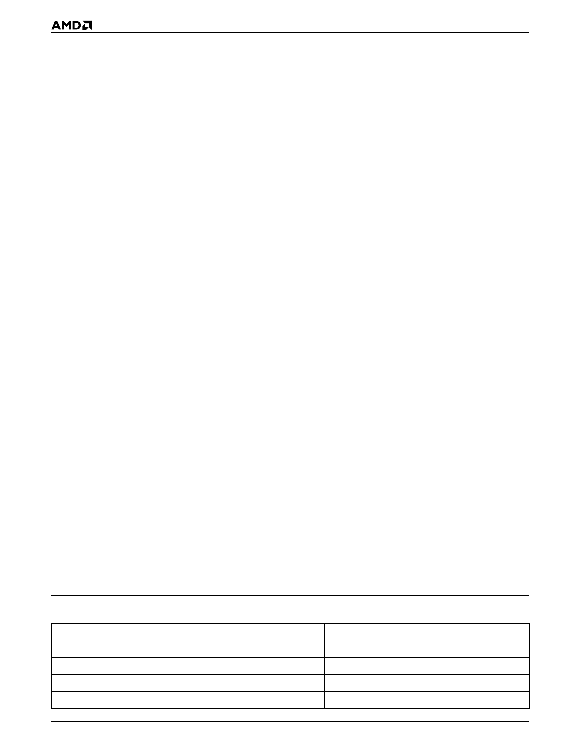
DIE PHOTOGRAPH
Orientation
relative to top
left corner of
Gel-Pak
SUPPLEMENT
Orientation relative
to leading edge of
tape and reel
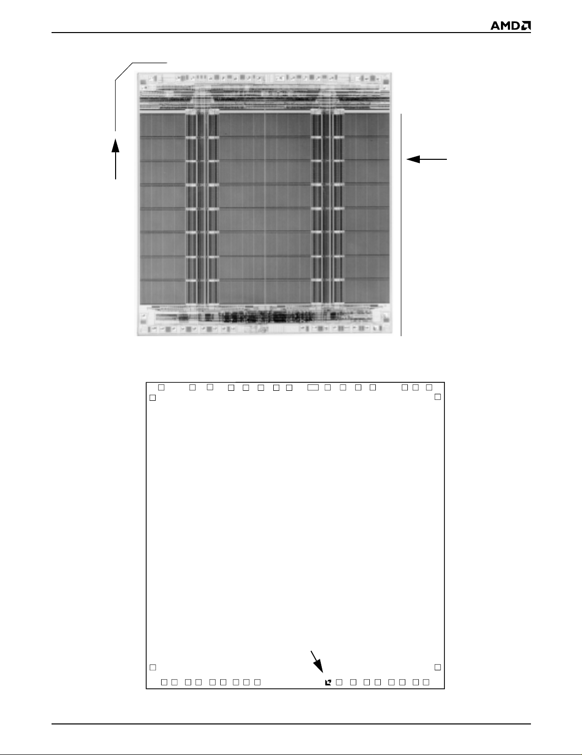
DIE PAD LOCATIONS
9
12345678
AMD logo location
31353637 323334
30
29
10
1112 13 14 15 16 17 19 20 21 22 23 24 25 26 27
18
28
2/17/98 Am29F016B Known Good Die 3
Page 4

SUPPLEMENT
PAD DESC RIPTION
Pad Signal
1V
CC
2DQ4–10.60 0.00 –0.27 0.00
3 DQ5 –24.00 0.00 –0.61 0.00
4 DQ6 –37.20 0.00 –0.94 0.00
5 DQ7 –50.50 0.00 –1.28 0.00
6 RY/BY# –68.90 0.00 –1.75 0.00
7 OE# –84.20 0.00 –2.14 0.00
8 WE# –111.80 0.00 –2.84 0.00
9 A20 –119.30 –8.50 –3.03 –0.22
10 A19 –119.30 –245.30 –3.03 –6.23
11 A18 –109.10 –258.20 –2.77 –6.56
12 A17 –100.20 –258.20 –2.55 –6.56
13 A16 –88.20 –258.20 –2.24 –6.56
14 A15 –79.00 –258.20 –2.01 –6.56
15 A14 –67.00 –258.20 –1.70 –6.56
16 A13 –57.80 –258.20 –1.47 –6.56
17 A12 –45.80 –258.20 –1.16 –6.56
18 CE# –36.60 –258.20 –0.93 –6.56
19 V
CC
20 RESET# 45.00 –258.20 1.14 –6.56
21 A11 57.20 –258.20 1.45 –6.56
22 A10 69.20 –258.20 1.76 –6.56
23 A9 78.40 –258.20 1.99 –6.56
24 A8 90.60 –258.20 2.30 –6.56
25 A7 99.80 –258.20 2.53 –6.56
26 A6 112.00 –258.20 2.84 –6.56
27 A5 121.10 –258.20 3.08 –6.56
28 A4 131.20 –245.30 3.33 –6.23
29 A3 131.20 –8.50 3.33 –0.22
30 A2 123.80 0.00 3.14 0.00
31 A1 111.90 0.00 2.84 0.00
32 A0 102.40 0.00 2.60 0.00
33 DQ0 74.40 0.00 1.89 0.00
34 DQ1 61.20 0.00 1.55 0.00
35 DQ2 47.90 0.00 1.22 0.00
36 DQ3 34.70 0.00 0.88 0.00
37 V
SS
Note: The coordinates above are relative to the center of pad 1 and can be used to operate wire bonding equipment.
Pad Center (mils) Pad Center (millimeters)
XYXY
0.00 0.00 0.00 0.00
–27.20 –258.20 –0.69 –6.56
21.70 0.00 0.55 0.00
4 Am29F016B Known Good Die 2/17/98
Page 5

SUPPLEMENT
ORDERING INFORMATION
Standard Products
AMD standard products are available in sev eral packages and operat ing ranges. The or der number (Valid Combin ation) is
formed by a combination of the following:
Am29F016B
-120
DP
C
1
DIE REVISION
This number refers to the specific AMD manufacturing
process and product technology reflected in this
document. It is entered in the revision field of AMD
standard product nomenclature.
TEMPERATURE RANGE
C = Commercial (0°C to +70°C)
I = Industrial (–40°C to +85°C)
PACKAGE TYPE AND
MINIMUM ORDER QUANTIT Y
DP = Waffle Pack
100 die per 5 tray stack
DG = Gel-Pak
294 die per 6 tray stack
DT = Surftape™ (Tape and Reel)
1600 per 7-inch reel
DW = Gel-Pak
Call AMD sales off ice for minimum order
quantity
SPEED OPTION
See Valid Combinations
®
Die Tray
®
Wafer Tray (sawn wafer on frame)
Am29F016B-120
Valid Combinations
DPC 1, DPI 1,
DGC 1, DGI 1,
DTC 1, DTI 1,
DWC 1, DWI 1
DEVICE NUMBER/DESCRIPTION
Am29F016B Known Good Die
16 Megabit (2 M x 8-Bit) CMOS Flas h Memory—Die Revi sion 1
5.0 Volt-only Read, Program, and Erase
Va lid Com bin at ions
Valid Combinations list configurations planned to be supported in volume for this device. Consult the local AMD sales
office to confirm av ailability o f specific va lid combination s and
to check on newly released combina ti ons.
2/17/98 Am29F016B Known Good Die 5
Page 6

SUPPLEMENT
PRODUCT TEST FLOW
Figure 1 provides an overview of AMD’s Known Good
Die test flow . F or more detailed inf ormation, refer to the
Am29F016B product qualification database supplement for KGD . AMD implements quality assurance procedures throughou t the product test flow. In addition,
Wafer Sort 1
an off-line quality monitoring program (QMP) further
guarantees AMD quality standards are met on Known
Good Die products. These Q A procedures also allow
AMD to produce KGD p roducts without requ iring or
implementing burn-in.
DC Parameters
Functionality
Programmability
Erasability
Bake
24 hours at 250°C
Wafer Sort 2
Wafer Sort 3
High Temperature
Packaging for Shipment
Data Retention
DC Parameters
Functionality
Programmability
Erasability
DC Parameters
Functionality
Programmability
Erasability
Speed
Incoming Inspection
Wafer Saw
Die Separation
100% Visual I nspection
Die Pack
Shipment
Figure 1. AMD KGD Product Test Flow
6 Am29F016B Known Good Die 2/17/98
Page 7

SUPPLEMENT
PHYSICAL SPECIFICATIONS
Die dimensions, X x Y . . . . . . . . . 267 mils x 280 mils
. . . . . . . . . . . . . . . . . . . . . . . . . . .6.78 mm x 7.11 mm
Die Thickness. . . . . . . . . . . . . . . . . . . . . . . . . ~20 mils
Bond Pad Size. . . . . . . . . . . . . X3.94 mils x 3.94 mils
. . . . . . . . . . . . . . . . . . . . . . . . . . . . .100 µm x 100 µm
Pad Area Free of Passivation . . . . . . . . . .15.52 mils
. . . . . . . . . . . . . . . . . . . . . . . . . . . . . . . . . 10,000 µm
Pads Per Die . . . . . . . . . . . . . . . . . . . . . . . . . . . . . .37
Bond Pad Metalization. . . . . . . . . . . . . . . . . . Al/Cu/Si
Die Backside . . . . . . . . . . . . . . . . . . . . . . . . No metal,
may be grounded (optional)
Passivation. . . . . . . . . . . . . . . . . . Nitride/SOG/Nitride
DC OPERATING CONDITIONS
VCC (Supply Voltage) . . . . . . . . . . . . . . .4.5 V to 5.5 V
Junction Temperature Under Bias . .T
Operating Temperature
Commercial . . . . . . . . . . . . . . . . . . . 0°C to +70°C
Industrial . . . . . . . . . . . . . . . . . . . –40°C to +85°C
(max) = 130°C
J
MANUFACTURING INFORMATION
Manufacturing . . . . . . . . . . . . . . . . . . . . . . . . . .FASL
Test . . . . . . . . . . . . . . . . . . . . . . . . . . . . . . . . . . . SDC
Manufacturing ID . . . . . . . . . . . . . . . . . . . . .98163DK
Preparation for Shipment . . . . . . . . Penang, Malaysia
Fabrication Process . . . . . . . . . . . . . . . . . . . . . .CS39
2
2
Die Revision . . . . . . . . . . . . . . . . . . . . . . . . . . . . . . . 1
SPECIAL HANDLING INSTRUCTIONS
Processing
Do not expose KGD product s to ultraviolet light or
process them at temperatures greater than 250° C.
Failure to adhere to these handling instructions will
result in irreparable damage to the devices. For best
yield, AMD recommends assembly in a Class 10K
clean room with 30% to 60% relative humidity.
Storage
Store at a maximum temperature of 30°C in a nitrogenpurged cabinet or vacuum-sealed bag. Observe all
standard ESD handling procedures.
2/17/98 Am29F016B Known Good Die 7
Page 8

SUPPLEMENT
TERMS AND CONDITIONS OF SALE FOR AMD NON-VOLATILE MEMORY DIE
All transactions relating to AMD Products under this
agreement shall b e subject to AMD’s standard ter ms
and conditions of sale, or any revisions thereof, which
revisions AMD reserves the right to make at any time
and from time to time. In the event of conflict between
the provisions of AMD’s standard terms and conditions
of sale and this agreement, the terms of this agreement
shall be controlling.
AMD warrants ar ticles of its manufacture against
defective materials or workmanship for a period of
ninety (90) days from date of shipment. This warranty
does not extend beyond AMD’ s customer , and does not
extend to die which has been af fixed onto a board or
substrate of any kind. The liabi lity of AMD under this
warranty is limited, at AMD’s option, solely to repair or
to replacement with equivalent articles, or to make an
appropriate credit adjustment not to exceed the original
sales price, for articles returned to AMD, provided that:
(a) The Buyer promptly notifies AMD in writing of each
and ever y defect or nonconformity in any ar ticle for
which Buyer wishes to make a warranty claim against
AMD; (b) Buyer obtains authorization from AMD to
return the ar ticle; (c) the article is returned to AMD,
transportation charges paid by AMD , F.O .B . A MD’ s f actory; and (d) AMD’s examination of such article discloses to its satisfaction that such alleged de fect or
nonconformity actually exists and was not caused by
negligence, misuse, improper installation, accident or
unauthorized repair or alteration by an entity other than
AMD. The aforementioned pro visions do not e xtend the
original warranty period of any article which has either
been repaired or replaced by AMD.
THIS WARRANTY IS EXPRESSED IN LIEU OF ALL
OTHER WARRANTIES, EXPRESSED OR IMPLIED,
INCLUDING THE IMPLIED WARRANTY OF FITNESS
FOR A PARTICULAR P URPOSE, THE IMPLIED
WARRANTY OF MERCHANTABILITY AND OF ALL
OTHER OBLIGATIONS OR LIABILITIES ON AMD’S
PART, AND IT NEITH ER ASSUMES NOR AUTHORIZES ANY OTHER PERSON TO ASSUME FOR AMD
ANY OTHER LIABILITIES. THE FOREGOING CON STITUTES THE BUYERS SOLE AND EXCLUSIVE
REMEDY FOR THE FURNISHING OF DEFECTIVE
OR NON CONFORMING ARTICLES AND AMD
SHALL NOT IN ANY EVENT BE LIABLE FOR
DAMAGES BY REASON OF FAILURE OF ANY
PRODUCT TO FUNCTION PROPERLY OR FOR ANY
SPECIAL, INDIRECT, CONSEQUENTIAL, INCIDENTAL OR EXEMPLARY DAMAGES, INCLUDING
BUT NOT LIMITED T O , LOSS OF PROFITS, LOSS OF
USE OR COST OF LABOR BY REASON OF THE
FACT THAT SUCH ARTICLES SHALL HAVE BEEN
DEFECTIVE OR NON CONFORMING.
Buyer agrees that it will make no warranty representations to its customers which exceed those given by
AMD to Buyer unless and until Buyer shall agree to
indemnify AMD in writing for any claims which exceed
AMD’s warranty. Buyer assumes all responsibility for
successful die prep, die attach and wire bonding processes. Due to the unprotected nature of the AMD Products which are the subject hereof, AMD assumes no
responsibility for environmental effects on die.
AMD products are not designed or authorized for use
as components in life suppor t appliances, devices or
systems where malfunction of a p roduct can reasonably be expected to result in a personal injury. Buyer’s
use of AMD products for use in lif e support applications
is at Buyer’s own risk and Buyer agrees to fully indemnify AMD for any damages resulting in such use or sale.
REVISION SUMMARY FOR AM29F016B KGD
Valid Combinations
Deleted designators in base part number to top and
bottom boot.
Trademarks
Copyright © 1998 Advanced Micro Devices, Inc. All rights reserved.
AMD, the AMD logo, and combinations thereof are registered trademark s of Advanced Micro Devices, Inc.
Product names used in this publication are for identification purposes only and may be trademarks of their respective companies.
8 Am29F016B Known Good Die 2/17/98
Physical Specifications
Clarified X and Y die dimensions
Manufacturing Information
Deleted references to top and bottom boot
 Loading...