

Page 1
RF & MICROWAVE TRANSISTORS
SATELLITE COMMUNICATIONS APPLICATIONS
• REFRACTORY/GOLD METALLIZATION
• EMITTER SITE BALLASTED
• ∞:1 VSWR CAPABILITY
• LOW THERMAL RESISTANCE
• INPUT/OUTPUT MATCHING
• OVERLAY GEOMETRY
• METALLIC/CERAMIC HERMETIC PACKAGE
• P
= 25 W MIN. WITH 8.5 dB GAIN
OUT
ORDER CODE
AM1517-025
AM1517-025
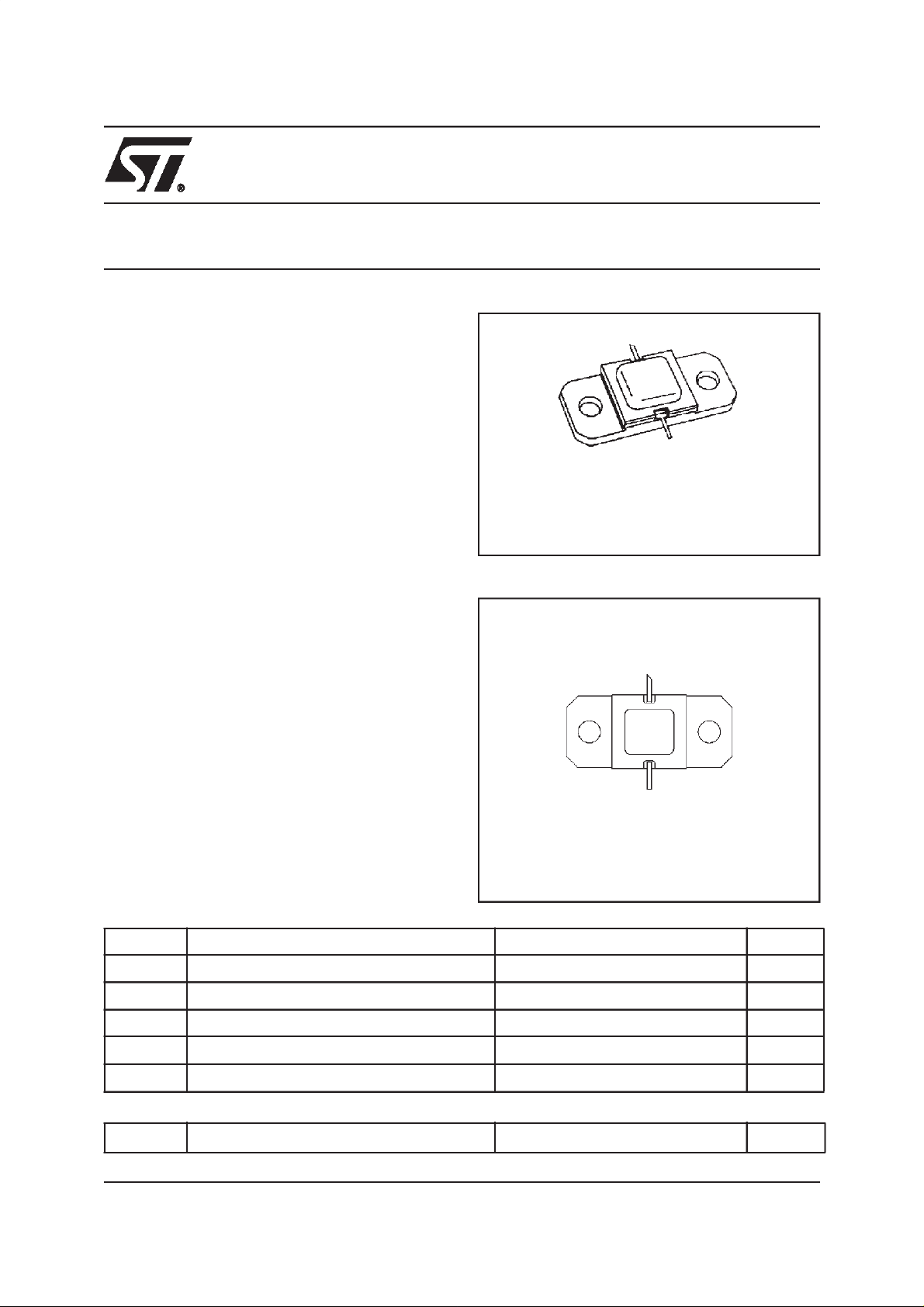
SO42
hermetically sealed
BRANDING
1517-25
PIN CONNECTION
DESCRIPTION
The AM1517-025 power transistor is designed
1
specifically for Satellite communications applications in the 1.5 - 1.7 frequency range.
The device is capable of withstanding any mismatch load condition at any phase angle (VSWR
∞:1) under full rated conditions. The unit is an
overlay, emitter site ballasted, geometry utilizing a
4
3
2
refractory/Gold metallization system.
The AM1517-025 is supplied in the AMPAC
TM
Hermetic/Ceramic package with internal Input/
Output matching structures.
ABSOLUTE MAXIMUM RATINGS(T
Symbol Parameter Value Unit
P
V
T
DISS
I
C
CC
T
STG
Power Dissipation* ( Tc≤ 500C)
Device Current* 2.5 A
Collector-Supply Voltage* 30 V
Junction Temperature 200 0
j
Storage Temperature -65 to +200 0
CASE
=250C)
1. Collector
2. Base
3. Emitter
4. Base
45 W
C
C
THERMAL DATA
R
th(j-c)
* Applies only to ratedRF amplifier operation
Junction-Case Thermal Resistance* 3.3
0
C/W
1/8May 2000
Page 2

AM1517-025
ELECTRICAL SPECIFICATION(T
CASE
=250C)
STATIC
Symbol Parameter Min. Typ. Max. Unit
BV
CBOIC
BV
EBOIE
I
CBO
h
FE
= 8 mA IE=0mA
= 8 mA IC=0mA
VCB=28V
VCE=5V IC= 1.6 A
45 --- --- V
3.0 --- --- V
--- --- 2 mA
15 --- 150 ---
REF. 1015989D
DYNAMIC
Symbol Parameter Min. Typ. Max. Unit
P
OUT
η
G
f = 1.5 - 1.7 GHz PIN=3.5W VCC=28V
f = 1.5 - 1.7 GHz PIN=3.5W VCC=28V
D
f = 1.5 - 1.7 GHz PIN=3.5W VCC= 28 V 8.5 --- --- dB
P
25 --- --- W
50 -- --- %
Note: AM1517 series vary P
to achieve P
IN
; performance guaranteed in 50 MHz increments.
OUT
Alpha-Suffix added toAM1517 P/N desigates band segment.
M - 1620 - 1660 MHz
S - 1625 - 1675 MHz
2/8
Page 3

TYPICAL PERFORMANCE
Output Power & Collector Efficiency vs Input Power Output Power vs Case Temperature
Collector Efficiency vs Case Temperature
AM1517-025
Output Power & Collector Efficiency vs Collector Voltage
Gain vs Case Temperature
3/8
Page 4

AM1517-025
IMPEDANCE DATA
TYPICAL INPUT
IMPEDANCE
Z
IN
=25W
P
OUT
V
=28V
CC
Z
= 50 OHMS
O
TYPICAL COLLECTOR
LOAD IMPEDANCE
Z
CL
=25W
P
OUT
V
=28V
CC
Z
= 50 OHMS
O
Frequency
MHz
Z
IN
(Ω)
Z
CL
(Ω)
1.5 GHz 8.5 + j 13.0 12.0 - j 4.0
1.6 GHz 8.0 + j 12.5 7.5 - j 4.5
1.7 GHz 9.0 + j 12.0 9.0 - j 6.0
4/8
Page 5

TEST CIRCUIT SCHEMATIC
AM1517-025
REV. 1022332D
TEST CIRCUIT COMPONENT PART LIST
C1,C2 0.4-2.5pF GIGA TRIM VARIABILE CAPACITOR
C3 100pF SURFACE MOUNT CERAMIC CHIP CAPACITOR
C4 1000pF RESIN SEALED # 8-35 THREADED FEEDTHRU CAPACITOR
C5
L1 3 TURN AIR WOUND COIL #26AWG, ID. 0.070 [1.77] BUS BAR WIRE
L2 3 TURN AIR WOUND COIL #26AWG, ID. 0.070 [1.77] BUS BAR WIRE
BOARD
µF/50v CERAMIC MOLDED RADIAL LEAD CAPACITOR
0.1
ALUMINA CERAMIC SUBSTRATE,HIGH POLISHED 1.0” SQ [25.40], 0.025” [0.63] THK.
200 MICROINCHES Au, BOTHSIDES
εr=9.6,
5/8
Page 6

AM1517-025
TEST CIRCUIT
TEST CIRCUIT PHOTOMASTER
0.773inches
1 inch
0.824 inches
6/8
Page 7

SO42 (.400 X .400 2/L HERM W/FLG) MECHANICAL DATA
AM1517-025
DIM.
A 0.51 0.76 .020 .030
B 6.35 .250
C 9.55 10.06 .376 .396
D 2.79 3.30 .110 .130
E 10.03 10.34 .395 .407
F 4.90 .193
G 11.43 .450
H 3.18 .125
I 16.26 16.76 .640 .660
J 22.61 23.11 .890 .910
K 10.03 10.54 .395 .415
L 0.10 0.18 .004 .006
M 1.32 1.83 .052 .072
N 2.84 3.35 .112 .132
P 5.84 .230
Q 22.35 23.37 .880 .920
MIN. TYP. MAX MIN. TYP. MAX
mm Inch
1011416B
7/8
Page 8

AM1517-025
Information furnished is believed to be accurate and reliable. However, STMicroelectronics assumes no responsibility for the consequences
of useof such informationnor for any infringement ofpatents orotherrightsofthird parties whichmayresult from its use.No license isgranted
by implication or otherwise under any patent or patent rights of STMicroelectronics. Specifications mentioned in this publication are subject
to change without notice. This publication supersedes and replaces all information previously supplied. STMicroelectronics products are not
authorized for use as critical components in life support devices or systems without express written approval of STMicroelectronics.
The ST logo is registered trademark of STMicroelectronics
2000 STMicroelectronics - All Rights Reserved
All other names are the property of their respective owners.
STMicroelectronics GROUP OF COMPANIES
Australia - Brazil - China - Finland - France - Germany - Hong Kong - India - Italy - Japan - Malaysia - Malta - Morocco -
Singapore - Spain - Sweden - Switzerland - United Kingdom - U.S.A.
http://www.st.com
,
8/8
 Loading...