

Page 1
RF & MICROWAVE TRANSISTORS
SATEL LITE COMMUNICATIO NS APPLI CATION S
.REFRACTORY/GOLD METALLIZATION
.EMITTER SITE BALLASTED
.
:1 VSWR CAPABILITY
∞
. LOW THERMAL RESISTANCE
.INPUT/OUTPUT MATCHING
.METAL/CERAMIC HERMETIC PACKAGE
.P
OUT
DESCRIPTION
The AM1517-012 power transistor isdesignedspecifically for Satellite communications applications
in the 1.5 − 1.7 GHz frequency range.
The device is capable of withstanding any mismatch load condition at any phase angle (VSWR
:1) under full rated conditions. The unit is an
∞
overlay, emitter site ballasted, geometry utilizing
a Refractory/Gold metallization system.
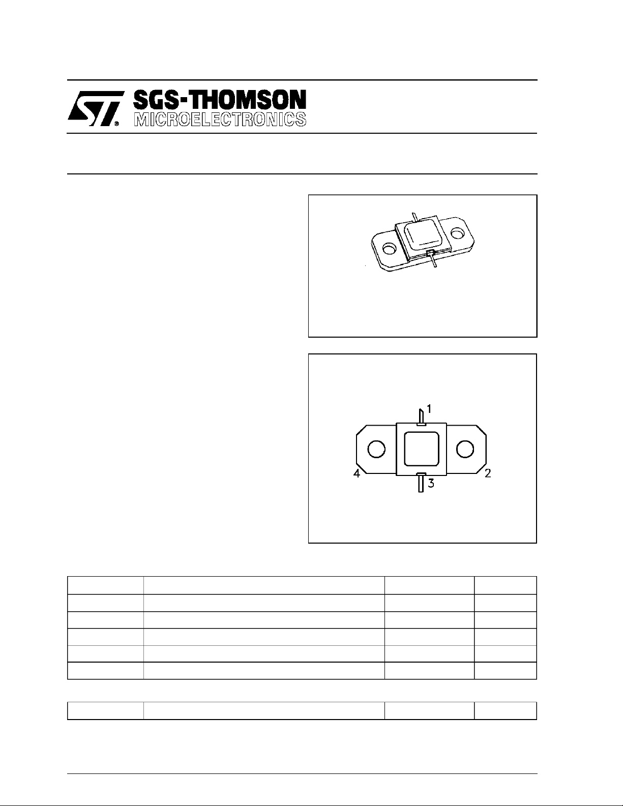
The AM1517-012 is supplied in the AMPAC Hermetic/Ceramic package with internal Input/Output
matching structures.
12 W MIN. WITH 8.5 dB GAIN
=
.400 x .400 2NLFL ( S042)
ORDER CODE
AM1517-012
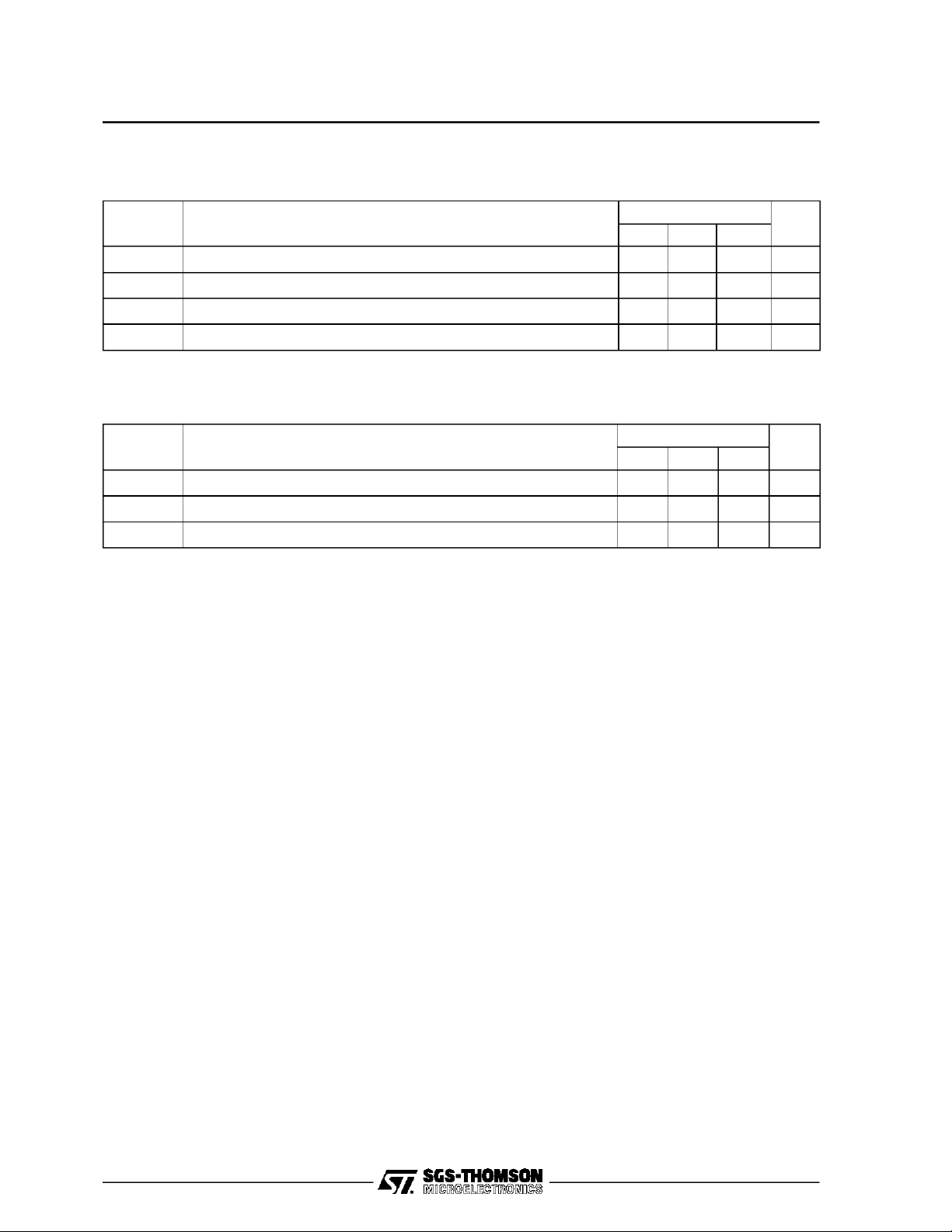
PIN CONNE C TIO N
1. Collector 3. Emitter
2. Base 4. Base
AM1517-012
hermeticallysealed
BRAN DING
1517-12
ABSOLUTE MAXIMUM RATINGS (T
Symbol Parameter Value Unit
P
DISS
I
C
V
CC
T
J
T
STG
THERMA L DAT A
R
TH(j-c)
*Appliesonly to rated RF amplifieroperation
September 1992
Power Dissipation* (TC≤100°C) 27 W
Device Current* 1.25 A
Collector-Supply Voltage* 30 V
Junction Temperature 200
Storage Temperature − 65 to +200
Junction-Case Thermal Resistance* 5.5 °C/W
case
= 25°C)
°
C
°
C
1/6
Page 2
AM1517-012
ELEC TRICA L SPEC IFI C A TIONS (Tcase = 25°C)
STATIC
Symbol Test Co ndition s
BV
CBO
BV
EBO
I
CBO
h
FE
DYNAMIC
Symb ol Test Conditi o ns
P
OUT
η
cf=1.5 — 1.7GHz P
G
P
Note: AM1517 series va r y PINto a chieve P
IC= 4mA IE= 0mA 45 — — V
IE= 4mA IC= 0mA 3.0 — — V
VCB= 28V — — 1 mA
VCE= 5V IC= .8A 15 — 150 —
f = 1.5 — 1.7GHz P
f = 1.5 — 1.7GHz P
Alpha-Suf fix added to AM1517 P/N designates band segment.
A -1500=1550 MHz
M - 1620=1660 MHz
S -1625=1675 MHz
1.7W V
IN =
1.7W V
IN =
1.7W V
IN =
; pe rformance guaranteed in 50 MHz i ncrements.
OUT
Value
Min. Typ. Max.
Value
Min. Typ. Max.
28V 12 13 — W
CC =
28V 55 58 — %
CC =
28V 8.5 — — dB
CC =
Unit
Uni t
2/6
Page 3

TYPICAL PERFORMAN CE
AM1517-012
TYPICAL PERFORMANCE vs
DRIVE POWER
COLLECTOR EFFICIENCY vs
POWER OUTPUT vs
TEMPERATURE
TEMPERATURE
TYPICAL PERFORMANCE vs
VOLTAGE @ FIXED DRIVE
GAIN vs TEMPERATURE
3/6
Page 4

AM1517-012
IMPEDA NCE DATA
TYPICAL INPUT
IMPEDANCE
Z
IN
P
= 12 W
OUT
VCC= 28 V
ZO= 50 ohms
FREQ. ZIN(Ω)Z
L = 1.50 GHz 13.0 + j 13.5 11.5 + j 5.0
M = 1.60 GHz 13.0 + j 12.0 10.5 + j 2.2
H = 1.70 GHz 14.5 + j 12.5 9.5−j 1.5
TYPICAL COLLECTOR
LOAD IMPEDANCE
Z
CL
P
= 12 W
OUT
VCC= 28 V
ZO= 50 ohms
CL
(Ω)
4/6
Page 5

TEST CIRCUIT
AM1517-012
All dimensions are in inches.
PACKAGE MECHANICAL DATA
5/6
Page 6

AM1517-012
Information furnished is believed to be accurate and reliable.However, SGS-THOMSON Microelectronics assumes no responsability for the
consequences of use of such information nor for any infringement of patents or other rights of third parties which may results from its use. No
license isgranted by implication or otherwiseunder any patent or patentrights of SGS-THOMSON Microelectronics. Specificationsmentioned
in this publicationare subject to change without notice. This publication supersedes and replaces all information previously supplied.
SGS-THOMSON Microelectronicsproductsare notauthorizedforuse ascritical componentsinlife supportdevices or systemswithout express
written approval of SGS-THOMSON Microelectonics.
1994 SGS-THOMSON Microelectronics- All Rights Reserved
Australia - Brazil - France - Germany - Hong Kong - Italy - Japan - Korea - Malaysia - Malta - Morocco - The Netherlands -
Singapore - Spain - Sweden - Switzerland - Taiwan - Thailand - UnitedKingdom - U.S.A
SGS-THOMSON MicroelectronicsGROUP OF COMPANIES
6/6
 Loading...