

Page 1
RF & MICROWAVE TRAN SIST ORS
L-BAND RADAR APPLICAT IONS
.REFRACTORY/GOLD METALLIZATION
.EMITTER SITE BALLASTED
.LOW THERMAL RESISTANCE
.INPUT/OUTPUT MATCHING
.OVERLAY GEOMETRY
.METAL/CERAMIC HERMETIC PACKAGE
.P
OUT
DESC RIPTION
The AM1214-200 device is a high power Class
C transistor specifically designedfor L-Band Radar
pulsed output and driver applications.
This device is capable of operation over a wide
range of pulse widths, duty cycles and temperatures, and wiil tolerate severe mismatch and overdrive conditions. Low RF thermal resistance and
computerized automatic wire bonding techniques
ensure high reliability and product consistency.
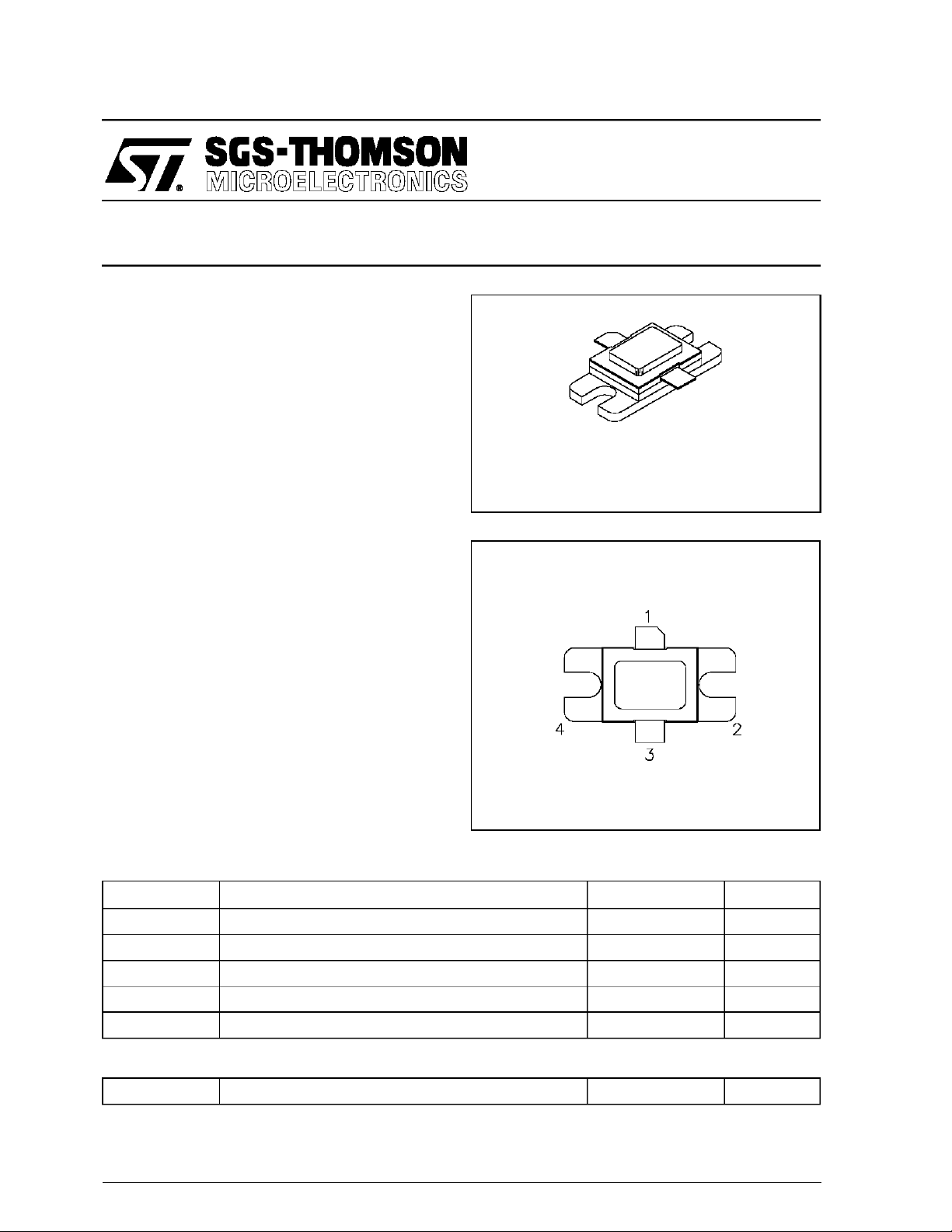
AM1214-200 is supplied in the BIGPAC hermetic
metal/ceramic package with internal input/output
matching structures.
200 W MIN. WITH 7.0 dB GAIN
=
.400 x .500 2LFL ( M205)
ORDER CODE
AM1214-200
PIN CO NNE C TIO N
1. Collector 3. Emitter
2. Base 4. Base
AM1214-200
PRELIMINARY DATA
hermetically sealed
BRANDING
1214-200
ABSOLUTE MAXIMUM RATINGS (T
Symbol Parameter Value Uni t
P
DISS
I
C
V
CC
T
J
T
STG
THERMA L DATA
R
TH(j-c)
*Appliesonly torated RF amplifieroperation
September 1992
Power Dissipation* (TC≤ 100°C) 575 W
Device Current* 16 A
Collector-Supply Voltage* 40 V
Junction Temperature (Pulsed RF Operation) 250
Storage Temperature − 65 to +200
Junction-Case Thermal Resistance* 0.26
case
= 25°C)
°
°
°
C/W
C
C
1/4
Page 2
AM1214-200
ELECTRICAL SPECIFICATIONS (T
case
= 25°C)
STATIC
Symbol Test Conditions
BV
BV
BV
I
CES
h
CBO
EBO
CES
FE
IC= 50mA IE= 0mA 70 — — V
IE= 30mA IC= 0mA 3.0 — — V
IC = 50mA VBE= 0V 70 — — V
VBE= 0V VCE= 40V — — 30 mA
VCE= 5V IC= 500mA 10 — — —
DYNAMIC
Symbol Test Conditi ons
P
OUT
η
cf=1215 — 1400MHz P
G
P
Note: Pulse Width
f = 1215 — 1400MHz P
f = 1215 — 1400MHz P
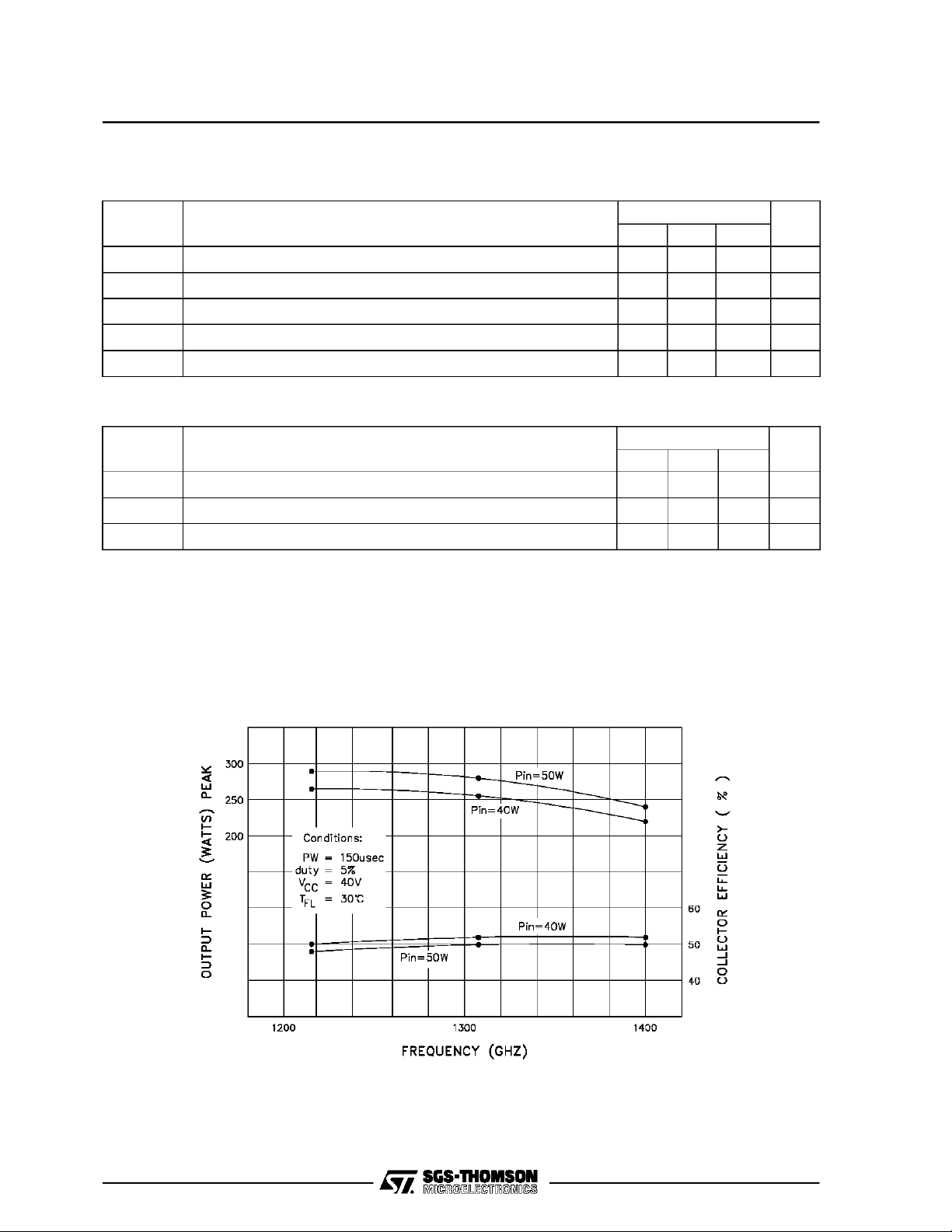
150µSec
=
Duty Cycle=5%
40W V
=
IN
40W V
=
IN
40W V
=
IN
Value
Min. T yp. Max.
Value
Min. Typ. Max.
40V 200 — — W
=
CC
40V 45 — — %
=
CC
40V 7.0 — — dB
=
CC
Unit
Unit
TYPICA L P ERFO R MA NCE
POWER OUTPUT & COLLECTOR
EFFICIENCY vs FREQUENCY
2/4
Page 3

IMPEDA NCE D ATA
TYPICAL I NPUT
IMPEDANCE
Z
IN
TYPICAL COLLECTOR
LOAD I MPEDANCE
AM1214-200
L
Z
IN
H
Z
CL
H
Z
CL
L
FREQ. ZIN(Ω)Z
CL
L=1215 MHz 2.7 + j 7.0 1.7 − j 4.0
M=1300 MHz 3.0 + j 4.8 1.4 − j 4.0
H=1400 MHz 1.8 + j 1.7 1.0 − j 2.0
TEST CIRCUIT
(Ω)
P
40W
=
IN
V
40V
=
CC
Normalized to 50 ohms
All dimensions are in millimeters.
Substrate 0.025” Thick AL203(Er=9.8)
C1,C2: 0.6 - 4.5 pF Johanson 7475 Variable Capacitor
C3 : 100 pF Case B Chip Capacitor
C4 : 100µF, 63V Electrolytic Capacitor
C5 : 68 pF Case B Chip Capacitor
C6 : 620 pF Case B Chip Capacitor
C7 : 0.1µF Ceramic Capacitor
C8 : Feedthrubypass 1200 pF
L1 : .018” OD Wire - Placement is Critical
L2 : 4 Turn .018” OD Inductor
3/4
Page 4

AM1214-200
PACKAGE MECHANICAL DATA
Information furnished is believed to be accurate and reliable.However, SGS-THOMSON Microelectronics assumes no responsability for the
consequences of use of such information nor for any infringementof patents orother rights of third parties which may results from its use. No
license isgranted by implicationor otherwise underany patent or patentrights of SGS-THOMSON Microelectronics.Specificationsmentioned
in this publication are subject to changewithout notice. Thispublication supersedes and replaces all information previously supplied.
SGS-THOMSON Microelectronicsproductsare notauthorizedforuse ascritical componentsin lifesupport devicesor systemswithout express
written approval of SGS-THOMSON Microelectonics.
1994 SGS-THOMSON Microelectronics - All RightsReserved
Australia - Brazil - France - Germany - Hong Kong - Italy - Japan - Korea - Malaysia - Malta - Morocco - The Netherlands -
Singapore - Spain - Sweden - Switzerland - Taiwan - Thailand - United Kingdom - U.S.A
SGS-THOMSON MicroelectronicsGROUP OF COMPANIES
4/4
 Loading...