

Page 1
RF & MICROWAVE TRANSISTORS
L-BAND RADAR APPLICA TIONS
.REFRACTORY/GOLD METALLIZATION
.EMITTER SITE BALLASTED
. 3: 1 VSWR CAPABILITY
. LOW THERMAL RESISTANCE
.INPUT/OUTPUT MATCHING
.O VERLAY GEOMETRY
.METAL/CERAMIC HERMETIC PACKAGE
.P
= 160 W MIN. WITH 7.3 dB GAIN
OUT
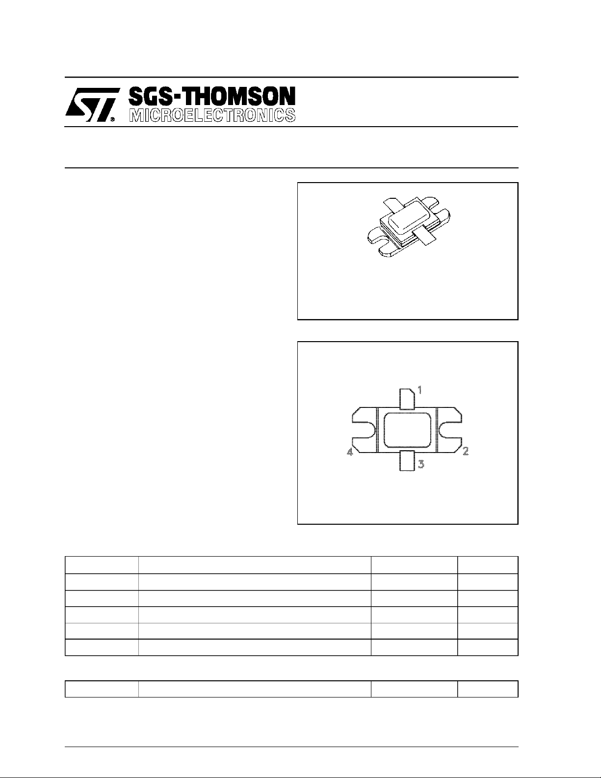
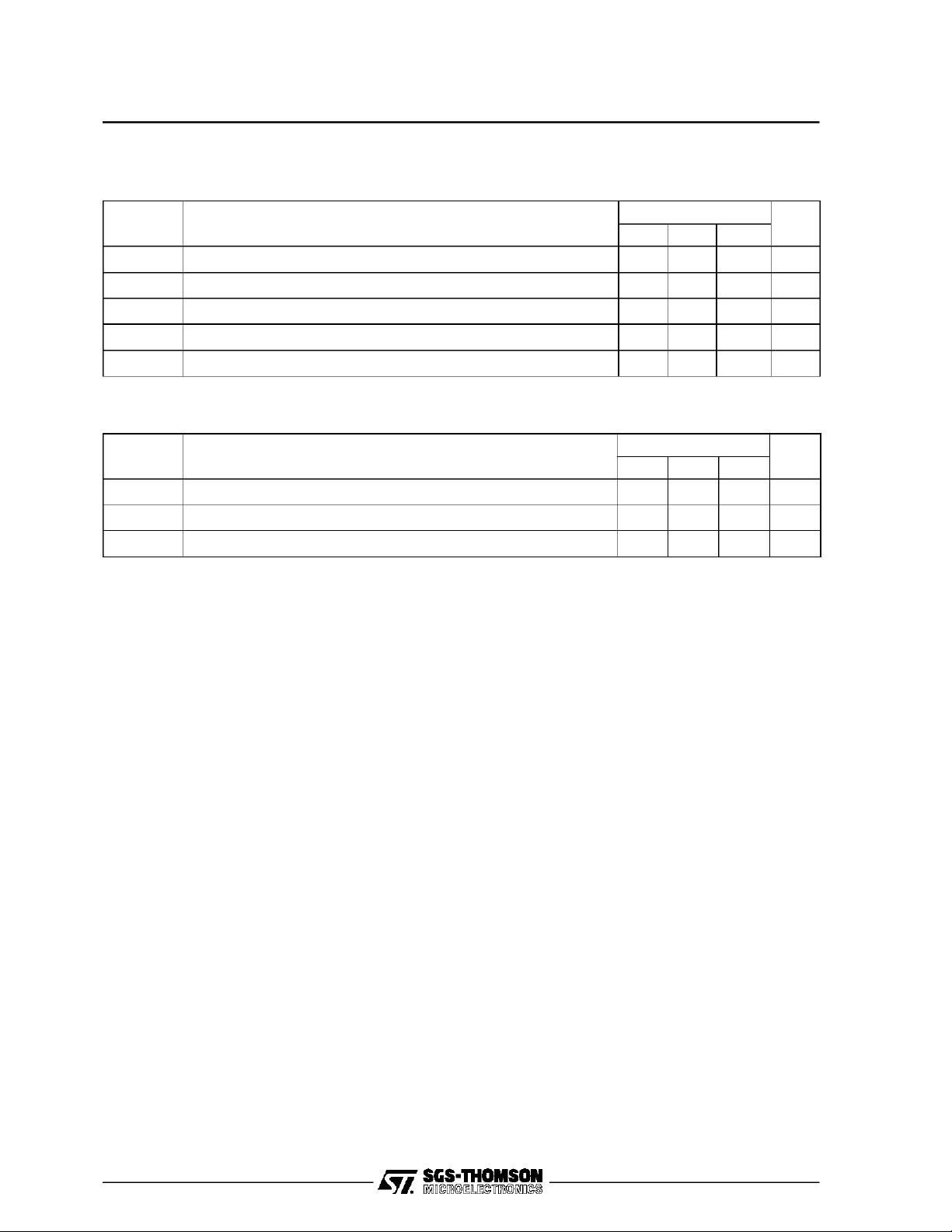
AM1214-175
.400 x . 500 2LFL (S038)
hermetically sealed
ORDER CODE
AM1214-175
DESC RIPT ION
The AM1214-175 device is a high power Class
C transistor specifically designed for L-Band radar
pulsed output and driver applications.
This device is capable of operation over a wide
range of pulse widths, duty cycles and temperatures and is capable of withstanding 3:1 output
VSWR at rated RF conditions. Low RF thermal
resistance and computerized automatic wire bonding techniques ensure high reliability and product
consistency.
The AM1214-175 is supplied in the BIGPAC Hermetic M etal/ Cerami c package wi th i nternal
Input/Output matching structures.
ABSOLU TE MAXIMUM RAT ING S (T
Symbol Parameter Value Uni t
P
T
DISS
I
V
CC
T
STG
C
J
Power Dissipation* (TC≤ 100°C) 330 W
Device Current* 14 A
Collector-Supply Voltage* 45 V
Junction Temperature (Pulsed RF Operation) 250
Storage Temperature − 65 to +200
case
= 25°C)
PIN CONNEC TIO N
1. Collector 3. Emitter
2. Base 4. Base
BRANDING
1214-175
°
C
°
C
THERMA L DATA
R
TH(j-c)
*Appliesonly torated RFamplifieroperation
September 1992
Junction-Case Thermal Resistance* 0.45 °C/W
1/6
Page 2
AM1214-175
ELEC TRICAL SPECI F ICA TI ONS (T
case
= 25°C)
STATIC
Symbol Test Condi tion s
BV
BV
BV
I
CES
h
CBO
EBO
CES
FE
IC= 60mA IE= 0mA 65 — — V
IE= 10mA IC= 0mA 3.5 — — V
IC = 100mA 65 — — V
VCE= 40V — — 25 mA
VCE= 5V IC= 5A 15 — 150 —
DYNAMIC
Symb ol Test Condi tions
P
OUT
η
cf=1215 — 1400MHz P
G
P
Note: Pulse Widt h
f = 1215 — 1400MHz P
f = 1215 — 1400MHz P
150µS
=
Duty Cycl e=5%
30W V
=
IN
30W V
=
IN
30W V
=
IN
Value
Min. Typ. Max.
Value
Min. Typ. Max.
40V 160 180 — W
=
CC
40V 45 50 — %
=
CC
40V 7.3 7.8 — dB
=
CC
Unit
Unit
2/6
Page 3

TYPICAL PERFO RM AN CE
TYPICAL BROADBAND
POWER A M PLIFIER
AM1214-175
RELATIVE POWER OUTPUT AND
COLLECTOR EFFICIENCY vs
COLLECTOR VOLTAGE
MAXIMUM THERMAL RESISTANCE vs PULSE WIDTH & DUTY CYCLE
3/6
Page 4

AM1214-175
IMPEDA NCE D ATA
TYPICAL INPUT
IMPEDANCE
Z
IN
PIN= 30 W
VCC= 40 V
Z0*=50 ohms
FREQ. ZIN(Ω)Z
L = 1215 MHz 4.0 + j 3.5 2.0 − j 2.5
M = 1300 MHz 2.0 + j 3.0 2.0 − j 1.5
H = 1400 MHz 1.5 + j 4.0 1.5 − j 2.5
TYPICAL COLLECTOR
LOAD IMPEDANCE
Z
CL
PIN= 30 W
VCC= 40 V
Z0* = 50 ohms
CL
(Ω)
4/6
*Normalized Impedance
Page 5

TEST CIRCUIT
AM1214-175
Ref. Dwg. No.: 104-001280
PACKAGE MECHANICAL DATA
5/6
Page 6

AM1214-175
Information furnishedis believed to be accurate and reliable.However, SGS-THOMSON Microelectronicsassumes no responsability for the
consequences of use of such information norfor any infringement of patents or other rights of third parties which mayresults from its use. No
license is granted by implication or otherwise underany patent or patent rights of SGS-THOMSON Microelectronics. Specificationsmentioned
in this publication are subject to change without notice. This publication supersedes and replaces all information previously supplied.
SGS-THOMSON Microelectronicsproductsare notauthorized foruse ascritical componentsinlifesupportdevices or systemswithoutexpress
written approval of SGS-THOMSON Microelectonics.
1994 SGS-THOMSON Microelectronics - All Rights Reserved
Australia - Brazil - France- Germany - Hong Kong - Italy - Japan - Korea - Malaysia - Malta - Morocco - The Netherlands-
Singapore - Spain - Sweden- Switzerland - Taiwan - Thailand - United Kingdom - U.S.A
SGS-THOMSON Microelectronics GROUP OF COMPANIES
6/6
 Loading...