

Page 1
RF & MICROWAVE TRANSISTORS
.REFRACTORY/GOLD METALLIZATION
.EMITTER SITE BALLASTING
.LOW RF THERMAL RESISTANCE
.INPUT/OUTPUT MATCHING
.OVERLAY GEOMETRY
.METAL/CERAMIC HERMETIC PACKAGE
.P
OUT =
325 W MIN. WITH 7.7 dB GAIN
.1030/1090 MHZ OPERATION
AM1011-300
AVIONI CS APPLICAT IONS
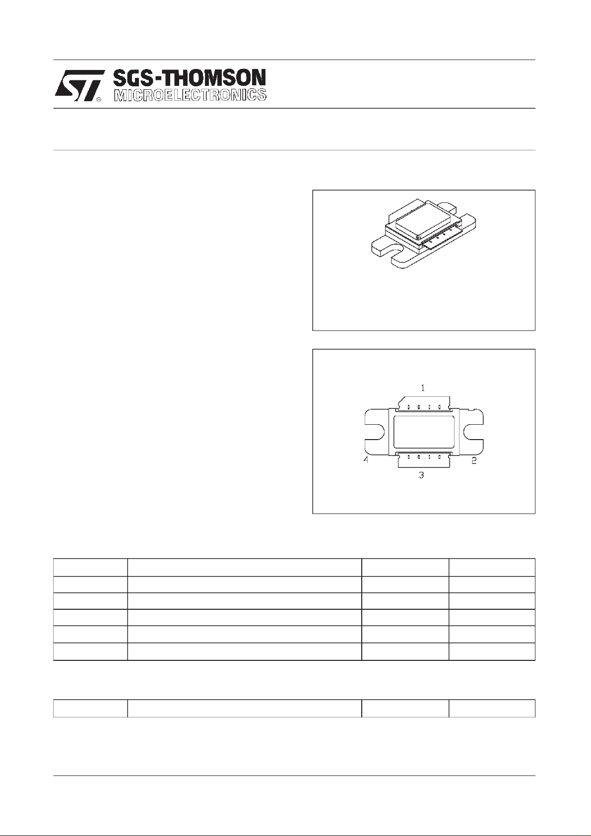
.400x.6002LFL(M207)
hermeticallysealed
ORDER C OD E
AM1011-300
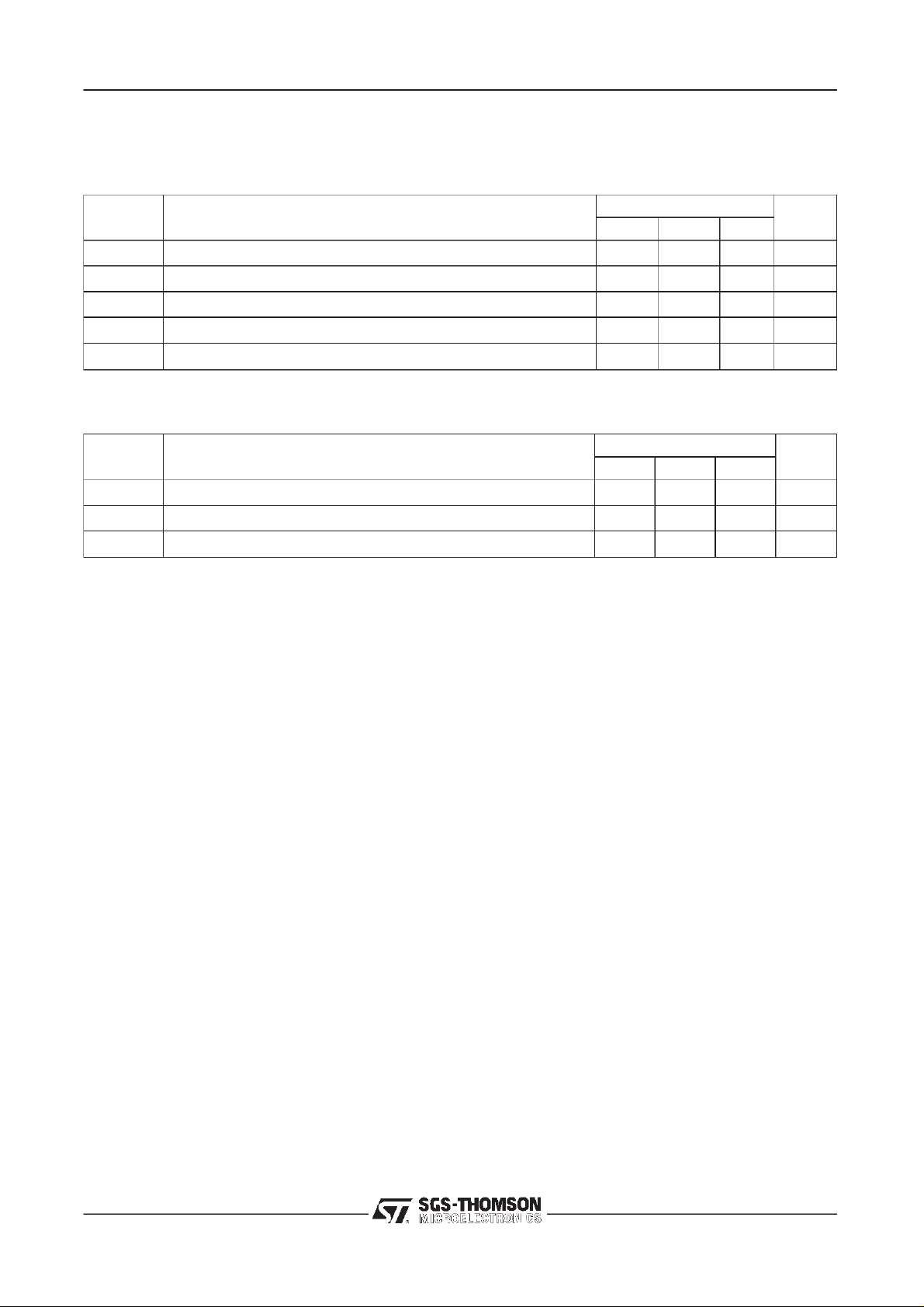
PI N CONNECTION
DESCRIP TION
The AM1011-300 is a rugged, Class C common
base device specifically designed for new ModeS interrogator and transponder applications.
Minimal amplitude droop over the heavy Mode-S
pulse burst is guaranteedby a thermal design incorporating an overlay site-ballasted die geometry.
ABSOLUTE MAXIMUM RATINGS (T
Symbol Parameter Value Unit
P
V
T
DISS
I
C
CC
T
J
STG
Power Dissipation (TC≤100°C)*
Device Current* 36 A
Collector-SupplyVoltage* 43 V
Junction Temperature(Pulsed RF operation) +250
Storage Temperature
case
= 25°C)
1. Collector 3. Emitter
2. Base 4. Base
1070 W
65 to +200
−
BRAND I NG
AM1011-300
°
C
°
C
THERMAL DAT A
R
TH(j-c)
*Applies onlytoratedRF amplifieroperation.
December 9, 1997 1/5
Junction-CaseThermal Resistance* 0.14
°C/W
Page 2
AM1011-300
ELECTRICAL SPECIFICATIONS (T
case
= 25°C)
STATIC
Symbol Test Conditions
BV
BV
BV
I
CES
h
CBO
CES
EBO
FE
IC= 75 mA IE= 0mA
IC= 75 mA VBE= 0V
IC= 25 mA IC= 0mA
VCE= 40 V VBE= 0V
VCE= 5V IC=10 A
DYNAMIC
Symbol Test Condi tions
P
OUT f = 1090 MHz P
hc
G
Pulse Conditi ons: Pulse w idth = 200µs , Duty C ycle = 5%, are equi valent t o the foll owing
f = 1090 MHz P
P f = 1090 MHz P
puls e burst c ondit i ons:
Mode- S Int er rogato r (f r eq = 1030MH z)
32 pulses, 32µs on, 18µs off, burst perio d = 17.6ms
long term duty = 5.82%
= 55 W VCC= 40 V
IN
= 325 W VCC= 40 V
OUT
= 325 W VCC= 40 V
OUT
Value
Min. Typ. Max.
Uni t
65 — — V
65 — — V
3.0 — — V
— — 30 mA
10———
Value
Min. Typ. Max.
Uni t
325 350 — W
40 45 — %
7.7 8.0 — dB
2/5 December 9, 1997
Page 3

TYPI CAL PE RFO RMANCE
AM 1011-300
POWER OUTPUT vs POWER INPUT
@ 1030 MHz
MAXIMUM THERMAL RESISTANCE vs
POWER OUTPUT vs POWER INPUT
@1090MHz
PULSE WIDTH
TC=40°C
P
= 50W
IN
V
= 40V
CC
Duty Cycle = 5%
December 9, 1997 3/5
Page 4

AM1011-300
IMPEDANCE DATA
TYPICAL INPUT
IMPEDANCE
Z
IN
COLLECTOR LOAD
TEST CIRCUIT
TYPICAL
Z
CL
FREQ.
Z
1030 MHz 0.7 + j 4.1
1090 MHz 0.65 + j 4.2
= 55W
P
IN
(Ω)Z
IN
CL
(Ω)
0.78 − j 2.4
0.4 − j 2.4
4/5 December 9, 1997
Page 5

PACKAGE MECHANICAL DATA
Ref.: Dwg. No. 12-0207
UDCS No. 1011408rev B
AM 1011-300
Information furnished is believed to be accurate and reliable. However, SGS-THOMSON Microelectronics assumes no responsibility for the
consequences of use of such information nor for any infringement of patents or other rights of third parties which may result from its use.
No license is granted by implication or otherwise under any patent or patent rights of SGS-THOMSON Microelectronics. Specifications
mentioned in this publication are subject to change without notice. This publication supersedes and replaces all information previously
supplied. SGS-THOMSON Microelectronics products are not authorized for use as critical components in life support devices or systems
without express written approval of SGS-THOMSON Microelectronics.
1997 SGS-THOMSON Microelectronics - All Rights Reserved
Australia - Brazil - Canada - China - France - Germany - Italy - Japan - Korea
Malaysia - Malta - Morocco - The Netherlands - Singapore - Spain - Sweden - Switzerland
SGS-THOMSON Microelectronics GROUP OF COMPANIES
Taiwan - Thailand - United Kingdom - U.S.A.
December 9, 1997 5/5
 Loading...