

Page 1
RF & MICROWAVE TRANSISTORS
L-BAND AVI ONICS APPL ICATIO NS
.REFRACTORY/GOLD METALLIZATION
.EMITTER SITE BALLASTED
. 10: 1 VSWR CAPABILITY
. LOW THERMAL RESISTANCE
.INPUT/OUTPUT MATCHING
.O VERLAY GEOMETRY
.METAL/CERAMIC HERMETIC PACKAGE
.P
= 75 W MIN. WITH 9.2 dB GAIN
OUT
.400 x .400 2LFL (S036)
ORDER CODE
AM1011-075
AM1011-075
hermeticallysealed
BRAN DI NG
1011-75
DESCRIPTION
The AM1011-075 device is a high power Class
C trans istor s pecifi ca lly designed for L- Band
Avionics transponder/interrogator pulsed output
and driver applications.
This device is capable of operation over a wide
range of pulse widths, duty cycles, and temperatures and is capable of withstanding 10:1 output
VSWR at rated RF conditions. Low RF thermal
resistance and computerized automatic wire bonding techniques ensure high reliability and product
consistency.
The AM1011-075 is supplied in the AMPAC Her-
metic Met al/C eramic package wit h internal
Input/Output matching structures.
ABSOLU TE M AXI MUM RAT ING S (T
Symbol Parameter Value Unit
P
T
DISS
I
V
CC
T
STG
C
J
Power Dissipation* (TC≤ 100°C) 175 W
Device Current* 5.4 A
Collector-Supply Voltage* 55 V
Junction Temperature (Pulsed RF Operation) 250
Storage Temperature − 65 to +200
case
25°C)
=
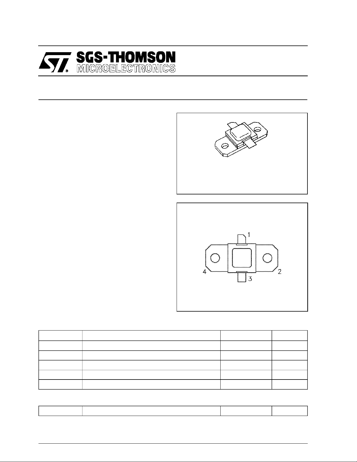
PIN CO NNE C TIO N
1. Collector 3. Emitter
2. Base 4. Base
°
C
°
C
THERMA L DATA
R
TH(j-c)
*Appliesonly to rated RF amplifieroperation
September 1992
Junction-Case Thermal Resistance* 0.86 °C/W
1/4
Page 2
AM1011-075
ELEC TRICA L SPECI F ICATIONS (T
case
=
STATIC
Symbol Test Co ndition s
BV
BV
BV
I
CES
h
CBO
EBO
CER
FE
I
10mA I
=
C
I
4mA I
=
E
0mA 65 — — V
=
E
0mA 3.5 — — V
=
C
IC = 20mA RBE= 10Ω 65 — — V
V
50V — — 6 mA
=
CE
V
5V I
=
CE
1mA 10 — — —
=
C
DYNAMIC
Symb ol Test Co n dition s
P
OUT
η
cf=1090MHz P
G
P
Note: Pulse Width
f=1090MHz P
f=1090MHz P
32µSec
=
Duty Cycl e=2%
9W Peak V
=
IN
9W Peak V
=
IN
9W Peak V
=
IN
25°C)
Value
Min. Typ. Max.
Value
Min. Typ. Max.
50V 75 84 — W
=
CC
50V 48 56 — %
=
CC
50V 9.2 9.7 — dB
=
CC
Unit
Uni t
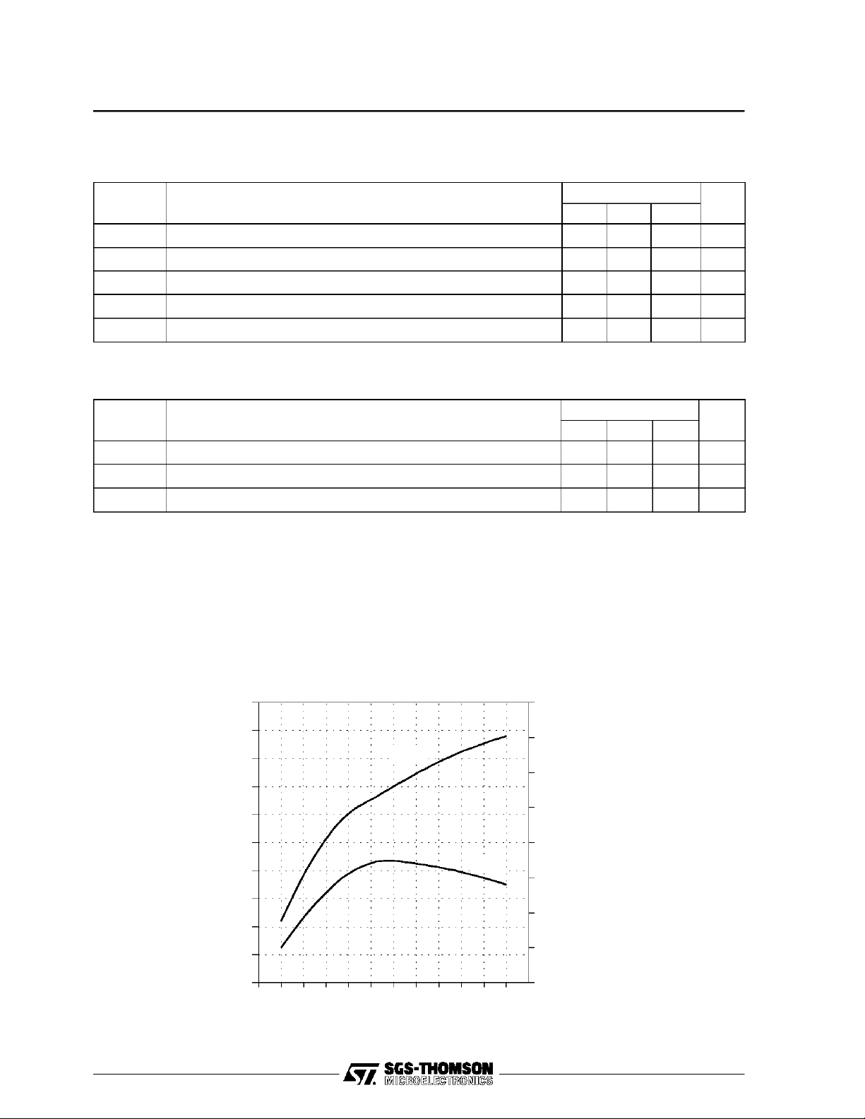
TYPICAL PERFO RM AN CE
120
110
P
O
100
W
E
90
R
O
80
U
T
70
P
U
60
T
50
W
A
40
T
T
S
30
20
45678910111213141516
TYPICAL POWER OUTPUT & COLLECTOR
TYPICAL POWER OUTPUT &
EFFICIENCY vs POWER INPUT
COLLECTOR EFFICIENCY vs
POWER INPUT
P
OUT
η
C
POWER INPUT (WATTS)
POWER INPUT (WATTS)
80
75
C
O
70
L
L
E
65
C
T
O
60
R
E
55
F
F
50
.
%
45
40
2/4
Page 3

IMPEDA NCE D ATA
TYPICAL I N PUT
IMPEDANCE
Z
IN
AM1011-075
TYPICAL COL LECTOR
LOAD IMPEDANCE
Z
CL
FREQ. ZIN(Ω)Z
CL
L=1030 MHz 7.0 + j 3.0 12.5 − j 4.5
H=1090 MHz 11.0 + j 1.5 13.0 − j 3.0
TEST CIRCUIT
(Ω)
IN
L
Z
H
H
Z
CL
L
PIN= 9.0 W
V
50 V
=
CC
Normalized to 50 ohms
All dimensions are in inches.
Substrate material: .025 thick AI2O
C1 : 0.8—8.0 pF Johanson Gigatrim Capacitor
C2 : 100 pF Chip Capacitor
C3 : 1500 pF Filtercon Feedthru
3
C4 : 1 µF, Ceramic Capacitor
C5 : 100 µF, Electrolytic Capacitor
RFC 1: Au Plated Ni Strap
RFC 2: #26 Wire, 4 Turn 1/16 I.D.
0.280 Long x 0.035 Wide x 0.005 Thick
3/4
Page 4

AM1011-075
PACKAGE MECHANICAL DATA
Information furnished is believed to be accurate and reliable.However, SGS-THOMSON Microelectronics assumes no responsability for the
consequences of use of such information nor for any infringement of patents or other rights of third parties which may results from its use. No
license isgranted by implication or otherwiseunder any patent or patentrights of SGS-THOMSON Microelectronics. Specificationsmentioned
in this publication are subject to change without notice. This publication supersedes and replaces all information previously supplied.
SGS-THOMSON Microelectronicsproductsare notauthorizedfor use ascritical componentsinlife supportdevices or systemswithout express
written approval of SGS-THOMSON Microelectonics.
1994 SGS-THOMSON Microelectronics- All Rights Reserved
Australia - Brazil - France - Germany - Hong Kong - Italy - Japan - Korea - Malaysia - Malta - Morocco - The Netherlands -
Singapore - Spain - Sweden - Switzerland - Taiwan - Thailand - United Kingdom - U.S.A
SGS-THOMSON MicroelectronicsGROUP OF COMPANIES
4/4
 Loading...