

Page 1
RF & MICROWAVE T RANSISTORS
L-BAND AVION ICS A PPLICA TIONS
.REFRACTORY/GOLD METALLIZATION
.EMITTER SITE BALLASTED
.LOW THERMAL RESISTANCE
.INPUT/OUTPUT MATCHING
.OVERLAY GEOMETRY
.METAL/CERAMIC HERMETIC PACKAGE
.P
= 70 W MIN. WITH 6.7 dB GAIN
OUT
AM1011-070
.400 x .400 2NL F L (S 042)
hermetically sealed
ORDER CODE
AM1011-70
DESCRIPTION
The AM1011-070 device is a high power Class
C t rans ist or spec ifically designed for L-Band
Avionics transponder/interrogator pulsed output
and driver applications.
This device is capable of operation over a wide
range of pulse widths, duty cycles and temperatures and is capable of withstanding severe output
VSWR at rated RF conditions. Low RF thermal
resistance and computerized automatic wire bonding techniques ensure high reliability and product
consistency.
The AM1011-070 is supplied in the AMPAC Her-
metic Met al/C eramic package with i nternal
Input/Output matching structures.
ABSOLU TE M AXI MUM RATING S (T
Symbol Parameter Value Uni t
P
T
DISS
I
V
CC
T
STG
C
J
Power Dissipation* (TC≤ 100°C) 200 W
Device Current* 8.0 A
Collector-Supply Voltage* 32 V
Junction Temperature (PulsedRF Operation) 250
Storage Temperature − 65 to +200
case
= 25°C)
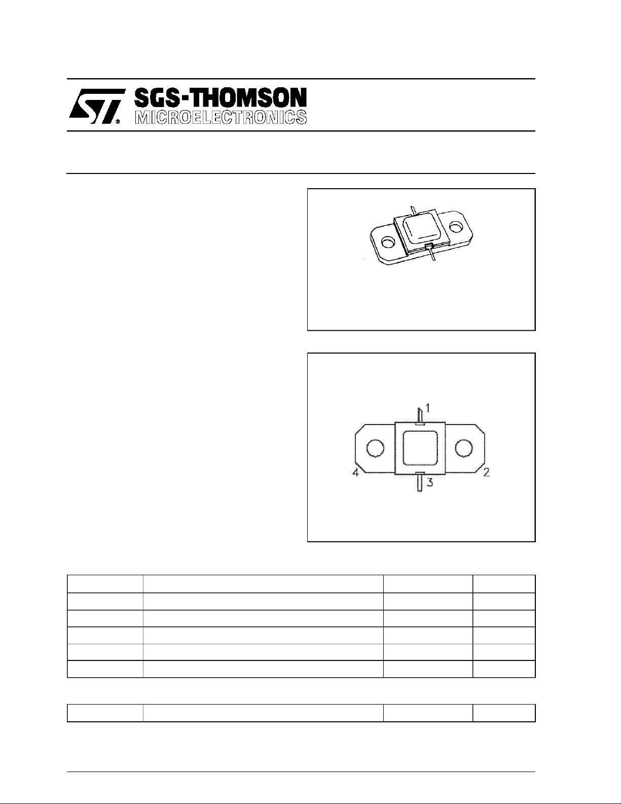
PIN CON NE CTI ON
1. Collector 3. Emitter
2. Base 4. Base
BRAND I NG
1011-70
°
C
°
C
THERMA L DATA
R
TH(j-c)
*Appliesonly to rated RFamplifieroperation
September 1992
Junction-Case Thermal Resistance* 0.68 °C/W
1/4
Page 2
AM1011-070
ELEC TRIC AL SPEC IFICATI ON S (T
case
= 25°C)
STATIC
Symbol Test Conditions
BV
BV
BV
I
CES
h
CBO
EBO
CER
FE
IC= 25mA IE= 0mA 55 — — V
IE= 10mA IC= 0mA 3.5 — — V
IC = 25mA RBE= 10Ω 55 — — V
VCE= 35V — — 20 mA
VCE= 5V IC= 2mA 20 — 200 —
Min. Typ. Max.
Value
DYNAMIC
Symbol Test Cond itions
P
OUT
η
cf= 1090 MHz PIN= 15W VCC= 28V 45 — — %
G
P
Note: Pulse Width = 100µSec
f = 1090 MHz PIN= 15W VCC= 28V 70 — — W
f = 1090 MHz PIN= 15W VCC= 28V 6.7 — — dB
Duty Cycle = 2%
Value
Min. Typ. Max.
Unit
Unit
2/4
Page 3

IMPEDA NCE DATA
TYPICAL INPUT
IMPEDANCE
Z
IN
AM1011-070
TYPICAL COLLECTOR
LOAD I MPEDANCE
PIN= 15 W
VCC= 28 V
Normalized to 50 ohms
TEST CIRCUIT
Ref. Dwg. No. J313119
FREQ. ZIN(Ω)Z
CL
(Ω)
L = 1025 MHz 4.7 + j 4.7 3.6 + j 4.3
H = 1090 MHz 4.7 + j 3.9 3.3 + j 4.4
Z
CL
All dimensions are in inches.
Substrate material: .025 thick AI2O
C1 : 0.3—3.5 pF JohansonGigatrim Capacitor
C2 : 0.3—3.5 pF JohansonGigatrim Capacitor
C3 : 100 pF Chip Capacitor
C4 : 1500 pF Erie Feedthru, or Equiv.
3
C5 : 100 MF Electrolytic Capacitor, 50V
C6 : 1500 pF Erie Feedthrough, or Equiv.
L1 : #32 Wire, 4 Turn .062 I.D.
L2 : #32 Wire, 4 Turn .062 I.D.
RBE : 0 — 1.0 Ohm
3/4
Page 4

AM1011-070
PACKAGE MECHANICAL DATA
Information furnished is believed to be accurate and reliable. However, SGS-THOMSON Microelectronics assumes no responsability for the
consequences of use of such information nor for any infringement of patents or other rights of third parties which may results from its use. No
license isgrantedby implication or otherwiseunder any patent or patentrights ofSGS-THOMSON Microelectronics. Specificationsmentioned
in this publication are subject to change without notice. This publication supersedes and replaces all information previously supplied.
SGS-THOMSON Microelectronicsproductsare notauthorizedforuseascritical componentsinlife supportdevices or systemswithout express
written approval of SGS-THOMSON Microelectonics.
1994 SGS-THOMSON Microelectronics- All RightsReserved
Australia - Brazil - France - Germany - Hong Kong - Italy - Japan - Korea - Malaysia - Malta - Morocco - The Netherlands -
Singapore - Spain - Sweden- Switzerland - Taiwan - Thailand - UnitedKingdom - U.S.A
SGS-THOMSON MicroelectronicsGROUPOFCOMPANIES
4/4
 Loading...