

Page 1
RF & MICROWAVE TRAN SIST ORS
.REFRACTORY/GOLD METALLIZATION
.EMITTER SITE BALLASTED
. LOW THERMAL RESISTANCE
.INPUT/OUTPUT MATCHING
.O VERLAY GEOMETRY
.METAL/CERAMIC HERMETIC PACKAGE
.P
= 150 W MIN. WITH 7.5 dB GAIN
OUT
.BANDWIDT H = 255MHz
AM0912-150
AVIONI CS APPLICAT IONS
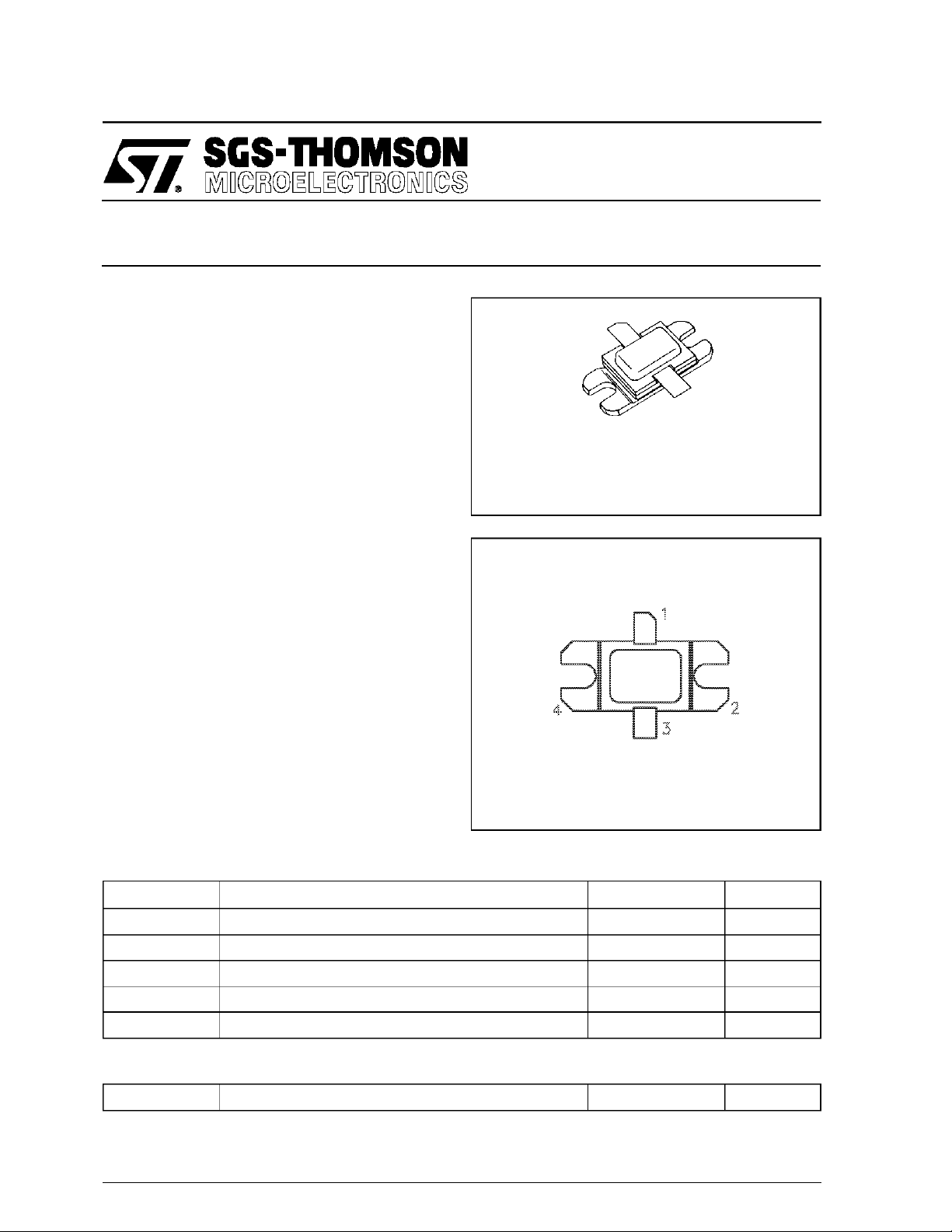
.400 x . 500 2LFL (S038)
hermetically sealed
ORDER CODE
AM0912-150
PIN CONNEC TIO N
BRANDING
0912-150
DESC RIPT ION
The AM0912-150 is des i gned for speciali z ed
avionics applications including Mode-S, TCAS and
JTIDS, where power is provided under pulse formats utilizing short pulse widths and high burst
or overall duty cycles.
The AM0912-150 is housed in the unique BIGPAC Hermetic Metal/Ceramic package with internal Input/Output matching structures.
ABSOLU TE MAXIMUM RAT ING S (T
Symbol Parameter Value Uni t
P
DISS
I
C
V
CC
T
J
T
STG
THERMA L DATA
R
TH(j-c)
Power Dissipation* (TC≤ 100°C) 300 W
Device Current* 16.5 A
Collector-Supply Voltage* 35 V
Junction Temperature (Pulsed RF Operation) 250
Storage Temperature − 65 to +200
Junction-Case Thermal Resistance* 0.57 °C/W
case
= 25°C)
1. Collector 3. Emitter
2. Base 4. Base
°
C
°
C
*Appliesonly to rated RFamplifieroperation
September 1992
1/6
Page 2
AM0912-150
ELEC TRICAL SPECI F ICA TI ONS (T
case
= 25°C)
STATIC
Symbol Test Condi tion s
BV
BV
BV
I
CES
h
CBO
EBO
CES
FE
IC= 60mA IE= 0mA 55 65 — V
IE= 10mA IC= 0mA 3.5 — — V
IC = 100mA 55 — — V
VCE= 35V — — 25 mA
VCE= 5V IC= 5A 20 — — —
DYNAMIC
Symb ol Test Condi tions
P
OUT
η
cf=960 — 1215MHz P
G
P
Note: Pulse Format: 6.4 µSon6.6µS off; repea t for 3.3 ms, then off for 4. 5125 ms
f = 960 — 1215MHz P
f = 960 — 1215MHz P
Duty Cycle: Burst 49.2% overall 20.8%
26.7W V
=
IN
26.7W V
=
IN
26.7W V
=
IN
35V 150 — — W
=
CC
35V 45 — — %
=
CC
35V 7.5 — — dB
=
CC
Value
Min. Typ. M ax.
Value
Min. Typ. Max.
Unit
Uni t
2/6
Page 3

TYPICAL PERFO RM AN CE
TYPICAL POWER INPUT, POWER
OUTPUT & COLLECTOR EFFICIENCY
vs FREQUENCY
AM0912-150
POWER OUTPUT & COLLECTOR
EFFICIENCY vs POWER INPUT
MAXIMU M THERMA L RESISTAN CE vs P U LSE WIDTH & D UT Y CYCLE
VCC= 28-35V
PIN≅ 26W
TC<45°C
3/6
Page 4

AM0912-150
IMPEDA NCE D ATA
TYPICAL INPUT
IMPEDANCE
Z
IN
PIN= 26.7 W
VCC= 35 V
ZO* = 10 ohms
FREQ. ZIN(Ω)Z
L = 960 MHz 2.1 + j 3.8 3.8 − j 3.6
• = 1000 MHz 1.5 + j 3.1 3.0 − j 2.4
M = 1050 MHz 1.2 + j 2.5 2.5 − j 2.0
• = 1150 MHz 1.5 + j 2.4 2.0 − j 2.0
H = 1215 MHz 1.7 + j 2.4 2.0 − j 2.5
TYPICAL COLLECTOR
LOAD IMPEDANCE
Z
CL
PIN= 26.7 W
VCC= 35 V
ZO* = 10 ohms
CL
(Ω)
*Normalized Impedance
4/6
Page 5

TEST CIRCUIT
Ref: Dwg. No. C127513
AM0912-150
5/6
Page 6

AM0912-150
PACKAGE MECHANICAL DATA
Information furnished is believed to be accurate and reliable. However, SGS-THOMSON Microelectronics assumes no responsability for the
consequences of use of such information nor for any infringement of patents or other rights of third parties which may results from its use. No
license isgrantedby implication or otherwiseunder any patent orpatentrights of SGS-THOMSON Microelectronics. Specificationsmentioned
in this publication are subject to change without notice. This publication supersedes and replaces all information previously supplied.
SGS-THOMSON Microelectronicsproductsare notauthorizedforuse ascritical componentsinlife supportdevices or systemswithout express
written approval of SGS-THOMSON Microelectonics.
1994 SGS-THOMSON Microelectronics- All Rights Reserved
Australia - Brazil - France - Germany - Hong Kong - Italy - Japan - Korea - Malaysia - Malta - Morocco - The Netherlands -
Singapore - Spain - Sweden- Switzerland - Taiwan - Thailand - UnitedKingdom - U.S.A
SGS-THOMSON MicroelectronicsGROUPOF COMPANIES
6/6
 Loading...